CN201252187Y - Card edge connector - Google Patents
Card edge connectorDownload PDFInfo
- Publication number
- CN201252187Y CN201252187YCNU2008200415724UCN200820041572UCN201252187YCN 201252187 YCN201252187 YCN 201252187YCN U2008200415724 UCNU2008200415724 UCN U2008200415724UCN 200820041572 UCN200820041572 UCN 200820041572UCN 201252187 YCN201252187 YCN 201252187Y
- Authority
- CN
- China
- Prior art keywords
- groove
- insulating body
- terminal
- bayonet connector
- connecting portion
- Prior art date
- Legal status (The legal status is an assumption and is not a legal conclusion. Google has not performed a legal analysis and makes no representation as to the accuracy of the status listed.)
- Expired - Lifetime
Links
Images


Classifications
- H—ELECTRICITY
- H01—ELECTRIC ELEMENTS
- H01R—ELECTRICALLY-CONDUCTIVE CONNECTIONS; STRUCTURAL ASSOCIATIONS OF A PLURALITY OF MUTUALLY-INSULATED ELECTRICAL CONNECTING ELEMENTS; COUPLING DEVICES; CURRENT COLLECTORS
- H01R12/00—Structural associations of a plurality of mutually-insulated electrical connecting elements, specially adapted for printed circuits, e.g. printed circuit boards [PCB], flat or ribbon cables, or like generally planar structures, e.g. terminal strips, terminal blocks; Coupling devices specially adapted for printed circuits, flat or ribbon cables, or like generally planar structures; Terminals specially adapted for contact with, or insertion into, printed circuits, flat or ribbon cables, or like generally planar structures
- H01R12/70—Coupling devices
- H01R12/71—Coupling devices for rigid printing circuits or like structures
- H01R12/72—Coupling devices for rigid printing circuits or like structures coupling with the edge of the rigid printed circuits or like structures
- H01R12/721—Coupling devices for rigid printing circuits or like structures coupling with the edge of the rigid printed circuits or like structures cooperating directly with the edge of the rigid printed circuits
Landscapes
- Coupling Device And Connection With Printed Circuit (AREA)
- Details Of Connecting Devices For Male And Female Coupling (AREA)
Abstract
Translated fromChineseDescription
Translated fromChinese【技术领域】【Technical field】
本实用新型有关一种卡缘连接器,尤其涉及一种可插接电子卡的卡缘连接器。The utility model relates to a card edge connector, in particular to a card edge connector capable of inserting an electronic card.
【背景技术】【Background technique】
相关现有技术可参阅于2007年10月10日公告的中国实用新型专利CN200959382Y号所揭示的一种用于插接电子卡的卡缘连接器,其包括绝缘本体、设于绝缘本体上的若干导电端子以及可固定导电端子的固定板,绝缘本体上设有可供电子卡插接的插槽,导电端子包括延伸入插槽内的接触部、可焊接至电路板的尾部以及连接接触部与尾部的连接部,固定板上设有可供导电端子的尾部穿过的通孔,导电端子的接触部排布成两排,导电端子的连接部自接触部的一端不同位置弯折从而排布成四排,由于导电端子较细且长而具有较大的弹性,在将导电端子的尾部穿过固定板上的通孔或者焊接至电路板上时,导电端子容易发生弯折变形,从而造成产品良率和生产效率的降低,且当导电端子的连接部过分弯折时,排布成四排的连接部相互之间会发生抵接进而造成短路情况的发生。Related prior art can refer to a card edge connector for inserting electronic cards disclosed in Chinese utility model patent CN200959382Y announced on October 10, 2007, which includes an insulating body, a number of The conductive terminal and the fixing plate that can fix the conductive terminal. The insulating body is provided with a slot for inserting the electronic card. The conductive terminal includes a contact part extending into the slot, a tail part that can be welded to the circuit board, and a connection between the contact part and the For the connecting part of the tail, the fixed plate is provided with a through hole for the tail of the conductive terminal to pass through. The contact parts of the conductive terminals are arranged in two rows, and the connecting parts of the conductive terminals are bent from different positions at one end of the contact part to arrange them. In four rows, because the conductive terminals are thin and long and have greater elasticity, when the tails of the conductive terminals are passed through the through holes on the fixed board or soldered to the circuit board, the conductive terminals are prone to bending deformation, resulting in Product yield and production efficiency are reduced, and when the connecting parts of the conductive terminals are excessively bent, the connecting parts arranged in four rows will contact each other and cause a short circuit.
因此,针对上述技术问题,有必要提供一种具有改良结构的卡缘连接器,以克服上述缺陷。Therefore, in view of the above technical problems, it is necessary to provide a card edge connector with an improved structure to overcome the above defects.
【实用新型内容】【Content of utility model】
本实用新型的目的在于提供一种可防止导电端子变形的卡缘连接器。The purpose of the utility model is to provide a card edge connector which can prevent the deformation of the conductive terminals.
为达上述目的,本实用新型采用如下技术方案:一种卡缘连接器,用以插接电子卡,其包括绝缘本体、定位块以及设在绝缘本体上的若干导电端子,所述绝缘本体上设有可供电子卡插入的插槽以及若干与插槽相贯通的端子槽,导电端子包括第一端子,所述第一端子包括收容在端子槽内并突伸入插槽的第一接触部、第一尾部以及连接第一接触部与第一尾部的第一连接部,所述定位块上设有若干间隔设置的第一凸块以及设置于相邻两第一凸块之间的第一凹槽,所述第一凸块上还设有第二凹槽,所述第一连接部排布成两排,其中一排收容在第一凹槽内,另一排收容在第二凹槽内,所述卡缘连接器还包括将第一连接部分别抵压在第一凹槽及第二凹槽内的抵压物。In order to achieve the above purpose, the utility model adopts the following technical solutions: a card edge connector for inserting an electronic card, which includes an insulating body, a positioning block and a number of conductive terminals arranged on the insulating body. A slot for inserting an electronic card and a number of terminal slots connected to the slot are provided. The conductive terminal includes a first terminal, and the first terminal includes a first contact portion accommodated in the terminal slot and protruding into the slot. , a first tail portion and a first connection portion connecting the first contact portion and the first tail portion, the positioning block is provided with a plurality of spaced apart first protrusions and a first first protrusion disposed between two adjacent first protrusions A groove, the first protrusion is also provided with a second groove, the first connecting parts are arranged in two rows, one row is accommodated in the first groove, and the other row is accommodated in the second groove In the card edge connector, the card edge connector further includes pressing objects for respectively pressing the first connecting part into the first groove and the second groove.
与现有技术相比,本实用新型具有如下有益效果:通过抵压物将第一端子的第一连接部分别抵压在定位块的第一凹槽及第二凹槽上,从而可将导电端子维持在预定的位置上从而可防止导电端子的变形且有效避免短路现象的发生。Compared with the prior art, the utility model has the following beneficial effects: the first connecting part of the first terminal is respectively pressed against the first groove and the second groove of the positioning block by the pressing object, so that the conductive The terminal is maintained at a predetermined position so as to prevent the deformation of the conductive terminal and effectively avoid the occurrence of short circuit.
下面结合附图及较佳实施例对本实用新型作进一步说明。Below in conjunction with accompanying drawing and preferred embodiment the utility model is described further.
【附图说明】【Description of drawings】
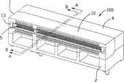
图1为本实用新型卡缘连接器的立体图。FIG. 1 is a perspective view of the card edge connector of the present invention.
图2为图1中A-A线的剖视图。Fig. 2 is a sectional view of line A-A in Fig. 1 .
图3为图1中B-B线的剖视图。Fig. 3 is a sectional view of line B-B in Fig. 1 .
图4为本实用新型卡缘连接器的部分分解图。FIG. 4 is a partially exploded view of the card edge connector of the present invention.
图5为本实用新型卡缘连接器另一角度的部分分解图。FIG. 5 is a partially exploded view of another angle of the card edge connector of the present invention.
图6为图5中点划线部分的放大图。FIG. 6 is an enlarged view of the dotted line portion in FIG. 5 .
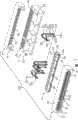
图7为本实用新型卡缘连接器的立体分解图。FIG. 7 is a three-dimensional exploded view of the card edge connector of the present invention.
图8为本实用新型卡缘连接器另一角度的立体分解图。FIG. 8 is a three-dimensional exploded view of another angle of the card edge connector of the present invention.
【具体实施方式】【Detailed ways】
请参阅图1、图4及图5所示,本实用新型卡缘连接器100用于插接电子卡(未图示),其包括绝缘本体1、设在绝缘本体1上的导电端子5、设在绝缘本体1下方的固定座2以及与绝缘本体1相配合的定位块3及抵压物4。Please refer to Fig. 1, Fig. 4 and Fig. 5, the
请参阅图7及图8所示,绝缘本体1包括上下平行的两纵长侧壁10以及位于两侧壁10间的插槽11,该插槽11用以插接电子卡,每一侧壁10上均设有若干贯穿前后且与插槽11相贯通的端子槽12,绝缘本体1在插槽11内设有一可与电子卡上的缺口相配合的挡块17,绝缘本体1的后端两侧设有一对扣槽13,绝缘本体1的后端对应挡块17位置设有第一开槽14以及位于第一开槽14上方的第二开槽16,绝缘本体1的下方设有向下凸伸的定位柱15。Please refer to Fig. 7 and Fig. 8, the
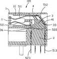
请参阅图7及图8所示,导电端子5包括第一端子51以及第二端子52。第一端子51包括收容在上方侧壁10的端子槽12内并向下突伸入插槽11的第一接触部511、自第一接触部511后端向下倾斜延伸后再向下弯折延伸的第一连接部512以及自第一连接部512下端向下竖直延伸的第一尾部513,第一接触部511排布成一排,第一连接部512及第一尾部513排布成前后两排。第二端子52包括收容在下方侧壁10的端子槽12内并向上突伸入插槽11的第二接触部521、自第二接触部521后端向后延伸后再向下弯折延伸的第二连接部522以及自第二连接部522下端向下竖直延伸的第二尾部523,第二接触部521位于第一接触部511下方并且单独排布成一排,第二连接部522及第二尾部523排布成位于对应的第一连接部512及第一尾部513前方的前后两排。第一尾部513上设有狭槽514,第二尾部523上也设有狭槽524,第一尾部513及第二尾部523均以压入配合的方式与电路板(未图示)相配合,从而与电路板形成电性连接。Please refer to FIG. 7 and FIG. 8 , the
请参阅图1至图6所示,定位块3的后端设有若干间隔设置的第一凸块31以及设置于相邻两第一凸块31之间的第一凹槽32,且第一凸块31上设有深度较第一凹槽32小的第二凹槽33,第一端子51的第一连接部512呈前后两排设置,其中,后排的第一连接部512收容在第一凸块31上的第二凹槽33内,前排的第一连接部512收容在第一凹槽32内,从而可将第一连接部512分隔开,避免第一连接部512因变形而相互接触。定位块3的前端下方设有若干间隔设置的第二凸块34以及设置于相邻两第二凸块34之间的第三凹槽35,且第二凸块34上设有深度较第三凹槽35小的第四凹槽36,第二端子52的第二连接部522呈前后两排设置,其中,后排的第二连接部522固持在第三凹槽35内,前排的第二连接部522固持在第四凹槽36内,从而可将第二连接部522分隔开,避免第二连接部522因变形而相互接触,且第二连接部522均抵压在定位块3的下方。定位块3的前端凸伸有若干卡持在端子槽12内的嵌块37以及卡持在第一开槽14内的第一卡块38,从而将定位块3更好地固定在绝缘本体1上。Please refer to Fig. 1 to Fig. 6, the rear end of the
抵压物4组装在绝缘本体1的后端,抵压物4上设有后壁41以及自后壁41向前凸伸并间隔设置的若干抵压块42,抵压物4的后壁41抵压在定位块3的第一凸块31后端,抵压块42收容在第一凹槽32内并抵压在收容在第一凹槽32内的第一连接部512,因此,抵压物4可将前后排布的第一连接部512抵压在第一凹槽32及第二凹槽33内,定位块3可将第二连接部522抵压在第三凹槽35及第四凹槽36内,从而使得抵压物4及定位块3可有效地将第一端子51的第一连接部512及第二端子52的第二连接部522维持在预定的位置上,从而可防止导电端子5的变形且可有效避免相邻的第一连接部512与第二连接部522由于过分弯折而相互抵接进而造成短路情况的发生。抵压物4的后壁41上设有若干间隔设置的狭缝43以散发第一端子51传输讯号时所产生的热量。抵压物4的前端设有一对向前延伸并与绝缘本体1上的扣槽13相配合的扣持部44以及与绝缘本体1上的第二开槽16相配合的第二卡块46,从而可以将抵压物4更好地固定在绝缘本体1上。抵压物4的下方设有向下凸伸的定位柱45。由以上可知,本实用新型的定位块3相当于抵压物抵压在第二连接部522上从而防止第二连接部522的变形。The
固定座2组装在绝缘本体1、定位块3及抵压物4的下方,从而可增加卡缘连接器100的高度,固定座2上设有可与绝缘本体1上的定位柱15以及抵压物4上的定位柱45相配合的定位孔25,从而将绝缘本体1、抵压物4及固定座2更好地固定在一起。固定座2上设有若干可供第一尾部513以及第二尾部523穿过的通孔22。The
Claims (10)
Priority Applications (2)
| Application Number | Priority Date | Filing Date | Title |
|---|---|---|---|
| CNU2008200415724UCN201252187Y (en) | 2008-08-05 | 2008-08-05 | Card edge connector |
| US12/535,848US7828560B2 (en) | 2008-08-05 | 2009-08-05 | Card edge connector having an improved spacer |
Applications Claiming Priority (1)
| Application Number | Priority Date | Filing Date | Title |
|---|---|---|---|
| CNU2008200415724UCN201252187Y (en) | 2008-08-05 | 2008-08-05 | Card edge connector |
Publications (1)
| Publication Number | Publication Date |
|---|---|
| CN201252187Ytrue CN201252187Y (en) | 2009-06-03 |
Family
ID=40747858
Family Applications (1)
| Application Number | Title | Priority Date | Filing Date |
|---|---|---|---|
| CNU2008200415724UExpired - LifetimeCN201252187Y (en) | 2008-08-05 | 2008-08-05 | Card edge connector |
Country Status (2)
| Country | Link |
|---|---|
| US (1) | US7828560B2 (en) |
| CN (1) | CN201252187Y (en) |
Cited By (1)
| Publication number | Priority date | Publication date | Assignee | Title |
|---|---|---|---|---|
| CN111834815A (en)* | 2015-09-23 | 2020-10-27 | 莫列斯有限公司 | Socket assembly |
Families Citing this family (14)
| Publication number | Priority date | Publication date | Assignee | Title |
|---|---|---|---|---|
| TWM381184U (en)* | 2009-10-30 | 2010-05-21 | T Conn Prec Corp | Improved MiniPCI connector structure |
| JP4958191B2 (en)* | 2009-11-06 | 2012-06-20 | 日本航空電子工業株式会社 | connector |
| TWM396512U (en)* | 2010-07-30 | 2011-01-11 | Tyco Electronics Holdings Bermuda No 7 Ltd | Card-edge connector |
| TWM438740U (en)* | 2011-10-28 | 2012-10-01 | Aces Electronic Co Ltd | Power connector |
| TWM438741U (en)* | 2011-10-28 | 2012-10-01 | Aces Electronic Co Ltd | Power connector |
| TWM436982U (en)* | 2011-10-28 | 2012-09-01 | Aces Electronic Co Ltd | Power connector |
| WO2017044653A1 (en)* | 2015-09-08 | 2017-03-16 | Fci Americas Technology Llc | Electrical power connector |
| TWI788394B (en)* | 2017-08-03 | 2023-01-01 | 美商安芬諾股份有限公司 | Cable assembly and method of manufacturing the same |
| WO2019195319A1 (en) | 2018-04-02 | 2019-10-10 | Ardent Concepts, Inc. | Controlled-impedance compliant cable termination |
| US11101611B2 (en) | 2019-01-25 | 2021-08-24 | Fci Usa Llc | I/O connector configured for cabled connection to the midboard |
| WO2020154507A1 (en) | 2019-01-25 | 2020-07-30 | Fci Usa Llc | I/o connector configured for cable connection to a midboard |
| CN114788097A (en) | 2019-09-19 | 2022-07-22 | 安费诺有限公司 | High speed electronic system with midplane cable connector |
| CN113258325A (en) | 2020-01-28 | 2021-08-13 | 富加宜(美国)有限责任公司 | High-frequency middle plate connector |
| US11824305B2 (en)* | 2020-09-11 | 2023-11-21 | Amphenol Commercial Products (Chengdu) Co., Ltd. | Robust and reliable high speed electrical connector assembly |
Family Cites Families (7)
| Publication number | Priority date | Publication date | Assignee | Title |
|---|---|---|---|---|
| US5980272A (en)* | 1997-10-21 | 1999-11-09 | Hon Hai Precision Ind. Co., Ltd. | Electrical connector with back shell for contact tails |
| TW505319U (en)* | 2001-12-21 | 2002-10-01 | Hon Hai Prec Ind Co Ltd | Card edge connector |
| US6887108B2 (en)* | 2002-08-01 | 2005-05-03 | Hon Hai Precision Ind. Co., Ltd. | Electrical adapter |
| CN2791918Y (en) | 2004-01-13 | 2006-06-28 | 富士康(昆山)电脑接插件有限公司 | Electric connector |
| US6884112B1 (en)* | 2004-01-30 | 2005-04-26 | Hon Hai Precision Ind. Co., Ltd. | Electrical connector having improved securing member |
| CN200959382Y (en) | 2006-09-05 | 2007-10-10 | 富士康(昆山)电脑接插件有限公司 | card edge connector |
| CN201252186Y (en)* | 2008-05-29 | 2009-06-03 | 富士康(昆山)电脑接插件有限公司 | Card edge connector |
- 2008
- 2008-08-05CNCNU2008200415724Upatent/CN201252187Y/ennot_activeExpired - Lifetime
- 2009
- 2009-08-05USUS12/535,848patent/US7828560B2/enactiveActive
Cited By (1)
| Publication number | Priority date | Publication date | Assignee | Title |
|---|---|---|---|---|
| CN111834815A (en)* | 2015-09-23 | 2020-10-27 | 莫列斯有限公司 | Socket assembly |
Also Published As
| Publication number | Publication date |
|---|---|
| US7828560B2 (en) | 2010-11-09 |
| US20100035473A1 (en) | 2010-02-11 |
Similar Documents
| Publication | Publication Date | Title |
|---|---|---|
| CN201252187Y (en) | Card edge connector | |
| CN201029143Y (en) | electrical connector | |
| US11848509B2 (en) | Electrical connector | |
| CN201130754Y (en) | electrical connector | |
| US8096815B2 (en) | Reliable electrical connection electrical connector assembly | |
| CN102354882A (en) | Electrical connector | |
| CN201576789U (en) | Card edge connector | |
| US8398422B2 (en) | Card edge connector | |
| CN201142436Y (en) | electronic card connector | |
| CN101645557A (en) | Electric connector terminal | |
| US8162680B2 (en) | Board-mounted electrical connector | |
| US7938687B2 (en) | Compact stacked card edge connector assembly | |
| US7931495B2 (en) | Stacked connectors having lower connector floatably assembled thereto | |
| CN103579811B (en) | Electric connector | |
| CN111952748B (en) | Card edge connector | |
| CN111952749B (en) | Card edge connector | |
| CN105305131B (en) | Electric connector and its manufacture method | |
| CN102801060B (en) | The manufacture method of magnetic module and the electric connector utilizing this kind of magnetic module to manufacture | |
| CN202930584U (en) | Universal Serial Bus connector | |
| CN201256230Y (en) | electrical connector | |
| CN201207450Y (en) | Connector for electronic card | |
| JP3144006U (en) | Card connector assembly | |
| CN204516949U (en) | Electric connector | |
| CN100466384C (en) | card edge connector | |
| CN201796379U (en) | electronic card |
Legal Events
| Date | Code | Title | Description |
|---|---|---|---|
| C14 | Grant of patent or utility model | ||
| GR01 | Patent grant | ||
| CX01 | Expiry of patent term | ||
| CX01 | Expiry of patent term | Granted publication date:20090603 |