CN201174415Y - Half-mode Substrate Integrated Waveguide Stereo Power Divider Using Step Transition - Google Patents
Half-mode Substrate Integrated Waveguide Stereo Power Divider Using Step TransitionDownload PDFInfo
- Publication number
- CN201174415Y CN201174415YCNU2008200337392UCN200820033739UCN201174415YCN 201174415 YCN201174415 YCN 201174415YCN U2008200337392 UCNU2008200337392 UCN U2008200337392UCN 200820033739 UCN200820033739 UCN 200820033739UCN 201174415 YCN201174415 YCN 201174415Y
- Authority
- CN
- China
- Prior art keywords
- metal
- length
- dielectric
- metal patch
- patch
- Prior art date
- Legal status (The legal status is an assumption and is not a legal conclusion. Google has not performed a legal analysis and makes no representation as to the accuracy of the status listed.)
- Expired - Fee Related
Links
Images

Landscapes
- Control Of Motors That Do Not Use Commutators (AREA)
Abstract
Translated fromChinese
Description
Translated fromChinese技术领域technical field
本实用新型属于采用阶梯过渡的半模基片集成波导立体功分器主要用于微波毫米波组件与系统的设计中,特别是一种采用阶梯过渡的半模基片集成波导立体功分器。The utility model belongs to a half-mode substrate integrated waveguide three-dimensional power divider adopting step transition, which is mainly used in the design of microwave and millimeter wave components and systems, in particular to a half-mode substrate integrated waveguide three-dimensional power divider adopting step transition.
背景技术Background technique
微波毫米波功分器在微波毫米波天线的馈线和毫米波仪表中得到了大量的应用,它是馈线系统中的一个关键部件,特别是在微波毫米波集成电路中,天线阵列的馈电需要用到低损耗、宽频带的功分器。常用的微带功分器在中心频率上它的特性较为理想,但是一旦发生频偏,整个功分器的性能都会变差,从而影响整个系统的性能。利用基片集成波导技术可以制作出高Q值、低损耗、宽频带的功率分配器,并降低加工成本和工艺难度,而在此基础上的半模基片集成波导结构更能减小其一半的体积,使其更适用于微波毫米波组件与系统的设计。Microwave and millimeter wave power dividers have been widely used in the feeder of microwave and millimeter wave antennas and millimeter wave instruments. It is a key component in the feeder system, especially in microwave and millimeter wave integrated circuits. A low-loss, wide-band power splitter is used. The commonly used microstrip power splitter has ideal characteristics at the center frequency, but once a frequency deviation occurs, the performance of the entire power splitter will deteriorate, thereby affecting the performance of the entire system. Using substrate integrated waveguide technology can produce high-Q, low-loss, wide-band power dividers, and reduce processing costs and process difficulties, and on this basis, the half-mode substrate integrated waveguide structure can reduce it by half The volume makes it more suitable for the design of microwave and millimeter wave components and systems.
实用新型内容Utility model content
本实用新型的目的在于提供一种工作在9GHz到12GHz的X波段上采用阶梯过渡的半模基片集成波导立体功分器。The purpose of the utility model is to provide a half-mode substrate integrated waveguide three-dimensional power splitter which works in the X-band of 9GHz to 12GHz and adopts step transition.
实现本实用新型目的的技术解决方案为:一种采用阶梯过渡的半模基片集成波导立体功分器,包括两排长方形金属贴片,第一排的长方形金属贴片中的第一至第六金属贴片之间互联并呈阶梯状分布,位于两端的第一、六金属贴片的两侧边沿靠边分别与第一、二锥形金属贴片的宽边连成一整体,覆于介质板的一面;第二排的长方形金属贴片中的第七至第十二金属贴片之间互联并呈阶梯状分布,一端的第十二金属贴片的边沿靠边与第三锥形金属贴片的宽边相连成一整体,覆于介质板的另一面,该第三锥形金属贴片与第二锥形金属贴片呈上下对称;所述的两排长方形金属贴片整体通过穿过介质基片的一排金属化通孔相连,并在介质板[1]的内部正中间设置金属隔板。The technical solution to realize the purpose of this utility model is: a half-mode substrate integrated waveguide three-dimensional power divider adopting a step transition, including two rows of rectangular metal patches, the first to the second row of rectangular metal patches in the first row The six metal patches are interconnected and distributed in a ladder shape. The edges on both sides of the first and sixth metal patches at both ends are respectively connected with the wide sides of the first and second tapered metal patches to form a whole, covering the dielectric board one side; the seventh to twelfth metal patches in the second row of rectangular metal patches are interconnected and distributed in a ladder shape, and the edge of the twelfth metal patch at one end is close to the edge of the third tapered metal patch The wide sides of the third tapered metal patch are connected into a whole and covered on the other side of the dielectric board. The third tapered metal patch is symmetrical up and down with the second tapered metal patch; the two rows of rectangular metal patches pass through the dielectric substrate as a whole A row of metallized through holes of the chip are connected, and a metal partition is set in the middle of the inside of the dielectric board [1].
本实用新型与现有技术相比,其显著优点为:(1)利用了矩形金属波导具有高Q值、低损耗的特点,在介质基片的基础上实现了半模基片集成波导,其工作在9GHz到12GHz的X波段上。(2)这种结构成本低廉,具有较高的Q值,较低的损耗,且工作在较宽的带宽,适用于微波毫米波集成电路的设计。(3)半模基片集成波导立体功分器的体积只有传统的基片集成波导平面功分器的四分之一,而厚度不变,更容易集成于微波毫米波组件与系统中。Compared with the prior art, the utility model has the remarkable advantages as follows: (1) Utilizes the characteristics of high Q value and low loss of the rectangular metal waveguide, realizes the half-mode substrate integrated waveguide on the basis of the dielectric substrate, and its Works on the X-band from 9GHz to 12GHz. (2) This structure is low in cost, has a high Q value, low loss, and works in a wide bandwidth, and is suitable for the design of microwave and millimeter wave integrated circuits. (3) The volume of the half-mode substrate-integrated waveguide three-dimensional power splitter is only a quarter of that of the traditional substrate-integrated waveguide planar power splitter, while the thickness remains the same, making it easier to integrate into microwave and millimeter-wave components and systems.
下面结合附图对本实用新型作进一步详细描述。Below in conjunction with accompanying drawing, the utility model is described in further detail.
附图说明Description of drawings
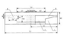
图1是根据本实用新型提出的装置的俯视图。Fig. 1 is a top view of the device proposed according to the utility model.
图2是根据本实用新型提出的装置的平视图。Fig. 2 is a plan view of the device proposed according to the utility model.
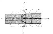
图3是本实用新型金属化通孔示意图。Fig. 3 is a schematic diagram of the metallized through hole of the present invention.
具体实施方式Detailed ways
结合图1和图2,本实用新型采用阶梯过渡的半模基片集成波导立体功分器,由内部覆有多层阶梯金属贴片的介质层和表层金属贴片组成,介质层内外各层金属贴片通过垂直的窄带金属条依次相连成一整体,且在介质层中间插入一块金属隔离板;上下金属贴片整体通过设在介质基片上的1行高度不等的金属化通孔相连,整个结构呈多层立体分布,即包括两排长方形金属贴片,第一排的长方形金属贴片中的第一至第六金属贴片2、3、4、5、6、7之间互联并呈阶梯状分布,位于两端的第一、六金属贴片2、7的两侧边沿靠边分别与第一、二锥形金属贴片8、9的宽边连成一整体,覆于介质板1的一面;第二排的长方形金属贴片中的第七至第十二金属贴片11、12、13、14、15、16之间互联并呈阶梯状分布,一端的第十二金属贴片12的边沿靠边与第三锥形金属贴片17的宽边相连成一整体,覆于介质板1的另一面,该第三锥形金属贴片17与第二锥形金属贴片9呈上下对称;所述的两排长方形金属贴片整体通过穿过介质基片2的一排金属化通孔相连,并在介质板1的内部正中间设置金属隔板10。Combining Figures 1 and 2, the utility model adopts a step-transition half-mode substrate integrated waveguide three-dimensional power splitter, which is composed of a dielectric layer covered with multi-layer stepped metal patches and a surface metal patch. The inner and outer layers of the dielectric layer The metal patches are sequentially connected into a whole through vertical narrow-band metal strips, and a metal isolation plate is inserted in the middle of the dielectric layer; the upper and lower metal patches are connected through a row of metallized through holes with different heights on the dielectric substrate. The structure is distributed in multiple layers, that is, it includes two rows of rectangular metal patches, and the first to
结合图3,本实用新型采用阶梯过渡的半模基片集成波导立体功分器,介质板1长度L1为88.5mm,宽度W2为10-12mm;金属隔板10长度L2为45-48mm,第一金属贴片2长度L5为17mm,第二至第五金属贴片3、4、5、6长度L6为3.5mm,第六金属贴片7长度L7为17.5mm,总长L3为48.5-50mm;第一至第三锥形金属贴片8、9、17的长度L4都为13.9mm,两条平行边W3和W4分别为2.4-2.6mm和1.5-1.6mm;金属化通孔到第六矩形金属贴片7远边垂直距离W1为7.2-7.5mm;第七金属贴片11的长度为37mm,宽度为10mm,介质板1厚度h为1mm,介电常数为2.2,各金属通孔高度h1、h2、h3、h4、h5、h6依次为0.5mm、0.6mm、0.7mm、0.8mm、0.9mm和1mm,金属通孔直径d为2mm,孔间距S为3.5-3.7mm。In conjunction with Fig. 3, the utility model adopts the semi-mode substrate integrated waveguide three-dimensional power divider with step transition, the length L1 of the
实施例:结合图1、图2和图3,以工作频段在9-12GHz的多层半模基片集成波导立体功分器为例,详细说明本实用新型的结构。Embodiment: With reference to Fig. 1, Fig. 2 and Fig. 3, taking a multi-layer half-mode substrate integrated waveguide three-dimensional power splitter with a working frequency band of 9-12 GHz as an example, the structure of the utility model is described in detail.
厚度h为1mm的介质板1中沿其一边插入一块长度为45mm的金属隔板10,介质板1的长度为88.5mm,介质板1的宽度为15mm,金属隔板10的宽度为10mm。介质板1内部和表层覆有由各矩形金属贴片构成的整体金属贴片(参见图2)。X轴上方的金属贴片由第一至第六金属贴片2、3、4、5、6、7及第一、二锥形金属贴片8、9和两条金属导带组成,各长方形金属贴片用z方向上等高为0.1mm、宽度为10mm的金属横条相连成一整体,各长方形金属贴片的宽度均为10mm,第一金属贴片2的长度为17mm,第二至第五金属贴片3、4、5、6的长度均为3.5mm,第六金属贴片7的长度为17.5mm,第一、二锥形贴片8、9的尺寸相同,两条平行边分别为1.5mm和4.7mm,长度为13.9mm。介质板1的另一面的金属贴片整体由第七至第十二金属贴片11、12、13、14、15、16和第三锥形金属贴片17,其中第九至第十二长方形金属贴片13、14、15、16的尺寸与第二至第五金属贴片3、4、5、6相同,第八金属贴片12的尺寸与第六金属贴片7相同,第三锥形贴片17的尺寸与第一、二锥形贴片8、9相同,第七金属贴片11的长度为37mm,宽度为10mm。位于介质板1两侧的金属贴片整体通过一行金属化通孔相连,金属孔到矩形贴片的远边距离为7.2mm,在介质平面上沿x轴方向直线分布。金属孔直径d为2mm,孔间距S为3.5mm。A
信号从左边的输入端输入,在半模基片集成波导中通过正中间的金属隔板分为两路信号,分别从上下两个输出端输出,实现等功分。我们选用的介质其介电常数为2.2,结果表明在9.2GHz-10.6GHz频段内,S11小于-20dB,两个输出端口的传输系数都接近-3dB,相对带宽接近15%。The signal is input from the input terminal on the left, and in the half-mode substrate integrated waveguide, it is divided into two signals through the metal partition in the middle, and output from the upper and lower output terminals respectively to realize equal power division. The dielectric constant of the medium we choose is 2.2. The results show that in the 9.2GHz-10.6GHz frequency band, the S11 is less than -20dB, the transmission coefficients of the two output ports are close to -3dB, and the relative bandwidth is close to 15%.
Claims (2)
Priority Applications (1)
| Application Number | Priority Date | Filing Date | Title |
|---|---|---|---|
| CNU2008200337392UCN201174415Y (en) | 2008-04-03 | 2008-04-03 | Half-mode Substrate Integrated Waveguide Stereo Power Divider Using Step Transition |
Applications Claiming Priority (1)
| Application Number | Priority Date | Filing Date | Title |
|---|---|---|---|
| CNU2008200337392UCN201174415Y (en) | 2008-04-03 | 2008-04-03 | Half-mode Substrate Integrated Waveguide Stereo Power Divider Using Step Transition |
Publications (1)
| Publication Number | Publication Date |
|---|---|
| CN201174415Ytrue CN201174415Y (en) | 2008-12-31 |
Family
ID=40201543
Family Applications (1)
| Application Number | Title | Priority Date | Filing Date |
|---|---|---|---|
| CNU2008200337392UExpired - Fee RelatedCN201174415Y (en) | 2008-04-03 | 2008-04-03 | Half-mode Substrate Integrated Waveguide Stereo Power Divider Using Step Transition |
Country Status (1)
| Country | Link |
|---|---|
| CN (1) | CN201174415Y (en) |
Cited By (3)
| Publication number | Priority date | Publication date | Assignee | Title |
|---|---|---|---|---|
| CN102904011A (en)* | 2012-10-30 | 2013-01-30 | 哈尔滨工业大学 | Balanced microstrip line transition full-mode double-ridge integrated waveguide-fed symmetrical dipole printed antenna |
| CN102904012A (en)* | 2012-10-30 | 2013-01-30 | 哈尔滨工业大学 | Combined semicircular symmetrical dipole printed antenna fed by balanced microstrip line transitional waveguide |
| CN106654543A (en)* | 2015-10-29 | 2017-05-10 | 苏州博海创业微系统有限公司 | Multilayer radiation apparatus |
- 2008
- 2008-04-03CNCNU2008200337392Upatent/CN201174415Y/ennot_activeExpired - Fee Related
Cited By (5)
| Publication number | Priority date | Publication date | Assignee | Title |
|---|---|---|---|---|
| CN102904011A (en)* | 2012-10-30 | 2013-01-30 | 哈尔滨工业大学 | Balanced microstrip line transition full-mode double-ridge integrated waveguide-fed symmetrical dipole printed antenna |
| CN102904012A (en)* | 2012-10-30 | 2013-01-30 | 哈尔滨工业大学 | Combined semicircular symmetrical dipole printed antenna fed by balanced microstrip line transitional waveguide |
| CN102904012B (en)* | 2012-10-30 | 2014-12-24 | 哈尔滨工业大学 | Combined semicircular dipole printed antenna of balance microstrip line transition waveguide feed |
| CN102904011B (en)* | 2012-10-30 | 2015-01-14 | 哈尔滨工业大学 | Balance microstrip line transition full-mode dual-ridged integrated waveguide feed dipole printed antenna |
| CN106654543A (en)* | 2015-10-29 | 2017-05-10 | 苏州博海创业微系统有限公司 | Multilayer radiation apparatus |
Similar Documents
| Publication | Publication Date | Title |
|---|---|---|
| CN105958167B (en) | Vertical substrate integration wave-guide and the vertical connecting structure including the waveguide | |
| CN106911011B (en) | An array antenna structure and design method | |
| CN201156573Y (en) | Integrated Waveguide Bandpass Filter Based on Folded Substrate | |
| CN103259072B (en) | Ultra-wideband power divider based on exponential gradient | |
| CN108777343B (en) | Substrate integrated waveguide transmission structure, antenna structure and connection method | |
| CN110212273B (en) | Dual-band duplexer based on substrate integrated waveguide | |
| CN104241737B (en) | A kind of LTCC based on resonator coupling filters balun | |
| CN204809372U (en) | Ware / combiner is divided to trisection gysel type merit | |
| CN208173765U (en) | Substrate integration wave-guide transmission structure, antenna structure | |
| CN108172958A (en) | A Periodic Slow Wave Transmission Line Unit Based on Coplanar Waveguide | |
| CN107275733A (en) | A kind of adjustable slow wave transmission line of cycle loading capacitance and short-circuit line | |
| CN201523061U (en) | Miniaturized UWB Microstrip Power Divider | |
| CN201174418Y (en) | Half-mode substrate integrated waveguide single-layer three-dimensional power divider | |
| CN103022611B (en) | A kind of wideband microband is to the vertical transition of micro-band | |
| CN201174415Y (en) | Half-mode Substrate Integrated Waveguide Stereo Power Divider Using Step Transition | |
| CN105449322B (en) | Millimeter wave double-passband filter and its design method | |
| CN2888662Y (en) | High-performance waveguide filter with integrated microwave/millimeter wave substrate | |
| CN201174416Y (en) | Substrate-integrated waveguide power splitter with step transition | |
| CN102610891B (en) | Multi-layer dual-passband coupler based on composite left and right hand folded substrate integrated waveguides | |
| CN1825677A (en) | Microwave millimeter wave substrate integrated waveguide E-plane inductive band filter | |
| CN106876855A (en) | A kind of Mini Microstrip broadband work(clutch | |
| CN108767377A (en) | A kind of commutator load phase shifter | |
| CN114171872A (en) | Broadband miniaturized millimeter wave double-channel cross bridge | |
| CN100412584C (en) | Substrate-integrated waveguide quasi-inductive window filter | |
| CN204205000U (en) | A kind of LTCC filtering Ba Lun based on resonator |
Legal Events
| Date | Code | Title | Description |
|---|---|---|---|
| C14 | Grant of patent or utility model | ||
| GR01 | Patent grant | ||
| C17 | Cessation of patent right | ||
| CF01 | Termination of patent right due to non-payment of annual fee | Granted publication date:20081231 Termination date:20100403 |