CN201130746Y - Conductive terminal - Google Patents
Conductive terminalDownload PDFInfo
- Publication number
- CN201130746Y CN201130746YCNU2007200429351UCN200720042935UCN201130746YCN 201130746 YCN201130746 YCN 201130746YCN U2007200429351 UCNU2007200429351 UCN U2007200429351UCN 200720042935 UCN200720042935 UCN 200720042935UCN 201130746 YCN201130746 YCN 201130746Y
- Authority
- CN
- China
- Prior art keywords
- conductive terminal
- contact
- extension
- terminal according
- contact portion
- Prior art date
- Legal status (The legal status is an assumption and is not a legal conclusion. Google has not performed a legal analysis and makes no representation as to the accuracy of the status listed.)
- Expired - Lifetime
Links
Images


Classifications
- H—ELECTRICITY
- H01—ELECTRIC ELEMENTS
- H01R—ELECTRICALLY-CONDUCTIVE CONNECTIONS; STRUCTURAL ASSOCIATIONS OF A PLURALITY OF MUTUALLY-INSULATED ELECTRICAL CONNECTING ELEMENTS; COUPLING DEVICES; CURRENT COLLECTORS
- H01R13/00—Details of coupling devices of the kinds covered by groups H01R12/70 or H01R24/00 - H01R33/00
- H01R13/02—Contact members
- H01R13/22—Contacts for co-operating by abutting
- H01R13/24—Contacts for co-operating by abutting resilient; resiliently-mounted
- H01R13/2464—Contacts for co-operating by abutting resilient; resiliently-mounted characterized by the contact point
- H01R13/2492—Contacts for co-operating by abutting resilient; resiliently-mounted characterized by the contact point multiple contact points
- H—ELECTRICITY
- H01—ELECTRIC ELEMENTS
- H01R—ELECTRICALLY-CONDUCTIVE CONNECTIONS; STRUCTURAL ASSOCIATIONS OF A PLURALITY OF MUTUALLY-INSULATED ELECTRICAL CONNECTING ELEMENTS; COUPLING DEVICES; CURRENT COLLECTORS
- H01R12/00—Structural associations of a plurality of mutually-insulated electrical connecting elements, specially adapted for printed circuits, e.g. printed circuit boards [PCB], flat or ribbon cables, or like generally planar structures, e.g. terminal strips, terminal blocks; Coupling devices specially adapted for printed circuits, flat or ribbon cables, or like generally planar structures; Terminals specially adapted for contact with, or insertion into, printed circuits, flat or ribbon cables, or like generally planar structures
- H01R12/70—Coupling devices
- H01R12/82—Coupling devices connected with low or zero insertion force
- H01R12/85—Coupling devices connected with low or zero insertion force contact pressure producing means, contacts activated after insertion of printed circuits or like structures
- H01R12/88—Coupling devices connected with low or zero insertion force contact pressure producing means, contacts activated after insertion of printed circuits or like structures acting manually by rotating or pivoting connector housing parts
- H—ELECTRICITY
- H01—ELECTRIC ELEMENTS
- H01R—ELECTRICALLY-CONDUCTIVE CONNECTIONS; STRUCTURAL ASSOCIATIONS OF A PLURALITY OF MUTUALLY-INSULATED ELECTRICAL CONNECTING ELEMENTS; COUPLING DEVICES; CURRENT COLLECTORS
- H01R12/00—Structural associations of a plurality of mutually-insulated electrical connecting elements, specially adapted for printed circuits, e.g. printed circuit boards [PCB], flat or ribbon cables, or like generally planar structures, e.g. terminal strips, terminal blocks; Coupling devices specially adapted for printed circuits, flat or ribbon cables, or like generally planar structures; Terminals specially adapted for contact with, or insertion into, printed circuits, flat or ribbon cables, or like generally planar structures
- H01R12/50—Fixed connections
- H01R12/51—Fixed connections for rigid printed circuits or like structures
- H01R12/55—Fixed connections for rigid printed circuits or like structures characterised by the terminals
- H01R12/57—Fixed connections for rigid printed circuits or like structures characterised by the terminals surface mounting terminals
Landscapes
- Connecting Device With Holders (AREA)
- Coupling Device And Connection With Printed Circuit (AREA)
Abstract
Description
Translated fromChinese【技术领域】【Technical field】
本实用新型关于一种导电端子,尤指一种以弹性按压方式导接晶片模块至印刷电路板的导电端子。The utility model relates to a conductive terminal, in particular to a conductive terminal for connecting a chip module to a printed circuit board in an elastic pressing manner.
【背景技术】【Background technique】
电连接器广泛应用于计算机领域,用以电性连接两个相互分离的电子元件,如晶片模组和印刷电路板,以实现两者之间的数据和信号传输。Electrical connectors are widely used in the computer field to electrically connect two separated electronic components, such as chip modules and printed circuit boards, to realize data and signal transmission between the two.
请参中国专利公告第2736971号专利所示,与本实用新型相关的电连接器一般包括绝缘本体和容设于绝缘本体中的若干导电端子,绝缘本体设有与芯片模组相对的承接面和与印刷电路板相对的安装面,贯穿承接面和安装面设有若干呈矩阵排列设置的端子收容槽。导电端子对应容设于端子收容槽中,其一端呈弹性臂向上延伸且凸出承接面以与晶片模组相应的导电垫片对接,另一端连接有锡球或者凸伸出绝缘本体的安装面以与印刷电路板电性连接。实际操作过程中,先将电连接器安装到印刷电路板,通过导电端子以实现电连接器与印刷电路板之间的电性连接,再将晶片模组置于导电端子上方,晶片模组向下驱动导电端子的弹性臂发生弯曲变形,导电端子的弹性臂借助自身的弹性而抵接于晶片模组的导电垫片上,以实现导电端子和晶片模组之间的电性连接,从而实现晶片模组与印刷电路板之间的电性导通。Please refer to the Chinese Patent Announcement No. 2736971, the electrical connector related to the utility model generally includes an insulating body and a number of conductive terminals accommodated in the insulating body, and the insulating body is provided with a receiving surface opposite to the chip module and The mounting surface opposite to the printed circuit board is provided with a plurality of terminal receiving grooves arranged in a matrix through the receiving surface and the mounting surface. The conductive terminal is correspondingly accommodated in the terminal receiving groove, one end of which is an elastic arm extending upward and protruding from the receiving surface to connect with the corresponding conductive gasket of the chip module, and the other end is connected with a solder ball or protrudes from the mounting surface of the insulating body to be electrically connected to the printed circuit board. In the actual operation process, the electrical connector is installed on the printed circuit board first, and the electrical connection between the electrical connector and the printed circuit board is realized through the conductive terminal, and then the chip module is placed on the conductive terminal, and the chip module is placed on the conductive terminal. The elastic arm of the lower driving conductive terminal is bent and deformed, and the elastic arm of the conductive terminal abuts against the conductive gasket of the chip module by virtue of its own elasticity, so as to realize the electrical connection between the conductive terminal and the chip module, thereby realizing The electrical conduction between the chip module and the printed circuit board.
为了保证电连接器信号传输的稳定性,晶片模组的导电垫片通常需要和导电端子的弹性臂可靠对接。但是,与本实用新型相关的电连接器通常存在以下缺点:导电端子一般仅设有一个弹性臂,且该弹性臂与晶片模组的导电垫片之间形成单点接触,当导电端子在安装过程中出现正位度不佳时,导电端子的弹性臂和晶片模组的导电垫片间电性导通的稳定性难以保证,从而可能导致晶片模组与印刷电路板电性连接的失效。In order to ensure the stability of signal transmission of the electrical connector, the conductive gasket of the chip module usually needs to be reliably docked with the elastic arm of the conductive terminal. However, the electrical connector related to the utility model usually has the following disadvantages: the conductive terminal is generally only provided with one elastic arm, and a single-point contact is formed between the elastic arm and the conductive gasket of the chip module. When the alignment is not good during the process, the stability of electrical conduction between the elastic arm of the conductive terminal and the conductive gasket of the chip module is difficult to ensure, which may lead to failure of the electrical connection between the chip module and the printed circuit board.
鉴于以上缺点的存在,确有必要提出一种改进的导电端子,以克服上述与本实用新型相关的电连接器中存在的缺陷和不足。In view of the above disadvantages, it is indeed necessary to propose an improved conductive terminal to overcome the above-mentioned defects and deficiencies in the electrical connector related to the utility model.
【实用新型内容】【Content of utility model】
本实用新型要解决的技术问题是提供一种导电端子,尤其是指一种能够达到与晶片模组稳定电性连接的导电端子。The technical problem to be solved by the utility model is to provide a conductive terminal, especially a conductive terminal capable of achieving stable electrical connection with a chip module.
为此,本实用新型提供了一种连接晶片模组至印刷电路板的导电端子,其包括主体部、自主体部向上延伸的延伸部,延伸部设有下延伸部和自下延伸部朝上延伸的上延伸部,其中,所述上延伸部和下延伸部的同一侧分别向上延伸设有第一接触部和第二接触部。To this end, the utility model provides a conductive terminal for connecting a chip module to a printed circuit board, which includes a main body, an extension extending upward from the main body, and the extension is provided with a lower extension and an upward extension from the lower extension. The extended upper extension part, wherein, the same side of the upper extension part and the lower extension part respectively extend upwards with a first contact part and a second contact part.
相对于与本实用新型相关的技术,本实用新型导电端子具有如下优点:自导电端子的上延伸部和下延伸部的同一侧分别向上延伸设有第一接触臂及第二接触臂,故当晶片模组置于电连接器上时,每个导电端子均可以和晶片模组下端对应的导电垫片之间形成多点接触,因此可以避免因导电端子正位度不佳而引起的导电端子和晶片模组之间接触不稳定等弊端,从而实现晶片模组和导电端子之间信号的稳定传输。Compared with the technology related to the present utility model, the conductive terminal of the present utility model has the following advantages: a first contact arm and a second contact arm are respectively extended upward from the same side of the upper extension part and the lower extension part of the conductive terminal, so when When the chip module is placed on the electrical connector, each conductive terminal can form multi-point contact with the corresponding conductive pad at the lower end of the chip module, so that the conductive terminal caused by the poor position of the conductive terminal can be avoided. There are disadvantages such as unstable contact with the chip module, so as to realize the stable transmission of signals between the chip module and the conductive terminal.
【附图说明】【Description of drawings】
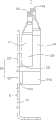
图1是本实用新型导电端子的立体图。Fig. 1 is a perspective view of the conductive terminal of the present invention.
图2是图1所示导电端子的正视图。FIG. 2 is a front view of the conductive terminal shown in FIG. 1 .
图3是图1所示导电端子的俯视图。FIG. 3 is a top view of the conductive terminal shown in FIG. 1 .
【具体实施方式】【Detailed ways】
请参图1至图3所示,本实用新型电连接器(未图示),以按压接触方式电性连接晶片模组(未图示)至印刷电路板(未图示),其包括设有端子收容槽(未图示)的绝缘本体(未图示)及收容于端子收容槽中的若干导电端子1。Please refer to Figures 1 to 3, the electrical connector (not shown) of the present utility model is used to electrically connect the chip module (not shown) to the printed circuit board (not shown) in a press-contact manner, which includes a device An insulating body (not shown) with a terminal receiving groove (not shown) and a plurality of
导电端子1设有板状的主体部11,主体部11具有长度、宽度、厚度三个方向,其中长度方向的尺寸大于宽度方向的尺寸,宽度方向的尺寸大于厚度方向的尺寸。主体部11沿长度方向的相对两侧设有凸出部111,且凸出部111与主体部11的厚度相同,该凸出部111用以与端子收容槽干涉配合从而实现导电端子1稳定地容设于绝缘本体中。凸出部111与主体部11共同形成“工”字形,且其沿插入绝缘本体的方向对称设置有倒角斜面1110,以提供导电端子1插入绝缘本体时的导向作用。The
主体部11沿其宽度方向向上延伸设有延伸部12,延伸部12包括下延伸部121及自下延伸部121朝上延伸的上延伸部122,且上延伸部122、下延伸部121及主体部11处于同一个平面。The
上延伸部122和下延伸部121的同一侧边分别向上延伸设有第一接触部13和第二接触部14,且第一接触部13的长度要小于第二接触部14。第一接触部13和第二接触部14分别于其最高点设有第一接触点130和第二接触点140,该第一接触点130和第二接触点140可分别与晶片模组下端的同一个导电垫片(未图示)电性连接。第一接触点130到主体部11的距离要小于第二接触点140到主体部11的距离,且第一接触点130的高度要小于第二接触点140的高度。第一接触部13经由第一弯曲部131和第一桥部132连接至上延伸部122,第二接触部14经由第二弯曲部141和第二桥部142连接至下延伸部121,且第一桥部132比第二桥部142更加靠近延伸部12的侧边。第一接触部13平行于第二接触部14,且两者与延伸部12均大致呈钝角设置,此种设计可方便导电端子1在模具中的成型。A
导电端子1设有连接印刷电路板的导接部15,该导接部15大致呈平板状,其下设有锡球(未图示)以电性连接晶片模组至印刷电路板。导接部15经由连接部16连接至主体部11,且与主体部11大体垂直。The
使用时,先将导电端子1插入绝缘本体中,将锡球组设于导电端子1的导接部15下端,再将容设有导电端子1的绝缘本体置于印刷电路板上,以实现导电端子1与印刷电路板的电性连接;再将晶片模组置于导电端子1上方,以实现晶片模组与导电端子1之间的电性连接,从而实现晶片模组与印刷电路板之间的电性连接。When in use, first insert the
本实用新型导电端子1延伸部12的同一侧边向上延伸设有第一接触部13和第二接触部14,第一接触部13和第二接触部14分别设有与晶片模组下端的同一导电垫片电性连接的第一接触点130和第二接触点140,故当导电端子1或晶片模组正位度不佳,产生一定的倾斜时,第一接触点130和第二接触点140中至少有一个仍能保证导电端子1与晶片模组之间良好的电性连接,从而可以实现晶片模组与印刷电路板之间稳固的电性连接。The same side of the
如上所述导电端子1的第一接触点130与第二接触点140到主体部11之间的距离设置为不相同,其也可根据实际需要设置为相同;第一接触点130与第二接触点140的高度也可设置为相同。As mentioned above, the distance between the
以上所述仅为本实用新型的优选实施方案,其它在本实施方案基础上进行的任何改进变换也应当不脱离本发明的技术方案。The above description is only the preferred embodiment of the present invention, and any other improvements and transformations based on this embodiment should not deviate from the technical solution of the present invention.
Claims (9)
Translated fromChinesePriority Applications (2)
| Application Number | Priority Date | Filing Date | Title |
|---|---|---|---|
| CNU2007200429351UCN201130746Y (en) | 2007-08-17 | 2007-08-17 | Conductive terminal |
| US12/228,973US7563105B2 (en) | 2007-08-17 | 2008-08-18 | Electrical contact having asymmetric dual-contact-engaging-arm |
Applications Claiming Priority (1)
| Application Number | Priority Date | Filing Date | Title |
|---|---|---|---|
| CNU2007200429351UCN201130746Y (en) | 2007-08-17 | 2007-08-17 | Conductive terminal |
Publications (1)
| Publication Number | Publication Date |
|---|---|
| CN201130746Ytrue CN201130746Y (en) | 2008-10-08 |
Family
ID=40018613
Family Applications (1)
| Application Number | Title | Priority Date | Filing Date |
|---|---|---|---|
| CNU2007200429351UExpired - LifetimeCN201130746Y (en) | 2007-08-17 | 2007-08-17 | Conductive terminal |
Country Status (2)
| Country | Link |
|---|---|
| US (1) | US7563105B2 (en) |
| CN (1) | CN201130746Y (en) |
Cited By (8)
| Publication number | Priority date | Publication date | Assignee | Title |
|---|---|---|---|---|
| CN105375145A (en)* | 2014-08-06 | 2016-03-02 | 第一电子工业株式会社 | Contactor and connector having the same |
| CN108736192A (en)* | 2018-04-24 | 2018-11-02 | 番禺得意精密电子工业有限公司 | Electric connector |
| CN108767520A (en)* | 2018-04-24 | 2018-11-06 | 番禺得意精密电子工业有限公司 | Electric connector |
| CN109524815A (en)* | 2017-09-18 | 2019-03-26 | 富士康(昆山)电脑接插件有限公司 | electrical connector |
| CN109713482A (en)* | 2019-02-01 | 2019-05-03 | 番禺得意精密电子工业有限公司 | Terminal group and electric connector |
| CN110311241A (en)* | 2019-06-24 | 2019-10-08 | 番禺得意精密电子工业有限公司 | Electric connector |
| CN110416789A (en)* | 2018-04-27 | 2019-11-05 | 富顶精密组件(深圳)有限公司 | Electric connector |
| CN112467438A (en)* | 2018-04-27 | 2021-03-09 | 富顶精密组件(深圳)有限公司 | Electrical connector |
Families Citing this family (26)
| Publication number | Priority date | Publication date | Assignee | Title |
|---|---|---|---|---|
| CN201207540Y (en)* | 2008-04-21 | 2009-03-11 | 富士康(昆山)电脑接插件有限公司 | Electric connector |
| TWM357747U (en)* | 2008-09-30 | 2009-05-21 | Hon Hai Prec Ind Co Ltd | Electrical connector and contacts thereof |
| TWM365563U (en)* | 2009-03-09 | 2009-09-21 | Hon Hai Prec Ind Co Ltd | Electrical connector |
| TWM375324U (en)* | 2009-06-08 | 2010-03-01 | Hon Hai Prec Ind Co Ltd | Electrical contact |
| TWM373039U (en)* | 2009-07-17 | 2010-01-21 | Hon Hai Prec Ind Co Ltd | Electrical connector and contacts thereof |
| TWM391758U (en)* | 2010-04-28 | 2010-11-01 | Hon Hai Prec Ind Co Ltd | Electrical connector |
| WO2013119533A1 (en) | 2012-02-07 | 2013-08-15 | 3M Innovative Properties Company | Board mount electrical connector |
| EP2812953A4 (en) | 2012-02-07 | 2015-10-07 | 3M Innovative Properties Co | Electrical connector contact terminal |
| US9509089B2 (en) | 2012-02-07 | 2016-11-29 | 3M Innovative Properties Company | Electrical connector latch |
| US9553401B2 (en) | 2012-02-07 | 2017-01-24 | 3M Innovative Properties Company | Electrical connector for strain relief for an electrical cable |
| US9948026B2 (en) | 2012-02-07 | 2018-04-17 | 3M Innovative Properties Company | Wire mount electrical connector |
| TWM437555U (en)* | 2012-03-07 | 2012-09-11 | Hon Hai Prec Ind Co Ltd | Terminal and electrical connector with the terminal |
| TWI583068B (en)* | 2012-08-02 | 2017-05-11 | 鴻海精密工業股份有限公司 | Electrical connector |
| CN203707414U (en)* | 2013-12-18 | 2014-07-09 | 深圳市得润电子股份有限公司 | Electric connector and conductive terminal thereof |
| TW201731603A (en)* | 2016-03-02 | 2017-09-16 | Dijiya Energy Saving Tech Inc | Lithium battery conductive connection piece and forming method thereof enabling to meet the use needs of charging and discharging of large current having high amplification factor |
| CN105938949B (en)* | 2016-05-31 | 2020-04-21 | 深圳市信维通信股份有限公司 | Rectangular impact-resistant elastic sheet connector |
| CN107492728A (en)* | 2017-01-12 | 2017-12-19 | 番禺得意精密电子工业有限公司 | Electric connector |
| CN108448284A (en)* | 2018-02-06 | 2018-08-24 | 番禺得意精密电子工业有限公司 | Electric connector |
| US10680374B2 (en)* | 2018-04-27 | 2020-06-09 | Fu Ding Precision Component (Shen Zhen) Co., Ltd. | Electrical contact |
| CN109066133A (en)* | 2018-07-10 | 2018-12-21 | 番禺得意精密电子工业有限公司 | Electric connector |
| CN111180924B (en)* | 2018-11-13 | 2024-04-16 | 泰科电子日本合同会社 | IC Socket |
| CN109713477B (en)* | 2018-11-28 | 2021-01-26 | 番禺得意精密电子工业有限公司 | Electrical connector |
| CN111262069B (en)* | 2018-11-30 | 2024-02-20 | 富顶精密组件(深圳)有限公司 | Conductive terminal |
| CN111262063B (en)* | 2018-11-30 | 2023-08-15 | 富顶精密组件(深圳)有限公司 | Conductive terminal, conductive terminal manufacturing method and terminal material belt structure |
| CN113054469B (en)* | 2019-12-26 | 2022-07-26 | 富士康(昆山)电脑接插件有限公司 | Electrical connector with improved contact arrangement |
| US12347957B2 (en)* | 2022-08-23 | 2025-07-01 | Foxconn (Kunshan) Computer Connector Co., Ltd. | Electrical connector with improved contacts |
Family Cites Families (14)
| Publication number | Priority date | Publication date | Assignee | Title |
|---|---|---|---|---|
| US5722848A (en)* | 1995-10-25 | 1998-03-03 | Hon Hai Precision Ind. Co., Ltd. | Retention mechanism for self-securement of ZIF PGA socket |
| US6371784B1 (en)* | 1999-12-02 | 2002-04-16 | The Whitaker Corporation | Zero insertion force contact for use with a pin grid array |
| JP4596638B2 (en)* | 2000-12-22 | 2010-12-08 | タイコエレクトロニクスジャパン合同会社 | Electrical connector |
| US6694609B2 (en)* | 2001-03-22 | 2004-02-24 | Molex Incorporated | Method of making stitched LGA connector |
| US6905377B2 (en)* | 2002-09-17 | 2005-06-14 | Tyco Electronics Corporation | Contact for land grid array socket |
| JP3950795B2 (en)* | 2002-10-31 | 2007-08-01 | タイコエレクトロニクスアンプ株式会社 | Socket for LGA package |
| US6805561B1 (en)* | 2003-07-22 | 2004-10-19 | Hon Hai Precision Ind. Co., Ltd. | Electrical socket having terminals with elongated mating beams |
| US7074048B2 (en)* | 2003-07-22 | 2006-07-11 | Hon Hai Precision Ind. Co., Ltd. | Land grid array socket having terminals with spring arms |
| US7156706B2 (en)* | 2003-07-22 | 2007-01-02 | Tyco Electronics Corporation | Contact having multiple contact beams |
| TWM250355U (en)* | 2003-08-22 | 2004-11-11 | Hon Hai Prec Ind Co Ltd | Electrical connector |
| CN100470964C (en)* | 2005-12-27 | 2009-03-18 | 富士康(昆山)电脑接插件有限公司 | Electric connector |
| CN2917029Y (en)* | 2006-03-14 | 2007-06-27 | 富士康(昆山)电脑接插件有限公司 | electrical connector |
| TWI336544B (en)* | 2006-06-05 | 2011-01-21 | Hon Hai Prec Ind Co Ltd | Electrical connector |
| US7357665B1 (en)* | 2007-06-14 | 2008-04-15 | Cheng Uei Precision Industry Co., Ltd. | Battery connector |
- 2007
- 2007-08-17CNCNU2007200429351Upatent/CN201130746Y/ennot_activeExpired - Lifetime
- 2008
- 2008-08-18USUS12/228,973patent/US7563105B2/ennot_activeExpired - Fee Related
Cited By (13)
| Publication number | Priority date | Publication date | Assignee | Title |
|---|---|---|---|---|
| CN105375145A (en)* | 2014-08-06 | 2016-03-02 | 第一电子工业株式会社 | Contactor and connector having the same |
| US10998677B2 (en) | 2017-09-18 | 2021-05-04 | Foxconn Interconnect Technology Limited | Electrical connector transmitting high frequency signals |
| CN109524815A (en)* | 2017-09-18 | 2019-03-26 | 富士康(昆山)电脑接插件有限公司 | electrical connector |
| CN108767520A (en)* | 2018-04-24 | 2018-11-06 | 番禺得意精密电子工业有限公司 | Electric connector |
| CN108736192A (en)* | 2018-04-24 | 2018-11-02 | 番禺得意精密电子工业有限公司 | Electric connector |
| CN110416789A (en)* | 2018-04-27 | 2019-11-05 | 富顶精密组件(深圳)有限公司 | Electric connector |
| CN112467438A (en)* | 2018-04-27 | 2021-03-09 | 富顶精密组件(深圳)有限公司 | Electrical connector |
| CN110416789B (en)* | 2018-04-27 | 2022-07-26 | 富顶精密组件(深圳)有限公司 | Electrical connector with improved contact arrangement |
| CN109713482A (en)* | 2019-02-01 | 2019-05-03 | 番禺得意精密电子工业有限公司 | Terminal group and electric connector |
| CN109713482B (en)* | 2019-02-01 | 2021-05-25 | 番禺得意精密电子工业有限公司 | Terminal group and electric connector |
| CN110311241A (en)* | 2019-06-24 | 2019-10-08 | 番禺得意精密电子工业有限公司 | Electric connector |
| CN111555058A (en)* | 2019-06-24 | 2020-08-18 | 番禺得意精密电子工业有限公司 | Electrical connector |
| US11011862B2 (en) | 2019-06-24 | 2021-05-18 | Lotes Co., Ltd | Electrical connector |
Also Published As
| Publication number | Publication date |
|---|---|
| US20090047817A1 (en) | 2009-02-19 |
| US7563105B2 (en) | 2009-07-21 |
Similar Documents
| Publication | Publication Date | Title |
|---|---|---|
| CN201130746Y (en) | Conductive terminal | |
| US7264486B2 (en) | Electrical connector | |
| CN201097410Y (en) | electrical connector terminal | |
| CN1295361A (en) | Electric connector | |
| CN101212098A (en) | Electrical connector terminal | |
| CN101212093B (en) | electrical connector terminal | |
| CN100470964C (en) | Electric connector | |
| US7367814B2 (en) | Electrical contacts used in an electrical connector | |
| US9130321B2 (en) | Electrical connector having contact for either BGA or LGA package | |
| CN201142393Y (en) | electrical connector | |
| CN201160146Y (en) | electrical connector terminal | |
| US8690585B2 (en) | Electrical connector for low profile application | |
| CN201549675U (en) | Electrical connectors and their conductive terminals | |
| CN201549747U (en) | Electric connector component | |
| CN101227040B (en) | Electric connector terminal | |
| CN207765649U (en) | A kind of conducting terminal and electric connector | |
| CN101227034B (en) | Electric connector terminal | |
| CN100429833C (en) | Electric connector | |
| CN201041915Y (en) | electrical connector | |
| CN201130744Y (en) | electrical connector terminal | |
| CN201438550U (en) | electrical connector terminal | |
| CN201498014U (en) | electronic card | |
| CN2454917Y (en) | Electronic-card connector | |
| CN201122698Y (en) | Electric connector | |
| CN201142386Y (en) | electrical connector |
Legal Events
| Date | Code | Title | Description |
|---|---|---|---|
| C14 | Grant of patent or utility model | ||
| GR01 | Patent grant | ||
| CX01 | Expiry of patent term | Granted publication date:20081008 | |
| CX01 | Expiry of patent term |