CN201117941Y - electrical connector - Google Patents
electrical connectorDownload PDFInfo
- Publication number
- CN201117941Y CN201117941YCNU2007200454226UCN200720045422UCN201117941YCN 201117941 YCN201117941 YCN 201117941YCN U2007200454226 UCNU2007200454226 UCN U2007200454226UCN 200720045422 UCN200720045422 UCN 200720045422UCN 201117941 YCN201117941 YCN 201117941Y
- Authority
- CN
- China
- Prior art keywords
- base
- cover
- electrical connector
- chip module
- elastic arm
- Prior art date
- Legal status (The legal status is an assumption and is not a legal conclusion. Google has not performed a legal analysis and makes no representation as to the accuracy of the status listed.)
- Expired - Fee Related
Links
Images


Classifications
- H—ELECTRICITY
- H01—ELECTRIC ELEMENTS
- H01R—ELECTRICALLY-CONDUCTIVE CONNECTIONS; STRUCTURAL ASSOCIATIONS OF A PLURALITY OF MUTUALLY-INSULATED ELECTRICAL CONNECTING ELEMENTS; COUPLING DEVICES; CURRENT COLLECTORS
- H01R12/00—Structural associations of a plurality of mutually-insulated electrical connecting elements, specially adapted for printed circuits, e.g. printed circuit boards [PCB], flat or ribbon cables, or like generally planar structures, e.g. terminal strips, terminal blocks; Coupling devices specially adapted for printed circuits, flat or ribbon cables, or like generally planar structures; Terminals specially adapted for contact with, or insertion into, printed circuits, flat or ribbon cables, or like generally planar structures
- H01R12/70—Coupling devices
- H01R12/82—Coupling devices connected with low or zero insertion force
- H01R12/85—Coupling devices connected with low or zero insertion force contact pressure producing means, contacts activated after insertion of printed circuits or like structures
- H01R12/89—Coupling devices connected with low or zero insertion force contact pressure producing means, contacts activated after insertion of printed circuits or like structures acting manually by moving connector housing parts linearly, e.g. slider
- H—ELECTRICITY
- H01—ELECTRIC ELEMENTS
- H01R—ELECTRICALLY-CONDUCTIVE CONNECTIONS; STRUCTURAL ASSOCIATIONS OF A PLURALITY OF MUTUALLY-INSULATED ELECTRICAL CONNECTING ELEMENTS; COUPLING DEVICES; CURRENT COLLECTORS
- H01R12/00—Structural associations of a plurality of mutually-insulated electrical connecting elements, specially adapted for printed circuits, e.g. printed circuit boards [PCB], flat or ribbon cables, or like generally planar structures, e.g. terminal strips, terminal blocks; Coupling devices specially adapted for printed circuits, flat or ribbon cables, or like generally planar structures; Terminals specially adapted for contact with, or insertion into, printed circuits, flat or ribbon cables, or like generally planar structures
- H01R12/50—Fixed connections
- H01R12/51—Fixed connections for rigid printed circuits or like structures
- H01R12/55—Fixed connections for rigid printed circuits or like structures characterised by the terminals
- H01R12/57—Fixed connections for rigid printed circuits or like structures characterised by the terminals surface mounting terminals
- H—ELECTRICITY
- H01—ELECTRIC ELEMENTS
- H01R—ELECTRICALLY-CONDUCTIVE CONNECTIONS; STRUCTURAL ASSOCIATIONS OF A PLURALITY OF MUTUALLY-INSULATED ELECTRICAL CONNECTING ELEMENTS; COUPLING DEVICES; CURRENT COLLECTORS
- H01R12/00—Structural associations of a plurality of mutually-insulated electrical connecting elements, specially adapted for printed circuits, e.g. printed circuit boards [PCB], flat or ribbon cables, or like generally planar structures, e.g. terminal strips, terminal blocks; Coupling devices specially adapted for printed circuits, flat or ribbon cables, or like generally planar structures; Terminals specially adapted for contact with, or insertion into, printed circuits, flat or ribbon cables, or like generally planar structures
- H01R12/70—Coupling devices
- H01R12/71—Coupling devices for rigid printing circuits or like structures
- H01R12/712—Coupling devices for rigid printing circuits or like structures co-operating with the surface of the printed circuit or with a coupling device exclusively provided on the surface of the printed circuit
- H01R12/716—Coupling device provided on the PCB
Landscapes
- Connecting Device With Holders (AREA)
- Coupling Device And Connection With Printed Circuit (AREA)
Abstract
Translated fromChinese
Description
Translated fromChinese【技术领域】【Technical field】
本实用新型涉及一种电连接器,尤指一种电性连接芯片模组至电路板的电连接器。The utility model relates to an electric connector, in particular to an electric connector for electrically connecting a chip module to a circuit board.
【背景技术】【Background technique】
ZIF(Zero Insertion Force)电连接器(即通常所称的零插入力电连接器)广泛地应用于计算机系统中,以将芯片模组电性连接至电路板。现有技术揭示了多种ZIF电连接器,如美国专利公告6623298号、6508658号、6471536号以及中国专利公告CN2520033、CN2520588、CN2520013等。ZIF电连接器一般包括基体、可动组接在基体上的盖体以及收容于基体与盖体之间以驱动盖体自一开启位置向一闭合位置滑动的驱动装置,其中基体中设有若干收容有导电端子的端子收容槽,盖体上对应基体上端子收容槽的位置开设有若干通孔。ZIF电连接器在电性连接芯片模组至电路板时,芯片模组置于盖体上方,芯片模组的针脚穿过盖体上的通孔并伸入到端子收容槽之中;当盖体处于开启位置时,芯片模组的针脚未与导电端子电性接触,当盖体在驱动装置的带动下由开启位置向闭合位置运动时,芯片模组的针脚亦向某一方向移动,并最终与导电端子达成良好的电性接触,从而电连接器与芯片模组之间建立起电性连接。现有技术同样揭示了多种应用于ZIF电连接器的导电端子,如中国专利公告CN2537140、CN2537141、CN2519451、CN2523053、CN2458763等。ZIF (Zero Insertion Force) electrical connectors (commonly known as zero insertion force electrical connectors) are widely used in computer systems to electrically connect chip modules to circuit boards. The prior art discloses various ZIF electrical connectors, such as US Patent No. 6623298, No. 6508658, and No. 6471536, and Chinese Patent No. CN2520033, CN2520588, and CN2520013. ZIF electrical connectors generally include a base body, a cover movably assembled on the base body, and a drive device accommodated between the base body and the cover body to drive the cover body to slide from an open position to a closed position, wherein the base body is provided with several The terminal accommodating groove for accommodating the conductive terminal is provided with a plurality of through holes on the cover corresponding to the position of the terminal accommodating groove on the base body. When the ZIF electrical connector electrically connects the chip module to the circuit board, the chip module is placed above the cover, and the pins of the chip module pass through the through holes on the cover and extend into the terminal receiving groove; when the cover When the cover is in the open position, the pins of the chip module are not in electrical contact with the conductive terminals. When the cover moves from the open position to the closed position driven by the driving device, the pins of the chip module also move in a certain direction, and Finally, a good electrical contact is achieved with the conductive terminal, so that an electrical connection is established between the electrical connector and the chip module. The prior art also discloses a variety of conductive terminals applied to ZIF electrical connectors, such as Chinese patent announcements CN2537140, CN2537141, CN2519451, CN2523053, CN2458763 and so on.
但是,上述电连接器至少存在以下缺陷,导电端子通常需要设置一对弹性臂,以在芯片模组的针脚移动后夹持芯片模组的针脚,进而达成电性连接,这样的设计的不利之处是,导电端子的结构比较复杂且对电连接器的端子收容槽的容置空间要求较高,不利于导电端子的密集排列,进而不能适应电连接器小型化发展趋势的要求。However, the above-mentioned electrical connector has at least the following defects. The conductive terminals usually need to be provided with a pair of elastic arms to clamp the pins of the chip module after the pins of the chip module move to achieve electrical connection. The disadvantage of such a design The disadvantage is that the structure of the conductive terminals is relatively complex and requires a relatively high accommodating space for the terminal receiving groove of the electrical connector, which is not conducive to the dense arrangement of the conductive terminals, and thus cannot meet the requirements of the development trend of miniaturization of the electrical connector.
鉴于上述状况,确有必要提供一种改进的电连接器,以克服现有技术的电连接器存在的缺陷。In view of the above situation, it is necessary to provide an improved electrical connector to overcome the defects of the prior art electrical connectors.
【实用新型内容】【Content of utility model】
本实用新型要解决的技术问题是提供一种电连接器,其能够适应电连接器小型化发展趋势的要求。The technical problem to be solved by the utility model is to provide an electrical connector, which can meet the requirements of the miniaturization development trend of the electrical connector.
为解决上述技术问题,本实用新型提供一种电连接器,可电性连接芯片模组至电路板,包括基体、可动地组接于基体上方的盖体,以及一组导电端子,其中基体对应设有一组端子收容槽以收容导电端子,盖体对应基体上的端子收容槽设有一组通孔,所述导电端子设有延伸于端子收容槽侧壁间的弹性臂,芯片模组组接至盖体的上方,芯片模组的针脚穿过盖体上的通孔并插入到端子收容槽之中,当盖体相对于基体沿某一方向作动时,芯片模组的针脚在盖体的带动下移动同时压迫导电端子的弹性臂,弹性臂受力后产生作用于针脚上的法向力,所述法向力使弹性臂与针脚紧密接触,所述法向力的方向与针脚的移动方向相反。In order to solve the above technical problems, the utility model provides an electrical connector, which can electrically connect the chip module to the circuit board, including a base, a cover movably assembled above the base, and a set of conductive terminals, wherein the base Correspondingly, a group of terminal receiving grooves are provided to accommodate the conductive terminals, and the cover body is provided with a group of through holes corresponding to the terminal receiving grooves on the substrate. To the top of the cover, the pins of the chip module pass through the through holes on the cover and are inserted into the terminal receiving groove. When the cover is moved in a certain direction relative to the base, the pins of the chip module are on the cover Driven by the force, the elastic arm of the conductive terminal is moved and pressed at the same time. After the elastic arm is stressed, a normal force acting on the pin is generated. The normal force makes the elastic arm closely contact with the pin. The direction of the normal force is the same as that of the pin. Move in the opposite direction.
与相关技术相比,本实用新型的电连接器具有以下优点:首先,导电端子可以具有简单的结构,如只设置一个弹性臂即可;其次,通常导电端子的弹性臂与端子收容槽的侧壁间需要预留有可供导电端子的弹性臂变形的空间,而芯片模组的针脚在插入本实用新型的电连接器的端子收容槽之后正向压迫导电端子,所述针脚是朝向上述预留空间移动,因此,能够有效利用空间,进而能够适应电连接器小型化的发展趋势。Compared with related technologies, the electrical connector of the present utility model has the following advantages: first, the conductive terminal can have a simple structure, such as only one elastic arm is provided; Space for the deformation of the elastic arm of the conductive terminal needs to be reserved between the walls, and the pins of the chip module positively press the conductive terminal after being inserted into the terminal receiving groove of the electrical connector of the present invention. Therefore, the space can be effectively used and the development trend of miniaturization of electrical connectors can be adapted.
【附图说明】【Description of drawings】
图1是本实用新型电连接器与芯片模组的示意图,其中芯片模组尚未组接至电连接器。FIG. 1 is a schematic diagram of an electrical connector and a chip module of the present invention, wherein the chip module has not yet been assembled to the electrical connector.
图2是本实用新型电连接器与芯片模组的示意图,显示了芯片模组已组设至电连接器,但其针脚尚未与导电端子的弹性臂接触时的状态。Fig. 2 is a schematic diagram of the electrical connector and the chip module of the present invention, showing the state when the chip module has been assembled to the electrical connector, but its pins are not in contact with the elastic arms of the conductive terminals.
图3是本实用新型电连接器与芯片模组的示意图,显示了盖体作动后带动芯片模组的针脚与导电端子的弹性臂产生接触的情形。FIG. 3 is a schematic diagram of the electrical connector and the chip module of the present invention, showing the contact between the pins of the chip module and the elastic arms of the conductive terminals after the cover is actuated.
【具体实施方式】【Detailed ways】
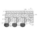
如图1至图3所示,本实用新型关于一种电连接器1,可用以承载芯片模组2并电性连接芯片模组2至印刷电路板(未图示),进而使芯片模组2与印刷电路板之间能够传递信号及电流。As shown in Figures 1 to 3, the utility model relates to an
电连接器1包括基体10、盖体14及收容于基体10中的一组导电端子12,其中基体10设有对接面100,对接面100上设有一组端子收容槽102以收容对应的导电端子12。The
盖体14可动地组设于基体10上,其设有与基体10对接面100相对的下表面140及与下表面140相对的上表面142,贯穿上表面142及下表面140设有一组与端子收容槽102对应的通孔146,这些通孔146可供芯片模组2的针脚20穿过,并且通孔146在靠近上表面142处设置有倒角形成的导引槽(未标号),以方便芯片模组2的针脚20插入通孔146。The
基体10与盖体14之间还可设置一驱动装置(未图示),如同现有技术的ZIF型连接器,该驱动装置可为驱动杆或者偏心凸轮,可驱动盖体14相对于基体10滑动,此种设计为公众熟知。A driving device (not shown) can also be arranged between the
导电端子12分别容置于对应的端子收容槽102中,导电端子12设有固持于端子收容槽102内的基部120、自基部120一侧延伸而出的弹性臂122,以及设于基部120下端的焊接部124。弹性臂122先沿远离基部120的方向延伸,弯折后沿靠近基部120的方向延伸,所述弹性臂122还可以是自基部120的顶端(未标号,靠近盖体14的一端)延伸而出;所述焊接部124自基部120延伸出端子收容槽102后贴在基体10的下表面(未标号)上,并且与弹性臂122分别置于基部120的两侧,当然焊接部124与弹性臂122可以设计成在基部120的同一侧。The
芯片模组2设有一组针脚20,芯片模组2可安装至盖体14的上表面142,所述针脚20可穿过对应的通孔146。The
请参考图2及图3,当芯片模组2组接至电连接器1时,芯片模组2置于盖体14上,所述针脚20穿过盖体14上的通孔146并且插入到端子收容槽102中,最初针脚20并不与导电端子12的弹性臂122接触,此时,盖体14的位置通常称作开启位置;芯片模组2的针脚20插入到端子收容槽102中后,操作驱动装置,使盖体14相对于基体10滑动。盖体14沿某一方向作动后,芯片模组2的针脚20在盖体14的带动下沿相同方向(如图3中箭头X所示方向)移动,具体的讲,针脚20朝向导电端子12的弹性臂122移动,同时压迫弹性臂122;弹性臂122受力后相应地产生作用于针脚20上的一法向力Fn及一轴向力Ft,其中法向力Fn的方向与针脚20的移动方向相反并且使弹性臂122与针脚20紧密接触,而所述轴向力Ft方向向下,有助于芯片模组2更紧地贴在盖体14上。特别地,法向力Fn的方向或者针脚20的移动方向也能够垂直于导电端子12的基部120时,导电端子12对容置空间的需求将进一步降低。Please refer to FIG. 2 and FIG. 3, when the
综上所述,本实用新型电连接器1的导电端子12可以具有简单的结构,如只设置一个弹性臂122即可;其次,由于导电端子12的弹性臂122与端子收容槽102的侧壁间本身需要预留有可供导电端子12的弹性臂122变形的空间,而芯片模组2的针脚20在插入端子收容槽102之后采取正向压迫导电端子12的接触方式,使针脚20朝向上述预留空间移动,因此,能够有效利用空间,进而能够适应电连接器小型化的发展趋势。In summary, the
Claims (7)
Translated fromChinesePriority Applications (2)
| Application Number | Priority Date | Filing Date | Title |
|---|---|---|---|
| CNU2007200454226UCN201117941Y (en) | 2007-08-21 | 2007-08-21 | electrical connector |
| US12/229,373US7661976B2 (en) | 2007-08-21 | 2008-08-21 | Electrical connector having improved electrical connection between contacts and pins of the package for minimizing the connector |
Applications Claiming Priority (1)
| Application Number | Priority Date | Filing Date | Title |
|---|---|---|---|
| CNU2007200454226UCN201117941Y (en) | 2007-08-21 | 2007-08-21 | electrical connector |
Publications (1)
| Publication Number | Publication Date |
|---|---|
| CN201117941Ytrue CN201117941Y (en) | 2008-09-17 |
Family
ID=39992529
Family Applications (1)
| Application Number | Title | Priority Date | Filing Date |
|---|---|---|---|
| CNU2007200454226UExpired - Fee RelatedCN201117941Y (en) | 2007-08-21 | 2007-08-21 | electrical connector |
Country Status (2)
| Country | Link |
|---|---|
| US (1) | US7661976B2 (en) |
| CN (1) | CN201117941Y (en) |
Cited By (4)
| Publication number | Priority date | Publication date | Assignee | Title |
|---|---|---|---|---|
| CN102437446A (en)* | 2010-05-11 | 2012-05-02 | 泰科电子公司 | Socket connector assembly with compressive contacts |
| CN102809879A (en)* | 2011-05-31 | 2012-12-05 | 中强光电股份有限公司 | Projection device |
| CN110112595A (en)* | 2019-05-07 | 2019-08-09 | 番禺得意精密电子工业有限公司 | Electric connector and electric connector combination |
| US11512873B2 (en) | 2017-02-14 | 2022-11-29 | Valeo Systemes Thermiques | Electrical connection interface of an electric heating device for a motor vehicle |
Families Citing this family (10)
| Publication number | Priority date | Publication date | Assignee | Title |
|---|---|---|---|---|
| US8938876B2 (en) | 2010-05-06 | 2015-01-27 | Advanced Micro Devices, Inc. | Method of mounting a circuit board |
| US8837162B2 (en) | 2010-05-06 | 2014-09-16 | Advanced Micro Devices, Inc. | Circuit board socket with support structure |
| US8292631B2 (en)* | 2010-11-16 | 2012-10-23 | Hon Hai Precision Ind. Co., Ltd. | Low profile electrical connector |
| US8425246B1 (en)* | 2011-12-01 | 2013-04-23 | Advanced Micro Devices, Inc. | Low profile semiconductor device socket |
| US8939778B2 (en)* | 2013-01-10 | 2015-01-27 | Hon Hai Precision Industry Co., Ltd. | Electrcial socket with LGA type coil contacts for IC package |
| DE102013209435A1 (en)* | 2013-05-22 | 2014-11-27 | Robert Bosch Gmbh | Plug connection with an optimized to avoid chips guide element |
| CN106797098B (en)* | 2014-09-26 | 2020-10-16 | 英特尔公司 | Socket contact technology and construction |
| US10617302B2 (en) | 2016-07-07 | 2020-04-14 | Masimo Corporation | Wearable pulse oximeter and respiration monitor |
| US11272839B2 (en) | 2018-10-12 | 2022-03-15 | Ma Simo Corporation | System for transmission of sensor data using dual communication protocol |
| CN113036479B (en)* | 2019-12-09 | 2025-09-16 | 富士康(昆山)电脑接插件有限公司 | Electric connector, electric connector combination and lock catch assembly thereof |
Family Cites Families (17)
| Publication number | Priority date | Publication date | Assignee | Title |
|---|---|---|---|---|
| US3854788A (en)* | 1973-02-28 | 1974-12-17 | Itt | Electrical connector assembly |
| US3918784A (en)* | 1974-06-05 | 1975-11-11 | Amp Inc | Miniature connector for circuit component |
| US4052117A (en)* | 1975-10-20 | 1977-10-04 | A P Products Incorporated | Integrated circuit socket |
| US4420215A (en)* | 1979-12-26 | 1983-12-13 | A P Products Incorporated | Variable effective length cantilever contact and connector |
| US4410231A (en)* | 1981-09-08 | 1983-10-18 | Texas Instruments Incorporated | Integrated circuit mounting socket |
| US4637670A (en)* | 1984-04-23 | 1987-01-20 | Amp Incorporated | Dual in-line package carrier assembly |
| JPH02123086U (en)* | 1989-03-22 | 1990-10-09 | ||
| JP3406180B2 (en)* | 1997-04-21 | 2003-05-12 | ヒロセ電機株式会社 | Intermediate electrical connector |
| US6200141B1 (en)* | 1997-08-19 | 2001-03-13 | Aries Electronics, Inc. | Land grid array connector |
| JP2002025731A (en)* | 2000-07-07 | 2002-01-25 | Texas Instr Japan Ltd | Socket and electronic component mounting device |
| JP4845304B2 (en)* | 2000-10-25 | 2011-12-28 | 株式会社センサータ・テクノロジーズジャパン | Socket and electronic component mounting apparatus including the same |
| US6383007B1 (en)* | 2001-08-27 | 2002-05-07 | Hon Hai Precision Ind. Co., Ltd. | ZIF socket assembly with improved protector |
| US6702594B2 (en)* | 2001-12-14 | 2004-03-09 | Hon Hai Precision Ind. Co., Ltd. | Electrical contact for retaining solder preform |
| TW539289U (en)* | 2002-06-28 | 2003-06-21 | Hon Hai Prec Ind Co Ltd | Electrical connector |
| JP4551189B2 (en)* | 2003-12-26 | 2010-09-22 | タイコエレクトロニクスジャパン合同会社 | PGA type IC socket |
| US7147489B1 (en)* | 2005-10-12 | 2006-12-12 | Tai Twun Enterprise Co., Ltd. | Socket having a structure for grasping solder balls |
| US7318736B1 (en)* | 2006-08-08 | 2008-01-15 | Sensata Technologies, Inc. | Burn-in sockets for BGA IC devices having an integrated slider with full ball grid compatibility |
- 2007
- 2007-08-21CNCNU2007200454226Upatent/CN201117941Y/ennot_activeExpired - Fee Related
- 2008
- 2008-08-21USUS12/229,373patent/US7661976B2/ennot_activeExpired - Fee Related
Cited By (5)
| Publication number | Priority date | Publication date | Assignee | Title |
|---|---|---|---|---|
| CN102437446A (en)* | 2010-05-11 | 2012-05-02 | 泰科电子公司 | Socket connector assembly with compressive contacts |
| CN102809879A (en)* | 2011-05-31 | 2012-12-05 | 中强光电股份有限公司 | Projection device |
| US11512873B2 (en) | 2017-02-14 | 2022-11-29 | Valeo Systemes Thermiques | Electrical connection interface of an electric heating device for a motor vehicle |
| CN110112595A (en)* | 2019-05-07 | 2019-08-09 | 番禺得意精密电子工业有限公司 | Electric connector and electric connector combination |
| CN110112595B (en)* | 2019-05-07 | 2020-10-30 | 番禺得意精密电子工业有限公司 | Electrical connector and electrical connector combination |
Also Published As
| Publication number | Publication date |
|---|---|
| US7661976B2 (en) | 2010-02-16 |
| US20090053914A1 (en) | 2009-02-26 |
Similar Documents
| Publication | Publication Date | Title |
|---|---|---|
| CN201117941Y (en) | electrical connector | |
| CN201130746Y (en) | Conductive terminal | |
| CN102084553B (en) | FPC connector for electrically connecting FPC to PCB and FPC connection method using same | |
| CN101237107B (en) | Electric connector | |
| CN201797112U (en) | electrical connector | |
| CN201112691Y (en) | Electrical connector and electrical connector assembly using such electrical connector | |
| CN201130801Y (en) | electrical connector | |
| CN101212093B (en) | electrical connector terminal | |
| CN201041909Y (en) | Electric connector | |
| CN101237106B (en) | Electric connector | |
| CN201266708Y (en) | Electric connector terminal | |
| CN201576807U (en) | Electric connector | |
| CN201181770Y (en) | Electronic device | |
| CN101640360A (en) | Electric connector | |
| CN2706902Y (en) | Electric connector | |
| CN114824865B (en) | FFC interface pitch conversion connector | |
| CN101577382B (en) | Electric connector terminal | |
| CN201549747U (en) | Electric connector component | |
| CN101227040B (en) | Electric connector terminal | |
| CN223308241U (en) | BTB test seat | |
| CN213816476U (en) | PCBA B2B Connector switching structure | |
| CN201323338Y (en) | Cable connector component | |
| CN211126139U (en) | Flexible circuit substrate assembly, circuit substrate assembly and connector plugging tool | |
| CN201112742Y (en) | electrical connector terminal | |
| CN2520012Y (en) | Board to board connector |
Legal Events
| Date | Code | Title | Description |
|---|---|---|---|
| C14 | Grant of patent or utility model | ||
| GR01 | Patent grant | ||
| CF01 | Termination of patent right due to non-payment of annual fee | Granted publication date:20080917 Termination date:20150821 | |
| EXPY | Termination of patent right or utility model |