CN201066499Y - Touch control panel structure - Google Patents
Touch control panel structureDownload PDFInfo
- Publication number
- CN201066499Y CN201066499YCNU2006201665164UCN200620166516UCN201066499YCN 201066499 YCN201066499 YCN 201066499YCN U2006201665164 UCNU2006201665164 UCN U2006201665164UCN 200620166516 UCN200620166516 UCN 200620166516UCN 201066499 YCN201066499 YCN 201066499Y
- Authority
- CN
- China
- Prior art keywords
- substrate
- panel structure
- touch panel
- light
- conductor
- Prior art date
- Legal status (The legal status is an assumption and is not a legal conclusion. Google has not performed a legal analysis and makes no representation as to the accuracy of the status listed.)
- Expired - Lifetime
Links
- 239000000758substrateSubstances0.000claimsabstractdescription58
- 239000004020conductorSubstances0.000claimsabstractdescription50
- 230000008859changeEffects0.000abstractdescription9
- 230000006698inductionEffects0.000abstractdescription5
- 230000008878couplingEffects0.000abstractdescription3
- 238000010168coupling processMethods0.000abstractdescription3
- 238000005859coupling reactionMethods0.000abstractdescription3
- 239000000853adhesiveSubstances0.000description10
- 230000001070adhesive effectEffects0.000description8
- 239000012212insulatorSubstances0.000description8
- 239000000463materialSubstances0.000description7
- 230000009471actionEffects0.000description6
- 238000000034methodMethods0.000description5
- 229920002120photoresistant polymerPolymers0.000description5
- 238000000576coating methodMethods0.000description4
- 238000010586diagramMethods0.000description4
- 238000005516engineering processMethods0.000description4
- 239000011248coating agentSubstances0.000description3
- 238000005530etchingMethods0.000description3
- AMGQUBHHOARCQH-UHFFFAOYSA-Nindium;oxotinChemical compound[In].[Sn]=OAMGQUBHHOARCQH-UHFFFAOYSA-N0.000description3
- 239000004973liquid crystal related substanceSubstances0.000description3
- 239000004033plasticSubstances0.000description3
- 229920006267polyester filmPolymers0.000description3
- 230000008569processEffects0.000description3
- 238000004544sputter depositionMethods0.000description3
- 238000006243chemical reactionMethods0.000description2
- 239000010432diamondSubstances0.000description2
- 230000000694effectsEffects0.000description2
- 239000011521glassSubstances0.000description2
- PCHJSUWPFVWCPO-UHFFFAOYSA-NgoldChemical compound[Au]PCHJSUWPFVWCPO-UHFFFAOYSA-N0.000description2
- 229910052737goldInorganic materials0.000description2
- 239000010931goldSubstances0.000description2
- 229920000515polycarbonatePolymers0.000description2
- 239000004417polycarbonateSubstances0.000description2
- 238000007639printingMethods0.000description2
- 229910052709silverInorganic materials0.000description2
- 239000004332silverSubstances0.000description2
- QNRATNLHPGXHMA-XZHTYLCXSA-N(r)-(6-ethoxyquinolin-4-yl)-[(2s,4s,5r)-5-ethyl-1-azabicyclo[2.2.2]octan-2-yl]methanol;hydrochlorideChemical compoundCl.C([C@H]([C@H](C1)CC)C2)CN1[C@@H]2[C@H](O)C1=CC=NC2=CC=C(OCC)C=C21QNRATNLHPGXHMA-XZHTYLCXSA-N0.000description1
- 229910000838Al alloyInorganic materials0.000description1
- -1ITO)Chemical compound0.000description1
- BQCADISMDOOEFD-UHFFFAOYSA-NSilverChemical compound[Ag]BQCADISMDOOEFD-UHFFFAOYSA-N0.000description1
- 238000003491arrayMethods0.000description1
- 238000000151depositionMethods0.000description1
- 230000008021depositionEffects0.000description1
- 229910003460diamondInorganic materials0.000description1
- 238000006073displacement reactionMethods0.000description1
- 230000005611electricityEffects0.000description1
- 239000000835fiberSubstances0.000description1
- 238000012905input functionMethods0.000description1
- 230000000873masking effectEffects0.000description1
- 230000007246mechanismEffects0.000description1
- 239000012811non-conductive materialSubstances0.000description1
- 229920001690polydopaminePolymers0.000description1
- 230000035945sensitivityEffects0.000description1
- 230000003068static effectEffects0.000description1
- 239000012780transparent materialSubstances0.000description1
Images


Landscapes
- Switches That Are Operated By Magnetic Or Electric Fields (AREA)
Abstract
Description
Translated fromChinese技术领域technical field
本实用新型涉及一种触控板结构,尤其指一种可提供游标移动与使用者输入或其它应用的装置。The utility model relates to a touch panel structure, in particular to a device that can provide cursor movement and user input or other applications.
背景技术Background technique
触控板可提供电子装置各种输入功能,从模拟实体按键或滚动键到复杂模式或动作的识别系统,例如:美国第5,880,411专利揭示了一种优越移动特性或动作识别的触控板。Touchpads can provide various input functions for electronic devices, ranging from simulating physical keys or scroll keys to recognition systems for complex patterns or actions. For example, US Patent No. 5,880,411 discloses a touchpad with superior movement characteristics or action recognition.
然而,有许多应用欲显示触控板的底面所呈现的影像,例如:该触控板可覆盖(或称堆迭)于一液晶显示器或阴极射线管(Cathode Ray Tube,CRT)屏幕来产生图形使用者界面(Graphical User Interface,GUI)的效果;或者,其它应用可能也想显示触控板的底面以显示静态信息,例如:提示广告信息或导引使用者输入的图样;但前面所述的现有技术或举例对这个问题的解决都还有欠缺。However, there are many applications that want to display the image presented on the bottom surface of the touch panel. For example, the touch panel can be overlaid (or stacked) on a liquid crystal display or a cathode ray tube (Cathode Ray Tube, CRT) screen to generate graphics. The effect of the user interface (Graphical User Interface, GUI); or, other applications may also want to display the bottom surface of the touchpad to display static information, such as: prompting advertising information or guiding user input patterns; but the aforementioned The prior art or examples all have a lack of solutions to this problem.
此外,由于现有电容式触控板例如:美国第5,457,289、4,806,709、4,733,222号专利各有其未解决的缺点,例如:美国第5,457,289号专利案必须前装防护罩、第4,806,709号专利需要一致的导电面;因此,有必要针对现有技术的缺点加以改善。In addition, due to the existing capacitive touch panels such as: U.S. Patent Nos. 5,457,289, 4,806,709, and 4,733,222 each have their unresolved shortcomings, for example: U.S. Patent No. Conductive surface; therefore, it is necessary to improve the shortcomings of the prior art.
实用新型内容Utility model content
本实用新型要解决的问题是提供一种触控板结构,本实用新型的主要目的,是利用触控板结构受物体接触时产生电学特性的变化而达到控制光源明灭的作用。The problem to be solved by the utility model is to provide a touch panel structure. The main purpose of the utility model is to use the touch panel structure to control the light source by changing the electrical characteristics when it is touched by an object.
本实用新型的另一目的,是运用控制光源明灭的技术,指示使用者该触控板结构是否处于可用状态或其界定范围的输入灵活度。Another purpose of the present invention is to use the technology of controlling the light source to indicate whether the touch panel structure is in a usable state or the input flexibility of the defined range.
为达到上述目的,本实用新型的一种触控板结构形成于多个基底,用来提供一传导性物体接触,该触控板结构主要包括以下构件布置堆迭层叠而成:一第一基底,其一侧设有一导光层;及一第二基底,承载有电路且设有第一导体而形成感应轨迹,在所述第一基底的至少一侧粘附有接合层介于所述第一基底与导光层之间,所述导光板的周围可设至少一发光元件且连接所述第二基底的电路,所述第二基底的电路通过接收触控板结构受所述物体接触时导致该感应轨迹的耦合电容量变化,来判断该物体的接触并因此控制所述发光元件的明灭。In order to achieve the above purpose, a touch panel structure of the present invention is formed on multiple substrates to provide a conductive object contact. The touch panel structure mainly includes the following components arranged and stacked: a first substrate , one side of which is provided with a light guide layer; and a second base, which carries a circuit and is provided with a first conductor to form a sensing track, and at least one side of the first base is adhered with a bonding layer interposed between the first Between a base and the light guide layer, at least one light-emitting element may be arranged around the light guide plate and connected to the circuit of the second base, and the circuit of the second base receives the contact of the touch panel structure The coupling capacitance of the sensing track is changed to judge the contact of the object and thus control the light-emitting element to turn on and off.
与现有技术相比,本实用新型具有以下优点:Compared with the prior art, the utility model has the following advantages:
本实用新型可以利用触控板结构受物体接触时产生电学特性的变化而达成控制光源明灭的作用,而且可以运用控制光源明灭的技术,指示使用者该触控板结构是否处于可用状态或其界定范围的输入灵活度。The utility model can use the change of electrical characteristics of the touch panel structure to achieve the function of controlling the light source when it is touched by an object, and can use the technology of controlling the light source to indicate whether the touch panel structure is in a usable state or its limit Range input flexibility.
附图说明Description of drawings
图1是本实用新型的触控板结构的一种可行应用模式示意图;Fig. 1 is a schematic diagram of a feasible application mode of the touch panel structure of the present utility model;
图2是本实用新型的触控板结构的一种可行实施例的侧面示意图;Fig. 2 is a schematic side view of a possible embodiment of the touch panel structure of the present invention;
图3是本实用新型的触控板结构的一种可行应用模式示意图;Fig. 3 is a schematic diagram of a feasible application mode of the touch panel structure of the present invention;
图4是本实用新型的触控板结构的一种可行应用模式示意图;Fig. 4 is a schematic diagram of a feasible application mode of the touch panel structure of the present invention;
图5至图7是触控板结构的第一导体的一种可行布局示意图;5 to 7 are schematic diagrams of a possible layout of the first conductor of the touch panel structure;
图8至图13是本实用新型触控板结构的另一种可行实施例的侧面示意图。8 to 13 are schematic side views of another possible embodiment of the structure of the touch panel of the present invention.
主要元件符号说明如下:The main component symbols are explained as follows:
1感应系统1 induction system
11触控板结构11 Touchpad structure
11A1第一基底11A1 First base
11A2第二基底11A2 second substrate
11A3第三基底11A3 third base
11A4第四基底11A4 fourth base
11B粘着剂11B adhesive
11C第一导体11C first conductor
11C1X轴感应轨迹11C1X-axis induction track
11C2Y轴感应轨迹11C2Y-axis induction track
11C′第二导体11C' second conductor
11D作动层11D action layer
11E菱形11E diamond
11F绝缘体11F insulator
11G涂层11G coating
11H电介质11H Dielectric
11J导光层11J light guide layer
11L发光元件11L light emitting element
11′接合层11' bonding layer
12处理器12 processors
121输入单元121 input unit
122运算单元122 computing units
123向量处理单元123 vector processing units
具体实施方式Detailed ways
对于本实用新型的优点、目的、技术特征及功效,通过以下配合附图的本案较佳实施案例加以详细说明。The advantages, purposes, technical features and effects of the present utility model are described in detail through the following preferred implementation examples of this case with accompanying drawings.
参照图1(可配合参照其它各图),显示应用本实用新型的触控板结构11作为其感应单元的一触控感应系统1的一种可行应用模式(图中显示应用于触控感应系统1)。前述触控感应系统1,主要包括:一触控板结构11,可感测(或称侦测、感知)物体O(例如:手指、触控笔stylus等具有传导性的物体,配合参照图3、图4,但不以此为限)接近或触及(以下称接触)而产生电容量变化,即,上述物体可导致在前述触控板结构11所设的至少一感应轨迹(或称感应图形sensor trace,参照下述)的电容变化;一处理器12,连接前述触控板结构11,通过接收(或称读取)该电容量变化来判断该物体的接触或/和其在触控板结构11上的位置,但不以此为限。With reference to Fig. 1 (other figures can be referred to in conjunction), it shows a feasible application mode of a touch sensing system 1 using the
上述处理器12可进一步包括有:一输入单元121,可存取前述电容量变化的信息;一运算单元122,连接该输入单元121,可将前述电容量变化的信息数字化;一向量处理单元123,连接该运算单元122,通过处理所述数字化后的信息(简称数字化信息)而获得一物体O(配合参照图3、图4)接触该触控板结构11的位置信息,而前述位置信息可供搭配本实用新型触控板结构11的其它装置或系统(例如:计算机、手机、PDA等或/和其显示屏,但不以此为限)利用,例如作为该装置或系统的输入/输出(I/O)设备,所述输入单元121、运算单元122、向量处理单元123也可具有抑制噪声的作用,以此排除由触控板结构11所感应而来的噪声。The above-mentioned
在一可行的实施模式中,上述感应轨迹可提供充分电容来耦合前述物体O,该感应轨迹可为导体所组成细线(但不以此为限)而被绘制于所述触控板结构11预设提供物体O接触的位置,配合参照图2(也可配合参照其它各图),其中触控板结构11主要包括有如下述堆迭而成的构件(但不以此为限):一第一基底11A1,至少顶面透光且绝缘,可用透光且绝缘的一粘着剂11B来粘附其它涂有可透光的一第一导体11C或/和可透光、绝缘的一第二基底11A2。In a feasible implementation mode, the above-mentioned sensing track can provide sufficient capacitance to couple the aforementioned object O, and the sensing track can be drawn on the
上述第一导体11C一般可利用一喷溅程序或由一印刷方式而沉积于前述第二基底11A2上;该第一导体11C欲形成透光的感应轨迹的布局则可通过一光阻剂和蚀刻过程而达成,或者,第一导体11C也可由喷溅或有选择性地印刷涂布一负型图层而覆盖该第二基底11A2,然后,去除负型图层即可留下适当透光感应轨迹的图样。The above-mentioned
上述第一基底11A1、第二基底11A2可为聚酯薄膜(polyester film)、玻璃(glass)、聚碳酸酯纤维塑料(polycarbonate plastic)、麦拉(Myler)等(但不以此为限)可透光材料,但不以此为限(例如:第二基底11A2也可为非透光材料);前述可透光、绝缘的粘着剂11B可为例如:3M#8142、467等,但不以此为限;可透光导体11C例如:氧化锡铟(Indium Tin Oxide,ITO)、透明导电性塑料、银、金、铝合金等,但不以此为限。具有该项技术领域常识者应该可理解,因没有材料是完全透明的,为增加感应单元11的透明度,可行方式例如有:第一,基底11A1、11A2和粘着剂11B可选择有近似或相同的折射率,通过前述极小化不同构件的折射率来使光通过材料的变形作用(或称扭曲作用)减到最小而增加透明度;第二,运用美国第5,880,411所述的感应技术,可容许高输出阻抗,因此,可透光导体11C的阻抗系数可相对较高且平稳,该阻抗系数譬如300OMEGA./square(但不以此为限),提高可透光导体11C的透明度。The first substrate 11A1 and the second substrate 11A2 can be polyester film, glass, polycarbonate plastic, Myler, etc. (but not limited thereto). Light-transmitting material, but not limited thereto (for example: the second substrate 11A2 can also be non-light-transmitting material); the aforementioned light-transmitting, insulating adhesive 11B can be, for example: 3M#8142, 467, etc., but not in This is the limit; the light-
一作动层11D,可堆迭于第一基底11A1或第二基底11A2的一侧且为可通过看穿基底11A1、11A2而显示的位置,该作动层11D例如:一个透光或不透光的基底,或一影像显示装置如液晶显示(Liquid Crystal Display,LCD)器、阴极射线管(Cathode Ray Tube,CRT)、指纹辨识器、电路板等(但不以此为限);在一可行的实施例中,作动层11D也可完全省略,或第二基底11A2也可能被省略且导体11C可直接布局在作动层11D;此外,第一基底11A1、第二基底11A2的堆迭位置可互换而没有减损其性能,此外,只要第一基底11A1是绝缘且自粘于第一导体11C,则粘着剂11B可能被排除或省略。前述所谓“自黏”例如:可透光、绝缘的第一基底11A1披覆有透光涂层。An
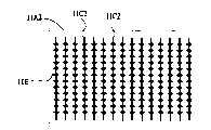
配合参照图5或图6(可配合参照其它各图)显示一维的触控感应系统1的可行实施例,不仅可侦测出上述物体O接触,也可侦测第一导体11C所布局的感应轨迹阵列的方向的一前述物体O的位置,前述物体O的位置可通过测量该第一导体11C所布局的感应轨迹阵列的电容值而计算,且根据物体O覆盖而耦合所述感应轨迹电容量的增减变化来计算物体O的位置所在,上述处理器12可根据存取前述物体O位置的连续历史资料来估计该物体O沿感应轨迹阵列的移动,且/或可整合抑制由所述触控板结构11感应的噪声的机制或结构。Cooperating with reference to FIG. 5 or FIG. 6 (coordinated with reference to other figures) shows a feasible embodiment of the one-dimensional touch sensing system 1, which can not only detect the contact of the above-mentioned object O, but also detect the layout of the
一维的触控感应系统1的触控板结构11包括有多个的感应轨迹沿一个指定的轴而等距间隔布置而形成阵列,可因此达到物体位移(包括位置或移动等)的充分辨识率,各感应轨迹的间隔可被设计为便于上述物体O覆盖在触控板结构11所预设供物体O接触的感应区的任一特定位置的至少二感应轨迹,提高前述感应轨迹密度或较高精确度的A/D转换(也即所述信息的数字化,可通过上述处理器12来达成)可增加触控感应系统1计算前述物体O位置的解析度。The
如先前在图2所描述,但不以此为限的实施模式中,上述基底11A1或/且11A2均匀地涂以透光第一导体11C,且前述第一导体11C所形成的感应轨迹阵列被使用一光阻剂和蚀刻过程而完成布局。或者,以负型光阻布局而形成的图层也可披覆该透光第一基底11A1或第二基底11A2,例如透光第一导体11C先以一喷溅程序或由一涂覆的方法被沉积于第一基底11A1、第二基底11A2上,经光罩及蚀刻后除去负型光阻图层而留下感应轨迹阵列。As previously described in FIG. 2 , but not limited thereto, the substrate 11A1 or/and 11A2 is evenly coated with a light-transmitting
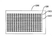
配合参照图3、图5(可配合参考其它各图),显示一些感应轨迹阵列用来计算在触控板结构11中X轴(即X轴感应轨迹11C1阵列)的位置的一个可行实施模式,各感应轨迹可为透光导体、等距间隔呈菱形11E的阵列般设在透光、绝缘的第一基底11A1(第二基底11A2也为可行的模式),可增加感应轨迹的范围且让菱形区的图样包括无导电性材料的区域。With reference to FIG. 3 and FIG. 5 (other figures may be referred to in conjunction), a feasible implementation mode for calculating the position of the X-axis (that is, the X-axis sensing track 11C1 array) in the
配合参照图3、图6(可配合参照其它各图),相当于一些感应轨迹阵列用来计算在触控板结构11中Y轴(即Y轴感应轨迹11C2阵列)的位置的一个可行实施模式,各感应轨迹11C2可为透光导体、等距间隔呈菱形11E的阵列般设在透光、绝缘的第二基底11A2,可增加感应轨迹的范围且让菱形区的图样包括无导电性材料的区域。With reference to Fig. 3 and Fig. 6 (other figures can be referred to in conjunction), it is equivalent to a feasible implementation mode in which some sensing track arrays are used to calculate the position of the Y-axis (ie, the Y-axis sensing track 11C2 array) in the
配合参照图4、图7(可配合参照其它各图),是一个象征二维触控感应系统1的附图(整合有图5、图6所示的感应轨迹阵列也为一可行的模式),该触控感应系统1可测定所述物体O存在或出现,例如沿二个方向轴(为说明起见,以下简称X轴或Y轴)的上述物体O位置。Cooperate with reference to FIG. 4 and FIG. 7 (you can refer to other figures together), which is a drawing symbolizing the two-dimensional touch sensing system 1 (integrating the sensing track array shown in FIG. 5 and FIG. 6 is also a feasible mode) , the touch sensing system 1 can determine the presence or appearance of the object O, for example, the position of the object O along two direction axes (for illustration, hereinafter referred to as X axis or Y axis).
上述感应轨迹阵列的实际数量和触控板结构11两个轴(X轴或Y轴)的存在将取决于一个特定系统或装置的感应区和辨识率的要求,为达到充分位置辨识率,各感应轨迹的间隔一般可被设计成便于上述物体O遮蔽在感应区的各轴(X轴、Y轴)的任一个预定位置中至少两感应轨迹。The actual number of the above-mentioned sensing track array and the presence of two axes (X-axis or Y-axis) of the
前述图6(可配合参照其它各图),是触控板结构11的从第二基底11A2以Y轴感应轨迹阵列在上面且X轴感应轨迹由第一基底11A1在底部的一仰视图,用至少一透光第一导体11C层填装整个感应区是适合的,该第一透光导体11C材料,例如:氧化锡铟(Indium Tin Oxide,ITO)、金、银等(但不以此为限)。The aforementioned FIG. 6 (other figures can be referred to in conjunction with each other) is a bottom view of the
于一可行的实施模式中,该图8(可配合参照其它各图),二维的触控板结构11显示的堆迭组合可按顺序颠倒而没有减损其功能,X轴透光、绝缘的第一基底11A1是供物体O接触的顶面,前述第一基底11A1的一侧是透光的X轴感应轨迹11C1,细薄、透光、较佳粘着性的绝缘体11F分隔X轴感应轨迹11C1与Y轴感应轨迹11C2;与X轴感应轨迹11C1相似,Y轴感应轨迹11C2是披覆于透光、绝缘的第二基底11A2的一侧。In a feasible implementation mode, in this FIG. 8 (you can refer to other figures together), the stacked combination displayed by the two-dimensional
已描述于图2的透光基底11A1、11A2、粘着剂11B绝缘体11F和X轴感应轨迹11C1和Y轴感应轨迹11C2等技术皆同样适用于二维的触控板结构11。The transparent substrates 11A1 , 11A2 , the
在一可行的实施模式中,可利用一电子防护罩(图中未描述)隔绝感应轨迹与从触控感应系统1的电子电路所感应的电噪声;此外,配合参照图9显示在二维的触控板结构11的第一基底11A1、第二基底11A2与图8所描述者可为相同技术,在第一基底11A1下,其它层透光绝缘体11F附加于另一可透光第二导体11C′和一第三基底11A3,不同于第一导体11C所构成的X轴感应轨迹11C1和Y轴感应轨迹11C2,该第二导体11C′可为接地的均匀导体层,因此提供感测单元11电子防护,避免受噪声的影响或干扰,而适合为导体11C′和基底11A3的材料的例子可如图2中所描述的可透光或非透光材料,在此不再描述。In a feasible implementation mode, an electronic shield (not shown in the figure) can be used to isolate the sensing track from the electrical noise induced by the electronic circuit of the touch sensing system 1; The first base 11A1 and the second base 11A2 of the
该第二导体11C′或/和基底11A3也可被插入在基底11A2和作动层11D之间,也即使用导体11C′和基底11A3来增加一透明接地板也可适用于显示在图2中该堆迭的一维的触控板结构11。The
请参照图10(可配合参照其它各图)显示一触控感应系统1的二维的触控板结构11的一可行的实施模式,一可透光基底11A1可使用透光绝缘体11F粘合透光的第一导体11C,可如同在图2所显示,该第一导体11C包括的X轴感应轨迹11C1阵列布局且涂在第二基底11A2的一侧;在前述第二基底11A2另一侧可布局且涂有透光导体11C所包括的Y轴感应轨迹11C2阵列;一第四基底11A4以透光绝缘体11F粘合透光第一导体11C(可为Y感应轨迹11C2阵列),该可行的实施模式是当菱形感应轨迹11C1或/和感应轨迹11C2排列在第二基底11A2时,由于考虑到可减少误差第二基底11A2是用透光的第一导体11C披覆在其两侧,由于第二基底11A2包括两导体X轴感应轨迹11C1、Y轴感应轨迹11C2阵列对准可能发生在以光阻剂布局轨迹阵列的蚀刻/沉积之前,可大幅简化X和Y感应轨迹布局的图案对准(或称校准)误差。Please refer to FIG. 10 (with reference to other figures) which shows a feasible implementation mode of a two-dimensional
前述透光、绝缘的基底11A1、11A2、11A4也可适用于二维或一维的触控板结构11,另外,就电子防护而言,该透光的第四基底11A4可用如在图9所显示的第二导体11C′和第一基底11A1来替换。The aforementioned light-transmitting and insulating substrates 11A1, 11A2, and 11A4 are also applicable to the two-dimensional or one-dimensional
增加上述感应轨迹密度,使一支细尖的导电性触控笔也可电容耦合至少二感应轨迹,或者,增加A/D转换的精确度(也即所述信息的数字化,可通过上述处理器12来达成)可提升侦测在感应轨迹(导体X轴感应轨迹11C1或/和感应轨迹11C2阵列)上片刻电容变化的灵敏度。Increase the density of the above-mentioned sensing tracks, so that a fine-point conductive stylus can also capacitively couple at least two sensing tracks, or increase the accuracy of A/D conversion (that is, digitization of the information can be achieved through the above-mentioned processor 12) can improve the sensitivity of detecting momentary capacitance changes on the sensing traces (conductor X-axis sensing traces 11C1 and/or the array of sensing traces 11C2).
参照图11(可配合参照其它各图)显示一触控感应系统1的触控板结构11的另一可行的实施模式,关于二维感测单元11的各层堆迭大致与前述各图相同,其中第一基底11A1的一侧披覆有粗线条、具阻抗、可透光的涂层11G,可用来延伸一支细尖的导电性触控笔的有效接触范围。Referring to FIG. 11 (other figures may be referred to together) shows another feasible implementation mode of the
参照图12(可配合参照其它各图),显示堆迭组合的触控板结构11的一可行实施模式,第一基底11A1、第二基底11A2相同于前述各图所描述的二维的触控板结构11,主要的差异是第一基底11A1、第二基底11A2具弹性或/和可挠性,例如:聚酯薄膜(polyester film)等,但不以此为限,在第二基底11A2下是可透光绝缘体11F粘附一透光、可挠电介质层11H,其他层绝缘体11F分别粘附前述电介质层11H、可透光第一导体11C(X轴感应轨迹11C1或/和Y轴感应轨迹11C2)、第三基底11A3,该第三基底11A3可利用刚性材料制成,所述刚性材料例如:玻璃、聚碳酸酯纤维塑料等或/和其所制成的电路板,但不以此为限,第二导体11C′可为电子接地的透光均匀导体层。Referring to FIG. 12 (other figures may be referred to together), a feasible implementation mode of the stacked and combined
综合上述,该第一基底11A1可作为光反射层,于所述第一基底11A1的一侧可增设一导光层11J(图中未描述),而第二基底11A2可作为承载有电路的电路板或/和设有第一导体11C(X轴感应轨迹11C1或/和Y轴感应轨迹11C2),在上述第一基底11A1的至少一侧可粘附有接合层11′(例如:前述粘着剂11B或绝缘体11F),其中一接合层11′介于前述第一基底11A1与导光层11J之间;此外,该导光层11J的周围(例如在第一基底11A1和/或第二基底11A2的侧边或下方等)可设至少一发光元件11L(图中未描述)且连接所述第二基底11A2的电路或上述处理器12,用来让使用者触压前述导光层11J而迫使该第一基底11A1或/和接合层接触第一导体11C(X轴感应轨迹11C1或/和Y轴感应轨迹11C2)而产生电容量变化,第二基底11A2的电路或/和上述处理器12可接收前述电容量变化值而控制该发光元件11L的明灭,通过第一基底11A1反射或/和透过所述导光层11J折射出前述发光元件11L的光线,而达到提示使用者该触控板结构11的位置及范围的功效,并且,所述第二基底11A2的电路与上述处理器12可整合于一起或分离。To sum up the above, the first substrate 11A1 can be used as a light reflection layer, a light guiding layer 11J (not shown in the figure) can be added on one side of the first substrate 11A1, and the second substrate 11A2 can be used as a circuit carrying a circuit The plate or/and is provided with a first conductor 11C (X-axis sensing track 11C1 or/and Y-axis sensing track 11C2), and at least one side of the first substrate 11A1 can be adhered with a bonding layer 11' (for example: the aforementioned adhesive 11B or insulator 11F), wherein a bonding layer 11' is interposed between the first base 11A1 and the light guide layer 11J; in addition, the surroundings of the light guide layer 11J (for example, on the first base 11A1 and/or the second base 11A2 at least one light-emitting element 11L (not shown in the figure) and connected to the circuit of the second substrate 11A2 or the above-mentioned processor 12, which is used to allow the user to touch the aforementioned light-guiding layer 11J to force The first substrate 11A1 or/and the bonding layer contact the first conductor 11C (the X-axis sensing track 11C1 or/and the Y-axis sensing track 11C2) to produce a capacitance change, and the circuit of the second substrate 11A2 or/and the above-mentioned processor 12 can The lighting of the light-emitting element 11L is controlled by receiving the capacitance change value, and the light of the light-emitting element 11L is reflected by the first substrate 11A1 or/and refracted through the light guide layer 11J to remind the user that the touch panel The position and scope of the structure 11, and the circuit of the second substrate 11A2 and the processor 12 can be integrated together or separated.
以上公开的仅为本实用新型的几个具体实施例,但是,本实用新型并非局限于此,任何本领域的技术人员能思之的变化都应落入本实用新型的保护范围。The above disclosures are only a few specific embodiments of the utility model, but the utility model is not limited thereto, and any changes conceivable by those skilled in the art should fall within the protection scope of the utility model.
Claims (8)
Translated fromChinesePriority Applications (1)
| Application Number | Priority Date | Filing Date | Title |
|---|---|---|---|
| CNU2006201665164UCN201066499Y (en) | 2006-12-07 | 2006-12-07 | Touch control panel structure |
Applications Claiming Priority (1)
| Application Number | Priority Date | Filing Date | Title |
|---|---|---|---|
| CNU2006201665164UCN201066499Y (en) | 2006-12-07 | 2006-12-07 | Touch control panel structure |
Publications (1)
| Publication Number | Publication Date |
|---|---|
| CN201066499Ytrue CN201066499Y (en) | 2008-05-28 |
Family
ID=39483681
Family Applications (1)
| Application Number | Title | Priority Date | Filing Date |
|---|---|---|---|
| CNU2006201665164UExpired - LifetimeCN201066499Y (en) | 2006-12-07 | 2006-12-07 | Touch control panel structure |
Country Status (1)
| Country | Link |
|---|---|
| CN (1) | CN201066499Y (en) |
Cited By (1)
| Publication number | Priority date | Publication date | Assignee | Title |
|---|---|---|---|---|
| TWI474244B (en)* | 2011-10-14 | 2015-02-21 | Egalax Empia Technology Inc | System and method for communication through touch screens |
- 2006
- 2006-12-07CNCNU2006201665164Upatent/CN201066499Y/ennot_activeExpired - Lifetime
Cited By (1)
| Publication number | Priority date | Publication date | Assignee | Title |
|---|---|---|---|---|
| TWI474244B (en)* | 2011-10-14 | 2015-02-21 | Egalax Empia Technology Inc | System and method for communication through touch screens |
Similar Documents
| Publication | Publication Date | Title |
|---|---|---|
| JP4929319B2 (en) | Capacitive touch screen or touchpad for fingers or stylus | |
| US8564314B2 (en) | Capacitive touch sensor for identifying a fingerprint | |
| EP1138014B1 (en) | A flexible transparent touch sensing system for electronic devices | |
| KR101352117B1 (en) | Display device having touch panel and touch sensing method thereof | |
| US20150042908A1 (en) | Touch panel and touch display apparatus | |
| EP3796141B1 (en) | Merged floating pixels in a touch screen | |
| US20080185193A1 (en) | Touch pad structure | |
| TWI394067B (en) | Multi - sensor touchpad | |
| US8119937B2 (en) | Capacitive touch panel | |
| CN101836178A (en) | Touch screen or touchpad with single-touch or multi-touch capability comprising an array of pressure sensors and fabrication of such sensors | |
| US8154673B2 (en) | Touch panel and driving method thereof | |
| KR101274945B1 (en) | Projected capacitive touch panel and method for manufacturing the same | |
| JP2009129100A (en) | Touch pad for double work | |
| JP2014093088A (en) | Touch screen panel and portable electronic apparatus having the same | |
| JP3130570U (en) | Touch panel structure | |
| US20150177871A1 (en) | Touch panel, manufacturing method thereof, and touchscreen apparatus | |
| CN202495007U (en) | touch pad | |
| US20090223723A1 (en) | Capacitive touch panel | |
| CN101430618A (en) | Electronic device with multiple touch characteristics and multi-mode touch screen thereof | |
| CN201066499Y (en) | Touch control panel structure | |
| US10306758B2 (en) | Enhanced conductors | |
| US20140062915A1 (en) | Touchscreen panel and touchscreen device | |
| TW202004437A (en) | Touch sensing apparatus | |
| Phares | Capacitive Touchscreen Technology | |
| KR101655431B1 (en) | 3 dimension touch screen panel |
Legal Events
| Date | Code | Title | Description |
|---|---|---|---|
| C14 | Grant of patent or utility model | ||
| GR01 | Patent grant | ||
| CX01 | Expiry of patent term | Granted publication date:20080528 | |
| EXPY | Termination of patent right or utility model |