CN1992232A - Method of manufacturing eeprom device - Google Patents
Method of manufacturing eeprom deviceDownload PDFInfo
- Publication number
- CN1992232A CN1992232ACNA200610170170XACN200610170170ACN1992232ACN 1992232 ACN1992232 ACN 1992232ACN A200610170170X ACNA200610170170X ACN A200610170170XACN 200610170170 ACN200610170170 ACN 200610170170ACN 1992232 ACN1992232 ACN 1992232A
- Authority
- CN
- China
- Prior art keywords
- gate
- forming
- layer
- cell
- mask pattern
- Prior art date
- Legal status (The legal status is an assumption and is not a legal conclusion. Google has not performed a legal analysis and makes no representation as to the accuracy of the status listed.)
- Granted
Links
- 238000004519manufacturing processMethods0.000titleclaimsabstractdescription8
- 125000006850spacer groupChemical group0.000claimsabstractdescription41
- 238000000034methodMethods0.000claimsabstractdescription29
- 239000004065semiconductorSubstances0.000claimsabstractdescription16
- 239000000758substrateSubstances0.000claimsabstractdescription15
- 238000005468ion implantationMethods0.000claimsdescription6
- 239000010410layerSubstances0.000description56
- 238000005530etchingMethods0.000description10
- 238000000151depositionMethods0.000description9
- 230000008021depositionEffects0.000description6
- 238000001312dry etchingMethods0.000description4
- 230000003287optical effectEffects0.000description3
- 239000011229interlayerSubstances0.000description2
- 238000002955isolationMethods0.000description2
- 238000012986modificationMethods0.000description2
- 230000004048modificationEffects0.000description2
- 150000004767nitridesChemical class0.000description2
- 238000007254oxidation reactionMethods0.000description2
- 229910021420polycrystalline siliconInorganic materials0.000description2
- 229920005591polysiliconPolymers0.000description2
- 229910052710siliconInorganic materials0.000description2
- 239000010703siliconSubstances0.000description2
- VYPSYNLAJGMNEJ-UHFFFAOYSA-NSilicium dioxideChemical compoundO=[Si]=OVYPSYNLAJGMNEJ-UHFFFAOYSA-N0.000description1
- 230000015556catabolic processEffects0.000description1
- 239000004020conductorSubstances0.000description1
- 238000006731degradation reactionMethods0.000description1
- 239000002019doping agentSubstances0.000description1
- 239000011810insulating materialSubstances0.000description1
- 230000003647oxidationEffects0.000description1
- 238000000059patterningMethods0.000description1
- 230000000149penetrating effectEffects0.000description1
- 238000000206photolithographyMethods0.000description1
- 229910052814silicon oxideInorganic materials0.000description1
- 230000007704transitionEffects0.000description1
- 238000010977unit operationMethods0.000description1
Images


Classifications
- H—ELECTRICITY
- H10—SEMICONDUCTOR DEVICES; ELECTRIC SOLID-STATE DEVICES NOT OTHERWISE PROVIDED FOR
- H10B—ELECTRONIC MEMORY DEVICES
- H10B43/00—EEPROM devices comprising charge-trapping gate insulators
- H10B43/30—EEPROM devices comprising charge-trapping gate insulators characterised by the memory core region
- H—ELECTRICITY
- H10—SEMICONDUCTOR DEVICES; ELECTRIC SOLID-STATE DEVICES NOT OTHERWISE PROVIDED FOR
- H10D—INORGANIC ELECTRIC SEMICONDUCTOR DEVICES
- H10D30/00—Field-effect transistors [FET]
- H10D30/60—Insulated-gate field-effect transistors [IGFET]
- H10D30/69—IGFETs having charge trapping gate insulators, e.g. MNOS transistors
- H10D30/694—IGFETs having charge trapping gate insulators, e.g. MNOS transistors characterised by the shapes, relative sizes or dispositions of the gate electrodes
- H10D30/696—IGFETs having charge trapping gate insulators, e.g. MNOS transistors characterised by the shapes, relative sizes or dispositions of the gate electrodes having at least one additional gate, e.g. program gate, erase gate or select gate
- H—ELECTRICITY
- H10—SEMICONDUCTOR DEVICES; ELECTRIC SOLID-STATE DEVICES NOT OTHERWISE PROVIDED FOR
- H10D—INORGANIC ELECTRIC SEMICONDUCTOR DEVICES
- H10D64/00—Electrodes of devices having potential barriers
- H10D64/01—Manufacture or treatment
- H10D64/031—Manufacture or treatment of data-storage electrodes
- H10D64/037—Manufacture or treatment of data-storage electrodes comprising charge-trapping insulators
Landscapes
- Semiconductor Memories (AREA)
- Non-Volatile Memory (AREA)
Abstract
Translated fromChinese
Description
Translated fromChinese本申请要求享有韩国专利申请第10-2005-0129654号(2005年12月26日提交)的优先权,在此将其全部作为参考文件合并。This application claims priority from Korean Patent Application No. 10-2005-0129654 (filed Dec. 26, 2005), which is hereby incorporated by reference in its entirety.
技术领域technical field
本发明涉及一种制造方法,更具体地说,涉及一种制造存储器器件的方法。The present invention relates to a manufacturing method, and more particularly, to a method of manufacturing a memory device.
背景技术Background technique
最近,硅-氧化物-氮化物-氧化物-硅(SONOS)器件已经被认为是重要的非易失性存储器件。具体地,基于双晶体管(Tr)的SONOS闪存单元是稳定的闪存器件,因为它能有效预防过度擦写。尽管有这个优点,但双晶体管SONOS闪存具有单元尺寸较大的缺点,这破坏了小型化。Recently, silicon-oxide-nitride-oxide-silicon (SONOS) devices have been recognized as important non-volatile memory devices. In particular, a SONOS flash memory cell based on a two-transistor (Tr) is a stable flash memory device because it can effectively prevent over-erasing. Despite this advantage, two-transistor SONOS flash has the disadvantage of a larger cell size, which undermines miniaturization.
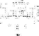
图1是示意性地示出EEPROM器件的剖视图。FIG. 1 is a cross-sectional view schematically showing an EEPROM device.
参考图1,在半导体衬底10中形成隔离区域之后,执行用于调整单元的阈值电压Vth的阱处理、光学处理(photo process)和离子注入处理。其后,在半导体衬底10上形成由氧化物层21、氮化物层23和氧化物层25构成的氧化物-氮化物-氧化物(ONO)层20。接下来,执行用于将ONO层20图案化的光学处理和蚀刻处理。随后,执行用于形成栅极氧化物层30的氧化处理。Referring to FIG. 1, after an isolation region is formed in a semiconductor substrate 10, a well process for adjusting a threshold voltage Vth of a cell, a photo process, and an ion implantation process are performed. Thereafter, an oxide-nitride-oxide (ONO) layer 20 composed of an oxide layer 21 , a nitride layer 23 and an oxide layer 25 is formed on the semiconductor substrate 10 . Next, optical processing and etching processing for patterning the ONO layer 20 are performed. Subsequently, oxidation treatment for forming gate oxide layer 30 is performed.
使用光学处理和蚀刻处理来形成和图案化栅极层,以形成第一栅极41和第二栅极42。接下来,执行用于形成结50,例如源/漏结51和中间转移节点结53的掺杂物离子注入处理。The gate layer is formed and patterned using optical processing and etching processing to form the first gate 41 and the second gate 42 . Next, a dopant ion implantation process for forming junctions 50 such as source/drain junction 51 and intermediate transfer node junction 53 is performed.
此后,形成介电层60和穿透介电层60的接触部分65,并且可以形成位线。Thereafter, the dielectric layer 60 and the contact portion 65 penetrating the dielectric layer 60 are formed, and a bit line may be formed.
但是,基于双晶体管的这种单元结构因为中间转移节点结53而伴随着单元面积的增加。即,作为存取栅极的第一栅极41和作为单元栅极的第二栅极42是在一个平面上分开放置的,从而因为这种平面结构而增加了单元面积。因此,难以用这种方法减少单元面积。However, such a cell structure based on two transistors is accompanied by an increase in cell area because of the intermediate transfer node junction 53 . That is, the first gate 41 as an access gate and the second gate 42 as a cell gate are separately placed on one plane, thereby increasing the cell area due to this planar structure. Therefore, it is difficult to reduce the cell area by this method.
发明内容Contents of the invention
为解决现有技术的上述问题,本发明通过实施例提供了一种半导体器件及其制造方法。In order to solve the above-mentioned problems in the prior art, the present invention provides a semiconductor device and a manufacturing method thereof through embodiments.
实施例涉及半导体器件,且更具体地说,涉及制造具有自对准硅-氧化物-氮化物-氧化物-硅(SONOS)结构的分裂栅极型闪速电可擦可编程只读存储器(EEPROM)器件。Embodiments relate to semiconductor devices, and more particularly, to fabricating a split-gate flash EEPROM having a self-aligned silicon-oxide-nitride-oxide-silicon (SONOS) structure ( EEPROM) devices.
实施例涉及制造能减少单元面积的EEPROM器件的方法。Embodiments relate to methods of fabricating EEPROM devices capable of reducing cell area.
根据实施例,提供了一种方法,包括:在半导体衬底上形成掩模图案;在通过掩模图案暴露出来的半导体衬底的顶部上形成栅极氧化物层;在栅极氧化物层的顶部上形成与掩模图案的两侧壁都自对准的存取栅极;除去掩模图案;形成被附接到存取栅极的侧壁的第一电介质间隔件;形成适合覆盖存取栅极和第一电介质间隔件的绝缘层;以及形成两个单元栅极,分别与两个存取栅极的相对侧壁自对准,每个第一电介质间隔件被插入到相应的单元栅极与相应的存取栅极之间,单元栅极是在绝缘层的顶部上分开设置的。According to an embodiment, there is provided a method including: forming a mask pattern on a semiconductor substrate; forming a gate oxide layer on top of the semiconductor substrate exposed through the mask pattern; forming an access gate self-aligned with both sidewalls of the mask pattern on top; removing the mask pattern; forming a first dielectric spacer attached to the sidewalls of the access gate; an insulating layer of the gate and the first dielectric spacer; and forming two cell gates, respectively self-aligned with the opposite sidewalls of the two access gates, each first dielectric spacer being inserted into a corresponding cell gate Between the electrodes and the corresponding access gates, the cell gates are spaced apart on top of the insulating layer.
该方法还包括,在形成两个单元栅极之后,利用单元栅极作为蚀刻掩模,选择性地去除绝缘层的暴露部分。The method also includes, after forming the two cell gates, selectively removing exposed portions of the insulating layer using the cell gates as an etching mask.
该方法还包括,在选择性地去除绝缘层的暴露部分之后,通过离子注入,在半导体衬底的通过存取栅极和单元栅极暴露的部分上形成源极结和漏极结以及中间转移节点结。The method further includes, after selectively removing exposed portions of the insulating layer, forming source and drain junctions and intermediate transitions on portions of the semiconductor substrate exposed by the access gates and the cell gates by ion implantation. node knot.
可将掩模图案形成为包含两个不同的介电层。The mask pattern can be formed to include two different dielectric layers.
形成存取栅极还可包括:形成存取栅极层以覆盖掩模图案;在存取栅极层的顶部上形成第二间隔件层;以及回蚀第二间隔件层和存取栅极层。Forming the access gate may further include: forming an access gate layer to cover the mask pattern; forming a second spacer layer on top of the access gate layer; and etching back the second spacer layer and the access gate layer.
形成单元栅极可包括:形成单元栅极层;在单元栅极层的顶部上形成第三间隔件层;以及回蚀第三间隔件层和单元栅极层。Forming the cell gate may include: forming a cell gate layer; forming a third spacer layer on top of the cell gate layer; and etching back the third spacer layer and the cell gate layer.
绝缘层可以是氧化物-氮化物-氧化物(ONO)层。The insulating layer may be an oxide-nitride-oxide (ONO) layer.
因此,实施例示出了能够减少单元面积的制造EEPROM器件的方法。Thus, the embodiments illustrate a method of fabricating an EEPROM device capable of reducing cell area.
附图说明Description of drawings
图1是示意性示出制造EEPROM器件的方法的剖面图;以及1 is a cross-sectional view schematically illustrating a method of manufacturing an EEPROM device; and
示例性的图2到图8是示意性示出根据实施例的EEPROM器件的剖面图。Example FIGS. 2 to 8 are cross-sectional views schematically illustrating an EEPROM device according to an embodiment.
具体实施方式Detailed ways
参考图2,制备半导体衬底100,并形成浅沟槽隔离(STI)区域。此后,执行用于调整单元的阈值电压Vth的阱处理和光学处理以及离子注入处理。Referring to FIG. 2, a
参考图3,形成自对准栅极所需的掩模图案200。更具体地说,通过顺序沉积由不同绝缘材料制成的第一和第二介电层来形成第一掩模层210和第二掩模层230。此后,通过光刻处理来图案化掩模层以形成掩模图案200。Referring to FIG. 3, a mask pattern 200 required for a self-aligned gate is formed. More specifically, the first mask layer 210 and the second mask layer 230 are formed by sequentially depositing first and second dielectric layers made of different insulating materials. Thereafter, the mask layer is patterned through a photolithography process to form a mask pattern 200 .
参考图4,在半导体衬底100的暴露在掩模图案200两侧上的部分上生长硅氧化物层以形成栅极氧化物层300。此后,将用于第一栅极410(为存取栅极)的层,例如导体多晶硅层,沉积在每个栅极氧化物层300的顶部上,并在用于第一栅极410的层的顶部上形成第一间隔件层。Referring to FIG. 4 , a silicon oxide layer is grown on a portion of the
接下来,执行间隔件蚀刻,例如各向异性干法蚀刻,来形成第一间隔件250。通过各向异性干法蚀刻,利用第一间隔件250作为蚀刻掩模,来蚀刻亦即回蚀用于第一栅极410的暴露的层,以形成第一栅极410,第一栅极410为存取栅极。第一栅极410的线宽是由第一间隔件250的沉积厚度(或者线宽:临界尺寸[CD])来确定的。Next, spacer etching, such as anisotropic dry etching, is performed to form the
由于第一栅极410被形成为与掩模图案200和第一间隔件250自对准,所以第一栅极410的长度和临界尺寸是由第一间隔件250的临界尺寸和用于第一栅极410的层的沉积厚度来控制的。因此,可以通过精密地控制第一间隔件250和第一栅极410等的沉积厚度来巧妙地控制第一栅极410的临界尺寸。因此,可以获得第一栅极410的非常窄的临界尺寸。Since the
参考图5,选择性地去除掩模图案200。此后,通过用于沉积第二电介质间隔件层的处理并且回蚀第二间隔件层,形成被附接到第一栅极410的侧壁的第二电介质间隔件270。接下来,如图6所示,在半导体衬底100的通过第二间隔件270和第一栅极410暴露的部分上,形成由氧化物层510、氮化物层530和氧化物层550构成的ONO层500。Referring to FIG. 5, the mask pattern 200 is selectively removed. Thereafter, through a process for depositing a second dielectric spacer layer and etching back the second spacer layer, the second
此后,将用于第二栅极450(其为单元栅极)的层,例如导电多晶硅层,沉积在ONO层500的顶部上。在掩模图案200的两个侧壁上分开形成第二栅极450,第二栅极450是分开设置在两个第一栅极410之间的单元栅极,这样是为了打开两个栅极450之间的中间区域。Thereafter, a layer for the second gate 450 (which is the cell gate), such as a conductive polysilicon layer, is deposited on top of the
更具体地说,在沉积用于第二栅极450的层之后,在用于第二栅极450的层的顶部上形成第三间隔件层。接下来,执行包括间隔件蚀刻的回蚀处理,例如各向异性干法蚀刻,以形成第三间隔件290。这种用于形成第三间隔件290的处理可以省略。More specifically, after depositing the layer for the
通过各向异性干法蚀刻,利用第三间隔件290作为蚀刻掩模来蚀刻亦即回蚀用于第二栅极450的暴露的层,以形成第二栅极450,第二栅极450为单元栅极。第二栅极450的临界尺寸是由第三间隔件290的衬底厚度(或者临界尺寸[CD])来确定的。By anisotropic dry etching, using the
由于第二栅极450被形成为与第一栅极410和第三间隔件290自对准,所以第二栅极450的长度和临界尺寸是由第三间隔件290的临界尺寸(或者沉积厚度)或者用于第二栅极450的层的沉积厚度来控制的。因此,可以通过精密地控制第三间隔件290和用于第二栅极450的层的沉积厚度来巧妙地控制第二栅极450的临界尺寸。因此,可以获得第二栅极450的非常窄的临界尺寸。Since the
在上面的处理中,可以省略第三间隔件290。In the above process, the
参考图7,回蚀通过第三间隔件290和第一栅极410和第二栅极450暴露出来的下面的ONO层500,以暴露半导体衬底100的下面部分。Referring to FIG. 7 , the underlying
参考图8,在执行再氧化处理之后,通过离子注入处理形成结600,例如源/漏极结610和中间转移节点结630。在层间电介质700形成之后,形成穿过层间电介质700的接触部分750,以及连接到接触部分750的线800,例如位线。Referring to FIG. 8, after the re-oxidation process is performed,
如上所述,第一栅极410,其为存取栅极410,能够以自对准的方式被图案化,从而保证对长度和临界尺寸的稳定控制。由于可以通过控制第二间隔件270的厚度来适当地调整中间转移节点结630的宽度,所以能够防止在单元操作中可能发生的性能降低。As described above, the
如上所述,形成了自对准存取栅极和单元栅极,因此单元面积可以被最小化,同时防止了过度擦写的发生。因此,因使用SONOS单元而导致的对单元尺寸的限制可以被消除,使得SONOS单元可以应用于各种产品。As described above, self-aligned access gates and cell gates are formed so that the cell area can be minimized while preventing excessive erasure from occurring. Therefore, the limitation on the size of the unit resulting from the use of the SONOS unit can be eliminated, so that the SONOS unit can be applied to various products.
本领域技术人员应该清楚,在所公开的实施例中可以做出各种修改和变化。因此,所公开的实施例旨在覆盖明显和清楚的修改和变化,只要它们落在所属权利要求将其等价物的范围内。It will be apparent to those skilled in the art that various modifications and changes can be made in the disclosed embodiments. Thus, the disclosed embodiments are intended to cover obvious and obvious modifications and changes provided they come within the scope of equivalents of the appended claims.
Claims (8)
Translated fromChineseApplications Claiming Priority (2)
| Application Number | Priority Date | Filing Date | Title |
|---|---|---|---|
| KR1020050129654AKR100661225B1 (en) | 2005-12-26 | 2005-12-26 | Ipyrom device manufacturing method |
| KR1020050129654 | 2005-12-26 |
Publications (2)
| Publication Number | Publication Date |
|---|---|
| CN1992232Atrue CN1992232A (en) | 2007-07-04 |
| CN100552923C CN100552923C (en) | 2009-10-21 |
Family
ID=37815519
Family Applications (1)
| Application Number | Title | Priority Date | Filing Date |
|---|---|---|---|
| CNB200610170170XAExpired - Fee RelatedCN100552923C (en) | 2005-12-26 | 2006-12-25 | Method of Manufacturing EEPROM Devices |
Country Status (3)
| Country | Link |
|---|---|
| US (1) | US7396723B2 (en) |
| KR (1) | KR100661225B1 (en) |
| CN (1) | CN100552923C (en) |
Cited By (5)
| Publication number | Priority date | Publication date | Assignee | Title |
|---|---|---|---|---|
| CN102412207A (en)* | 2010-09-23 | 2012-04-11 | 新加坡商格罗方德半导体私人有限公司 | Eeprom cell |
| US8470669B2 (en) | 2009-12-04 | 2013-06-25 | Semiconductor Manufacturing International (Shanghai) Corporation | System and method for EEPROM architecture |
| CN103855163A (en)* | 2012-12-05 | 2014-06-11 | 上海华虹宏力半导体制造有限公司 | Two-bit SONOS flash memory and manufacturing method thereof |
| CN103855161A (en)* | 2012-12-05 | 2014-06-11 | 上海华虹宏力半导体制造有限公司 | SONOS flash memory and manufacturing method thereof |
| CN106663698A (en)* | 2014-08-04 | 2017-05-10 | 赛普拉斯半导体公司 | Split-gate semiconductor device with l-shaped gate |
Families Citing this family (5)
| Publication number | Priority date | Publication date | Assignee | Title |
|---|---|---|---|---|
| KR101038873B1 (en) | 2008-11-06 | 2011-06-02 | 주식회사 동부하이텍 | Manufacturing Method of Flash Memory Device |
| JP5985293B2 (en)* | 2011-10-04 | 2016-09-06 | ルネサスエレクトロニクス株式会社 | Semiconductor device and manufacturing method of semiconductor device |
| JP5684414B2 (en)* | 2014-01-24 | 2015-03-11 | ルネサスエレクトロニクス株式会社 | Manufacturing method of semiconductor device |
| JP6385873B2 (en)* | 2015-03-30 | 2018-09-05 | ルネサスエレクトロニクス株式会社 | Semiconductor device and manufacturing method thereof |
| CN108878439A (en)* | 2018-06-29 | 2018-11-23 | 上海华虹宏力半导体制造有限公司 | SONOS non-volatility memorizer and its manufacturing method |
Family Cites Families (5)
| Publication number | Priority date | Publication date | Assignee | Title |
|---|---|---|---|---|
| JP3512959B2 (en)* | 1996-11-14 | 2004-03-31 | 株式会社東芝 | Semiconductor device and manufacturing method thereof |
| KR20000027282A (en)* | 1998-10-27 | 2000-05-15 | 김영환 | Method for manufacturing split-gate type flash memory cell |
| US6359305B1 (en)* | 1999-12-22 | 2002-03-19 | Turbo Ic, Inc. | Trench-isolated EEPROM flash in segmented bit line page architecture |
| WO2003015172A2 (en) | 2001-08-06 | 2003-02-20 | Koninklijke Philips Electronics N.V. | Method of manufacturing a non-volatile memory |
| KR100546379B1 (en)* | 2003-09-15 | 2006-01-26 | 삼성전자주식회사 | Local Sonos Type Nonvolatile Memory Device Using Self-Alignment Method and Manufacturing Method Thereof |
- 2005
- 2005-12-26KRKR1020050129654Apatent/KR100661225B1/ennot_activeExpired - Fee Related
- 2006
- 2006-12-20USUS11/613,801patent/US7396723B2/enactiveActive
- 2006-12-25CNCNB200610170170XApatent/CN100552923C/ennot_activeExpired - Fee Related
Cited By (9)
| Publication number | Priority date | Publication date | Assignee | Title |
|---|---|---|---|---|
| US8470669B2 (en) | 2009-12-04 | 2013-06-25 | Semiconductor Manufacturing International (Shanghai) Corporation | System and method for EEPROM architecture |
| CN102412207A (en)* | 2010-09-23 | 2012-04-11 | 新加坡商格罗方德半导体私人有限公司 | Eeprom cell |
| CN102412207B (en)* | 2010-09-23 | 2014-05-07 | 新加坡商格罗方德半导体私人有限公司 | Eeprom cell |
| CN103855163A (en)* | 2012-12-05 | 2014-06-11 | 上海华虹宏力半导体制造有限公司 | Two-bit SONOS flash memory and manufacturing method thereof |
| CN103855161A (en)* | 2012-12-05 | 2014-06-11 | 上海华虹宏力半导体制造有限公司 | SONOS flash memory and manufacturing method thereof |
| CN103855161B (en)* | 2012-12-05 | 2016-06-08 | 上海华虹宏力半导体制造有限公司 | A kind of SONOS flash memories and manufacture method thereof |
| CN103855163B (en)* | 2012-12-05 | 2016-12-21 | 上海华虹宏力半导体制造有限公司 | Two bit SONOS flash memories and manufacture methods thereof |
| CN106663698A (en)* | 2014-08-04 | 2017-05-10 | 赛普拉斯半导体公司 | Split-gate semiconductor device with l-shaped gate |
| US10593688B2 (en) | 2014-08-04 | 2020-03-17 | Cypress Semiconductor Corporation | Split-gate semiconductor device with L-shaped gate |
Also Published As
| Publication number | Publication date |
|---|---|
| US7396723B2 (en) | 2008-07-08 |
| KR100661225B1 (en) | 2006-12-22 |
| CN100552923C (en) | 2009-10-21 |
| US20070148866A1 (en) | 2007-06-28 |
Similar Documents
| Publication | Publication Date | Title |
|---|---|---|
| CN1992232A (en) | Method of manufacturing eeprom device | |
| KR100546352B1 (en) | Flash memory having local SONOS structure using notched gate and manufacturing method thereof | |
| US7652322B2 (en) | Split gate flash memory device having self-aligned control gate and method of manufacturing the same | |
| KR0136995B1 (en) | Manufacturing method of nonvolatile memory cell | |
| US7316945B2 (en) | Method of fabricating a fin field effect transistor in a semiconductor device | |
| CN1868069A (en) | Recess channel flash architecture for reduced short channel effect | |
| US8629025B2 (en) | Semiconductor device and method for fabricating semiconductor device | |
| KR20060084444A (en) | 2-transistor memory cell and fabrication method | |
| CN1235377A (en) | Semiconductor memory device and method of manufacturing the same | |
| CN1290191C (en) | Integrated circuit device and its mfg. method | |
| CN1855447A (en) | Method for manufacturing flash memory device | |
| US7172938B2 (en) | Method of manufacturing a semiconductor memory device | |
| KR100608369B1 (en) | Manufacturing method of MOSFET device in the peripheral area | |
| CN1694242A (en) | Method of manufacturing flash memory device | |
| CN1181535C (en) | Manufacturing method of embedded non-volatile semiconductor memory cell | |
| CN1992182A (en) | Method of manufacturing a transistor of a semiconductor device | |
| CN100505219C (en) | Method of manufacturing non-volatile memory device and memory device obtained therefrom | |
| KR100561970B1 (en) | Manufacturing method of semiconductor device | |
| KR100742758B1 (en) | Flash memory device and manufacturing method thereof | |
| CN1224080C (en) | Manufacturing method of floating gate in flash memory | |
| KR100652349B1 (en) | Self-aligned Sonos memory cell manufacturing method | |
| KR100562742B1 (en) | Semiconductor device and manufacturing method | |
| KR100422347B1 (en) | Method for fabricating flash memory device | |
| CN1349250A (en) | Method of forming gate by damascene process | |
| KR100989738B1 (en) | Flash memory having a spiral channel and a method of manufacturing the same |
Legal Events
| Date | Code | Title | Description |
|---|---|---|---|
| C06 | Publication | ||
| PB01 | Publication | ||
| C10 | Entry into substantive examination | ||
| SE01 | Entry into force of request for substantive examination | ||
| C14 | Grant of patent or utility model | ||
| GR01 | Patent grant | ||
| C17 | Cessation of patent right | ||
| CF01 | Termination of patent right due to non-payment of annual fee | Granted publication date:20091021 Termination date:20131225 |