CN1985439B - Headswitch and footswitch circuits for power management - Google Patents
Headswitch and footswitch circuits for power managementDownload PDFInfo
- Publication number
- CN1985439B CN1985439BCN2005800235523ACN200580023552ACN1985439BCN 1985439 BCN1985439 BCN 1985439BCN 2005800235523 ACN2005800235523 ACN 2005800235523ACN 200580023552 ACN200580023552 ACN 200580023552ACN 1985439 BCN1985439 BCN 1985439B
- Authority
- CN
- China
- Prior art keywords
- logic
- cells
- switch
- power
- integrated circuit
- Prior art date
- Legal status (The legal status is an assumption and is not a legal conclusion. Google has not performed a legal analysis and makes no representation as to the accuracy of the status listed.)
- Expired - Lifetime
Links
Images


Classifications
- H—ELECTRICITY
- H03—ELECTRONIC CIRCUITRY
- H03K—PULSE TECHNIQUE
- H03K19/00—Logic circuits, i.e. having at least two inputs acting on one output; Inverting circuits
- H03K19/0008—Arrangements for reducing power consumption
- H03K19/0016—Arrangements for reducing power consumption by using a control or a clock signal, e.g. in order to apply power supply
Landscapes
- Physics & Mathematics (AREA)
- Engineering & Computer Science (AREA)
- Computer Hardware Design (AREA)
- Computing Systems (AREA)
- General Engineering & Computer Science (AREA)
- Mathematical Physics (AREA)
- Semiconductor Integrated Circuits (AREA)
- Switch Cases, Indication, And Locking (AREA)
Abstract
Description
Translated fromChinese技术领域technical field
本发明涉及集成电路,且更具体而言涉及用于集成电路的电源管理的头部开关及脚部开关。The present invention relates to integrated circuits, and more particularly to headswitches and footswitches for power management of integrated circuits.
背景技术Background technique
包含集成电路(例如应用专用集成电路(ASIC))的电子装置常常采用节电技术来减少功率消耗且进而获得延长的电池寿命。例如,小型便携式装置(例如移动电话及个人数字助理(PDA))通常包含用于执行非现用模式的电路来限制逻辑电路的功率消耗。非现用模式可包括备用模式、低功率模式及睡眠模式。Electronic devices that include integrated circuits, such as application specific integrated circuits (ASICs), often employ power saving techniques to reduce power consumption and thereby achieve extended battery life. For example, small portable devices such as mobile phones and personal digital assistants (PDAs) often include circuitry for performing an inactive mode to limit the power consumption of logic circuits. Inactive modes may include standby mode, low power mode, and sleep mode.
数字电路中且更具体而言CMOS电路中的功率消耗近似与供电电压的平方成正比。因此,实现低功率性能的最有效方法是按比例减小供电电压。ASIC上的CMOS电路能够以显著减小的功率水平工作。然而,为了避免传播延迟的增加,还减小CMOS装置的阈值电压。Power consumption in digital circuits, and more specifically in CMOS circuits, is approximately proportional to the square of the supply voltage. Therefore, the most effective way to achieve low power performance is to scale down the supply voltage. CMOS circuits on ASICs are able to operate at significantly reduced power levels. However, to avoid an increase in propagation delay, the threshold voltage of the CMOS device is also reduced.
由于MOS装置的亚阈值泄漏电流的变化,阈值电压的减小通常会导致备用电流的增加。流过一“关断”的晶体管的泄漏电流往往会随一装置的阈值电压的减小而以指数方式增加。因此,长时期地保持处于非现用模式的电子装置(例如移动电话及PDA)可表现出显著的泄漏电流,并在所述非现用模式期间造成不期望有的电池电力耗用。A decrease in threshold voltage typically results in an increase in standby current due to variations in the subthreshold leakage current of the MOS device. The leakage current flowing through an "off" transistor tends to increase exponentially as the threshold voltage of a device decreases. Accordingly, electronic devices such as mobile phones and PDAs that remain in inactive mode for extended periods of time can exhibit significant leakage current and cause undesirable battery power drain during the inactive mode.
为了减小在备用模式期间的泄漏电流,一些ASIC包括电连接于一CMOS电路的低电压阈值(LVT)逻辑门与电源轨条或接地轨条之间的头部开关或脚部开关。头部开关为一高电压阈值(HVT)PMOS晶体管,其位于一ASIC核心或块的本地电源网格布线与顶层电源网格布线之间。脚部开关为一位于本地接地网格布线与顶层接地轨条/网格之间的HVT NMOS晶体管。To reduce leakage current during standby mode, some ASICs include headswitches or footswitches electrically connected between a low voltage threshold (LVT) logic gate of a CMOS circuit and a power or ground rail. The headswitch is a high voltage threshold (HVT) PMOS transistor located between the local and top-level power rail routing of an ASIC core or block. The footswitch is a HVT NMOS transistor located between the local ground grid routing and the top ground rail/hatch.
在一非现用模式期间,所述头部开关或脚部开关关断以将所述LVT逻辑门从所述电源/地电源断开且从而使所述电源轨条“崩溃”。由于所述头部开关或脚部开关具有一高的阈值电压,因此所述头部开关或脚部开关从所述电源中吸收的泄漏电流量相对于原本流过所述LVT逻辑门的泄漏电流明显减少。在一现用模式期间,所述头部开关或脚部开关接通以将所述电源及接地连接至所述LVT门。因此,在一现用模式期间,所述LVT逻辑门由与假如其直接连接至所述电源及接地时基本相同的电压供电。During an inactive mode, the headswitch or footswitch is turned off to disconnect the LVT logic gate from the power/ground supply and thereby "crash" the power rail. Since the headswitch or footswitch has a high threshold voltage, the amount of leakage current that the headswitch or footswitch draws from the power supply is relatively small relative to the leakage current that would otherwise flow through the LVT logic gate. obviously decrease. During an active mode, the headswitch or footswitch is on to connect the power and ground to the LVT gate. Thus, during an active mode, the LVT logic gate is powered by substantially the same voltage as if it were connected directly to the power supply and ground.
令人遗憾的是,在全局基础上构建头部开关或脚部开关电路以使一大逻辑单元阵列的电源轨条崩溃可能非常复杂。现有的方法已依靠专用的布线及定制分析及设计工具。很多问题使现有头部开关及脚部开关构建方案的复杂度进一步增大,所述问题包括用于为所述头部开关及脚部开关馈电的额外电源布线、显著的面积开销、难以处理的IR压降、信号布线容纳、标准工具流程及方法的复杂性及馈通的使用。Unfortunately, building a headswitch or footswitch circuit on a global basis to collapse the power rails of a large array of logic cells can be very complex. Existing approaches have relied on dedicated routing and custom analysis and design tools. A number of issues further complicate existing headswitch and footswitch implementations, including additional power wiring to feed the headswitch and footswitches, significant area overhead, difficult Dealing with IR drop, signal routing accommodation, complexity of standard tool flows and methodologies, and use of feedthrough.
发明内容Contents of the invention
大体而言,本发明涉及用于在例如ASIC等集成电路中构建用于电源管理的头部开关及脚部开关的电路。所揭示电路不仅支持有效的电源管理,而且支持集成电路面积的有效使用、降低的复杂度及电子设计自动化(EDA)工具的使用。通过此种方式,所揭示电路可支持增强的性能及简化的ASIC设计。In general, the present invention relates to circuits for building headswitches and footswitches for power management in integrated circuits such as ASICs. The disclosed circuits not only support efficient power management, but also efficient use of integrated circuit area, reduced complexity, and use of electronic design automation (EDA) tools. In this way, the disclosed circuits can support enhanced performance and simplified ASIC design.
在一些实施例中,头部开关或脚部开关电路可构建成一围绕一形成一ASIC核心的一部分的硬宏延伸的开关焊盘环。在其他实施例中,可通过将头部开关或脚部开关组件嵌入耦接至标准逻辑单元行的金属2(M2)层电源布线下面来使头部开关或脚部开关分布于一ASIC核心内。In some embodiments, the headswitch or footswitch circuitry may be implemented as a ring of switch pads extending around a hard macro forming part of an ASIC core. In other embodiments, headswitches or footswitches may be distributed within an ASIC core by embedding the headswitch or footswitch assembly under metal 2 (M2) layer power routing coupled to standard logic cell rows .
本发明中所述的电路可适用于各种电子装置,但可尤其适用于依靠非现用电路模式来节约电池电力的小型便携式无线通信装置。The circuits described in this disclosure are applicable to a variety of electronic devices, but may be especially applicable to small portable wireless communication devices that rely on inactive circuit modes to conserve battery power.
在一实施例中,本发明涉及一种集成电路,其包括一包含复数个逻辑单元的逻辑电路及一布置于所述逻辑电路周围的焊盘环。一外部端子提供一第一供电电位,且一内部端子提供一第二供电电位。所述焊盘环内的复数个开关单元中的每一个均将所述外部端子电耦接至所述内部端子,以有选择地将所述第二供电电位施加至所述逻辑电路内的所述逻辑单元。所述开关单元可包括头部开关或脚部开关。另外,可在所述逻辑电路中提供馈通单元以选择性地驱动所述开关单元。In one embodiment, the invention relates to an integrated circuit comprising a logic circuit including a plurality of logic cells and a pad ring arranged around the logic circuit. An external terminal provides a first power supply potential, and an internal terminal provides a second power supply potential. Each of the plurality of switching cells within the pad ring electrically couples the external terminal to the internal terminal for selectively applying the second supply potential to all of the logic circuits within the logic circuit. the logic unit. The switch unit may include a head switch or a foot switch. In addition, a feedthrough unit may be provided in the logic circuit to selectively drive the switching unit.
在另一实施例中,本发明涉及一种集成电路,所述集成电路包括:一包括复数个逻辑单元的逻辑电路,一设置于所述逻辑单元区域上的金属2层电源轨条,及一设置于所述逻辑单元区域上的金属2层接地轨条。所述金属2层下面的复数个开关单元中的每一个均选择性地耦接及解耦接所述电源轨条及所述接地轨条中的一者以为所述逻辑单元中的至少一些逻辑单元供电。所述开关单元可包括头部开关或脚部开关,且可由所述逻辑电路内的馈通单元驱动。In another embodiment, the present invention is directed to an integrated circuit comprising: a logic circuit including a plurality of logic cells, a metal 2-layer power rail disposed on the logic cell area, and a A metal layer 2 ground rail placed on the logic cell area. Each of the plurality of switching cells below the metal 2 layer selectively couples and decouples one of the power rail and the ground rail for at least some of the logic cells unit powered. The switch unit may comprise a head switch or a foot switch and may be driven by a feedthrough unit within the logic circuit.
在附图及下文说明中列出一个或多个实施例的细节。根据本说明及附图及根据权利要求书将易知其他特征、目的及优点。The details of one or more embodiments are set forth in the accompanying drawings and the description below. Other features, objects, and advantages will be apparent from the description and drawings, and from the claims.
附图说明Description of drawings
图1为一图解说明一具有一头部开关的多阈值CMOS(MTCMOS)电路的电路图。FIG. 1 is a circuit diagram illustrating a multi-threshold CMOS (MTCMOS) circuit with a headswitch.
图2为一图解说明一具有一脚部开关的多阈值CMOS(MTCMOS)电路的电路图。FIG. 2 is a circuit diagram illustrating a multi-threshold CMOS (MTCMOS) circuit with a foot switch.
图3为一图解说明一包括设置于一集成电路中一硬宏核心的周边周围的垂直式、水平式及拐角式头部开关或脚部开关的开关焊盘环的布局图。3 is a layout diagram illustrating a switch pad ring including vertical, horizontal and corner headswitches or footswitches disposed around the perimeter of a hard macro core in an integrated circuit.
图4为一图解说明一可用于构建图3中开关焊盘环的垂直式、水平式及拐角式单元的实例性头部开关的电路图。4 is a circuit diagram illustrating an example headswitch that may be used to construct the vertical, horizontal, and corner cells of the switch pad ring of FIG. 3 .
图5为一图解说明一可用于构建图3中开关焊盘环的垂直式、水平式及拐角式单元的实例性脚部开关的电路图。5 is a circuit diagram illustrating an example footswitch that may be used to construct vertical, horizontal, and corner cells of the switch pad ring of FIG. 3. FIG.
图6为一图解说明使头部开关分布于一集成电路中金属2(M2)电源路径下面的布局图。6 is a layout diagram illustrating distribution of headswitches under metal 2 (M2) power paths in an integrated circuit.
图7为一更详细地说明图6所示头部开关的分布式图案的布局图。FIG. 7 is a layout diagram illustrating in more detail the distributed pattern of the headswitches shown in FIG. 6 .
图8为一图解说明一包含本发明中所述的逻辑电路的电子装置的方块图。FIG. 8 is a block diagram illustrating an electronic device including the logic circuits described in this disclosure.
图9为一图解说明一如图3所示的开关焊盘环的布局图,但所述水平式开关单元中的几个被去耦电容单元所代替。FIG. 9 is a layout diagram illustrating a switch pad ring as shown in FIG. 3 but with several of the horizontal switch cells replaced by decoupling capacitor cells.
具体实施方式Detailed ways
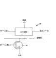
图1为一图解说明一具有一头部开关18的多阈值CMOS(MTCMOS)电路10的电路图。电路10形成一集成电路(例如一ASIC)中的一逻辑电路的一部分。电路10经配置以在具有降低的电源及阈值电压的逻辑门中减小泄漏电流量。因此,电路10可特别适用于例如ASIC等包含一大的低电压阈值(LVT)逻辑门阵列的电路。在图1所示的实例中,一LVT逻辑门12电耦接至一“虚拟”电压电源节点VDDV及一实际接地电位GND。一输入信号(IN)16驱动逻辑门12,然后逻辑门12产生一输出信号(OUT)18。FIG. 1 is a circuit diagram illustrating a multi-threshold CMOS (MTCMOS)
一头部开关18将“虚拟”电压电源节点VDDV电耦接至全局电压电源VDD。电压电源VDD是自一位于包含逻辑门12的电路外部的外部端子提供。同样地,接地GND由一外部接地端子提供。头部开关18为一高电压阈值(HVT)或超高电压阈值(UHVT)PMOS晶体管。一栅极输入端20有选择地将一睡眠信号(SL)施加至头部开关18,从而使所述头部开关接通/断开并将实际电压电源VDD节点电耦接至“虚拟”电压电源节点VDDV及自“虚拟”电压电源节点VDDV解耦接,由此将LVT逻辑门12置于现用及非现用模式中。MTCMOS电路10的实际电压电源VDD及实际接地GND可由一电池提供。例如,在一移动电话中,VDD及GND具有一介于0.5与2.0伏特之间的电压差。A
LVT逻辑门12可包括任何配置形式的任何类型的逻辑门。例如,逻辑门可包括单个CMOS反相器,或者也可包括任意数量及任意组合形式的低电压阈值AND、NAND、OR、NOR、XOR、或其他类型的静态/动态逻辑门或存储器。形成头部开关18的高电压阈值晶体管在一正常工作模式(即现用模式)期间有选择地将实际电压电源VDD减去所述头部开关晶体管两端的压降施加至虚拟电压电源轨条VDDV以为LVT逻辑门12供电。相反地,在一非现用模式期间,头部开关18将实际电压电源VDD自虚拟电压电源轨条VDDV解耦接,从而使所述电源轨条崩溃。因此,当将栅极输入端20处的SL信号解除确定(即SL 14为低)时,头部开关18的输出且因此VDDV上的电压大致等于VDD。
在一睡眠或备用模式期间,将栅极输入端20处的睡眠信号SL解除确定以使头部开关18关断。在一非现用模式中自VDD吸收的泄漏电流量因头部开关18具有一高阈值电压且没有电流流过LVT逻辑门12而得到减少。相反,假如在一非现用模式期间未使用头部开关18,则LVT逻辑门12将电连接于实际供电电压VDD与实际接地参考GND之间,并在非现用模式期间产生一不期望有的泄漏电流量。During a sleep or standby mode, the sleep signal SL at the
同样地,在一现用模式期间,在栅极输入端20处确定睡眠信号SL,从而使头部开关18接通并将电压电源VDD耦接至虚拟电压电源VDDV,由此为LVT逻辑门12供电以在一现用模式中正常工作。因此,在一现用模式期间,实例性MTCMOS电路10的LVT逻辑门12由与假如其直接连接至VDD及GND时基本相同的电压供电。因此,实例性MTCMOS电路10允许降低LVT逻辑门120的阈值电压、同时减少在非现用模式期间的泄漏电流量。Likewise, during an active mode, sleep signal SL is asserted at
图2为一图解说明一具有一脚部开关24的多阈值CMOS(MTCMOS)电路22的电路图。电路22与图1所示的电路10基本一致,但包含脚部开关24而不是头部开关18。如图2中所示,MTCMOS电路22的LVT逻辑门4电耦接至由一外部电源轨条提供的实际电压电源VDD。然而,LVT逻辑门4耦接至虚拟接地节点GNDV,而不是实际接地节点GND。脚部开关24包括一高电压阈值(VHT)晶体管,所述高电压阈值(VHT)晶体管根据LVT逻辑门12的工作模式(即根据所述逻辑门是处于现用还是非现用模式中)选择性地将虚拟接地节点GNDV连接至实际接地节点GND及自实际接地节点GND断开。FIG. 2 is a circuit diagram illustrating a multi-threshold CMOS (MTCMOS)
输入栅极26将一睡眠信号SL施加至脚部开关24,以接通及关断所述脚部开关且由此将实际接地GND耦接至及自虚拟接地GNDV解耦接。当脚部开关24接通且实际上“闭合”时,虚拟接地节点GNDV连接至实际接地节点GND的电位减去脚部开关24两端的压降。如同电路10(图1)中的头部开关18一样,脚部开关24在现用模式中容许LVT逻辑门12由与假如其直接连接至实际接地GND时基本相同的电压来供电,但在非现用模式中不允许电流流过所述LVT逻辑门,从而减少泄漏电流。
虽然使用头部开关18或脚部开关24或以组合形式同时使用二者可有效地减少在例如ASIC等包含LVT逻辑电路的集成电路中的泄漏电流,但此方法可造成若干种复杂因素。具体而言,构建一头部开关或脚部开关以使所述电源轨条在一全局基础上(即对于一大的LVT逻辑门、单元或块阵列而言)崩溃可能非常复杂。例如,现有的头部开关及脚部开关构建方案通常依靠专用布线来有选择地将电压电源轨条或接地电位轨条耦接至各个LVT逻辑门。While the use of
现有的头部开关及脚部开关构建方案及相关联的布线复杂度可使布局复杂化且需要使用定制的电路分析及仿真工具。用于为所述头部开关及脚部开关馈电的额外电源布线、及由所述布线及所述头部开关/脚部开关电路造成的面积开销会进一步增加复杂度。在电路设计及布局中通常必须解决的其他问题包括其他IR压降、信号布线、标准工具流程及方法的复杂性、及馈通的使用。本发明阐述可设计用来缓解某些上述问题的头部开关及脚部开关构建方案。Existing headswitch and footswitch build schemes and the associated routing complexity can complicate layout and require the use of custom circuit analysis and simulation tools. Additional power supply wiring for feeding the headswitches and footswitches, and the area overhead caused by the wiring and the headswitch/footswitch circuitry further adds to the complexity. Other issues that typically must be addressed in circuit design and layout include additional IR drop, signal routing, complexity of standard tool flows and methods, and use of feedthrough. The present invention addresses headswitch and footswitch implementations that can be designed to alleviate some of the above-mentioned problems.
图3为一图解说明一包括设置于一集成电路(例如一ASIC)中一硬宏核心36的周边周围的垂直式、水平式及拐角式开关单元30、32、34的开关焊盘环28的布局图。开关焊盘环28以一种类似于一用于将一ASIC片(tile)中的打线接合焊盘耦接至IC封装引脚的传统焊盘环的方式设置于硬宏核心36周围。不过,在图3所示实例中,开关焊盘环28为集成电路内、尤其是具有低供电电压的电路中的LVT逻辑门提供全局电源管理。开关单元30、32、34可为头部开关或脚部开关。开关焊盘环28代表一全局头部开关或脚部开关电路的一替代构建方案。3 is a diagram illustrating a
开关焊盘环28的构建方案可提供简化的布局及布线,并且有利于利用在现有EDA系统中所提供的电路分析及仿真工具。另外,开关焊盘环28可促进更有效的面积利用及复杂度的降低。虽然为了易于说明起见图3描绘了一相对较小数量的开关单元30、32、34,但实际上可根据所述全局头部开关或脚部开关构建方案所应用于的ASIC核心的大小及密度而使用几百或几千个开关单元。The construction scheme of the
开关焊盘环28内的垂直式、水平式及拐角式开关单元30、32、34通过减少在非现用模式期间的泄漏电流量来有助于例如ASIC等集成电路的电源管理。具体而言,开关焊盘环28实际上在睡眠或备用模式期间在选择性基础上解耦接硬宏核心36内的LVT逻辑门,以避免泄漏电流流动。开关焊盘环28包括若干个经配置以容许一ASIC的一区域或块独立于所述ASIC的其他区域被供电及断电的不同开关单元30、32、34。Vertical, horizontal and
一ASIC可为一由电池操作的便携式电子装置的一部分。开关焊盘环28可尤其有利于便携式电子装置,例如移动电话、个人数字助理(PDA)或具有一其中ASIC的一部分继续工作而有些电路关断或处于一低功率状态中的睡眠或备用模式的其他此类装置。例如,开关焊盘环28可允许一移动电话的数字信号处理器(DSP)关断,同时ASIC的不同电路监控用于指示入局呼叫的接收信号的功率。An ASIC may be part of a battery operated portable electronic device. The
如图3中所示,开关焊盘环28包括沿所述焊盘环的一垂直范围定向的垂直式(V)开关单元30、沿所述焊盘环的一水平范围定向的水平式(H)开关单元32、及桥接垂直式与水平式开关单元之间的拐角空间的拐角式(C)开关单元34。在一些实施例中,间隔单元可定位于一些毗邻的开关焊盘环单元30、32、34之间。在实体上,且出于EDA目的,开关焊盘环单元30、32、34布置于一硬宏核心36周围。为了基于EDA设计的工具(例如VHDL、Verilog或类似工具)起见,硬宏核心36界定一由LVT逻辑门及相关联的电源及信号布线电路形成的硬化核心。As shown in FIG. 3 , the
每一开关单元30、32、34均包括一分别大致如图1及2中所示的头部开关或脚部开关,以在非现用模式期间将硬宏核心36内的电路自一呈外部电源环38形式的外部端子解耦接。外部电源环38自所述ASIC内的电源电路为实际电压电源(VDD)端子或“轨条”供电。虽然出于例示目的在本文中将对头部开关进行大体说明,但开关单元30、32、34可包括头部开关或脚部开关。Each
一呈内部电源环40形式的内部端子充当硬宏36内的组件的虚拟电压电源(VDDV)端子或“轨条”。因此,硬宏36由内部电源环40供电而外部电源环38自所述ASIC的一外部供电电压分接出。硬宏核心36中的LVT逻辑门可形成能够配装在更大功能块中的标准单元。例如,硬宏核心36可包括存储块、数字信号处理器(DSP)电路、定制的处理器核心、或任何其他硬化的知识产权(IP)核心。An internal terminal in the form of
当开关焊盘环28以具有三重井隔离(即一深N井)的头部开关或脚部开关构建而成时,用于构建硬宏36的标准单元可具有本地衬底连接线。然而,当开关焊盘环28以脚部开关构建而成时,用于构建硬宏36的标准单元可具有浮动的衬底连接线。When the
较佳地,对于位于ASIC设计体系的下一层次处的EDA布置及布线工具而言,开关焊盘环28可看上去为一形成硬宏核心36的一部分的标准单元,但带有一额外的开/关信号。硬宏核心36的引脚可在实体上布置在开关焊盘环28的外部但在所述硬宏的EDA边界的内部。因此,可在设计过程的顶部体系层次处简化时序收敛。另外,开关单元30、32、34的布置可完全自动化且开关焊盘环28可方便地平铺于硬宏核心36的周围。因此,即使包含头部开关或脚部开关,ASIC或其他集成电路的设计也会得到简化且设计者的工作负荷因由开关焊盘环28所提供的全局构建方案而减小。Preferably, to an EDA place and route tool at the next level of the ASIC design hierarchy, the
开关焊盘环28还通过利用根据需要可供用于去耦电容器的面积并使电源布线最少化来有效地利用面积。具体而言,金属2(M2)功率路径下面的面积可用于开关单元30、32、34或去耦电容器。在一些实施例中,如果所述ASIC的可适用的IR压降要求得不到满足,则有些开关单元30、32、34可由去耦电容器代替。例如,图9显示一开关焊盘环28′的一实施例,其中所述水平头部开关32中的一些被去耦电容单元DC所代替。另外,在使用头部开关来构建开关单元30、32、34的实施例中,开关焊盘环28内部不需要额外的布线。The
例如,可通过下述方式使用标准的VLSI设计工具及服务程序将开关焊盘环28平铺于硬宏核心36的周围:产生一初始连线表,插入馈通单元及头部开关并针对一ASIC或单芯片系统(SOC)的平面布局图正确地连接启用信号。设计者根据硬宏核心36的初始尺寸、电源及接地技术规范提供一包括用于垂直式、水平式及拐角式开关焊盘环单元的头部开关的数量的配置文件。另外,如上文所提及,如果IR压降分析表明插入了过多的头部开关,则可由解耦电容装置代替额外的头部开关。For example, the
图4为一图解说明一用于构建图3中所示开关焊盘环28的垂直式、水平式及拐角式开关焊盘环单元30、32、34的实例性头部开关42的电路图。头部开关42为一由栅极输入端44处的被确定为高的睡眠信号EN通过一馈通单元46控制的高电压阈值PMOS晶体管。来自外部电源环38(图3)的实际供电电压VDDX 48也电连接至头部开关42。FIG. 4 is a circuit diagram illustrating an example headswitch 42 for constructing the vertical, horizontal and corner switch
头部开关42的输出端VDD_INT 50电连接至内部电源环40(图3)。因此,VDD_INT 50用作硬宏36内的组件的虚拟电压电源。如图4中所示,馈通单元46电连接至VDDX 48及地电源VSSX 52。馈通单元46响应于栅极输入端44处的睡眠信号EN的状态为头部开关42提供足够的栅极-源极电压(Vgs)以接通及关断高阈值电压PMOS晶体管。馈通单元46也可经配置以使头部开关42的接通时间最佳化。The
头部开关42的尺寸通常受限于在外部电源环38跨所述头部开关连接至内部电源环40时的高电流负载期间头部开关42两端的最大压降。头部开关42较佳地用于垂直式、水平式及拐角式开关焊盘环单元30、32、34中的每一种中,虽然每一相应开关焊盘环单元的所述最大压降且因此尺寸可有所不同。例如,在一个特定实施例中,垂直式、水平式及拐角式开关单元30、32、34的各自的面积可分别约为252平方微米(42微米×6微米)、381平方微米(17.4×21.9微米)及919.8微米(42微米×21.9微米)。The size of the headswitch 42 is generally limited by the maximum voltage drop across the headswitch 42 during high current loading when the
硬宏36内的馈通单元46可具有一称作SVDDX的电源引脚,所述电源引脚电连接至外部电源环38。外部电源环38较宽地路由至所述SVDDX引脚。因此,电耦接至外部电源环38的引脚也较宽。此一馈通单元46还具有电连接至VDDX 32及VSSX38的引脚。然而,在馈通单元46内部,可仅使用SVDDX而不需要其他电源布线。
较佳地,馈通单元46可看上去为硬宏核心36内的一标准逻辑单元,但如上所述包括与外部电源环38的连接线。具体而言,馈通单元46可类似于其他标准逻辑单元,包括耦接至虚拟功率或接地端子的引脚,但进一步包括另外的一组耦接至外部电源及接地端子的引脚。即使馈通单元46包括虚拟电源及接地连接,从而看上去为一标准逻辑单元,但其实际上使用所述外部电源及接地连接线来工作。通过此种方式,馈通单元46可在其他逻辑单元关断且不接收外部电源的非现用模式期间工作,且从而可用于驱动开关焊盘环28内的头部开关或脚部开关。Preferably, the
在非现用模式期间,将栅极输入端44处的EN解除确定,以使头部开关42关断,且从而将VDDX 48自VDD_JNT 50解耦接。由于头部开关42具有一高阈值电压,因此硬宏核心36内的LVT逻辑门自VDDX 48所吸收的泄漏电流量减少。相反,假如在非现用模式期间不使用头部开关42,则硬宏核心36将电连接至VDDX 48及VSSX 52。During inactive mode, EN at
相反地,在现用模式期间,栅极输入端44处的信号EN得到确定以使头部开关42接通,以便将VDDX 48提供至VDD_INT 50且由此为硬宏36内的LVT逻辑门供电。因此,在现用模式期间,硬宏核心36由与假如硬宏核心36直接连接至VDDX 48及VSSX 52时基本相同的电压供电。因此,头部开关42允许硬宏36内的LVT逻辑门的阈值电压降低、同时减少在低功率模式期间的泄漏电流量。然而,同时,图3中所描绘的开关焊盘环构建方案会降低与诸多用于全局电源管理的现有头部开关及脚部开关构建方案相关联的复杂性。Conversely, during active mode, signal EN at
头部开关42两端的压降在所述头部开关接通时最小,且栅极输入端42处的EN信号随着时间斜升以便不显著影响自VDDX 48接出的其他电路。在初始通电时,所有头部开关42均可缺省地接通。然而,只有为热启动所需的头部开关将在电源复位(即热启动)后接通。在热启动后,软件可随后对寄存器进行编程以接通焊盘环28中的开关单元,从而建立必要的电源轨条并使所述开关焊盘环复位。The voltage drop across the headswitch 42 is minimal when the headswitch is on, and the EN signal at the gate input 42 is ramped up over time so as not to significantly affect other circuitry derived from
在一些实施例中,电路10(图1)可包括用于不同的硬宏核心的复数个焊盘环。在这些情况下,可根据需要单独使各个单独的开关焊盘环复位,以为不同的操作或应用加电。通过此种方式,可优化在电源崩溃后的加电开销。此外,每一焊盘环中开关单元的一缓冲网络均可设计成使其提供足以驱动大的头部开关的栅极的驱动电流、同时还优化所述头部开关的接通时间。In some embodiments, circuit 10 (FIG. 1) may include a plurality of pad rings for different hard macro cores. In these cases, individual switch pad rings can be individually reset as needed to power up a different operation or application. In this way, power-up overhead after a power crash can be optimized. Additionally, a snubber network of switch cells in each pad ring can be designed such that it provides sufficient drive current to drive the gates of large headswitches while also optimizing the turn-on time of the headswitches.
图5为一图解说明一可用于构建图3中所示开关焊盘环28的垂直式、水平式及拐角式开关焊盘环单元30、32、34的实例性脚部开关54的电路图。在图5所示的实例中,脚部开关54是一由被确定为低的睡眠信号EN 47通过馈通单元46控制的高电压阈值NMOS晶体管。来自外部电源环38(图3)的地电源VSSX 52电连接至脚部开关54,且脚部开关的漏极输出端VSS_INT 50电连接至内部电源环40(图3)。FIG. 5 is a circuit diagram illustrating an
馈通单元46提供一足以将脚部开关54偏置接通的栅极-源极电压(Vgs),并电连接至VDDX 48及地电源VSSX 52。图5所示的馈通单元46可另外优化脚部开关54的接通时间。类似于头部开关42,图5所示的脚部开关54用作垂直式、水平式及拐角式开关焊盘环单元30、32、34,且因此可具有约为参照图4所示实例所述的单元尺寸的不同单元尺寸。
当用于构建硬宏36的标准单元具有浮动的衬底连接线时,脚部开关54及硬宏核心36可共享同一衬底连接线。因此,硬宏核心36的P井衬底连接至VSSX 52。如果用于构建硬宏核心36的标准单元具有本地衬底连接线,则所述硬宏核心及脚部开关54可共享P井衬底的同一连接性。此种构建方案通常可能需要一额外的DN井层。如同在图4所示的实例中一样,馈通单元46可具有一电连接至外部电源环38的称作VDDX的电源引脚。When the standard cells used to build the
在低功率或备用模式期间,将信号EN 44解除确定以使脚部开关40关断并由此将硬宏36内的LVT逻辑门自接地VSSX 52断开。因脚部开关54具有一高阈值电压,自VDDX 48吸收的泄漏电流量从而得到减少。相反地,在现用模式期间,确定栅极输入端44处的信号EN以使脚部开关54接通并由此将VSS_INT 50(及VDDX 48)(二者)供给硬宏核心36。在此种情况下,在现用模式期间,硬宏核心36由与假如硬宏核心36直接连接于VDDX 48与VSSX 52之间时基本相同的电压供电。During low power or standby mode, signal
如同在图4所示实例中一样,图5中的EN 44随着时间斜升以便不显著影响可能正从与VDDX 48相同的电源分接出的其他硬宏。另外,图5所示的电路可设计成有利于在优化一电源崩溃之后在热启动中有效地加电。As in the example shown in FIG. 4,
图6为一图解说明一集成电路56的一部分的布局图,集成电路56的特点是将头部开关(HS)单元58A-58D(统称为58)分布于一位于所述电路中金属2(M2)电源路径60下面的条纹图案中。一般地,每一头部开关单元58均电耦接于电源路径60与一相应的标准单元行62A-62H(统称为62)之间。FIG. 6 is a layout diagram illustrating a portion of an integrated circuit 56 featuring head switch (HS) units 58A-58D (collectively 58) distributed over a metal 2 (M2 ) in the stripe pattern below the power path 60. Generally, each headswitch unit 58 is electrically coupled between the power path 60 and a corresponding standard cell row 62A- 62H (collectively referred to as 62 ).
在图3所示实例中,头部开关包含于一环绕一集成电路(例如ASIC)的硬宏的开关焊盘环中。然而,根据图6所示的替代构建方案,头部开关单元58分布于由集成电路56的硬宏核心所界定的各标准逻辑单元行62当中。具体而言,头部开关单元58嵌入为标准逻辑单元行62提供电源及接地布线的金属2层下面。In the example shown in FIG. 3, the headswitches are contained in a ring of switch pads surrounding a hard macro of an integrated circuit (eg, ASIC). However, according to an alternative implementation shown in FIG. 6 , the headswitch cells 58 are distributed among standard logic cell rows 62 defined by the hard macro core of the integrated circuit 56 . Specifically, the headswitch cell 58 is embedded under the Metal 2 layer that provides power and ground routing for the standard logic cell row 62 .
嵌入式头部开关单元58为集成电路56内的LVT逻辑门提供全局电源管理,同时实现面积的有效使用并有利于EDA工具的使用。每一头部开关单元58均将源极连接至电源路径60并将漏极连接至每一标准单元行62内各逻辑单元的本地电压端子。通过此种方式,头部开关单元58控制由电源路径60所提供的供电电压向各个逻辑单元的施加。Embedded headswitch unit 58 provides global power management for the LVT logic gates within integrated circuit 56 while enabling efficient use of area and facilitating the use of EDA tools. Each headswitch cell 58 has its source connected to power path 60 and its drain connected to the local voltage terminal of each logic cell within each standard cell row 62 . In this way, the headswitch unit 58 controls the application of the supply voltage provided by the power supply path 60 to the respective logic units.
图7为一更详细地图解说明图6所示头部开关58的分布式图案的布局图。如在图7中所示,集成电路56的金属2(M2)层包括:M2电源轨条64A、64B(统称为64),其在整个集成电路面积上分配一供电电压;及接地轨条66A、66B(统称为66),其在整个集成电路面积上分配一接地电位。不过,头部开关单元58A-58F位于全局电源轨条64与在标准单元行顶上具有本地电源轨条的标准单元行之间,以控制电源向各标准单元的分配。FIG. 7 is a layout diagram illustrating in more detail the distributed pattern of the headswitches 58 shown in FIG. 6 . As shown in FIG. 7, the metal 2 (M2) layer of integrated circuit 56 includes: M2 power rails 64A, 64B (collectively 64), which distribute a supply voltage across the integrated circuit area; and ground rail 66A. , 66B (collectively referred to as 66), which distributes a ground potential over the entire integrated circuit area. Headswitch cells 58A-58F, however, are located between global power rail 64 and standard cell rows with local power rails on top of the standard cell row to control the distribution of power to each standard cell.
每一头部开关58均通过一相应的电压条带70A-70C(统称为70)及接地条带72A-72C(统称为72)为一行或多行60标准单元68A-68F(统称为68)供电。头部开关58A通过一共用电压条带70A耦接至一第一行60A逻辑单元68及一第二行60B单元68,所述共用电压条带70A为这两行提供供电电压。一接地条带72A耦接至第一行60A中的单元68,而一接地条带72B耦接至第二行60B中的单元。Each headswitch 58 is organized into one or more rows 60 of standard cells 68A-68F (collectively 68) via a corresponding voltage strip 70A-70C (collectively 70) and ground strips 72A-72C (collectively 72) powered by. Headswitch 58A is coupled to a first row 60A of logic cells 68 and a second row 60B of cells 68 through a common voltage strip 70A that provides the supply voltage for both rows. A ground strap 72A is coupled to cells 68 in the first row 60A, and a ground strap 72B is coupled to cells in the second row 60B.
在图7所示实例中,接地条带72A、72B及72C电连接至M2接地轨条66A及66B,以从而在ASIC 56内的各单元68当中分配接地电位。然而,电压条带70A、70B、70C不直接耦接至M2电源轨条64A、64B。而是,头部开关58A、58B及58C分别将电压条带70A、70B、70C连接至M2电源轨条64A。头部开关58D、58E及58F分别将电压条带70A、70B、70C连接至M2电源轨条64B。In the example shown in FIG. 7 , ground straps 72A, 72B, and 72C are electrically connected to M2 ground rails 66A and 66B to thereby distribute ground potential among cells 68 within ASIC 56 . However, the voltage strips 70A, 70B, 70C are not directly coupled to the M2 power rails 64A, 64B. Instead, headswitches 58A, 58B, and 58C connect voltage strips 70A, 70B, 70C, respectively, to M2 power rail 64A. Headswitches 58D, 58E, and 58F connect voltage strips 70A, 70B, 70C, respectively, to M2 power rail 64B.
头部开关58A响应于一启用信号而打开及闭合,以有选择地将来自M2电源轨条64A的供电电压连接至行68A及68B中的各标准单元68及将所述供电电压自行68A及68B中的各标准单元68切断。通过此种方式,通过减少从由M2电源轨条64所提供的供电电压吸收的泄漏电流量,头部开关58有助于对集成电路56的核心区域进行电源管理。Headswitch 58A opens and closes in response to an enable signal to selectively connect the supply voltage from M2 power rail 64A to and from each standard cell 68 in rows 68A and 68B. Each standard cell 68 in is cut off. In this way, headswitch 58 facilitates power management of core areas of integrated circuit 56 by reducing the amount of leakage current drawn from the supply voltage provided by M2 power rail 64 .
使头部开关58分布于M2电源轨条64下面可尤其有利于具有一其中ASIC 56的一部分必须在所述ASIC内的其他电路关断或处于低功率状态下的同时继续工作的非现用模式的电子装置。具体而言,可对分布式头部开关58单独加以控制,以将供电电压自ASIC 56中的选定区域、块或行解耦接。一实例为移动电话,在移动电话中,在呼叫探测电路保持现用的同时使DSP功能变为非现用。Distributing the headswitch 58 below the M2 power rail 64 can be especially beneficial to have an inactive mode where a portion of the ASIC 56 must continue to operate while other circuits within the ASIC are powered down or in a low power state of electronic devices. In particular, distributed headswitches 58 may be individually controlled to decouple supply voltages from selected regions, blocks or rows within ASIC 56. An example is a mobile phone where the DSP function is made inactive while the call detection circuit remains active.
随着制造技术向更高集成度演进及最小可制造形体变得越来越小(例如90纳米、65纳米或45纳米及更低),从而进入纳米技术层次,对自觉式本地电源管理块的需要应变得更为重要。栅极泄漏及亚阈值泄漏将变得足够显著,以致于将需要与电源感测控制块相结合的分布式头部开关/脚部开关块来支持不同标准单元区域与全局电源网格的本地自觉睡眠模式状态隔离。As manufacturing technology evolves to higher levels of integration and the smallest manufacturable features become smaller (e.g. 90nm, 65nm or 45nm and below), entering the nanotechnology level, the need for conscious local power management blocks needs should become more important. Gate leakage and sub-threshold leakage will become significant enough that a distributed headswitch/footswitch block combined with a power sensing control block will be required to support local awareness of different standard cell regions and the global power grid Sleep mode state isolation.
在一些实施例中,可使用脚部开关来代替头部开关58或与头部开关58结合使用而几乎不或根本不影响集成电路56内的核心区域。在这些实施例中,脚部开关分布于M2接地路径55的下面,并连接至接地条带72。图7中所示的分布于电源轨条64及接地轨条66下面的头部开关及脚部开关可在结构上类似于图4及5中所描绘的那些头部开关及脚部开关。In some embodiments, a foot switch may be used in place of or in combination with head switch 58 with little or no impact on core areas within integrated circuit 56 . In these embodiments, the footswitches are distributed under the M2 ground path 55 and connected to the ground strap 72 . The headswitches and footswitches shown in FIG. 7 distributed under power rail 64 and ground rail 66 may be similar in structure to those depicted in FIGS. 4 and 5 .
本文中所述的头部开关或脚部开关构建方案可与例如ASIC或ASIC的功能组件等集成电路一起使用。所述ASIC可驻留于一由电池操作的便携式电子装置(例如一移动电话、PDA或其他此类装置)内或针对所述由电池操作的便携式电子装置加以配置。可提供ASIC的核心区域作为一可再利用于不同的更大电路设计中的LVT逻辑门硬化电路设计,即一硬宏。头部开关58形成所述核心的一部分且因此易于使用EDA工具进行设计及仿真。在此种情况下,EDA工具可自动地将头部开关或脚部开关布置及路由在ASIC中通常不使用的区域中M2电源路径的下面。The headswitch or footswitch implementations described herein may be used with integrated circuits such as ASICs or functional components of ASICs. The ASIC may reside within or be configured for a portable battery-operated electronic device, such as a mobile phone, PDA, or other such device. The core area of the ASIC can be provided as a hardened circuit design of LVT logic gates that can be reused in a different larger circuit design, ie a hard macro. The headswitch 58 forms part of the core and is therefore easy to design and simulate using EDA tools. In this case, the EDA tool can automatically place and route the headswitch or footswitch under the M2 power path in an area not normally used in the ASIC.
在许多ASIC设计中,一般不使用M2电源路径54下面的某些区域。因此,图6及7中所示的头部开关58的分布耗用原本可能不使用的区域,从而提供对集成电路56的核心面积的更有效利用。当如本文中所述,当头部开关或脚部开关分布于通常不使用的区域中电源轨条64及接地轨条66下面时,所述构建方案可尤其适用于一包括DSP、解码器、或其他不密集的硬化IP核心电路的ASIC的核心区域。相反地,所述头部开关或脚部开关构建方案可能不太有利于SRAM、DRAM、嵌入式闪速存储器、及其他可能在M2电源轨条64及接地轨条66下面通常不包括未使用区域的密集电路。In many ASIC designs, certain areas below the M2
在图7所示集成电路56中使用标准逻辑单元68可支持一种有效的自顶向下设计方法并提供本地衬底连接线。在具有分布于M2接地路径64下面的脚部开关的实施例中,标准单元58可具有浮动的衬底连结线。电压条带70及接地条带72分别将信号VDDX及VSSX提供至实例性头部开关单元及馈通单元。头部开关58的电源引脚电连接至M2电源轨条64,而在其他实施例中,脚部开关电连接至M2接地轨条66。The use of standard logic cells 68 in integrated circuit 56 shown in FIG. 7 supports an efficient top-down design approach and provides local substrate connections. In embodiments with footswitches distributed below the M2 ground path 64, the standard cell 58 may have a floating substrate bond wire. Voltage strap 70 and ground strap 72 provide signals VDDX and VSSX to the example headswitch unit and feedthrough unit, respectively. The power pin of the headswitch 58 is electrically connected to the M2 power rail 64 , while in other embodiments the footswitch is electrically connected to the M2 ground rail 66 .
在集成电路56的核心区域内部不需要额外的电源布线。另外,如前面所述,一专用馈通单元可电连接至所述头部开关或脚部开关并布置于标准单元行中。在此种情况下,SVDDX引脚路由至M2电源轨条64及接地轨条66。电源轨条64及接地轨条66的宽度可不同,例如大约3微米、6微米或12微米。在每一种情形中,每一头部开关58或脚部开关的尺寸均分别与电源轨条64或接地轨条66的宽度成正比。No additional power supply wiring is required within the core area of the integrated circuit 56 . Additionally, as previously described, a dedicated feedthrough unit may be electrically connected to the headswitch or footswitch and arranged in a standard unit row. In this case, the SVDDX pin is routed to the M2 power rail 64 and ground rail 66 . The width of the power rail 64 and the ground rail 66 may vary, for example about 3 microns, 6 microns or 12 microns. In each case, the size of each headswitch 58 or footswitch is proportional to the width of the power rail 64 or ground rail 66, respectively.
图8为一图解说明一包含一如本发明中所述的逻辑电路的电子装置的方块图。在图8所示实例中,所述电子装置为一无线通信装置74,例如移动电话。如图8中所示,无线通信装置74包括处理电路76、一接收机78及一发射机80。接收机78通过天线82接收无线信号,且发射机80通过天线84发射无线信号。在一些实施例中,接收机78与发射机80可使用一共用天线。8 is a block diagram illustrating an electronic device including a logic circuit as described in the present invention. In the example shown in FIG. 8, the electronic device is a wireless communication device 74, such as a mobile phone. As shown in FIG. 8 , the wireless communication device 74 includes processing circuitry 76 , a receiver 78 and a transmitter 80 . Receiver 78 receives wireless signals via antenna 82 , and transmitter 80 transmits wireless signals via antenna 84 . In some embodiments, the receiver 78 and the transmitter 80 may use a common antenna.
处理电路86包括一个或多个逻辑电路86以驱动发射机80并处理由接收机78所接收的信号。因此,处理电路86可包含典型的无线调制解调器功能性,并且还可配备成控制无线通信装置74内的各种功能,例如用户接口功能。头部开关或脚部开关电路88有选择地将逻辑电路86内的逻辑单元连接至一外部电源90,例如一电池及适当的功率转换电路。Processing circuitry 86 includes one or more logic circuits 86 to drive transmitter 80 and process signals received by receiver 78 . Accordingly, processing circuitry 86 may contain typical wireless modem functionality, and may also be equipped to control various functions within wireless communication device 74, such as user interface functions. Headswitch or footswitch circuitry 88 selectively connects logic cells within logic circuitry 86 to an external power source 90, such as a battery, and suitable power conversion circuitry.
如本揭示内容中所述,头部开关或脚部开关电路88将逻辑单元连接至一外部电源端子或一外部接地参考,以在选择性基础上将所述逻辑单元置于现用或非现用模式中。根据本揭示内容中所述各实施例中的任何实施例,头部开关或脚部开关88可包含一焊盘环开关单元布局或一分布式开关单元布局。As described in this disclosure, headswitch or footswitch circuitry 88 connects the logic unit to an external power supply terminal or an external ground reference to place the logic unit active or inactive on a selective basis. in use mode. According to any of the embodiments described in this disclosure, the head switch or foot switch 88 may comprise a pad ring switch cell layout or a distributed switch cell layout.
本揭示内容提供用于对例如ASIC等集成电路进行电源管理、同时有效地利用面积及EDA工具的不同的全局头部开关及脚部开关构建方案。一ASIC可包括一DSP、解码器、存储器块、定制核心或任何其他IP硬化核心,并可与各种各样电子装置(包括小型便携式装置,例如移动电话、PDA及类似装置)中任何一种中的SOC相独立或相集成。这些及其他实施例属于随附权利要求书的范围内。The present disclosure provides different global headswitch and footswitch implementations for power management of integrated circuits, such as ASICs, while efficiently utilizing area and EDA tools. An ASIC can include a DSP, decoder, memory block, custom core, or any other IP hardened core, and can interface with any of a wide variety of electronic devices, including small portable devices such as mobile phones, PDAs, and the like The SOCs in it are independent or integrated. These and other embodiments are within the scope of the following claims.
Claims (45)
Translated fromChineseApplications Claiming Priority (3)
| Application Number | Priority Date | Filing Date | Title |
|---|---|---|---|
| US10/856,526US7279926B2 (en) | 2004-05-27 | 2004-05-27 | Headswitch and footswitch circuitry for power management |
| US10/856,526 | 2004-05-27 | ||
| PCT/US2005/018831WO2005119914A1 (en) | 2004-05-27 | 2005-05-27 | Headswitch and footswitch circuitry for power management |
Related Child Applications (1)
| Application Number | Title | Priority Date | Filing Date |
|---|---|---|---|
| CN2010102627599ADivisionCN101908877A (en) | 2004-05-27 | 2005-05-27 | Headswitch and footswitch circuitry for power management |
Publications (2)
| Publication Number | Publication Date |
|---|---|
| CN1985439A CN1985439A (en) | 2007-06-20 |
| CN1985439Btrue CN1985439B (en) | 2010-10-27 |
Family
ID=34971359
Family Applications (2)
| Application Number | Title | Priority Date | Filing Date |
|---|---|---|---|
| CN2010102627599APendingCN101908877A (en) | 2004-05-27 | 2005-05-27 | Headswitch and footswitch circuitry for power management |
| CN2005800235523AExpired - LifetimeCN1985439B (en) | 2004-05-27 | 2005-05-27 | Headswitch and footswitch circuits for power management |
Family Applications Before (1)
| Application Number | Title | Priority Date | Filing Date |
|---|---|---|---|
| CN2010102627599APendingCN101908877A (en) | 2004-05-27 | 2005-05-27 | Headswitch and footswitch circuitry for power management |
Country Status (5)
| Country | Link |
|---|---|
| US (1) | US7279926B2 (en) |
| CN (2) | CN101908877A (en) |
| MX (1) | MXPA06013656A (en) |
| TW (1) | TWI375400B (en) |
| WO (1) | WO2005119914A1 (en) |
Families Citing this family (41)
| Publication number | Priority date | Publication date | Assignee | Title |
|---|---|---|---|---|
| US7590962B2 (en)* | 2003-12-17 | 2009-09-15 | Sequence Design, Inc. | Design method and architecture for power gate switch placement |
| JP4200926B2 (en)* | 2004-03-10 | 2008-12-24 | ソニー株式会社 | Semiconductor integrated circuit |
| US7774728B2 (en)* | 2004-11-26 | 2010-08-10 | Apache Design Solutions, Inc. | Method that allows flexible evaluation of power-gated circuits |
| JP2006202923A (en)* | 2005-01-19 | 2006-08-03 | Nec Electronics Corp | Method and program of designing semiconductor device |
| US7398489B2 (en)* | 2005-04-06 | 2008-07-08 | Lsi Corporation | Advanced standard cell power connection |
| US8392862B1 (en)* | 2006-01-23 | 2013-03-05 | Synopsys, Inc. | Structures and methods for optimizing power consumption in an integrated chip design |
| US7421601B2 (en)* | 2006-02-17 | 2008-09-02 | International Business Machines Corporation | Method and system for controlling power in a chip through a power-performance monitor and control unit |
| WO2007113712A1 (en)* | 2006-03-30 | 2007-10-11 | Nxp B.V. | Low operational power control including power-gating switches |
| US7545177B1 (en)* | 2007-03-20 | 2009-06-09 | Xilinx, Inc. | Method and apparatus for leakage current reduction |
| US7868479B2 (en) | 2007-06-27 | 2011-01-11 | Qualcomm Incorporated | Power gating for multimedia processing power management |
| JP5528662B2 (en) | 2007-09-18 | 2014-06-25 | ソニー株式会社 | Semiconductor integrated circuit |
| US7904847B2 (en)* | 2008-02-18 | 2011-03-08 | International Business Machines Corporation | CMOS circuit leakage current calculator |
| US8200371B2 (en)* | 2009-06-25 | 2012-06-12 | Qualcomm Incorporated | Prediction engine to control energy consumption |
| US9058454B1 (en)* | 2009-09-30 | 2015-06-16 | Xilinx, Inc. | Method and apparatus to reduce power segmentation overhead within an integrated circuit |
| TWI403742B (en)* | 2009-12-22 | 2013-08-01 | Mstar Semiconductor Inc | Static ir drop analyzing apparatus and method |
| CN102281055A (en)* | 2010-06-13 | 2011-12-14 | 瑞鼎科技股份有限公司 | Digital logic circuit and manufacturing method |
| US9768119B2 (en)* | 2010-07-28 | 2017-09-19 | Taiwan Semiconductor Manufacturing Co., Ltd. | Apparatus and method for mitigating dynamic IR voltage drop and electromigration affects |
| US8601288B2 (en) | 2010-08-31 | 2013-12-03 | Sonics, Inc. | Intelligent power controller |
| US8760217B2 (en)* | 2011-02-25 | 2014-06-24 | Qualcomm Incorporated | Semiconductor device having on-chip voltage regulator |
| US8868941B2 (en) | 2011-09-19 | 2014-10-21 | Sonics, Inc. | Apparatus and methods for an interconnect power manager |
| US8946856B2 (en)* | 2012-10-30 | 2015-02-03 | Silicon Laboratories Inc. | Decoupling capacitors for integrated circuits |
| CN104459302B (en)* | 2013-09-23 | 2017-05-17 | 赛恩倍吉科技顾问(深圳)有限公司 | Power deviation detecting device |
| US9612647B2 (en) | 2013-11-08 | 2017-04-04 | Intel Corporation | Power management for a physical layer interface connecting a display panel to a display transmit engine |
| US9058459B1 (en)* | 2013-12-30 | 2015-06-16 | Samsung Electronics Co., Ltd. | Integrated circuit layouts and methods to reduce leakage |
| CN105022552B (en) | 2014-04-30 | 2018-04-24 | 腾讯科技(深圳)有限公司 | A kind of method and apparatus for showing messaging list |
| US9426748B2 (en)* | 2014-07-11 | 2016-08-23 | Qualcomm Incorporated | Dynamic sleep mode based upon battery charge |
| US9582068B2 (en)* | 2015-02-24 | 2017-02-28 | Qualcomm Incorporated | Circuits and methods providing state information preservation during power saving operations |
| US9905560B2 (en)* | 2015-05-27 | 2018-02-27 | Mediatek Singapore Pte. Ltd. | Multi-voltage complementary metal oxide semiconductor integrated circuits based on always-on N-well architecture |
| US10152112B2 (en) | 2015-06-10 | 2018-12-11 | Sonics, Inc. | Power manager with a power switch arbitrator |
| KR102369511B1 (en)* | 2015-07-08 | 2022-03-03 | 삼성전자주식회사 | Semiconductor integrated circuit and electronic system including the same |
| WO2017052657A1 (en)* | 2015-09-25 | 2017-03-30 | Intel Corporation | Local cell-level power gating switch |
| EP3414642A4 (en)* | 2016-02-08 | 2020-09-30 | Chaologix, Inc. | SIDE CHANNEL CONSCIOUS AUTOMATIC PLACE AND ROUTE |
| US10061368B2 (en) | 2016-05-26 | 2018-08-28 | International Business Machines Corporation | Enhancing performance of one or more slower partitions of an integrated circuit to improve performance of the integrated circuit |
| WO2017208887A1 (en)* | 2016-06-01 | 2017-12-07 | 株式会社ソシオネクスト | Semiconductor integrated circuit device |
| US10318694B2 (en)* | 2016-11-18 | 2019-06-11 | Qualcomm Incorporated | Adaptive multi-tier power distribution grids for integrated circuits |
| US10672709B2 (en)* | 2016-12-12 | 2020-06-02 | Taiwan Semiconductor Manufacturing Co., Ltd | Power grid, IC and method for placing power grid |
| EP3503180A1 (en)* | 2017-12-22 | 2019-06-26 | Nagravision S.A. | A decoupling capacitor for an integrated circuit |
| US11315628B1 (en)* | 2020-10-21 | 2022-04-26 | Arm Limited | Techniques for powering memory |
| CN113098467B (en)* | 2021-03-01 | 2023-05-26 | 电子科技大学 | Multi-threshold CMOS circuit for reducing leakage power |
| CN118782586A (en)* | 2023-03-30 | 2024-10-15 | 长鑫存储技术有限公司 | Internal power supply structure, semiconductor device and internal power supply monitoring method |
| US20250119143A1 (en)* | 2023-10-10 | 2025-04-10 | Taiwan Semiconductor Manufacturing Company, Ltd. | Power switch device, layout method, and system |
Citations (1)
| Publication number | Priority date | Publication date | Assignee | Title |
|---|---|---|---|---|
| EP1315210A1 (en)* | 2001-11-22 | 2003-05-28 | Fujitsu Limited | Multi-threshold mis integrated circuit device and circuit design method thereof |
Family Cites Families (7)
| Publication number | Priority date | Publication date | Assignee | Title |
|---|---|---|---|---|
| US5926034A (en)* | 1997-08-14 | 1999-07-20 | Micron Technology, Inc. | Fuse option for multiple logic families on the same die |
| JPH11145397A (en)* | 1997-11-11 | 1999-05-28 | Mitsubishi Electric Corp | Semiconductor integrated circuit device |
| TW453032B (en)* | 1998-09-09 | 2001-09-01 | Hitachi Ltd | Semiconductor integrated circuit apparatus |
| US6516447B2 (en)* | 2001-06-22 | 2003-02-04 | Cadence Design Systems, Inc. | Topological global routing for automated IC package interconnect |
| JP3667690B2 (en)* | 2001-12-19 | 2005-07-06 | エルピーダメモリ株式会社 | Output buffer circuit and semiconductor integrated circuit device |
| AU2002239210A1 (en)* | 2002-03-06 | 2003-09-16 | Infineon Technologies Ag | Leakage reduction circuit |
| US20030218478A1 (en)* | 2002-05-24 | 2003-11-27 | Sani Mehdi Hamidi | Regulation of crowbar current in circuits employing footswitches/headswitches |
- 2004
- 2004-05-27USUS10/856,526patent/US7279926B2/ennot_activeExpired - Lifetime
- 2005
- 2005-05-27MXMXPA06013656Apatent/MXPA06013656A/ennot_activeApplication Discontinuation
- 2005-05-27WOPCT/US2005/018831patent/WO2005119914A1/enactiveApplication Filing
- 2005-05-27CNCN2010102627599Apatent/CN101908877A/enactivePending
- 2005-05-27CNCN2005800235523Apatent/CN1985439B/ennot_activeExpired - Lifetime
- 2005-05-27TWTW094117491Apatent/TWI375400B/ennot_activeIP Right Cessation
Patent Citations (1)
| Publication number | Priority date | Publication date | Assignee | Title |
|---|---|---|---|---|
| EP1315210A1 (en)* | 2001-11-22 | 2003-05-28 | Fujitsu Limited | Multi-threshold mis integrated circuit device and circuit design method thereof |
Also Published As
| Publication number | Publication date |
|---|---|
| MXPA06013656A (en) | 2007-03-23 |
| CN1985439A (en) | 2007-06-20 |
| WO2005119914A1 (en) | 2005-12-15 |
| TW200620827A (en) | 2006-06-16 |
| TWI375400B (en) | 2012-10-21 |
| US7279926B2 (en) | 2007-10-09 |
| CN101908877A (en) | 2010-12-08 |
| US20050276132A1 (en) | 2005-12-15 |
Similar Documents
| Publication | Publication Date | Title |
|---|---|---|
| CN1985439B (en) | Headswitch and footswitch circuits for power management | |
| US6888395B2 (en) | Semiconductor integrated circuit device | |
| CN101185049B (en) | Circuit and method for storing data in operational and data processing device | |
| US8099691B1 (en) | Disabling unused/inactive resources in an integrated circuit for static power reduction | |
| US6883152B2 (en) | Voltage island chip implementation | |
| US7514766B2 (en) | Semiconductor device | |
| KR100892915B1 (en) | Recycling charge to reduce energy consumption during mode transition in multithreshold complementary metal-oxide-semiconductormtcmos circuits | |
| US7800400B2 (en) | Configuration random access memory | |
| JP4832232B2 (en) | Semiconductor integrated circuit device and electronic device | |
| US6172518B1 (en) | Method of minimizing power use in programmable logic devices | |
| JP2003158189A (en) | Multi-threshold voltage MIS integrated circuit device and circuit design method thereof | |
| Kanno et al. | Hierarchical power distribution with 20 power domains in 90-nm low-power multi-CPU processor | |
| US7375547B2 (en) | Semiconductor integrated circuit and semiconductor integrated circuit manufacturing method | |
| US7545177B1 (en) | Method and apparatus for leakage current reduction | |
| TWI574378B (en) | Multi-voltage complementary metal oxide semiconductor integrated circuit and related method | |
| Kuroda | Low power CMOS digital design for multimedia processors | |
| JP2005517338A (en) | Low power digital electronics | |
| HK1100725A (en) | Headswitch and footswitch circuitry for power management | |
| US7917776B2 (en) | System-on-chip including deepstop mode to reduce total leakage current and method thereof | |
| EP1815595A1 (en) | Adiabatic cmos design | |
| KR100772269B1 (en) | Design method of MTCMOS semiconductor integrated circuit | |
| US20050097496A1 (en) | High-speed and low-power logical unit | |
| JP4212140B2 (en) | Gate array | |
| JP2004363842A (en) | Semiconductor integrated circuit | |
| JPH0453267A (en) | semiconductor equipment |
Legal Events
| Date | Code | Title | Description |
|---|---|---|---|
| C06 | Publication | ||
| PB01 | Publication | ||
| C10 | Entry into substantive examination | ||
| SE01 | Entry into force of request for substantive examination | ||
| REG | Reference to a national code | Ref country code:HK Ref legal event code:DE Ref document number:1100725 Country of ref document:HK | |
| C14 | Grant of patent or utility model | ||
| GR01 | Patent grant | ||
| REG | Reference to a national code | Ref country code:HK Ref legal event code:WD Ref document number:1100725 Country of ref document:HK | |
| CX01 | Expiry of patent term | Granted publication date:20101027 | |
| CX01 | Expiry of patent term |