CN1983379B - display device - Google Patents
display deviceDownload PDFInfo
- Publication number
- CN1983379B CN1983379BCN2006101670237ACN200610167023ACN1983379BCN 1983379 BCN1983379 BCN 1983379BCN 2006101670237 ACN2006101670237 ACN 2006101670237ACN 200610167023 ACN200610167023 ACN 200610167023ACN 1983379 BCN1983379 BCN 1983379B
- Authority
- CN
- China
- Prior art keywords
- mentioned
- signal
- clock signal
- transistor
- signal wire
- Prior art date
- Legal status (The legal status is an assumption and is not a legal conclusion. Google has not performed a legal analysis and makes no representation as to the accuracy of the status listed.)
- Active
Links
Images


Classifications
- G—PHYSICS
- G09—EDUCATION; CRYPTOGRAPHY; DISPLAY; ADVERTISING; SEALS
- G09G—ARRANGEMENTS OR CIRCUITS FOR CONTROL OF INDICATING DEVICES USING STATIC MEANS TO PRESENT VARIABLE INFORMATION
- G09G3/00—Control arrangements or circuits, of interest only in connection with visual indicators other than cathode-ray tubes
- G09G3/20—Control arrangements or circuits, of interest only in connection with visual indicators other than cathode-ray tubes for presentation of an assembly of a number of characters, e.g. a page, by composing the assembly by combination of individual elements arranged in a matrix no fixed position being assigned to or needed to be assigned to the individual characters or partial characters
- G09G3/34—Control arrangements or circuits, of interest only in connection with visual indicators other than cathode-ray tubes for presentation of an assembly of a number of characters, e.g. a page, by composing the assembly by combination of individual elements arranged in a matrix no fixed position being assigned to or needed to be assigned to the individual characters or partial characters by control of light from an independent source
- G09G3/36—Control arrangements or circuits, of interest only in connection with visual indicators other than cathode-ray tubes for presentation of an assembly of a number of characters, e.g. a page, by composing the assembly by combination of individual elements arranged in a matrix no fixed position being assigned to or needed to be assigned to the individual characters or partial characters by control of light from an independent source using liquid crystals
- G09G3/3611—Control of matrices with row and column drivers
- G09G3/3614—Control of polarity reversal in general
- G—PHYSICS
- G09—EDUCATION; CRYPTOGRAPHY; DISPLAY; ADVERTISING; SEALS
- G09G—ARRANGEMENTS OR CIRCUITS FOR CONTROL OF INDICATING DEVICES USING STATIC MEANS TO PRESENT VARIABLE INFORMATION
- G09G2310/00—Command of the display device
- G09G2310/04—Partial updating of the display screen
- G—PHYSICS
- G09—EDUCATION; CRYPTOGRAPHY; DISPLAY; ADVERTISING; SEALS
- G09G—ARRANGEMENTS OR CIRCUITS FOR CONTROL OF INDICATING DEVICES USING STATIC MEANS TO PRESENT VARIABLE INFORMATION
- G09G2330/00—Aspects of power supply; Aspects of display protection and defect management
- G09G2330/02—Details of power systems and of start or stop of display operation
- G09G2330/021—Power management, e.g. power saving
- G—PHYSICS
- G09—EDUCATION; CRYPTOGRAPHY; DISPLAY; ADVERTISING; SEALS
- G09G—ARRANGEMENTS OR CIRCUITS FOR CONTROL OF INDICATING DEVICES USING STATIC MEANS TO PRESENT VARIABLE INFORMATION
- G09G3/00—Control arrangements or circuits, of interest only in connection with visual indicators other than cathode-ray tubes
- G09G3/20—Control arrangements or circuits, of interest only in connection with visual indicators other than cathode-ray tubes for presentation of an assembly of a number of characters, e.g. a page, by composing the assembly by combination of individual elements arranged in a matrix no fixed position being assigned to or needed to be assigned to the individual characters or partial characters
- G09G3/34—Control arrangements or circuits, of interest only in connection with visual indicators other than cathode-ray tubes for presentation of an assembly of a number of characters, e.g. a page, by composing the assembly by combination of individual elements arranged in a matrix no fixed position being assigned to or needed to be assigned to the individual characters or partial characters by control of light from an independent source
- G09G3/36—Control arrangements or circuits, of interest only in connection with visual indicators other than cathode-ray tubes for presentation of an assembly of a number of characters, e.g. a page, by composing the assembly by combination of individual elements arranged in a matrix no fixed position being assigned to or needed to be assigned to the individual characters or partial characters by control of light from an independent source using liquid crystals
- G09G3/3611—Control of matrices with row and column drivers
- G09G3/3685—Details of drivers for data electrodes
- G09G3/3688—Details of drivers for data electrodes suitable for active matrices only
Landscapes
- Engineering & Computer Science (AREA)
- Chemical & Material Sciences (AREA)
- Crystallography & Structural Chemistry (AREA)
- Physics & Mathematics (AREA)
- Computer Hardware Design (AREA)
- General Physics & Mathematics (AREA)
- Theoretical Computer Science (AREA)
- Liquid Crystal Display Device Control (AREA)
- Control Of Indicators Other Than Cathode Ray Tubes (AREA)
- Liquid Crystal (AREA)
Abstract
Description
Translated fromChinese技术领域technical field
本发明涉及液晶显示模块等的显示装置,特别是涉及适用于显示装置的扫描线驱动电路的有效技术。The present invention relates to a display device such as a liquid crystal display module, and particularly relates to an effective technique for a scanning line driving circuit applicable to a display device.
背景技术Background technique
具有小型液晶显示板的TFT(Thin Film Transistor:薄膜晶体管)方式的液晶显示模块,作为移动电话等便携设备的显示部而被广泛使用。TFT (Thin Film Transistor: Thin Film Transistor) type liquid crystal display module with a small liquid crystal display panel is widely used as the display part of portable devices such as mobile phones.
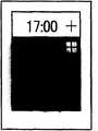
在该移动电话中,作为待机时的显示画面,例如如图17所示,假想在画面的一部分(在图17中,由A示出的上侧)显示时钟等,在其他区域(在图17中,由B示出的区域)显示单色黑画面等的情况。In this mobile phone, as the display screen at the time of standby, for example, as shown in FIG. , the area shown by B) displays a monochromatic black screen or the like.
由于这种情况为待机时,要求以低耗电来显示画面。而且,画面的一部分是黑画面,因而可以通过减小对黑部分的像素写入周期等来进行节电驱动(所谓的部分显示驱动)。Since this is standby, it is required to display a screen with low power consumption. Also, since a part of the screen is a black screen, it is possible to perform power-saving driving (so-called partial display driving) by reducing the pixel writing cycle in the black part or the like.
以下,用图18A~图18D说明部分显示驱动和液晶的交流化。Hereinafter, partial display driving and liquid crystal AC will be described with reference to FIGS. 18A to 18D.
由于液晶不能长时间持续施加直流电场,因此需要按某个周期改变直流电场的方向,即需要所谓的交流化。Since the liquid crystal cannot continue to apply a DC electric field for a long time, it is necessary to change the direction of the DC electric field in a certain period, which requires the so-called AC.
交流化有公共对称法(例如,点反转等)和公共反转法。其中,公共反转法大致分为行反转和帧反转。There are public symmetry methods (for example, point inversion, etc.) and public inversion methods for commutation. Among them, the common inversion method is roughly divided into line inversion and frame inversion.
帧反转在显示的1个垂直期间(帧)进行交流化,而行反转在1个水平期间进行交流化。此处,说明帧反转。Frame inversion performs alternating in one vertical period (frame) of display, while line inversion performs alternating in one horizontal period. Here, frame inversion will be described.
图18A示出部分开始的帧,画面的“+”和“-”,表示向液晶施加了电场方向彼此相反的直流电场。就是说,从“+”到“-”、或从“-”到“+”的变化,表示正在进行交流化。FIG. 18A shows a frame at the beginning of a part, and "+" and "-" on the screen indicate that DC electric fields with opposite electric field directions are applied to the liquid crystal. That is to say, the change from "+" to "-", or from "-" to "+" indicates that communication is in progress.
在图18A中,显示部和黑部都以“+”的方向向像素写入信号。In FIG. 18A , both the display part and the black part write signals to the pixels in the direction of "+".
在图18B中,仅显示部写入视频信号并进行交流化(“-”写入),而黑部分保持在图18A的1帧中写入的像素信号,不对像素进行新的写入。由于不进行新的写入,因此不进行黑部分的交流化而保持原来的“+”的状态。而且,由于不进行新的写入,作为液晶板,耗电量低。In FIG. 18B , only the display portion writes video signals and performs alternating ("-" writing), while the black portion retains the pixel signals written in one frame in FIG. 18A, and no new writing is performed on pixels. Since new writing is not performed, the original "+" state is maintained without alternating the black portion. Furthermore, since new writing is not performed, the power consumption of the liquid crystal panel is low.
在图18C的第3帧中,与图18B的第2帧同样地,黑显示部不进行新的像素写入,而仅使显示部交流化。In the third frame of FIG. 18C , as in the second frame of FIG. 18B , no new pixels are written to the black display portion, and only the display portion is switched to AC.
在图18D的第4帧中,与显示部一致地以“-”的方向对黑部进行新的写入。In the fourth frame of FIG. 18D , new writing is performed in the black portion in the direction of “-” in line with the display portion.
由此,显示部如图18A~图18D所示,在各帧进行交流化,交流化周期为2帧。另一方面,黑部每3帧进行1次交流化,交流化周期为6帧。As a result, the display unit performs alternating in each frame as shown in FIGS. 18A to 18D , and the alternating period is two frames. On the other hand, Kurobe performs communication once every 3 frames, and the communication period is 6 frames.
以下,在本说明书中,将图18A~图18D所示的交流化作为基本的部分显示驱动进行说明。Hereinafter, in this specification, the alternating display shown in FIGS. 18A to 18D will be described as a basic partial display drive.
图19是表示现有的IPS方式的液晶显示板和扫描线驱动电路的概略结构的框图。FIG. 19 is a block diagram showing a schematic configuration of a conventional IPS liquid crystal display panel and scanning line drive circuits.
图19所示的液晶显示板,具有多个子像素。图20表示图19所示的液晶显示板的1个子像素的等效电路。The liquid crystal display panel shown in FIG. 19 has a plurality of sub-pixels. FIG. 20 shows an equivalent circuit of one sub-pixel of the liquid crystal display panel shown in FIG. 19 .
在图20中,COMn是对置电极线(或者也称为公共线),Gn是扫描线(或者也称为栅极线),Sn是视频线(或者也称为源极线、漏极线),TFT是作为有源元件的薄膜晶体管,PIX是像素电极,ITO2是对置电极。In Fig. 20, COMn is the opposite electrode line (or also called the common line), Gn is the scan line (or also called the gate line), Sn is the video line (or also called the source line, the drain line). ), TFT is a thin film transistor as an active element, PIX is a pixel electrode, and ITO2 is a counter electrode.
图19所示的液晶显示板是所谓的IPS方式的液晶显示板,该IPS方式的液晶显示板是像素电极(PIX)和对置电极(ITO2)形成在相同基板上,在像素电极(PIX)和对置电极(ITO2)之间施加电压而在显示部显示图像的方式。The liquid crystal display panel shown in FIG. 19 is a so-called IPS type liquid crystal display panel. In this IPS type liquid crystal display panel, the pixel electrode (PIX) and the counter electrode (ITO2) are formed on the same substrate. A method of displaying images on the display unit by applying a voltage between the counter electrode (ITO2).
在图19所示的液晶显示板中,在每1水平扫描期间,对各扫描线(Gn)供给选择扫描电压。由此,使与各扫描线(Gn)连接 的薄膜晶体管(TFT)在1水平扫描时间的期间导通,并从视频线驱动电路(源极驱动器;SDIV)经视频线(Sn)对各像素电极(PIX)施加与显示数据对应的电压。In the liquid crystal display panel shown in FIG. 19, a selection scanning voltage is supplied to each scanning line (Gn) in each horizontal scanning period. Thus, the thin-film transistor (TFT) connected to each scanning line (Gn) is turned on for one horizontal scanning time, and each pixel is transmitted from the video line driver circuit (source driver; SDIV) via the video line (Sn). The electrodes (PIX) apply voltages corresponding to display data.
另外,给对置电极(ITO2)施加高电平(以下,称为H电平)的公共电压(VCOMH)、或低电平(以下,称为L电平)的公共电压(VCOML)。由此,在液晶显示板上显示图像。Also, a common voltage (VCOMH) at a high level (hereinafter referred to as H level) or a common voltage (VCOML) at a low level (hereinafter referred to as L level) is applied to the counter electrode (ITO2). Thus, an image is displayed on the liquid crystal display panel.
在图19中,T-0~T-n是(n+1)级的移位寄存电路,M 1~M3是晶体管,C-1~C-n+1是(n+1)级的对置电极扫描电路。In Fig. 19, T-0~T-n are (n+1) level shift register circuits,
图21A~图21B是表示图19所示的扫描线驱动电路的时序图。以下,用图21A~图21B简单地说明图19所示的扫描线驱动电路的动作。21A to 21B are timing charts showing the scanning line driving circuit shown in FIG. 19 . Hereinafter, the operation of the scanning line driving circuit shown in FIG. 19 will be briefly described with reference to FIGS. 21A to 21B.
如图21A~图21B所示,对移位寄存电路(T-0~T-n)输入启动脉冲(Vin)和V1、V2的传送时钟信号,从偶数级的移位寄存电路输出与传送时钟信号(V1)同步的移位脉冲,另外,从奇数级的移位寄存电路输出与传送时钟信号(V2)同步的移位脉冲。As shown in FIGS. 21A to 21B , the start pulse (Vin) and the transmission clock signals of V1 and V2 are input to the shift register circuits (T-0 to T-n), and the transmission clock signals ( V1) a synchronized shift pulse, and a shift pulse synchronized with the transfer clock signal (V2) is output from the odd-numbered stages of shift register circuits.
传送时钟信号(V1)和传送时钟信号(V2),周期(此处为2个水平期间)相同、相位相差180°,因此,在每1个水平期间,从移位寄存电路(T-0~T-n)依次输出(Tout-0~Tout-n)的移位脉冲。The transmission clock signal (V1) and the transmission clock signal (V2) have the same period (here, two horizontal periods) and a phase difference of 180°. T-n) sequentially output (Tout-0 ~ Tout-n) shift pulses.
(Tout-0~Tout-n)的移位脉冲,分别施加在各移位级的晶体管(M1)的栅极,晶体管(M1)在被施加(Tout-0~Tout-n)的移位脉冲时导通。The shift pulses of (Tout-0~Tout-n) are respectively applied to the gates of the transistors (M1) of each shift stage, and the transistors (M1) are applied with the shift pulses of (Tout-0~Tout-n) time conduction.
另外,对偶数级的晶体管(M1)的漏极施加传送时钟信号(V1),对奇数级的晶体管(M1)的漏极施加传送时钟信号(V2)。In addition, the transfer clock signal (V1) is applied to the drains of the even-numbered transistors (M1), and the transfer clock signal (V2) is applied to the drains of the odd-numbered transistors (M1).
由此,在每1水平扫描期间,将薄膜晶体管(TFT)导通1个水平期间的选择扫描电压依次输出到扫描线(G1~Gn)。Accordingly, in each horizontal scanning period, the selection scanning voltage in which the thin film transistor (TFT) is turned on for one horizontal period is sequentially output to the scanning lines ( G1 to Gn).
(C-1~C-n+1)的对置电极扫描电路,具有作为给对置电极线(COM1~COMn+1)输出H电平的公共电压(VCOMH)、或 L电平的公共电压(VCOML)的切换开关电路的功能。The opposing electrode scanning circuits (C-1 to C-n+1) have a common voltage (VCOMH) outputting H level or L level common voltage to the opposing electrode lines (COM1 to COMn+1). (VCOML) switch circuit function.
例如,(C-1)的对置电极扫描电路,根据经导通的晶体管(M1、M2)而输入的交流化信号(M)和反转交流化信号(MB),确定输出H电平的公共电压(VCOMH)、或L电平的公共电压(VCOML)中的哪一个,并输入本级的扫描线(此处为扫描线G1)的选择扫描电压作为使能信号(E),从而给对置电极线(COM1~COMn+1)输出H电平的公共电压(VCOMH)、或L电平的公共电压(VCOML)的任一个,其中,上述导通的晶体管是通过前级的扫描线(此处为扫描线G0)的选择扫描电压而导通的。For example, the counter-electrode scanning circuit of (C-1) determines whether to output the H level according to the AC signal (M) and the inverted AC signal (MB) input through the turned-on transistors (M1, M2). common voltage (VCOMH) or L-level common voltage (VCOML), and input the selected scan voltage of the scan line (here, scan line G1) of this stage as the enable signal (E), thus giving Opposite electrode lines (COM1~COMn+1) output either H-level common voltage (VCOMH) or L-level common voltage (VCOML). (Here, the scanning line G0) is turned on by selecting the scanning voltage.
即,如图21A,按每1个水平期间切换交流化信号(M)和反转交流化信号(MB),则H电平的公共电压(VCOMH)、或L电平的公共电压(VCOML)的周期也在1个水平期间中进行切换,成为行反转驱动。That is, as shown in FIG. 21A, the AC signal (M) and the inverted AC signal (MB) are switched every one horizontal period, and the H level common voltage (VCOMH) or the L level common voltage (VCOML) The cycle is also switched in one horizontal period, which becomes row inversion driving.
另外,如图21B,按每1帧切换交流化信号(M)和反转交流化信号(MB),则H电平的公共电压(VCOMH)、或L电平的公共电压(VCOML)的周期也在1帧中进行切换,成为帧反转。In addition, as shown in FIG. 21B, the AC signal (M) and the inverted AC signal (MB) are switched every frame, and the period of the H-level common voltage (VCOMH) or the L-level common voltage (VCOML) Switching is also performed within one frame, which is called frame inversion.
从耗电量的观点来说,交流化信号(M)和反转交流化信号(MB)的频率高的行反转耗电量高,频率低的帧反转耗电量低。From the viewpoint of power consumption, line inversion with high frequencies of the alternating signal (M) and inverted alternating signal (MB) consumes high power, and frame inversion with low frequency consumes low power.
但是,一般来说,帧反转驱动有时会产生串扰而使画质出现问题,因而在通常显示中大多使用行反转。However, in general, frame inversion driving may cause crosstalk and cause image quality problems, so line inversion is often used in normal displays.
此外,例如在下列专利文献1中记载了在上述图18A~图18D中所述的用于实现部分驱动的扫描线驱动电路。In addition, a scanning line driving circuit for realizing partial driving described in the above-mentioned FIGS. 18A to 18D is described in, for example, the following
作为与本申请的发明相关的现有技术文献,有以下的文献。As prior art documents related to the invention of the present application, there are the following documents.
[专利文献1]日本特开2002-351414号公报[Patent Document 1] Japanese Patent Laid-Open No. 2002-351414
[专利文献2]日本特开2005-173244号公报[Patent Document 2] Japanese Unexamined Patent Publication No. 2005-173244
发明内容Contents of the invention
上述专利文献1中所记载的扫描线驱动电路,具有根据移位寄存电路的输出节点的电位依次对扫描线进行扫描驱动的扫描线驱动电路,该扫描线驱动电路,按照非显示区的块的扫描线的扫描时序而输入的输出使能信号XOEV,利用该输出使能信号XOEV进行屏蔽控制,从而实现部分驱动,其中,上述非显示区以所给予的多条扫描线的每1条划分的块为单位而设定的。The scanning line driving circuit described in the above-mentioned
但是,在该专利文献1所记载的扫描线驱动电路中,例如,如IPS方式的液晶显示板等,存在着不能按每1条显示线独立地控制给对置电极线输出的公共电压的问题。However, in the scanning line drive circuit described in
而且,在上述图19所示的扫描驱动电路中,存在着部分显示驱动时的控制很难进行的问题。Furthermore, in the above-mentioned scanning driving circuit shown in FIG. 19, there is a problem that control during partial display driving is difficult.
为进行基本的部分显示驱动,如在图18A~图18D中所述,黑部需要保持3帧期间的像素信号。In order to perform basic partial display driving, as described in FIGS. 18A to 18D , the black portion needs to hold pixel signals for 3 frames.
为保持像素信号,在图18B、图18C的帧的黑部,需要对扫描线输出非选择扫描电压。但是,在图19所示的扫描驱动电路中,不能对扫描线输出非选择扫描电压。In order to hold the pixel signal, it is necessary to output the non-selection scanning voltage to the scanning line in the black portion of the frame in FIG. 18B and FIG. 18C . However, in the scan driving circuit shown in FIG. 19, the non-selection scan voltage cannot be output to the scan lines.
这是因为(V1、V2)的传送时钟信号兼用作移位寄存器的传送信号、选择扫描信号、对置电极扫描电路的动作信号的缘故。This is because the transfer clock signal of (V1, V2) is also used as the transfer signal of the shift register, the selection scanning signal, and the operation signal of the counter electrode scanning circuit.
本发明是为解决上述现有技术的问题而作出的,本发明的优点是可以提供一种在显示装置中,当控制任意区域的显示、非显示时可以降低耗电量的技术。The present invention is made to solve the above-mentioned problems of the prior art. The advantage of the present invention is that it can provide a technology that can reduce power consumption when controlling the display and non-display of an arbitrary area in a display device.
本发明的上述以及其他优点和新颖的特征,通过本说明书的记述和附图得以明确。The above and other advantages and novel features of the present invention will be made clear by the description of this specification and the accompanying drawings.
在本申请书所公开的发明中,如下简单地说明代表性的部分的概要。Among the inventions disclosed in this application, the outline of representative parts will be briefly described as follows.
(1)包括:显示板和驱动上述显示板的驱动电路,上述显示板具有:多个像素;多条扫描线,给上述多个像素施加扫描电压;以及多条信号线,沿上述多条扫描线的延伸方向形成并给上述多个像素施加预定电压,上述驱动电路具有:移位寄存电路,根据所输入的传送时钟信号,在每个预定期间依次输出第1移位脉冲至第n移位脉冲,其中,n≥2;n个第1晶体管,其中,第m个第1晶体 管的栅极被施加从上述移位寄存电路输出的第1移位脉冲至第n移位脉冲中的第m个移位脉冲,这里1≤m≤n;以及n个信号线扫描电路,其中上述传送时钟信号包括第1传送时钟信号、与第1传送时钟信号周期相同而相位不同的第2传送时钟信号,第m个上述第1晶体管,根据第m移位脉冲,对扫描线驱动用时钟信号进行采样,作为第m扫描线用的上述扫描电压输出,这里1≤m≤n,第k信号线扫描电路,当k为奇数时,根据从上述移位寄存电路输出的第(k-1)移位脉冲、交流化信号、反转交流化信号和上述第1传送时钟信号,选择第k信号线用的上述预定电压,根据从上述移位寄存电路输出的第k移位脉冲和上述第2传送时钟信号,输出选定的上述第k信号线用的预定电压,其中,1≤k≤n当k为偶数时,根据从上述移位寄存电路输出的第(k-1)移位脉冲、上述交流化信号、上述反转交流化信号和上述第2传送时钟信号,选择第k信号线用的上述预定电压,根据从上述移位寄存电路输出的第k移位脉冲和上述第1传送时钟信号,输出选定的上述第k信号线用的预定电压,其中,1≤k≤n。(1) Including: a display panel and a driving circuit for driving the above-mentioned display panel, the above-mentioned display panel has: a plurality of pixels; a plurality of scanning lines for applying a scanning voltage to the plurality of pixels; and a plurality of signal lines for scanning along the plurality of pixels The extension direction of the line is formed and a predetermined voltage is applied to the above-mentioned plurality of pixels. The above-mentioned driving circuit has: a shift register circuit, which sequentially outputs the first shift pulse to the n-th shift pulse in each predetermined period according to the input transmission clock signal pulse, wherein, n≥2; n first transistors, wherein the gate of the m first transistor is applied to the first shift pulse output from the above-mentioned shift register circuit to the first shift pulse in the nth shift pulse m shift pulses, where 1≤m≤n; and n signal line scanning circuits, wherein the transmission clock signal includes a first transmission clock signal and a second transmission clock signal having the same cycle as the first transmission clock signal but a different phase , the mth above-mentioned first transistor samples the clock signal for driving the scanning line according to the mth shift pulse, and outputs it as the above-mentioned scanning voltage for the mth scanning line, where 1≤m≤n, the kth signal line scans A circuit for selecting the kth signal line based on the (k-1)th shift pulse output from the shift register circuit, the alternating signal, the inverted alternating signal, and the first transmission clock signal when k is an odd number. The predetermined voltage for the above-mentioned k-th signal line is output according to the k-th shift pulse output from the above-mentioned shift register circuit and the above-mentioned second transmission clock signal, wherein, 1≤k≤n when k When it is an even number, the above-mentioned signal line for the k-th signal line is selected based on the (k-1)th shift pulse output from the above-mentioned shift register circuit, the above-mentioned AC signal, the above-mentioned inverted AC signal, and the above-mentioned second transfer clock signal. A predetermined voltage for outputting a selected predetermined voltage for the kth signal line based on the kth shift pulse output from the shift register circuit and the first transfer clock signal, where 1≤k≤n.
(2)在(1)中,还包括:n个第2晶体管,其中,第m个第2晶体管的栅极被施加从上述移位寄存电路输出的第1移位脉冲至第n移位脉冲中的第m个移位脉冲,这里1≤m≤n;以及n个第3晶体管和n个第4晶体管,其中,在各信号线扫描电路的每一个上设置该n个第3晶体中的一个,在各信号线扫描电路的每一个上设置该n个第4晶体中的一个,第k个第2晶体管,根据从第k移位寄存电路输出的移位脉冲,对上述第1传送时钟信号或第2传送时钟信号进行采样,作为使能信号输入到第k信号线扫描电路,第k个第3晶体管,根据由第(k-1)个第2晶体管采样后的传送时钟信号,对上述交流化信号进行采样,输入到第k信号线扫描电路,第k个第4晶体管,根据由第(k-1)个第2晶体管采样后的传送时钟信号,对上述反转交流化信号进行采样,输入到第k信号线扫描电路,其中1≤k≤n。(2) In (1), further comprising: n second transistors, wherein the gate of the mth second transistor is applied with the first shift pulse to the nth shift pulse output from the shift register circuit The mth shift pulse in , where 1≤m≤n; and n third transistors and n fourth transistors, wherein each of the n third crystals is set on each signal line scanning circuit One, one of the n 4th crystals is set on each of the signal line scanning circuits, and the kth 2nd transistor, according to the shift pulse output from the kth shift register circuit, controls the above-mentioned 1st transfer clock Signal or the 2nd transmission clock signal is sampled, input to the kth signal line scanning circuit as an enable signal, the kth 3rd transistor, according to the transmission clock signal sampled by the (k-1)th 2nd transistor, to The above-mentioned AC signal is sampled, input to the k-th signal line scanning circuit, the k-th fourth transistor, according to the transmission clock signal sampled by the (k-1)-th second transistor, the above-mentioned inverted AC signal is performed Sampling is input to the kth signal line scanning circuit, where 1≤k≤n.
(3)在(2)中,上述传送时钟信号是周期相同、相位不同的第1传送时钟信号和第2传送时钟信号,相互邻接的2个第2晶体管中的一个,对上述第1传送时钟信号进行采样,上述相互邻接的2个第2晶体管中的另一个,对上述第2传送时钟信号进行采样。(3) In (2), the transmission clock signal is the first transmission clock signal and the second transmission clock signal having the same cycle and different phases, and one of the two second transistors adjacent to each other responds to the first transmission clock signal. The signal is sampled, and the other of the two adjacent second transistors samples the second transfer clock signal.
(4)在(1)~(3)的任何一项中,上述扫描线驱动用时钟信号是周期相同、相位不同的第1扫描线驱动用时钟信号和第2扫描线驱动用时钟信号,相互邻接的2个第1晶体管中的一个,对上述第1扫描线驱动用时钟信号进行采样,上述相互邻接的2个第1晶体管中的另一个,对上述第2扫描线驱动用时钟信号进行采样。(4) In any one of (1) to (3), the clock signal for driving the scanning line is the first clock signal for driving the scanning line and the second clock signal for driving the scanning line, which have the same cycle and different phases, and are mutually independent. One of the two adjacent first transistors samples the clock signal for driving the first scan line, and the other of the two adjacent first transistors samples the clock signal for driving the second scan line. .
(5)在(1)至(4)的任何一项中,上述扫描线驱动用时钟信号,在1帧期间内,具有固定为第1电压电平或第2电压电平的切断期间。(5) In any one of (1) to (4), the scanning line driving clock signal has an off period fixed at the first voltage level or the second voltage level within one frame period.
(6)包括:显示板和驱动上述显示板的驱动电路,上述显示板具有:多个像素;多条扫描线,给上述多个像素施加扫描电压;以及多条信号线,沿上述多条扫描线的延伸方向形成并给上述多个像素施加预定电压,上述驱动电路具有:移位寄存电路,根据所输入的传送时钟信号,在每个预定期间依次输出第1移位脉冲至第n移位脉冲,其中,n≥2;n个第1晶体管和n个第2晶体管,其中,第m个第1晶体管和第m个第2晶体管的栅极被施加从上述移位寄存电路输出的第1移位脉冲至第n移位脉冲中的第m个移位脉冲,这里1≤m≤n;以及2n个信号线扫描电路,上述传送时钟信号包括第1传送时钟信号、与第1传送时钟信号周期相同而相位不同的第2传送时钟信号,第k个第1晶体管,根据从上述移位寄存电路输出的第k移位脉冲,对第1扫描线驱动用时钟信号进行采样,作为第(2k-1)扫描线用的上述扫描电压输出,其中1≤k≤n,第k个第2晶体管,根据从上述移位寄存电路输出的第k移位脉冲,对周期与上述第1扫描线驱动用时钟信号相同而相位不同的第2扫描线驱动用时钟信号进行采样,作为第2k扫描线用的上述扫描电压 输出,当k为偶数时,第(2k-1)信号线扫描电路和第2k信号线扫描电路,根据从上述移位寄存电路输出的第(k-1)移位脉冲、交流化信号、反转交流化信号和上述第1传送时钟信号,选择第(2k-1)信号线用的上述预定电压和第2k信号线用的上述预定电压,根据从上述移位寄存电路输出的第k移位脉冲和上述第2传送时钟信号输出选定的上述第(2k-1)信号线用的预定电压和上述第2k信号线用的上述预定电压,当k为奇数时,第(2k-1)信号线扫描电路和第2k信号线扫描电路,根据从上述移位寄存电路输出的第(k-1)移位脉冲、上述交流化信号、上述反转交流化信号和上述第2传送时钟信号,选择第(2k-1)信号线用的上述预定电压和第2k信号线用的上述预定电压,根据从上述移位寄存电路输出的第k移位脉冲和上述第1传送时钟信号输出选定的上述第(2k-1)信号线用的预定电压和上述第2k信号线用的预定电压。(6) Including: a display panel and a driving circuit for driving the above-mentioned display panel, the above-mentioned display panel has: a plurality of pixels; a plurality of scanning lines for applying a scanning voltage to the plurality of pixels; and a plurality of signal lines for scanning along the plurality of pixels The extension direction of the line is formed and a predetermined voltage is applied to the above-mentioned plurality of pixels. The above-mentioned driving circuit has: a shift register circuit, which sequentially outputs the first shift pulse to the n-th shift pulse in each predetermined period according to the input transmission clock signal Pulse, where n≥2; n first transistors and n second transistors, wherein the gates of the m first transistor and the m second transistor are applied with the first output from the shift register circuit a shift pulse to an m-th shift pulse among the n-th shift pulses, where 1≤m≤n; and 2n signal line scanning circuits, the above-mentioned transmission clock signal includes a first transmission clock signal, and a first transmission clock signal The second transmission clock signal with the same period and different phases, the kth first transistor samples the first scanning line driving clock signal according to the kth shift pulse output from the above-mentioned shift register circuit, as the (2kth) -1) The above-mentioned scan voltage output for the scan line, wherein 1≤k≤n, the k-th second transistor, according to the k-th shift pulse output from the above-mentioned shift register circuit, drives the period and the above-mentioned first scan line Sampling with the clock signal for driving the second scan line with the same clock signal and different phases, as the above-mentioned scan voltage output for the 2k scan line, when k is an even number, the (2k-1) signal line scan circuit and the 2k scan line The signal line scanning circuit selects the (2k-1)th signal line based on the (k-1)th shift pulse output from the above-mentioned shift register circuit, the AC signal, the inverted AC signal, and the above-mentioned first transfer clock signal The above-mentioned predetermined voltage for use and the above-mentioned predetermined voltage for the 2kth signal line are output from the above-mentioned (2k-1)th signal line selected based on the k-th shift pulse output from the above-mentioned shift register circuit and the above-mentioned second transfer clock signal The predetermined voltage used and the above-mentioned predetermined voltage used for the above-mentioned 2k signal line, when k is an odd number, the (2k-1) signal line scanning circuit and the 2k signal line scanning circuit, according to the output from the above-mentioned shift register circuit (k-1) shift pulse, the above-mentioned AC signal, the above-mentioned inverted AC signal and the above-mentioned second transmission clock signal, select the above-mentioned predetermined voltage for the (2k-1)th signal line and the above-mentioned voltage for the 2kth signal line The predetermined voltage is a predetermined voltage for the (2k-1)th signal line and a predetermined voltage for the 2kth signal line selected based on the kth shift pulse output from the shift register circuit and the first transfer clock signal. Voltage.
(7)在(6)中,还包括:n个第3晶体管,其中,第m个第3晶体管的栅极被施加从上述移位寄存电路输出的第1移位脉冲至第n移位脉冲中的第m个移位脉冲,这里1≤m≤n;2n个第4晶体管和2n个第5晶体管,其中,在各信号线扫描电路的每一个上设置该2n个第4晶体中的1个,在各信号线扫描电路的每一个上设置该2n个第5晶体中的1个,第k个第3晶体管,根据从上述移位寄存电路输出的第k移位脉冲,对上述第1传送时钟信号和上述第2传送时钟信号进行采样,并且作为使能信号输入到上述第(2k-1)信号线扫描电路和第2k信号线扫描电路,第(2k-1)个第4晶体管,根据由第(k-1)个第3晶体管采样后的传送时钟信号,对上述交流化信号进行采样,输入到上述第(2k-1)信号线扫描电路,第(2k-1)个第5晶体管,根据由上述第(k-1)个第3晶体管采样后的传送时钟信号,对上述反转交流化信号进行采样,输入到上述第(2k-1)信号线扫描电路,第2k个第4晶体管,根据由上述第(k-1)个第3晶体管采样后的传送时钟信号,对上述交流化信号进行采样,输入到上述第2k信号线扫描电路,第2k个第5 晶体管,根据由上述第(k-1)个第3晶体管采样后的传送时钟信号,对上述反转交流化信号进行采样,输入到上述第2k信号线扫描电路。(7) In (6), further comprising: n third transistors, wherein the gate of the mth third transistor is applied with the first shift pulse to the nth shift pulse output from the shift register circuit The mth shift pulse in , where 1≤m≤n; 2n 4th transistors and 2n 5th transistors, wherein 1 of the 2n 4th crystals is set on each of the signal line scanning circuits One of the 2n 5th crystals is set on each of the signal line scanning circuits, and the kth 3rd transistor, according to the kth shift pulse output from the above-mentioned shift register circuit, is used for the above-mentioned first The transmission clock signal and the above-mentioned 2nd transmission clock signal are sampled, and are input as an enable signal to the above-mentioned (2k-1)th signal line scanning circuit and the 2kth signal line scanning circuit, the (2k-1)th fourth transistor, According to the transmission clock signal sampled by the (k-1)th 3rd transistor, the above-mentioned AC signal is sampled and input to the above-mentioned (2k-1) signal line scanning circuit, and the (2k-1)th 5th Transistors, according to the transmission clock signal sampled by the (k-1)th third transistor, sample the above-mentioned inverted AC signal, input to the above-mentioned (2k-1)th signal line scanning circuit, the 2kth 4 transistors, according to the transmission clock signal sampled by the above-mentioned (k-1) 3rd transistor, the above-mentioned AC signal is sampled, input to the above-mentioned 2k signal line scanning circuit, the 2k 5th transistor, according to The transfer clock signal sampled by the (k-1)th third transistor samples the inverted AC signal and inputs it to the 2kth signal line scanning circuit.
(8)在(7)中,上述传送时钟信号是周期相同、相位不同的第1传送时钟信号和第2传送时钟信号,相互邻接的2个第3晶体管中的一个,对上述第1传送时钟信号进行采样,上述相互邻接的2个第3晶体管中的另一个,对上述第2传送时钟信号进行采样。(8) In (7), the transmission clock signal is the first transmission clock signal and the second transmission clock signal having the same cycle and different phases, and one of the two third transistors adjacent to each other responds to the first transmission clock signal. The signal is sampled, and the other of the two adjacent third transistors samples the second transfer clock signal.
(9)包括显示板和驱动上述显示板的驱动电路,上述显示板具有:多个像素;多条扫描线,给上述多个像素施加扫描电压;以及多条信号线,沿上述多条扫描线的延伸方向形成并给上述多个像素施加预定电压,上述驱动电路具有:移位寄存电路,根据所输入的传送时钟信号,在每个预定期间依次输出第1移位脉冲至第n移位脉冲,其中n≥2;n个第1晶体管和n个第2晶体管,其中,第m个第1晶体管和第m个第2晶体管的栅极被施加从上述移位寄存电路输出的第1移位脉冲至第n移位脉冲中的第m个移位脉冲,这里1≤m≤n;以及2n个信号线扫描电路,第k个第1晶体管,其中1≤k≤n,根据从上述移位寄存电路输出的第k移位脉冲,对第1扫描线驱动用时钟信号进行采样,作为第(2k-1)扫描线用的上述扫描电压输出,第k个第2晶体管,根据从上述移位寄存电路输出的第k移位脉冲,对周期与上述第1扫描线驱动用时钟信号相同而相位不同的第2扫描线驱动用时钟信号进行采样,作为第2k扫描线用的上述扫描电压输出,第(2k-1)信号线扫描电路,根据从上述移位寄存电路输出的第(k-1)移位脉冲、交流化信号、反转交流化信号、和第2信号线驱动用时钟信号,选择第(2k-1)信号线用的上述预定电压,根据从上述移位寄存电路输出的第k移位脉冲和与上述第2信号线驱动用时钟信号周期相同相位不同的第1信号线驱动用时钟信号输出选定的上述第(2k-1)信号线用的预定电压,第2k信号线扫描电路,根据从上述移位寄存电路输出的第k移位脉冲、上述交流化信号、上述反转交流化信号和上述第1信 号线驱动用时钟信号,选择第2k信号线用的上述预定电压,根据从上述移位寄存电路输出的第k移位脉冲和上述第2信号线驱动用时钟信号,输出选定的上述第2k信号线用的预定电压。(9) including a display panel and a drive circuit for driving the display panel, the display panel has: a plurality of pixels; a plurality of scanning lines for applying a scanning voltage to the plurality of pixels; and a plurality of signal lines along the plurality of scanning lines The extension direction is formed and a predetermined voltage is applied to the above-mentioned plurality of pixels. The above-mentioned driving circuit has: a shift register circuit, which sequentially outputs the first shift pulse to the n-th shift pulse in each predetermined period according to the input transmission clock signal , where n≥2; n first transistors and n second transistors, wherein the gates of the m first transistor and the m second transistor are applied with the first shift output from the above shift register circuit pulse to the m-th shift pulse in the n-th shift pulse, where 1≤m≤n; and 2n signal line scanning circuits, the k-th 1st transistor, where 1≤k≤n, according to the shift from the above The kth shift pulse output by the register circuit samples the clock signal for driving the first scanning line, and outputs it as the above-mentioned scanning voltage for the (2k-1)th scanning line. The kth shift pulse output by the register circuit samples the second scanning line driving clock signal having the same cycle as the first scanning line driving clock signal but different in phase, and outputs it as the scanning voltage for the 2k scanning line, The (2k-1)th signal line scanning circuit is based on the (k-1)th shift pulse output from the shift register circuit, the alternating signal, the inverted alternating signal, and the clock signal for driving the second signal line, Select the above-mentioned predetermined voltage for the (2k-1)th signal line, and drive the first signal line based on the k-th shift pulse output from the above-mentioned shift register circuit and the first signal line having the same period as the clock signal for driving the second signal line and having a different phase. A clock signal is used to output the predetermined voltage for the selected (2k-1)th signal line, and the 2kth signal line scanning circuit, based on the kth shift pulse output from the above-mentioned shift register circuit, the above-mentioned alternating signal, and the above-mentioned inverted Convert the AC signal and the above-mentioned first signal line driving clock signal, select the above-mentioned predetermined voltage for the 2k signal line, and select the above-mentioned predetermined voltage according to the k shift pulse output from the above-mentioned shift register circuit and the above-mentioned 2nd signal line driving clock signal signal to output a predetermined voltage for the selected 2kth signal line.
(10)在(9)中,还包括:n个第3晶体管和n个第4晶体管,其中,第m个第3晶体管和第m个第4晶体管的栅极被施加从上述移位寄存电路输出的第1移位脉冲至第n移位脉冲中的第m个移位脉冲,这里1≤m≤n;以及2n个第5晶体管和2n个第6晶体管,其中,在各信号线扫描电路的每一个上设置该2n个第5晶体中的1个,在各信号线扫描电路的每一个上设置该2n个第6晶体中的1个,第k个第3晶体管,根据从上述移位寄存电路输出的第k移位脉冲,对上述第1信号线驱动用时钟信号进行采样,作为使能信号输入到上述第(2k-1)信号线扫描电路,第k个第4晶体管,根据从上述移位寄存电路输出的第k移位脉冲,对上述第2信号线驱动用时钟信号进行采样,作为使能信号输入到上述第2k信号线扫描电路,第(2k-1)个第5晶体管,根据由第(k-1)个第4晶体管采样后的上述第2信号线驱动用时钟信号,对上述交流化信号进行采样,输入到上述第(2k-1)信号线扫描电路,第(2k-1)个第6晶体管,根据由上述第(k-1)个第4晶体管采样后的上述第2信号线驱动用时钟信号,对上述反转交流化信号进行采样,输入到上述第(2k-1)信号线扫描电路,第2k个第5晶体管,根据由上述第k个第3晶体管采样后的上述第1信号线驱动用时钟信号,对上述交流化信号进行采样,输入到上述第2k信号线扫描电路,第2k个第6晶体管,根据由上述第k个第3晶体管采样后的上述第1信号线驱动用时钟信号,对上述反转交流化信号进行采样,输入到上述第2k信号线扫描电路。(10) In (9), it also includes: n 3rd transistors and n 4th transistors, wherein the gates of the m 3rd transistors and the m 4th transistors are applied from the shift register circuit The m-th shift pulse in the outputted 1st shift pulse to the n-th shift pulse, where 1≤m≤n; and 2n fifth transistors and 2n sixth transistors, wherein the scanning circuit on each signal line One of the 2n fifth crystals is set on each of the signal line scanning circuits, one of the 2n sixth crystals is set on each of the signal line scanning circuits, and the kth third transistor is shifted from the above The kth shift pulse output by the register circuit samples the above-mentioned first signal line driving clock signal, and inputs it to the above-mentioned (2k-1) signal line scanning circuit as an enable signal, and the kth fourth transistor, according to The kth shift pulse output by the above-mentioned shift register circuit samples the above-mentioned second signal line driving clock signal, and inputs it to the above-mentioned 2k signal line scanning circuit as an enable signal, and the (2k-1)th fifth transistor , according to the clock signal for driving the second signal line sampled by the (k-1)th 4th transistor, the above-mentioned AC signal is sampled, and input to the above-mentioned (2k-1)th signal line scanning circuit, the ( 2k-1) 6th transistors sample the inverted AC signal based on the clock signal for driving the second signal line sampled by the (k-1) 4th transistor, and input it to the ( 2k-1) A signal line scanning circuit, wherein the 2kth fifth transistor samples the AC signal based on the clock signal for driving the first signal line sampled by the kth third transistor, and inputs the above-mentioned AC signal to the above-mentioned kth third transistor. In the 2k signal line scanning circuit, the 2kth 6th transistor samples the above-mentioned inverted AC signal based on the clock signal for driving the first signal line sampled by the above-mentioned kth 3rd transistor, and inputs it to the above-mentioned 2kth transistor. Signal line scanning circuit.
(11)在(6)~(10)的任何一项中,上述第1扫描线驱动用时钟信号和第2扫描线驱动用时钟信号,在1帧期间内,具有固定为第1电压电平或第2电压电平的切断期间。(11) In any one of (6) to (10), the clock signal for driving the first scanning line and the clock signal for driving the second scanning line have a fixed voltage level at the first voltage level in one frame period. Or the cut-off period of the second voltage level.
(12)包括显示板和驱动上述显示板的驱动电路,上述显示板 具有:多个像素;多条扫描线,给上述多个像素施加扫描电压;以及多条信号线,沿上述多条扫描线的延伸方向形成并给上述多个像素施加预定电压,上述驱动电路具有:移位寄存电路,根据所输入的传送时钟信号在每个预定期间依次输出第1移位脉冲至第n移位脉冲,其中,n≥2;n个第1晶体管和n个第2晶体管,其中,第m个第1晶体管和第m个第2晶体管的栅极被施加从上述移位寄存电路输出的第1移位脉冲至第n移位脉冲中的第m个移位脉冲,这里1≤m≤n;n个第3晶体管和n个第4晶体管,分别在栅极施加选择信号;n个第5晶体管和n个第6晶体管,分别在栅极施加反转选择信号;以及2n个信号线扫描电路,第k个第1晶体管,根据从上述移位寄存电路输出的第k移位脉冲,对第1扫描线驱动用时钟信号进行采样,作为第(2k-1)扫描线用的上述扫描电压输出,其中1≤k≤n,第k个第2晶体管,根据从上述移位寄存电路输出的第k移位脉冲,对周期与上述第1扫描线驱动用时钟信号相同而相位不同的第2扫描线驱动用时钟信号进行采样,作为第2k扫描线用的上述扫描电压输出,第k个第3晶体管,根据上述选择信号,将由第k个第1晶体管采样后的上述第1扫描线驱动用时钟信号作为使能信号输入到第(2k-1)信号线扫描电路,第k个第4晶体管,根据上述选择信号,将由第k个第2晶体管采样后的上述第2扫描线驱动用时钟信号作为使能信号输入到第2k信号线扫描电路,第k个第5晶体管,根据上述反转选择信号,将从上述移位寄存电路输出的第k移位脉冲作为使能信号输入到第(2k-1)信号线扫描电路,第k个第6晶体管,根据上述反转选择信号,将从上述移位寄存电路输出的第k移位脉冲作为使能信号输入到第2k信号线扫描电路,第(2k-1)信号线扫描电路,根据从第(k-1)移位寄存电路输出的移位脉冲、第1交流化信号、反转第1交流化信号,选择第(2k-1)信号线用的上述预定电压,根据上述第1扫描线驱动用时钟信号或从上述移位寄存电路输出的第k移位脉冲,输出选定的上述第(2k-1)信号线用的预定电压,(12) Including a display panel and a driving circuit for driving the above-mentioned display panel, the above-mentioned display panel has: a plurality of pixels; a plurality of scanning lines for applying a scanning voltage to the plurality of pixels; and a plurality of signal lines along the plurality of scanning lines The extension direction is formed and a predetermined voltage is applied to the plurality of pixels. The above-mentioned driving circuit has: a shift register circuit, which sequentially outputs the first shift pulse to the n-th shift pulse in each predetermined period according to the input transmission clock signal, Wherein, n≥2; n first transistors and n second transistors, wherein the gates of the mth first transistor and the mth second transistor are applied with the first shift output from the above-mentioned shift register circuit pulse to the mth shift pulse in the nth shift pulse, where 1≤m≤n; n third transistors and n fourth transistors respectively apply selection signals to the gates; n fifth transistors and n The 6th transistor applies an inversion selection signal to the gate respectively; and 2n signal line scanning circuits, the kth 1st transistor, according to the kth shift pulse output from the above-mentioned shift register circuit, to the 1st scanning line The clock signal for driving is sampled and output as the above-mentioned scanning voltage for the (2k-1)th scanning line, where 1≤k≤n, the k-th second transistor is shifted according to the k-th shift output from the above-mentioned shift register circuit Pulse, sampling the second scanning line driving clock signal with the same period as the first scanning line driving clock signal but different in phase, and outputting it as the above scanning voltage for the 2k scanning line, the kth third transistor, according to The above-mentioned selection signal is input to the (2k-1) signal line scanning circuit as an enable signal by the above-mentioned first scanning line driving clock signal sampled by the k-th first transistor, and the k-th fourth transistor, according to the above-mentioned selection signal, the clock signal for driving the second scanning line sampled by the kth second transistor is input to the 2kth signal line scanning circuit as an enable signal, and the kth fifth transistor, according to the above-mentioned inversion selection signal, will be from The kth shift pulse output by the above-mentioned shift register circuit is input to the (2k-1) signal line scanning circuit as an enable signal, and the kth sixth transistor, according to the above-mentioned inverting selection signal, will switch from the above-mentioned shift register circuit to The outputted kth shift pulse is input to the 2kth signal line scanning circuit as an enable signal, and the (2k-1)th signal line scanning circuit, according to the shift pulse outputted from the (k-1)th shift register circuit, the th 1 alternating signal, inverting the first alternating signal, selecting the above-mentioned predetermined voltage for the (2k-1)th signal line, shifting according to the clock signal for driving the first scanning line or the k-th shift outputted from the above-mentioned shift register circuit bit pulse, outputting a predetermined voltage for the selected above-mentioned (2k-1)th signal line,
第2k信号线扫描电路,根据从第(k-1)移位寄存电路输出的移位脉冲、第2交流化信号、和反转第2交流化信号,选择第2k信号线用的上述预定电压,根据上述第2扫描线驱动用时钟信号或从上述移位寄存电路输出的第k移位脉冲,输出选定的上述第2k信号线用的预定电压。The 2k signal line scanning circuit selects the above-mentioned predetermined voltage for the 2k signal line based on the shift pulse output from the (k-1)th shift register circuit, the second AC signal, and the inverted second AC signal. and outputting a predetermined voltage for the selected 2kth signal line based on the clock signal for driving the second scanning line or the kth shift pulse outputted from the shift register circuit.
(13)在(12)中,还包括:2n个第7晶体管和2n个第8晶体管,其中,在各信号线扫描电路的每一个上设置该2n个第7晶体中的1个,在各信号线扫描电路的每一个上设置该2n个第8晶体中的1个,第(2k-1)个第7晶体管,根据从上述移位寄存电路输出的第(k-1)移位脉冲,对上述第1交流化信号进行采样,输入到上述第(2k-1)信号线扫描电路,第(2k-1)个第8晶体管,根据从上述移位寄存电路输出的第(k-1)移位脉冲,对上述反转第1交流化信号进行采样,输入到上述第(2k-1)信号线扫描电路,第2k个第7晶体管,根据从上述移位寄存电路输出的第(k-1)移位脉冲,对上述第2交流化信号进行采样,输入到上述第2k信号线扫描电路,第2k个第8晶体管,根据从上述移位寄存电路输出的第(k-1)移位脉冲,对上述反转第2交流化信号进行采样,输入到上述第2k信号线扫描电路。。(13) In (12), further comprising: 2n 7th transistors and 2n 8th transistors, wherein one of the 2n 7th transistors is provided on each signal line scanning circuit, and each Each of the signal line scanning circuits is provided with one of the 2n eighth crystals, the (2k-1)th seventh transistor, according to the (k-1)th shift pulse output from the above-mentioned shift register circuit, The above-mentioned 1st AC signal is sampled, input to the above-mentioned (2k-1) signal line scanning circuit, the (2k-1) 8th transistor, according to the (k-1)th output from the above-mentioned shift register circuit The shift pulse samples the above-mentioned inverted first AC signal, and inputs it to the above-mentioned (2k-1) signal line scanning circuit, and the 2kth 7th transistor, according to the (k-th 1) shift pulse, sample the above-mentioned 2nd AC signal, input to the above-mentioned 2k signal line scanning circuit, the 2k 8th transistor, according to the (k-1)th shift outputted from the above-mentioned shift register circuit The pulse is used to sample the above-mentioned inverted second AC signal, and input it to the above-mentioned 2k signal line scanning circuit. .
(14)在(13)中,上述传送时钟信号是周期相同、相位不同的第1传送时钟信号和第2传送时钟信号。(14) In (13), the transmission clock signal is a first transmission clock signal and a second transmission clock signal having the same cycle and different phases.
(15)在(12)~(14)的任何一项中,上述第1扫描线驱动用时钟信号和第2扫描线驱动用时钟信号,在1帧期间内,具有固定为第1电压电平或第2电压电平的切断期间。(15) In any one of (12) to (14), the clock signal for driving the first scanning line and the clock signal for driving the second scanning line have a fixed voltage level at the first voltage level in one frame period. Or the cut-off period of the second voltage level.
(16)在(15)中,当上述第1扫描线驱动用时钟信号和第2扫描线驱动用时钟信号为上述切断期间时,上述选择信号为第3电压电平,上述反转选择信号为第4电压电平,在上述第1扫描线驱动用时钟信号和第2扫描线驱动用时钟信号为上述切断期间以外的期间,上述选择信号为上述第4电压电平,上述反转选择信号为上述第3电压电平。(16) In (15), when the clock signal for driving the first scanning line and the clock signal for driving the second scanning line are in the off-period, the selection signal is at the third voltage level, and the inversion selection signal is At the fourth voltage level, when the clock signal for driving the first scanning line and the clock signal for driving the second scanning line are in periods other than the cut-off period, the selection signal is at the fourth voltage level, and the inverted selection signal is above the 3rd voltage level.
(17)在(15)或(16)中,当上述第1扫描线驱动用时钟信号和第2扫描线驱动用时钟信号为上述切断期间时,上述第1交流化信号和上述第2交流化信号是相位相同的信号。(17) In (15) or (16), when the clock signal for driving the first scan line and the clock signal for driving the second scan line are in the off period, the first AC signal and the second AC signal The signals are signals with the same phase.
(18)在(12)~(17)的任何一项中,在通常的显示期间,上述第1交流化信号和上述第2交流化信号是相位相反的信号,在部分显示期间时,上述第1交流化信号和上述第2交流化信号,是相位相同的信号。(18) In any one of (12) to (17), during the normal display period, the first alternating signal and the second alternating signal are signals with opposite phases, and during the partial display period, the first alternating signal The first alternating signal and the above-mentioned second alternating signal are signals having the same phase.
(19)在(5)、(11)、(12)~(17)的任何一项中,上述切断期间中的上述传送时钟信号的振幅电平,小于上述切断期间以外的期间中的上述传送时钟信号的振幅电平。(19) In any one of (5), (11), (12) to (17), the amplitude level of the transmission clock signal during the off period is smaller than that of the transmission clock signal during periods other than the off period. The amplitude level of the clock signal.
(20)在(1)~(19)的任何一项中,上述信号线是对置电极线,上述预定电压是第1电压电平的对置电压和第2电压电平的对置电压。(20) In any one of (1) to (19), the signal line is an opposing electrode line, and the predetermined voltage is an opposing voltage at a first voltage level and an opposing voltage at a second voltage level.
(21)在(1)~(19)的任何一项中,上述信号线是对各像素施加补偿电压的补偿信号线。(21) In any one of (1) to (19), the signal line is a compensation signal line for applying a compensation voltage to each pixel.
在本申请书所公开的发明中,如简单地说明由代表性的部分取得的效果,则如下所述。Among the inventions disclosed in this application, the effects obtained by representative parts will be briefly described as follows.
按照本发明的显示装置,当控制任意区域的显示、非显示时,可以实现耗电量的减低。According to the display device of the present invention, when controlling the display and non-display of an arbitrary area, it is possible to reduce power consumption.
附图说明Description of drawings
图1是表示本发明的实施例1的扫描线驱动电路的概略结构的框图。FIG. 1 is a block diagram showing a schematic configuration of a scanning line driving circuit according to
图2是表示图1所示的扫描线驱动电路中的部分显示驱动时的1帧内的时序图。FIG. 2 is a timing chart showing a part of display driving in one frame in the scanning line driving circuit shown in FIG. 1 .
图3是表示图1所示的扫描线驱动电路中的包含通常显示驱动的部分显示驱动的5帧大小的时序图。3 is a timing chart showing five frames of partial display driving including normal display driving in the scanning line driving circuit shown in FIG. 1 .
图4是表示图1所示的扫描线驱动电路的变形例中的部分显示驱动时的1帧内的时序图。4 is a timing chart showing a partial display drive in one frame in a modified example of the scanning line driving circuit shown in FIG. 1 .
图5是表示本发明的实施例2的扫描线驱动电路的概略结构的框图。5 is a block diagram showing a schematic configuration of a scanning line driving circuit according to
图6是表示图5所示的扫描线驱动电路中的部分显示驱动时的1帧内的时序图。FIG. 6 is a timing chart showing a part of display driving in one frame in the scanning line driving circuit shown in FIG. 5 .
图7是表示图5所示的扫描线驱动电路中的包含通常显示驱动的部分显示驱动的5帧大小的时序图。FIG. 7 is a timing chart showing five frames of partial display driving including normal display driving in the scanning line driving circuit shown in FIG. 5 .
图8是表示本发明的实施例3的扫描线驱动电路的概略结构的框图。8 is a block diagram showing a schematic configuration of a scanning line driving circuit according to
图9是表示图8所示的扫描线驱动电路中的部分显示驱动时的1帧内的时序图。FIG. 9 is a timing chart showing partial display driving in one frame in the scanning line driving circuit shown in FIG. 8 .
图10是表示图8所示的扫描线驱动电路中的包含通常显示驱动的部分显示驱动的5帧大小的时序图。FIG. 10 is a timing chart showing five frames of partial display driving including normal display driving in the scanning line driving circuit shown in FIG. 8 .
图11是表示本发明的实施例4的扫描线驱动电路的概略结构的框图。11 is a block diagram showing a schematic configuration of a scanning line driving circuit according to
图12是表示图11所示的扫描线驱动电路中的部分显示驱动时的1帧内的时序图。FIG. 12 is a timing chart showing a part of display driving in one frame in the scanning line driving circuit shown in FIG. 11 .
图13是表示图11所示的扫描线驱动电路中的包含通常显示驱动的部分显示驱动的5帧大小的时序图。FIG. 13 is a timing chart showing five frames of partial display driving including normal display driving in the scanning line driving circuit shown in FIG. 11 .
图14是表示独立电容耦合(Charge-Coupling:电荷耦合)驱动液晶显示板的1个子像素的等效电路的电路图。14 is a circuit diagram showing an equivalent circuit of one sub-pixel of a liquid crystal display panel driven by independent capacitive coupling (Charge-Coupling).
图15是表示驱动现有的独立电容耦合(Charge-Coupling:电荷耦合)驱动液晶显示板的扫描线驱动电路的概略结构的框图。15 is a block diagram showing a schematic configuration of a scanning line drive circuit for driving a conventional independent capacitive coupling (Charge-Coupling: charge-coupled) drive liquid crystal display panel.
图16是表示图15所示的扫描线驱动电路的时序图。FIG. 16 is a timing chart showing the scanning line driving circuit shown in FIG. 15 .
图17是表示移动电话的待机画面的图。Fig. 17 is a diagram showing a standby screen of a mobile phone.
图18A~图18D是说明液晶显示装置中的部分显示驱动和液晶的交流化的图。18A to 18D are diagrams illustrating partial display driving and alternating liquid crystal in a liquid crystal display device.
图19是表示现有的IPS方式的液晶显示板和扫描线驱动电路的概略结构的框图。FIG. 19 is a block diagram showing a schematic configuration of a conventional IPS liquid crystal display panel and scanning line drive circuits.
图20是表示图19所示的液晶显示板的1个子像素的等效电路的图。FIG. 20 is a diagram showing an equivalent circuit of one sub-pixel of the liquid crystal display panel shown in FIG. 19 .
图21A~图21B是表示图19所示的扫描线驱动电路的时序图。21A to 21B are timing charts showing the scanning line driving circuit shown in FIG. 19 .
具体实施方式Detailed ways
以下,参照附图详细说明本发明的实施例。Hereinafter, embodiments of the present invention will be described in detail with reference to the drawings.
此外,在用于说明实施例的所有的图中,具有相同功能的标以相同的符号,省略其重复的说明。In addition, in all the drawings for explaining the embodiments, those having the same function are denoted by the same symbols, and their repeated descriptions are omitted.
[实施例1][Example 1]
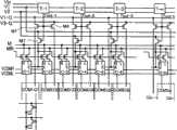
图1是表示本发明的实施例1的扫描线驱动电路的概略结构的框图。此外,本实施例与图19同样地,是驱动IPS方式的液晶显示板的扫描线(Gn)和对置电极线(COM1~COMn+1)的电路。FIG. 1 is a block diagram showing a schematic configuration of a scanning line driving circuit according to
在本实施例中是在图19所示的扫描线驱动电路重新附加了(V1-G、V2-G)的扫描线驱动用时钟信号和晶体管(M1′)的电路。In this embodiment, a scanning line driving clock signal (V1-G, V2-G) and a transistor (M1') are newly added to the scanning line driving circuit shown in FIG. 19 .
在图19所示的扫描线驱动电路中,通过给晶体管(M1)的栅极施加(Tout-0~Tout-n)的移位脉冲、给晶体管(M1)的漏极施加(V1、V2)的传送时钟信号,来驱动各级的扫描线(G0~Gn)。In the scanning line driving circuit shown in FIG. 19, by applying a shift pulse (Tout-0~Tout-n) to the gate of the transistor (M1), applying (V1, V2) to the drain of the transistor (M1) The transmission clock signal is used to drive the scanning lines (G0-Gn) of each level.
在本实施例中,通过设置新的晶体管(M1′)、并给晶体管(M1)的栅极施加(Tout-0~Tout-n)的移位脉冲、另外给晶体管(M1)的漏极施加(V1-G、V2-G)的扫描线驱动用时钟信号,来驱动各级的扫描线(G0~Gn)。In this embodiment, by setting a new transistor (M1'), applying a shift pulse (Tout-0~Tout-n) to the gate of the transistor (M1), and applying a shift pulse to the drain of the transistor (M1) Scanning line driving clock signals (V1-G, V2-G) drive the scanning lines (G0 to Gn) of each stage.
另外,(C-1~C-n+1)的对置电极扫描电路(本发明的信号线扫描电路),与图19所示的扫描线驱动电路同样地,将(V1、V2)的传送时钟信号用作对置电极扫描电路的动作信号。In addition, the counter electrode scanning circuit of (C-1 to C-n+1) (the signal line scanning circuit of the present invention), similarly to the scanning line driving circuit shown in FIG. The clock signal is used as an operation signal for the counter electrode scanning circuit.
例如,(C-1)的对置电极扫描电路,根据传送时钟信号(V1)、 交流化信号(M)、反转交流化信号(MB),确定输出H电平的公共电压(VCOMH)、或L电平的公共电压(VCOML)中的哪一个,通过输入传送时钟信号(V2)作为使能信号(E),从而给对置电极线(COM1~COM-n+1)输出H电平的公共电压(VCOMH)、或L电平的公共电压(VCOML)的任一个。For example, the counter-electrode scanning circuit of (C-1) determines the common voltage (VCOMH) outputting the H level, Either of the common voltage (VCOML) of the L level, by inputting the transfer clock signal (V2) as the enable signal (E), the H level is output to the opposite electrode line (COM1~COM-n+1) Either the common voltage (VCOMH) of the L level or the common voltage (VCOML) of the L level.
这样,在本实施例中,作为扫描线(G0~Gn)用的选择扫描电压,通过在栅极施加移位脉冲(Tout-0~Tout-n)的晶体管(M 1),输出(V1-G、V2-G)的扫描线驱动用时钟信号,另外,通过在栅极施加移位脉冲(Tout-0~Tout-n)的晶体管(M1′),给对置电极线(COM1~COMn+1)输出(V1、V2)的传送时钟信号。In this way, in this embodiment, as the selection scan voltage for the scan lines (G0-Gn), the transistor (M1) that applies the shift pulse (Tout-0-Tout-n) to the gate outputs (V1- G, V2-G) scanning line driving clock signal, in addition, through the transistor (M1') that applies the shift pulse (Tout-0~Tout-n) to the gate, to the opposite electrode line (COM1~COMn+ 1) The transfer clock signal of (V1, V2) is output.
即,在本实施例中,分离时钟信号,将(V1、V2)的传送时钟信号用于移位寄存电路(T-0~T-n)和对置电极扫描电路(C-1~C-n+1)的控制,另外,将(V1-G、V2-G)的扫描线驱动用时钟信号用于对扫描线(G0~Gn)输出扫描电压。That is, in this embodiment, the clock signals are separated, and the transfer clock signals (V1, V2) are used for the shift register circuits (T-0 to T-n) and the counter electrode scanning circuits (C-1 to C-n+ In the control of 1), the scanning line driving clock signals (V1-G, V2-G) are used to output scanning voltages to the scanning lines (G0 to Gn).
因此,在图18B、图18C的帧的黑部不进行栅极扫描(即,对扫描线输出非选择扫描电压),这在图19所示的扫描线驱动电路中是不可能的。Therefore, gate scanning (that is, non-selection scanning voltage is output to the scanning line) is not performed in the black portion of the frame shown in FIG. 18B and FIG. 18C , which is impossible in the scanning line driving circuit shown in FIG. 19 .
此外,在图1中,(T-0)的移位寄存电路,是为了给(C-1)的对置电极扫描电路输入交流化信号(M)和反转交流化信号(MB)而设置的。In addition, in FIG. 1, the shift register circuit of (T-0) is provided for inputting the alternating signal (M) and the inverted alternating signal (MB) to the opposing electrode scanning circuit of (C-1). of.
因此,在输入了启动脉冲(Vin)后,只要在输出移位脉冲(Tout-0)的时刻能够给(C-1)的对置电极扫描电路输入交流化信号(M)和反转交流化信号(MB),就不需要(T-0)的移位寄存电路和在栅极施加移位脉冲(Tout-0)的晶体管(M1′)。Therefore, after the start pulse (Vin) is input, as long as the AC signal (M) and the reverse AC signal can be input to the counter electrode scanning circuit of (C-1) at the moment of outputting the shift pulse (Tout-0), signal (MB), there is no need for a shift register circuit (T-0) and a transistor (M1') for applying a shift pulse (Tout-0) to the gate.
图2是表示图1所示的扫描线驱动电路中的部分显示驱动时的1帧内的时序图。FIG. 2 is a timing chart showing a part of display driving in one frame in the scanning line driving circuit shown in FIG. 1 .
如图2所示,不进行栅极扫描的期间(图2的Goff),(V1-G、V2-G)的扫描线驱动用时钟信号固定为L电平,因而对该期间的扫描线(在图2中,为G3、G4)输出非选择扫描电压。另外,交 流化信号(M)和反转交流化信号(MB)为帧反转驱动波形。As shown in FIG. 2, during the period when the gate scan is not performed (Goff in FIG. 2), the clock signal for driving the scanning line (V1-G, V2-G) is fixed at L level, so the scanning line (Goff) during this period is In FIG. 2, non-selection scanning voltages are output for G3, G4). In addition, the alternating signal (M) and the inverted alternating signal (MB) are frame inversion drive waveforms.
图3是表示图1所示的扫描线驱动电路中的包含通常显示驱动的部分显示驱动的5帧大小的时序图。3 is a timing chart showing five frames of partial display driving including normal display driving in the scanning line driving circuit shown in FIG. 1 .
在图3中,A为通常显示期间,该通常显示期间A如图3的G的波形所示是行反转期间。In FIG. 3 , A is a normal display period, and this normal display period A is a row inversion period as shown by the waveform of G in FIG. 3 .
B~F是部分显示期间,在(C、D)的部分2、3帧中,存在着(V1-G、V2-G)的扫描线驱动用时钟信号固定为L电平,不进行栅极扫描的期间(图3的Goff期间)。B~F are part of the display period. In the
进而,在部分显示期间(B~F),控制交流化信号(M)和反转交流化信号(MB),进行帧反转驱动。借助于该Goff期间和帧反转效果可以实现节电化。Furthermore, in the partial display periods (B to F), the alternating signal (M) and the inverted alternating signal (MB) are controlled to perform frame inversion driving. Power saving can be realized by the Goff period and the frame inversion effect.
图4是表示图1所示的扫描线驱动电路中的变形例的部分显示驱动时的1帧内的时序图。4 is a timing chart showing a partial display drive in one frame in a modified example of the scanning line driving circuit shown in FIG. 1 .
图4所示的例是使Goff期间的(V1、V2)的传送时钟信号的电压降低ΔV的例。The example shown in FIG. 4 is an example in which the voltage of the transfer clock signal during the Goff period (V1, V2) is lowered by ΔV.
通过降低(V1、V2)的传送时钟信号的电压,图1的晶体管(M1、M1′)的栅极电压降低,作为结果,晶体管的导通电阻增加。然而,由于在Goff期间,晶体管(M1)的漏极侧(供给V1的时钟信号的一侧)为L电平的电位,所以栅极电压低不存在问题。By lowering the voltage of the transfer clock signal of (V1, V2), the gate voltage of the transistor (M1, M1') of FIG. 1 is lowered, and as a result, the on-resistance of the transistor is increased. However, during the Goff period, since the drain side of the transistor (M1) (the side to which the clock signal of V1 is supplied) is at an L level potential, there is no problem that the gate voltage is low.
进而,即使晶体管(M1′)的栅极电压降低,由于对置电极扫描电路(C-1~C-n+1)的输入负载与扫描线相比非常低(通常为100∶1以上),因此由栅极电压降低而导致的晶体管的导通电阻增加也不会引起任何题。Furthermore, even if the gate voltage of the transistor (M1') is lowered, since the input load of the counter electrode scanning circuit (C-1 to C-n+1) is very low compared with the scanning line (usually 100:1 or more), Therefore, the increase in the on-resistance of the transistor due to the reduction in the gate voltage does not cause any problems.
在Goff期间,降低传送时钟信号的电压,可以适用于后述的所有实施例,通过该低电压效果,可以实现进一步的节电化。During the Goff period, lowering the voltage of the transmission clock signal can be applied to all the embodiments described later, and further power saving can be realized by this low voltage effect.
[实施例2][Example 2]
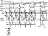
图5是表示本发明的实施例2的扫描线驱动电路的概略结构的框图。5 is a block diagram showing a schematic configuration of a scanning line driving circuit according to
相对上述实施例,本实施例是减少了移位寄存电路(T-1~ T-n)的块数、追加了晶体管(M4)的电路。Compared with the above-mentioned embodiments, this embodiment is a circuit in which the number of shift register circuits (T-1 to T-n) is reduced and a transistor (M4) is added.
如图5所示,作为移位寄存电路(T-1~T-n)的输出的移位脉冲(Tout-1~Tout-n),施加在扫描线驱动用的晶体管(M1)的栅极和新追加的晶体管(M4)的栅极。As shown in FIG. 5, the shift pulses (Tout-1~Tout-n) which are the outputs of the shift register circuits (T-1~T-n) are applied to the gate and the new transistor (M1) for driving the scanning line. Gate of the additional transistor (M4).
在漏极施加(V1-G)的扫描线驱动用时钟信号的晶体管(M1),驱动扫描线(例如,G1扫描线)(即,对扫描线(G1)输出选择扫描电压),在漏极施加(V2-G)的扫描线驱动用时钟信号的晶体管(M4)驱动扫描线(例如,G2扫描线)。Transistor (M1) that applies (V1-G) scanning line driving clock signal to the drain to drive the scanning line (for example, G1 scanning line) (that is, output selection scanning voltage to the scanning line (G1)), and A transistor ( M4 ) to which a scanning line driving clock signal of ( V2 - G ) is applied drives a scanning line (for example, G2 scanning line).
即,在本实施例中,移位寄存电路(T-1~T-n),对各级驱动2条扫描线。因此,移位寄存电路(T-1~T-n)的传送周期为栅极驱动周期的一半。That is, in this embodiment, the shift register circuits (T-1 to T-n) drive two scanning lines for each stage. Therefore, the transfer period of the shift register circuits (T-1˜T-n) is half of the gate driving period.
这意味着(V1、V2)的传送时钟信号的频率为(V1-G、V2-G)的栅极驱动用的扫描线驱动用时钟信号的频率的1/2,因此,可以降低(V1、V2)的传送时钟信号的频率,实现耗电量的降低。This means that the frequency of the transmission clock signal of (V1, V2) is 1/2 of the frequency of the scanning line driving clock signal for gate driving of (V1-G, V2-G), therefore, it is possible to reduce the frequency of (V1, V2). V2) transmits the frequency of the clock signal to reduce power consumption.
另外,在栅极施加移位脉冲(Tout-1~Tout-n)的晶体管(M1′),将施加在漏极的(V1、V2)的传送时钟信号输入到对置电极扫描电路(C-1~C-2n)。In addition, the transistor (M1') applying the shift pulse (Tout-1 to Tout-n) to the gate inputs the transfer clock signal (V1, V2) applied to the drain to the counter electrode scanning circuit (C- 1~C-2n).
该信号,用于H电平的公共电压(VCOMH)或L电平的公共电压(VCOML)的确定、以及用作使能信号。This signal is used to determine the common voltage at the H level (VCOMH) or the common voltage at the L level (VCOML), and is used as an enable signal.
对邻接的2级的对置电极扫描电路,分别经由相同的晶体管(M1′),输入(V1、V2)的传送时钟信号,所以邻接的2级的对置电极扫描电路选择相同极性的公共电压,并同时进行输出。Since the transfer clock signals (V1, V2) are input to the adjacent two-stage opposing electrode scanning circuits via the same transistor (M1'), the adjacent two-stage opposing electrode scanning circuits select common voltage, and output simultaneously.
因此,不能按每1行反转施加在对置电极(ITO2)的电压的极性,通常显示期间按每2个水平期间切换交流化信号(M)和反转交流化信号(MB),进行2行反转驱动,部分显示期间按每1个垂直期间切换,进行帧反转。Therefore, the polarity of the voltage applied to the counter electrode (ITO2) cannot be reversed every row, and the alternating signal (M) and the reversed alternating signal (MB) are switched between the alternating signal (M) and the reversed alternating signal (MB) every two horizontal periods during the normal display period. 2-line inversion drive, and the partial display period is switched every vertical period to perform frame inversion.
图6是表示图5所示的扫描线驱动电路中的部分显示驱动时的1帧内的时序图。FIG. 6 is a timing chart showing a part of display driving in one frame in the scanning line driving circuit shown in FIG. 5 .
与上述实施例同样地,不进行栅极扫描的期间(Goff期间), (V1-G、V2-G)的扫描线驱动用时钟信号固定为L电平。另外,交流化信号(M)和反转交流化信号(MB)为进行帧反转驱动的波形。Similar to the above-mentioned embodiment, during the period when gate scanning is not performed (Goff period), the scanning line driving clock signal (V1-G, V2-G) is fixed at L level. In addition, the alternating signal (M) and the inverted alternating signal (MB) are waveforms for performing frame inversion driving.
图7是表示图5所示的扫描线驱动电路中的包含通常显示驱动的部分显示驱动5帧大小的时序图。该图7,除了(V1、V2)的传送时钟信号、交流化信号(M)和反转交流化信号(MB),以(V1-G、V2-G)的扫描线驱动用时钟信号的一半的频率进行动作以外,其余的与上述图3相同。7 is a timing chart showing five frames of partial display driving including normal display driving in the scanning line driving circuit shown in FIG. 5 . In this figure 7, in addition to the transmission clock signal (V1, V2), the AC signal (M) and the inverted AC signal (MB), half of the clock signal for scanning line driving (V1-G, V2-G) Except for the operation at the frequency, the rest is the same as in Fig. 3 above.
即,在图7中,A为通常显示期间,该期间如图7的G的波形所示,是行反转期间(2行反转)。B~F是部分显示期间,在(C、D)的部分2、3帧中,存在着(V1-G、V2-G)的扫描线驱动用时钟信号固定为L电平,不进行栅极扫描的期间(即,对扫描线输出非选择扫描电压的期间;图7的Goff期间)。That is, in FIG. 7 , A is a normal display period, and this period is a line inversion period (two-line inversion) as shown by the waveform of G in FIG. 7 . B~F are part of the display period. In the
此外,在本实施例中,示出了对1级的移位寄存电路(T-1~T-n)驱动2条扫描线的例子,但通过使(V1、V2)的传送时钟信号的频率进一步低周期化,可以将扫描线驱动条数增加到任意多条。因此,可以进一步降低耗电量。In addition, in this embodiment, an example of driving two scanning lines for one stage of shift register circuits (T-1 to T-n) is shown, but by making the frequency of the transmission clock signal of (V1, V2) lower Periodization, the number of scanning line drivers can be increased to any number. Therefore, power consumption can be further reduced.
[实施例3][Example 3]
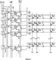
图8是表示本发明的实施例3的扫描线驱动电路的概略结构的框图。8 is a block diagram showing a schematic configuration of a scanning line driving circuit according to
本实施例是针对上述实施例新追加了(V1-C、V2-C)的公共电极驱动用时钟信号(本发明的信号线驱动用时钟信号)和晶体管(M4′)的电路结构。栅极驱动方法与上述实施例的相同。This embodiment is a circuit configuration in which a common electrode driving clock signal (signal line driving clock signal of the present invention) and a transistor (M4') are newly added (V1-C, V2-C) to the above-mentioned embodiment. The gate driving method is the same as that of the above-mentioned embodiment.
另一方面,在栅极施加移位脉冲(Tout-1~Tout-n)的晶体管(M1′),将施加在漏极的(V1-C)的公共控制时钟信号用于确保每隔一个的对置电极扫描电路(C-2、C-4、C-6、...)的公共电压的极性、以及用作每隔一个的对置电极扫描电路(C-1、C-3、C-5、...)的使能信号。On the other hand, the transistors (M1') to which shift pulses (Tout-1~Tout-n) are applied to the gates use the common control clock signal (V1-C) applied to the drains to ensure that every other The polarity of the common voltage of the counter electrode scanning circuits (C-2, C-4, C-6, ...), and the polarity of the common voltage used as every other counter electrode scanning circuit (C-1, C-3, C-5, ...) enable signal.
另外,在栅极施加移位脉冲(Tout-1~Tout-n)的晶体管(M4′), 将施加在漏极的(V2-C)的公共控制时钟信号用于确保每隔一个对置电极扫描电路(C-1、C-3、C-5、...)的公共电压的极性、以及用作每隔一个的对置电极扫描电路(C-2、C-4、C-6、...)的使能信号。In addition, the transistor (M4') applying the shift pulse (Tout-1~Tout-n) to the gate uses the common control clock signal (V2-C) applied to the drain to ensure that every other opposite electrode The polarity of the common voltage of the scanning circuits (C-1, C-3, C-5, ...), and the counter electrode used as every other scanning circuit (C-2, C-4, C-6 ,...) enable signal.
由此,输入到对置电极扫描电路(C-1~C-2n)的信号,在对置电极扫描电路的各级中是独立的,按每1级独立地进行H电平的公共电压(VCOMH)或L电平的公共电压(VCOML)的确定和输出。Accordingly, the signals input to the counter electrode scanning circuits (C-1 to C-2n) are independent in each stage of the counter electrode scanning circuit, and the H level common voltage ( VCOMH) or L-level common voltage (VCOML) determination and output.
因此,交流化方式与上述实施例的2行反转驱动不同,通常显示期间能够进行1行反转驱动,部分显示期间能够进行帧反转驱动,与上述实施例1相同。由此,能够避免在2行反转驱动中所担心的画质恶化。Therefore, the alternating method is different from the 2-line inversion driving in the above-mentioned embodiment. One-line inversion driving can be performed during the normal display period, and the frame inversion driving can be performed during the partial display period, which is the same as the above-mentioned first embodiment. As a result, it is possible to avoid deterioration of the image quality which is a concern in the 2-line inversion driving.
图9是表示图8所示的扫描线驱动电路中的部分显示驱动时的1帧内的时序图。FIG. 9 is a timing chart showing partial display driving in one frame in the scanning line driving circuit shown in FIG. 8 .
与图6所示的时序图不同的是给对置电极(COMn)施加的公共电压按每1级依次输出。The difference from the timing chart shown in FIG. 6 is that the common voltage applied to the counter electrode (COMn) is sequentially output every step.
(V1-C、V2-C)的公共控制时钟信号,是以与(V1-G、V2-G)的扫描线驱动用时钟信号相同的频率进行驱动的信号,在不进行栅极扫描的期间(Goff期间)也持续输出。The common control clock signal of (V1-C, V2-C) is a signal that is driven at the same frequency as the scanning line driving clock signal of (V1-G, V2-G). During the period when gate scanning is not performed (during Goff) also keeps outputting.
图10是表示图8所示的扫描线驱动电路中的包含通常显示驱动的部分显示驱动5帧大小的时序图。FIG. 10 is a timing chart showing five frames of partial display driving including normal display driving in the scanning line driving circuit shown in FIG. 8 .
在图10中,A为通常显示期间,该期间是行反转期间(1行反转)。B~F是部分显示期间,在(C、D)的部分2、3帧中,存在着(V1-G、V2-G)的扫描线驱动用时钟信号固定为L电平,不进行栅极扫描的期间(即,图10的Goff期间)。In FIG. 10, A is a normal display period, and this period is a row inversion period (one row inversion). B~F are part of the display period. In the
图10中,在通常显示期间(A),按每1个水平期间切换交流化信号(M)和反转交流化信号(MB),进行行反转,在部分显示期间(B~F),按每1个垂直期间(帧)切换交流化信号(M)和反转交流化信号(MB),进行帧反转驱动。由此,可以通过时 分驱动实现低电力化,同时可以避免画质恶化。In FIG. 10, in the normal display period (A), the alternating signal (M) and the inverted alternating signal (MB) are switched every horizontal period to perform line inversion, and in the partial display period (B to F), The frame inversion driving is performed by switching the alternating signal (M) and the inverted alternating signal (MB) every one vertical period (frame). As a result, power consumption can be reduced by time-division driving, while image quality degradation can be avoided.
[实施例4][Example 4]
图11是表示本发明的实施例4的扫描线驱动电路的概略结构的框图。11 is a block diagram showing a schematic configuration of a scanning line driving circuit according to
是对上述实施例2新追加了(SEL、SELB)的选择信号、(MS、MSB)的第2交流化信号、以及晶体管(M5、M5′、M6、M6′)的电路。This is a circuit in which a selection signal of (SEL, SELB), a second AC signal of (MS, MSB), and transistors (M5, M5', M6, M6') are newly added to the above-mentioned second embodiment.
栅极驱动方法,与上述实施例2相同,但在显示时和非显示时,给对置电极扫描电路(C-1~C-2n)输入不同的使能信号这一点上,与上述实施例2不同。The gate driving method is the same as that of the above-mentioned
显示时和非显示时的输入切换,由新追加的选择信号(SEL、SELB)进行。Input switching between display and non-display is performed by newly added selection signals (SEL, SELB).
进行栅极扫描的期间,例如,在通常显示时和部分显示时的显示部中,SEL的选择信号固定为H电平、SELB的选择信号固定为L电平。由此,晶体管(M5、M5′)导通、晶体管(M6、M6′)截止。During gate scanning, for example, in the display section during normal display and partial display, the selection signal of SEL is fixed at H level and the selection signal of SELB is fixed at L level. As a result, the transistors (M5, M5') are turned on and the transistors (M6, M6') are turned off.
当晶体管(M5)导通时,经晶体管(M1),(V1-G)的扫描线驱动用时钟信号输入到每隔一个的对置电极扫描电路(C-1、C-3、C-5、...),成为(E-1、E-3、E-5、...)的使能信号。When the transistor (M5) was turned on, through the transistor (M1), the scanning line driving clock signal of (V1-G) was input to every other opposite electrode scanning circuit (C-1, C-3, C-5 ,...), become the enable signal of (E-1, E-3, E-5,...).
同样地,当晶体管(M5′)导通时,经晶体管(M4),(V2-G)的扫描线驱动用时钟信号输入到每隔一个的对置电极扫描电路(C-2、C-4、C-6、...),成为(E-2、E-4、E-6、...)的使能信号。Similarly, when the transistor (M5') is turned on, the scanning line driving clock signal of the transistor (M4) and (V2-G) is input to every other opposing electrode scanning circuit (C-2, C-4 , C-6, ...), become the enable signal of (E-2, E-4, E-6, ...).
另外,栅极扫描按每1级依次进行,因此从对置电极扫描电路(C-1~C-2n)给对置电极(ITO2)输出的公共电压的输出动作也按每1级依次进行。In addition, since the gate scanning is sequentially performed every step, the output operation of the common voltage output from the counter electrode scanning circuits (C-1 to C-2n) to the counter electrode (ITO2) is also sequentially performed every step.
另一方面,在部分显示期间,不进行栅极扫描的期间(后述的图12的Goff期间),将SEL的选择信号固定为L电平、将SELB的选择信号固定为H电平,因而晶体管(M5、M5′)截止、晶体 管(M6、M6′)导通。On the other hand, in the partial display period, when the gate scan is not performed (the Goff period in FIG. 12 described later), the selection signal of SEL is fixed at L level, and the selection signal of SELB is fixed at H level. Transistors (M5, M5') are turned off, and transistors (M6, M6') are turned on.
给晶体管(M6、M6′)的漏极施加由移位寄存电路(T-1~T-n)输出的移位脉冲(Tout-1~Tout-n)。因此,移位脉冲(Tout-1~Tout-n)成为对置电极扫描电路(C-1~C-2n)的(E-1~E-2n)的使能信号。The shift pulses (Tout-1 to Tout-n) output from the shift register circuits (T-1 to T-n) are applied to the drains of the transistors (M6, M6'). Therefore, the shift pulses (Tout-1 to Tout-n) serve as enable signals of (E-1 to E-2n) of the counter electrode scanning circuits (C-1 to C-2n).
在这种情况下,对邻接的2级的对置电极扫描电路,输入相同的移位脉冲作为使能信号,因而来自邻接的2级的对置电极扫描电路的输出动作同时进行。因此,成为2行同时输出,但是,部分显示期间是不对子像素进行写入的期间,因而由2行同时输出引起的画质降低在显示上不存在问题。In this case, since the same shift pulse is input as an enable signal to two adjacent counter electrode scanning circuits, the output operations from the two adjacent counter electrode scanning circuits are performed simultaneously. Therefore, two lines are simultaneously output, but since a part of the display period is a period in which subpixels are not written, there is no problem in terms of image quality degradation due to two line simultaneous output.
这样,在本实施例中,作为输入到对置电极扫描电路(C-1~C-2n)的使能信号,在进行栅极扫描的期间,使用扫描线驱动用时钟信号(V1-G、V2-G),在不进行栅极扫描的期间,使用移位脉冲(Tout-1~Tout-n),因此,可以不使用公共控制时钟信号(V1-C、V2-C)地驱动对置电极扫描电路,而不会使显示部的画质恶化。Thus, in this embodiment, as the enable signal input to the counter electrode scanning circuits (C-1 to C-2n), the scanning line driving clock signal (V1-G, V2-G), during the period when gate scanning is not performed, shift pulses (Tout-1~Tout-n) are used, therefore, the opposite can be driven without using common control clock signals (V1-C, V2-C) Electrode scanning circuit without deteriorating the image quality of the display part.
此外,对H电平的公共电压(VCOMH)、或L电平的公共电压(VCOML)的确定,用移位脉冲(Tout-1~Tout-n)2行同时地进行确定。In addition, determination of the common voltage (VCOMH) at the H level or the common voltage (VCOML) at the L level is determined simultaneously by two shift pulses (Tout-1 to Tout-n).
因此,仅交流化信号(M)和反转交流化信号(MB),不能实现每1行的公共极性反转,需要新追加交流化信号(MS)和反转交流化信号(MSB)。Therefore, only the alternating signal (M) and the inverted alternating signal (MB) cannot achieve the common polarity inversion for each row, and it is necessary to newly add the alternating signal (MS) and the inverted alternating signal (MSB).
第1交流化信号(M)和第1反转交流化信号(MB),确定对置电极扫描电路(C-1、C-3、...)的极性,第2交流化信号(MS)和第2反转交流化信号(MSB),确定对置电极扫描电路(C-2、C-4、...)的极性。The first AC signal (M) and the first inverted AC signal (MB) determine the polarity of the counter electrode scanning circuit (C-1, C-3, ...), the second AC signal (MS ) and the second inverted AC signal (MSB), to determine the polarity of the counter electrode scanning circuit (C-2, C-4, ...).
第1交流化信号(M)和第1反转交流化信号(MB)、以及第2交流化信号(MS)和第2反转交流化信号(MSB),分别为相位相反的信号。The first AC signal (M) and the first inverted AC signal (MB), and the second AC signal (MS) and the second inverted AC signal (MSB) are signals with opposite phases, respectively.
进而,如果第1交流化信号(M)和第2交流化信号(MS)为同相位,则邻接的2级的对置电极扫描电路(例如,C-1、C-2)为同极性。Furthermore, if the first alternating signal (M) and the second alternating signal (MS) are in the same phase, the adjacent two-stage counter electrode scanning circuits (for example, C-1, C-2) have the same polarity .
如果第1交流化信号(M)和第2交流化信号(MS)的相位相反,则邻接的2级的对置电极扫描电路(例如,C-1、C-2)的极性相反。If the phases of the first alternating signal (M) and the second alternating signal (MS) are opposite, the polarities of the two adjacent counter electrode scanning circuits (for example, C-1, C-2) are opposite.
因此,通过控制第1交流化信号(M)、第1反转交流化信号(MB)、第2交流化信号(MS)和第2反转交流化信号(MSB),可以任意地控制帧反转、行反转。Therefore, by controlling the first AC signal (M), the first inverted AC signal (MB), the second AC signal (MS) and the second inverted AC signal (MSB), the frame inversion can be arbitrarily controlled. Turn, row reverse.
图12是表示图11所示的扫描线驱动电路中的部分显示驱动时的1帧内的时序图。FIG. 12 is a timing chart showing a part of display driving in one frame in the scanning line driving circuit shown in FIG. 11 .
如图12所示,进行栅极扫描的期间,输出(V1-G、V2-G)的扫描线驱动用时钟信号,选择信号(SEL)固定为H电平、选择信号(SELB)固定为L电平。As shown in FIG. 12, during the gate scanning period, the clock signal for driving the scanning line (V1-G, V2-G) is output, the selection signal (SEL) is fixed at H level, and the selection signal (SELB) is fixed at L level. level.
不进行栅极扫描的期间(图12的Goff期间),(V1-G、V2-G)的扫描线驱动用时钟信号固定为L电平。该期间,选择信号(SEL)固定为L电平、选择信号(SELB)固定为H电平。During the period when gate scanning is not performed (the Goff period in FIG. 12 ), the scanning line driving clock signals (V1-G, V2-G) are fixed at L level. During this period, the selection signal (SEL) is fixed at L level, and the selection signal (SELB) is fixed at H level.
第1交流化信号(M)和第2交流化信号(MS)、以及第1反转交流化信号(MB)和第2反转交流化信号(MSB),为相互以同极性固定1个垂直期间(帧),帧反转驱动的波形。The first AC signal (M) and the second AC signal (MS), as well as the first inverted AC signal (MB) and the second inverted AC signal (MSB), are fixed at the same polarity as each other. In the vertical period (frame), the waveform of the frame inversion drive.
图13是表示图11所示的扫描线驱动电路中的包含通常显示驱动的部分显示驱动5帧大小的时序图。FIG. 13 is a timing chart showing five frames of partial display driving including normal display driving in the scanning line driving circuit shown in FIG. 11 .
在图13中,A为通常显示期间,该期间是行反转期间(1行反转)。B~F是部分显示期间,在(C、D)的部分2、3帧中,存在着不进行栅极扫描的期间(即,图13的Goff期间)。In FIG. 13, A is a normal display period, and this period is a row inversion period (one row inversion). B to F are partial display periods, and in the second and third frames of (C, D), there is a period in which gate scanning is not performed (that is, the Goff period in FIG. 13 ).
第1交流化信号(M)和第2交流化信号(MS)、以及第1反转交流化信号(MB)和第2反转交流化信号(MSB),在通常显示期间(A),为实现行反转,相互间相位相反,在部分显示期间(B~F),为实现帧反转,相互间相位相同。The first AC signal (M) and the second AC signal (MS), and the first inverted AC signal (MB) and the second inverted AC signal (MSB), during the normal display period (A), are To achieve line inversion, the phases are opposite to each other. During the partial display period (B-F), to achieve frame inversion, the phases are the same.
这样,在本实施例中,可以不使用公共控制时钟信号(V1-C、V2-C)地进行部分显示,而不会对显示部的画质产生影响,因而削减了因公共控制时钟信号(V1-C、V2-C)而增加的耗电量部分,可以降低耗电量。In this way, in this embodiment, partial display can be performed without using the common control clock signal (V1-C, V2-C), without affecting the image quality of the display part, thus reducing the frequency caused by the common control clock signal (V1-C, V2-C). V1-C, V2-C) and the increased power consumption can reduce power consumption.
[实施例5][Example 5]
作为液晶显示装置的驱动方法,已知有独立电容耦合(Charge-Coupling:电荷耦合)驱动方法(例如,参照专利文献2)。As a driving method of a liquid crystal display device, an independent capacitive coupling (Charge-Coupling: Charge-Coupling) driving method is known (for example, refer to Patent Document 2).
图14是表示独立电容耦合(Charge-Coupling:电荷耦合)驱动液晶显示板的1个子像素的等效电路的电路图。14 is a circuit diagram showing an equivalent circuit of one sub-pixel of a liquid crystal display panel driven by independent capacitive coupling (Charge-Coupling).
在图14中,Gn是扫描线,Sn是视频线,GEn是补偿线,CLc是液晶电容,Cst是存储电容,TFT是薄膜晶体管,ITO1是像素电极,ITO2是对置电极。此外,在图14中,使像素电极(ITO1)和对置电极(ITO2)隔着液晶相对地设置,因此,沿着与基板正交的方向对液晶施加电场。In FIG. 14, Gn is a scanning line, Sn is a video line, GEn is a compensation line, CLc is a liquid crystal capacitor, Cst is a storage capacitor, TFT is a thin film transistor, ITO1 is a pixel electrode, and ITO2 is an opposite electrode. In addition, in FIG. 14 , since the pixel electrode ( ITO1 ) and the counter electrode ( ITO2 ) are provided facing each other across the liquid crystal, an electric field is applied to the liquid crystal in a direction perpendicular to the substrate.
在独立电容耦合(Charge-Coupling:电荷耦合)驱动方法中,向扫描线(Gn)施加扫描电压,使薄膜晶体管(TFT)导通,并在1个显示期间内从视频线(Sn)对像素电极(ITO1)施加来自视频线(Sn)的视频电压。之后,使薄膜晶体管(TFT)截止,向补偿线(GEn)施加补偿电压。In the independent capacitive coupling (Charge-Coupling: charge-coupled) driving method, a scanning voltage is applied to the scanning line (Gn) to turn on the thin-film transistor (TFT), and the pixel is connected to the pixel from the video line (Sn) within one display period. The electrode (ITO1) applies the video voltage from the video line (Sn). Thereafter, the thin film transistor (TFT) is turned off, and a compensation voltage is applied to the compensation line (GEn).
这样,在独立电容耦合(Charge-Coupling:电荷耦合)驱动方法中,写入各子像素的电压,由从视频线(Sn)施加的视频电压和从补偿线(GEn)施加的补偿电压决定。Thus, in the independent capacitive coupling (Charge-Coupling) driving method, the voltage written to each sub-pixel is determined by the video voltage applied from the video line (Sn) and the compensation voltage applied from the compensation line (GEn).
图15是表示驱动现有的独立电容耦合(Charge-Coupling:电荷耦合)驱动液晶显示板的扫描线驱动电路的概略结构的框图。图16是表示图15所示的扫描线驱动电路的时序图。15 is a block diagram showing a schematic configuration of a scanning line drive circuit for driving a conventional independent capacitive coupling (Charge-Coupling: charge-coupled) drive liquid crystal display panel. FIG. 16 is a timing chart showing the scanning line driving circuit shown in FIG. 15 .
在图15中,例如,(C-2)的对置电极扫描电路,根据经导通的晶体管(M2、M3)而输入的交流化信号(M)和反转交流化信号(MB),确定输出H电平的补偿电压(VCH)、或L电平的补偿电压(VCL)中的哪一个,并输入传送时钟信号(V1)作为 使能信号(E),从而对前级的补偿线(GE1)输出H电平或L电平的补偿电压,其中,上述晶体管是由传送时钟信号(V2)而成为导通的。In FIG. 15, for example, the opposing electrode scanning circuit of (C-2) determines the AC signal (M) and the inverted AC signal (MB) inputted through the turned-on transistors (M2, M3). Which one of the H-level compensation voltage (VCH) or the L-level compensation voltage (VCL) is output, and the transmission clock signal (V1) is input as the enable signal (E), so that the compensation line of the previous stage ( GE1) outputs an H-level or L-level compensation voltage, wherein the above-mentioned transistor is turned on by transmitting a clock signal (V2).
本发明也可以适用于该独立电容耦合(Charge-Coupling:电荷耦合)驱动液晶显示板。在这种情况下,在上述的各实施例中,只需从(C-1~C-n+1)的各对置电极扫描电路向前级的补偿线输出H电平或L电平的补偿电压即可。The present invention can also be applied to this independent capacitive coupling (Charge-Coupling: charge-coupled) drive liquid crystal display panel. In this case, in each of the above-mentioned embodiments, it is only necessary to output H-level or L-level signals from the counter-electrode scanning circuits (C-1 to C-n+1) to the compensation line of the previous stage. compensation voltage.
此外,在图15中,(T-0)的移位寄存电路和(C-1)的对置电极扫描电路与显示板的动作无关,因此也可以省略(T-0)的移位寄存电路、(C-1)的对置电极扫描电路、以及将这2个电路的输出作为输入的晶体管(M1、M2、M3)。In addition, in FIG. 15, the shift register circuit of (T-0) and the counter electrode scanning circuit of (C-1) have nothing to do with the operation of the display panel, so the shift register circuit of (T-0) can also be omitted. , the counter electrode scanning circuit of (C-1), and the transistors (M1, M2, M3) that receive the outputs of these two circuits as inputs.
以上,根据上述实施例具体地说明了本发明人提出的发明,本发明当然不限于上述实施例,在不脱离其主旨的范围内可以进行各种变更。As mentioned above, although the invention proposed by this inventor was concretely demonstrated based on the said Example, this invention is of course not limited to the said Example, Various changes are possible in the range which does not deviate from the summary.
Claims (27)
Applications Claiming Priority (2)
| Application Number | Priority Date | Filing Date | Title |
|---|---|---|---|
| JP359799/2005 | 2005-12-14 | ||
| JP2005359799AJP4902185B2 (en) | 2005-12-14 | 2005-12-14 | Display device |
Publications (2)
| Publication Number | Publication Date |
|---|---|
| CN1983379A CN1983379A (en) | 2007-06-20 |
| CN1983379Btrue CN1983379B (en) | 2010-12-15 |
Family
ID=38138784
Family Applications (1)
| Application Number | Title | Priority Date | Filing Date |
|---|---|---|---|
| CN2006101670237AActiveCN1983379B (en) | 2005-12-14 | 2006-12-13 | display device |
Country Status (3)
| Country | Link |
|---|---|
| US (1) | US20070132703A1 (en) |
| JP (1) | JP4902185B2 (en) |
| CN (1) | CN1983379B (en) |
Families Citing this family (10)
| Publication number | Priority date | Publication date | Assignee | Title |
|---|---|---|---|---|
| KR101219043B1 (en)* | 2006-01-26 | 2013-01-07 | 삼성디스플레이 주식회사 | Display device and driving apparatus thereof |
| JP5312758B2 (en)* | 2007-06-13 | 2013-10-09 | 株式会社ジャパンディスプレイ | Display device |
| JP4455629B2 (en)* | 2007-08-22 | 2010-04-21 | 統▲宝▼光電股▲分▼有限公司 | Driving method of active matrix type liquid crystal display device |
| JP5193628B2 (en)* | 2008-03-05 | 2013-05-08 | 株式会社ジャパンディスプレイイースト | Display device |
| KR101106141B1 (en)* | 2010-09-17 | 2012-01-20 | 이성호 | Dot inversion type liquid crystal panel driving method and device |
| TWI524324B (en)* | 2014-01-28 | 2016-03-01 | 友達光電股份有限公司 | Liquid crystal display |
| KR102522535B1 (en)* | 2017-12-11 | 2023-04-17 | 엘지디스플레이 주식회사 | Gate shift register and organic light emitting display device including the same |
| KR102743732B1 (en)* | 2019-04-12 | 2024-12-19 | 삼성디스플레이 주식회사 | Scan driver and display device |
| CN112735315B (en)* | 2020-12-31 | 2024-04-02 | 厦门天马微电子有限公司 | Display panel and display device |
| KR102841501B1 (en)* | 2021-04-12 | 2025-08-05 | 삼성디스플레이 주식회사 | Electronic device and operating method of the same |
Citations (2)
| Publication number | Priority date | Publication date | Assignee | Title |
|---|---|---|---|---|
| CN1577021A (en)* | 2003-06-27 | 2005-02-09 | 三洋电机株式会社 | Display device |
| CN1577024A (en)* | 2003-07-18 | 2005-02-09 | 株式会社半导体能源研究所 | Display device and electronic apparatus |
Family Cites Families (5)
| Publication number | Priority date | Publication date | Assignee | Title |
|---|---|---|---|---|
| JP2001174784A (en)* | 1999-12-16 | 2001-06-29 | Hitachi Ltd | Liquid crystal display |
| JP3498033B2 (en)* | 2000-02-28 | 2004-02-16 | Nec液晶テクノロジー株式会社 | Display device, portable electronic device, and method of driving display device |
| JP3743503B2 (en)* | 2001-05-24 | 2006-02-08 | セイコーエプソン株式会社 | Scan driving circuit, display device, electro-optical device, and scan driving method |
| JP4360930B2 (en)* | 2004-02-17 | 2009-11-11 | 三菱電機株式会社 | Image display device |
| JP2005266178A (en)* | 2004-03-17 | 2005-09-29 | Sharp Corp | Display device drive device, display device, and display device drive method |
- 2005
- 2005-12-14JPJP2005359799Apatent/JP4902185B2/enactiveActive
- 2006
- 2006-12-13CNCN2006101670237Apatent/CN1983379B/enactiveActive
- 2006-12-13USUS11/637,723patent/US20070132703A1/ennot_activeAbandoned
Patent Citations (2)
| Publication number | Priority date | Publication date | Assignee | Title |
|---|---|---|---|---|
| CN1577021A (en)* | 2003-06-27 | 2005-02-09 | 三洋电机株式会社 | Display device |
| CN1577024A (en)* | 2003-07-18 | 2005-02-09 | 株式会社半导体能源研究所 | Display device and electronic apparatus |
Also Published As
| Publication number | Publication date |
|---|---|
| JP4902185B2 (en) | 2012-03-21 |
| US20070132703A1 (en) | 2007-06-14 |
| CN1983379A (en) | 2007-06-20 |
| JP2007163824A (en) | 2007-06-28 |
Similar Documents
| Publication | Publication Date | Title |
|---|---|---|
| CN1983379B (en) | display device | |
| US7710377B2 (en) | LCD panel including gate drivers | |
| TW594645B (en) | Liquid crystal display device having an improved precharge circuit and method of driving same | |
| KR101322002B1 (en) | Liquid Crystal Display | |
| CN100399406C (en) | Operation unit of liquid crystal display panel and operation method thereof | |
| US8581823B2 (en) | Liquid crystal display device and driving method thereof | |
| US20040183768A1 (en) | Liquid crystal display device and method for driving the same | |
| US20030006997A1 (en) | Image display device | |
| JP2006524365A (en) | Display system with frame buffer and power saving sequence | |
| KR100365500B1 (en) | Method of Driving Liquid Crystal Panel in Dot Inversion and Apparatus thereof | |
| KR20060021055A (en) | Liquid crystal display device, drive device and method for liquid crystal display device | |
| CN103280205A (en) | Display device, timing controller and image display method | |
| US7777737B2 (en) | Active matrix type liquid crystal display device | |
| JP2010085949A (en) | Liquid crystal display | |
| US20020135574A1 (en) | Driving method for flat-panel display device | |
| JP2001166741A (en) | Semiconductor integrated circuit device and liquid crystal display device | |
| JP3055620B2 (en) | Liquid crystal display device and driving method thereof | |
| US20110169790A1 (en) | Display driving circuit, display device, and display driving method | |
| KR20070068984A (en) | Driving apparatus and method of liquid crystal display device | |
| KR101174162B1 (en) | LCD Display | |
| JP5226115B2 (en) | Display device | |
| JP2007140192A (en) | Active matrix type liquid crystal display device | |
| KR100909048B1 (en) | LCD and its driving method | |
| KR100864975B1 (en) | Driving device and driving method of liquid crystal display | |
| JP2000075263A (en) | Driving circuit for active matrix type liquid crystal display device |
Legal Events
| Date | Code | Title | Description |
|---|---|---|---|
| C06 | Publication | ||
| PB01 | Publication | ||
| C10 | Entry into substantive examination | ||
| SE01 | Entry into force of request for substantive examination | ||
| C14 | Grant of patent or utility model | ||
| GR01 | Patent grant | ||
| C56 | Change in the name or address of the patentee | ||
| CP01 | Change in the name or title of a patent holder | Address after:Chiba County, Japan Co-patentee after:Panasonic Liquid Crystal Display Co.,Ltd. Patentee after:Hitachi Displays, Ltd. Address before:Chiba County, Japan Co-patentee before:IPS pioneer support society Patentee before:Hitachi Displays, Ltd. Address after:Chiba County, Japan Co-patentee after:IPS Pioneer Support Society Patentee after:Hitachi Displays, Ltd. Address before:Chiba County, Japan Patentee before:Hitachi Displays, Ltd. | |
| C56 | Change in the name or address of the patentee | Owner name:APAN DISPLAY EAST, INC. Free format text:FORMER NAME: HITACHI DISPLAY CO., LTD. Owner name:JAPAN DISPLAY, INC. Free format text:FORMER NAME: APAN DISPLAY EAST, INC. | |
| CP01 | Change in the name or title of a patent holder | Address after:Chiba County, Japan Patentee after:Japan Display East Inc. Patentee after:Panasonic Liquid Crystal Display Co.,Ltd. Address before:Chiba County, Japan Patentee before:Hitachi Displays, Ltd. Patentee before:Panasonic Liquid Crystal Display Co.,Ltd. | |
| CP03 | Change of name, title or address | Address after:Tokyo port xixinqiao Japan three chome 7 No. 1 Patentee after:JAPAN DISPLAY Inc. Patentee after:Panasonic Liquid Crystal Display Co.,Ltd. Address before:Chiba County, Japan Patentee before:Japan Display East Inc. Patentee before:Panasonic Liquid Crystal Display Co.,Ltd. | |
| EE01 | Entry into force of recordation of patent licensing contract | Application publication date:20070620 Assignee:BOE TECHNOLOGY GROUP Co.,Ltd. Assignor:JAPAN DISPLAY Inc.|Panasonic Liquid Crystal Display Co.,Ltd. Contract record no.:2013990000688 Denomination of invention:Image display Granted publication date:20101215 License type:Common License Record date:20131016 | |
| LICC | Enforcement, change and cancellation of record of contracts on the licence for exploitation of a patent or utility model | ||
| TR01 | Transfer of patent right | ||
| TR01 | Transfer of patent right | Effective date of registration:20231213 Address after:Tokyo, Japan Patentee after:JAPAN DISPLAY Inc. Patentee after:PANASONIC INTELLECTUAL PROPERTY CORPORATION OF AMERICA Address before:Tokyo port xixinqiao Japan three chome 7 No. 1 Patentee before:JAPAN DISPLAY Inc. Patentee before:Panasonic Liquid Crystal Display Co.,Ltd. | |
| TR01 | Transfer of patent right | ||
| TR01 | Transfer of patent right | Effective date of registration:20250724 Address after:Tokyo, Japan Patentee after:MAGNO SEISHIN Co., Ltd. Country or region after:Japan Patentee after:PANASONIC INTELLECTUAL PROPERTY CORPORATION OF AMERICA Country or region after:U.S.A. Address before:Tokyo, Japan Patentee before:JAPAN DISPLAY Inc. Country or region before:Japan Patentee before:PANASONIC INTELLECTUAL PROPERTY CORPORATION OF AMERICA Country or region before:U.S.A. |