CN1981232B - Method for manufacturing ophthalmic lens and optical element suitable for carrying out said method - Google Patents
Method for manufacturing ophthalmic lens and optical element suitable for carrying out said methodDownload PDFInfo
- Publication number
- CN1981232B CN1981232BCN2005800226149ACN200580022614ACN1981232BCN 1981232 BCN1981232 BCN 1981232BCN 2005800226149 ACN2005800226149 ACN 2005800226149ACN 200580022614 ACN200580022614 ACN 200580022614ACN 1981232 BCN1981232 BCN 1981232B
- Authority
- CN
- China
- Prior art keywords
- active material
- optical
- arbitrary
- irradiation
- distributed
- Prior art date
- Legal status (The legal status is an assumption and is not a legal conclusion. Google has not performed a legal analysis and makes no representation as to the accuracy of the status listed.)
- Expired - Lifetime
Links
Images


Classifications
- G—PHYSICS
- G02—OPTICS
- G02B—OPTICAL ELEMENTS, SYSTEMS OR APPARATUS
- G02B3/00—Simple or compound lenses
- G02B3/0087—Simple or compound lenses with index gradient
- G—PHYSICS
- G02—OPTICS
- G02C—SPECTACLES; SUNGLASSES OR GOGGLES INSOFAR AS THEY HAVE THE SAME FEATURES AS SPECTACLES; CONTACT LENSES
- G02C7/00—Optical parts
- G02C7/02—Lenses; Lens systems ; Methods of designing lenses
- G—PHYSICS
- G02—OPTICS
- G02B—OPTICAL ELEMENTS, SYSTEMS OR APPARATUS
- G02B3/00—Simple or compound lenses
- G—PHYSICS
- G02—OPTICS
- G02C—SPECTACLES; SUNGLASSES OR GOGGLES INSOFAR AS THEY HAVE THE SAME FEATURES AS SPECTACLES; CONTACT LENSES
- G02C2202/00—Generic optical aspects applicable to one or more of the subgroups of G02C7/00
- G02C2202/12—Locally varying refractive index, gradient index lenses
- G—PHYSICS
- G02—OPTICS
- G02C—SPECTACLES; SUNGLASSES OR GOGGLES INSOFAR AS THEY HAVE THE SAME FEATURES AS SPECTACLES; CONTACT LENSES
- G02C2202/00—Generic optical aspects applicable to one or more of the subgroups of G02C7/00
- G02C2202/18—Cellular lens surfaces
Landscapes
- Physics & Mathematics (AREA)
- General Physics & Mathematics (AREA)
- Optics & Photonics (AREA)
- Health & Medical Sciences (AREA)
- Ophthalmology & Optometry (AREA)
- General Health & Medical Sciences (AREA)
- Eyeglasses (AREA)
- Diffracting Gratings Or Hologram Optical Elements (AREA)
Abstract
Description
Translated fromChinese技术领域technical field
本发明涉及一种制造眼科透镜(ophthalmic lens)的方法,以及适于实现所述方法的光学元件。The invention relates to a method of manufacturing an ophthalmic lens, and an optical element suitable for carrying out said method.
背景技术Background technique
这里眼科透镜指的是由无机材料(mineral)和/或有机材料(organicmaterial)制成的、至少部分透明并且适于放在佩戴者眼睛前面的任何光学元件,而不考虑所述元件的光学功能。特别地,其可以具有通过吸收部分光而达到的防眩保护功能即所谓的防太阳光功能、通过着色或者偏振过滤而达到的对比度增强功能、眼反常(ametropia)矫正功能等等。特别地,其可以是远焦点、单焦点、双焦点、多焦点或者渐进式透镜。Ophthalmic lens here refers to any optical element made of mineral and/or organic material, at least partially transparent and adapted to be placed in front of the eyes of the wearer, without regard to the optical function of said element . In particular, it may have an anti-glare protection function by absorbing part of light, so-called anti-sunlight function, a contrast enhancement function by coloring or polarization filtering, an ametropia correction function, and the like. In particular, it may be a telefocal, monofocal, bifocal, multifocal or progressive lens.
眼反常矫正透镜通常是通过形成具有比空气折射率高的透明材料而制造的。选择透镜的形状,使得通过在该材料和空气之间的界面处的折射将光适当地聚焦在佩戴者的视网膜上。一般将透镜切割装进框内,相对于矫正过的眼睛的瞳孔放在合适的位置。Ocular anomaly correcting lenses are generally manufactured by forming a transparent material with a higher refractive index than air. The shape of the lens is chosen so that light is properly focused on the wearer's retina by refraction at the interface between the material and air. The lens is usually cut into the frame and placed in the proper position relative to the pupil of the corrected eye.
在某些分配路线中,对工业上制造的矫正透镜的半成品进行修整,使之适于矫正眼睛的眼反常。该修整包括例如机械加工、抛光半成品的背面。这种方法综合了半成品的工业制造——由此减少了它们的成本——和对矫正的个人化要求。然而,根据佩戴者的要求对透镜的重新整形需要专门的工具和技巧。这些必须在靠近分配的位置可用,以满足快速递送透镜的当前要求。这产生了投资和组织的强烈需求。In some distribution lines, semi-finished products of industrially produced corrective lenses are trimmed to correct ocular abnormalities of the eye. This finishing includes, for example, machining, polishing the back side of the semi-finished product. This method combines the industrial manufacture of semi-finished products - thus reducing their cost - with the individual requirements for correction. However, reshaping the lens according to the wearer's requirements requires specialized tools and skills. These must be available at a location close to distribution to meet current demands for fast delivery of lenses. This creates a strong need for investment and organization.
对于除矫正眼反常之外的光学功能来说,个人化的可能性受到严格限制。通常给佩戴者在少量的透镜颜色、光吸收程度、有时候偏振化——这些对应于透镜模型或者可用于出厂的半成品——中提供一个选择。增加所提供的可能性的个数是想要的,但是这将损害单位产品的成本。改变沿透明表面的吸收或者着色参数的可能性也受到更多的限制,并且对于佩戴者的个人需求或者需要物无论如何都是不合适的。For optical functions other than correction of ocular abnormalities, the possibilities for personalization are strictly limited. The wearer is usually given a choice among a small number of lens colours, degrees of light absorption, and sometimes polarization - these correspond to lens models or semi-finished products available from the factory. It would be desirable to increase the number of possibilities offered, but this would hurt the cost per unit of product. Possibilities to vary absorption or coloring parameters along transparent surfaces are also more limited and in any case unsuitable for the wearer's individual needs or wants.
发明内容Contents of the invention
本发明的目的是提出一种制造眼科透镜的方法,该方法针对佩戴者的个人情况提供很灵活的适配。The object of the invention is to propose a method of manufacturing an ophthalmic lens which offers a very flexible adaptation to the individual situation of the wearer.
为此目的,本发明提出一种用于制造具有至少一种光学性能的眼科透镜的方法,包括下列步骤:To this end, the invention proposes a method for manufacturing an ophthalmic lens having at least one optical property, comprising the following steps:
a)制造结合有至少一种有源材料(active material)的光学元件,该有源材料平行地分布在该元件的表面,具有照射可改性的光学性能;并且a) manufacturing an optical element incorporating at least one active material distributed parallel to the surface of the element, having radiation modifiable optical properties; and
b)沿着该元件的表面选择性地照射该有源材料的各部分,以通过调制从一部分到另一部分的所述性能来获得光学功能,所述部分具有小于1mm的尺寸。b) selectively irradiating portions of the active material along the surface of the component to obtain an optical function by modulating said properties from one portion to another, said portions having dimensions of less than 1 mm.
在这个有创造性的方法中,用于制造该光学元件的步骤a)可以是独立的或者略为依赖于该透镜光学功能的数量方面(quantitative aspects)。因此制造各种类型的透镜是共通的。利用这个步骤的工业便利性相应地制造相当多的元件,从而使这样制造的每个元件的单位成本降低。In this inventive method, step a) for manufacturing the optical element can be independent or slightly dependent on the quantitative aspects of the optical function of the lens. Therefore, it is common to manufacture various types of lenses. The industrial convenience of using this step produces a correspondingly larger number of components, thereby reducing the unit cost per component so produced.
步骤b)起到规划该透镜的光学功能的作用。这个规划是通过照射该有源材料的各部分而在该光学元件上刻入(inscribing)光学功能来实施的。由此在透镜之间产生差异,该差异用于多样化的透镜生产线,囊括大范围的光学功能的完成程度,并且可选地囊括了不同类型的光学功能的完成程度。特别地,通过该有创造性的方法得到的眼科透镜的光学功能可以包括防太阳光效果和/或眼反常矫正。Step b) serves to program the optical function of the lens. This planning is carried out by inscribing optical functions on the optical element by irradiating portions of the active material. Thereby a difference is created between the lenses which, for a diverse lens production line, encompasses the degree of completion of a wide range of optical functions, and optionally different types of optical functions. In particular, the optical function of the ophthalmic lens obtained by the inventive method may include a sun protection effect and/or an eye abnormality correction.
由于本发明,对眼科透镜的定制在该透镜制造过程的进程中被延迟。这带来更有效的制造和更经济的存货控制。这是因为用于制造光学元件的步骤a)能够在较大产量的工业单元中集中实施,并且照射以规划每个透镜的光学功能的步骤b)能够根据客户的需要物和/或眼反常特点通过销售者(distributor)来实施。于是对销售者来说仅仅具有单个模型或者有限数量的模型的光学元件的一个储备库存是足够的,由此简化了他的存货控制。Thanks to the invention, customization of an ophthalmic lens is delayed in the course of the lens manufacturing process. This results in more efficient manufacturing and more economical inventory control. This is because the step a) for manufacturing the optical elements can be carried out centrally in industrial units with larger production volumes, and the step b) of illuminating to program the optical function of each lens can be customized according to customer needs and/or ocular abnormalities Implemented by distributors. It is then sufficient for the seller to have only a single model or a stock of optical components of a limited number of models, thereby simplifying his stock control.
光学功能的刻入(inscription)是通过调制位于有源材料各部分之间的光学性能来获得,各部分平行于光学元件表面的尺寸小于1mm。从而每部分构成一个像素,光学性能的值归因于像素。The inscription of the optical function is obtained by modulating the optical properties between portions of the active material, each portion having a dimension parallel to the surface of the optical element of less than 1 mm. Each portion thus constitutes a pixel to which the value of the optical property is attributed.
因而,根据本发明,光学功能是以像素化的形式引入到透镜中的。为此目的,根据在平行于光学元件的表面分布的各像素处评估的光学性能的不同级别来限定光学功能。每个像素根据在照射期间光学性能设置的相应级别,单个地改变入射到这个像素上的光。由此,透镜的光学功能是将所有像素的基础性作用综合在一起得到的结果,像素具有对通过透镜的光的改性功能。由于光学功能的像素化,就能够将该光学功能快速地、简单地并且精确地刻入在透镜中。Thus, according to the invention, the optical function is introduced into the lens in pixelated form. For this purpose, the optical function is defined in terms of different levels of optical performance evaluated at individual pixels distributed parallel to the surface of the optical element. Each pixel individually varies the light incident on this pixel according to the corresponding level of optical performance set during illumination. Therefore, the optical function of the lens is the result of integrating the basic functions of all pixels, and the pixel has the function of modifying the light passing through the lens. Due to the pixelation of the optical function, it can be quickly, easily and precisely engraved into the lens.
在照射步骤b)中能够定义光学功能的高精度性是本发明的另一个优点。特别地,在根据该有创造性的方法刻入光学元件中的眼反常矫正能够正好适应要矫正的眼反常的度数。这能够消除随后根据特定客户的眼反常的度数通过机械手段修整透镜表面的需求。The high precision with which the optical functions can be defined in the illumination step b) is a further advantage of the invention. In particular, the eye anomaly correction engraved into the optical element according to the inventive method can be adapted exactly to the degree of the eye anomaly to be corrected. This can eliminate the need to subsequently mechanically modify the lens surface according to the anomalous power of a particular customer's eye.
该有源材料的可改性光学性能可以是各种类型。为获得太阳镜,可改性光学性能可以包括由有源材料产生的光吸收性或者其颜色。因而,能够通过使用照射特性来获得或多或少的暗色或者变色镜,该照射特性能够赋予该有源材料一个光吸收性的期望程度或者一个期望的颜色。The modifiable optical properties of the active material can be of various types. To obtain sunglasses, the modifiable optical properties may include light absorption by the active material or its color. Thus, more or less dark-colored or photochromic mirrors can be obtained by using illumination properties that are able to impart a desired degree of light absorption or a desired color to the active material.
可改性光学性能还可以包括有源材料的折射性。于是,通过有源材料的各部分之一的光波根据与通过该部分对应的光路而发生相位偏移。光路等于有源材料的这部分的厚度和它的折射率的乘积。通过在照射步骤b)中恰当地设置有源材料各部分内的折射率,能够改变光波从透镜出射的相位以及因此产生的聚散度,以获得预定的眼反常矫正。Modifiable optical properties may also include the refractive properties of the active material. Light waves passing through one of the portions of the active material are then phase-shifted according to the light path corresponding to passing through that portion. The optical path is equal to the product of the thickness of this portion of active material and its refractive index. By suitably setting the refractive index in each part of the active material during the illumination step b), the phase of the light waves exiting the lens and thus the vergence can be changed to obtain a predetermined correction of eye anomaly.
根据本发明的优选实施例,有源材料的各部分具有平行于透镜元件表面的、从5μm(微米)到100μm之间的尺寸。因此各种像素不能靠肉眼单个地辨别出,并且透镜具有连续的视觉外观。这产生优异的视觉舒适性。此外,不会察觉到晕彩,因此透镜不会引发感觉上的问题。According to a preferred embodiment of the invention, the portions of active material have a dimension parallel to the surface of the lens element between 5 μm (micrometer) and 100 μm. The various pixels are therefore not individually discernible by the naked eye, and the lens has a continuous visual appearance. This results in excellent visual comfort. Also, no iridescence is perceptible, so the lens does not cause perceptual problems.
一种根据本发明的制造眼科透镜的方法还可以包括在步骤b)之后实施的下列步骤:A method of manufacturing an ophthalmic lens according to the present invention may also comprise the following steps carried out after step b):
c)加热光学元件,以使有源材料对另外的照射不敏感。c) Heating the optical element to render the active material insensitive to additional radiation.
从步骤b)的照射得到的有源材料的状态因而就在加热期间最后固定下来。它不再能够被在使用透镜期间出现的另外的照射改性。The state of the active material resulting from the irradiation of step b) is thus finally fixed during the heating. It can no longer be modified by additional irradiation that occurs during use of the lens.
本发明也涉及一种用于眼科透镜的光学元件,该元件结合有平行于该元件的表面分布的至少一种有源材料,该有源材料具有照射可改性光学性能,用于获得对有源材料各部分之间的所述性能的调制,这各部分具有小于1mm的尺寸。该可改性的光学性能可以包括有源材料的光吸收性和/或折射性。The invention also relates to an optical element for an ophthalmic lens incorporating at least one active material distributed parallel to the surface of the element, the active material having radiation modifiable optical properties for obtaining Modulation of said properties between portions of the source material, the portions having dimensions of less than 1 mm. The modifiable optical properties may include light absorption and/or refraction of the active material.
附图说明Description of drawings
本发明的其它的特点和优点将从下面参照附图对几个非限定性的实施例的描述中显而易见,其中:Other characteristics and advantages of the invention will be apparent from the following description of several non-limiting embodiments with reference to the accompanying drawings, in which:
图1示出适于实现本发明的光学元件;Figure 1 shows an optical element suitable for implementing the invention;
图2a和2b是根据图1的两个光学元件的各自截面图;Figures 2a and 2b are respective cross-sectional views of two optical elements according to Figure 1;
图3示出根据本发明的方法的照射步骤;Figure 3 shows the irradiation steps of the method according to the invention;
图4a和4b示出根据图2a和2b的用于各自光学元件的有源材料的各部分分配的两个例子;Figures 4a and 4b show two examples according to Figures 2a and 2b of the distribution of parts of the active material for the respective optical element;
图5a和5b是两个根据本发明制得的用于眼科透镜的光学参数的变化曲线图;和Figures 5a and 5b are graphs showing the variation of optical parameters of two ophthalmic lenses made according to the present invention; and
图6示出适于本发明特定实施方式的光学元件。Figure 6 shows an optical element suitable for a particular embodiment of the invention.
具体实施方式Detailed ways
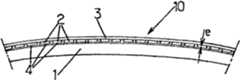
图1所示的光学元件10是用于软焦点透镜组(spectacle lens)的半成品。该半成品可以具有例如6cm的直径。在本身已知的方式中,准备用框架组装的该透镜是通过沿着与该框架对应的轮廓修整该半成品10而得到的。这个轮廓在图1中用虚线示出。The
图2a和2b示出光学元件的两个最初的配置,其对应于在透镜中限定光学功能刻入的像素的两种不同方式。在依照图2a配置的情况下,像素在照射阶段之前不被限定在光学元件中。相反,具有依照图2b配置的光学元件最初具有像素,这些像素在光学元件的制造期间由它们各自的尺寸、它们各自的形状和它们各自的结构单独限定。Figures 2a and 2b show two initial configurations of the optical elements, corresponding to two different ways of defining optically functionally inscribed pixels in the lens. In the case of the configuration according to Fig. 2a, the pixels are not confined in the optical element before the illumination phase. In contrast, an optical element having a configuration according to Fig. 2b initially has pixels which are individually defined by their respective size, their respective shape and their respective structure during the manufacture of the optical element.
依照光学元件的第一种配置(图2a),有源材料分布在元件至少一部分中的基本上连续的层内。透镜10半成品因此由透明无机物或者有机材料的基板1组成,以一层连续的有源材料2覆盖在基板的一面上。该层有源材料2可以在基板1的整个面上具有均匀的厚度。可选择地,有源材料层2本身可以用至少一个涂层3覆盖。这样的涂层3可以特别地具有一个抗反射涂层、一个赋予该透镜改善的抗刮擦性的硬涂层,或者一个防水涂层。可以将该层有源材料2和涂层3通过本领域技术人员已知的方法之一涂覆到基板1上。According to a first configuration of the optical element (Fig. 2a), the active material is distributed in a substantially continuous layer in at least a part of the element. The
根据第二种配置(图2b),该有源材料分布在彼此分开的部分4上并且形成在该元件的至少一部分中。作为实例,部分4布置在具有透明材料的基板1的一个表面上。它们彼此相邻并且形成一个网状物,以覆盖基板1的整个上表面。部分4能够直接形成在基板1上或者形成在添加到基板1的一层附加材料上。有源材料2的每一部分具有厚度e。也可以在部分4上放置涂层3。According to a second configuration ( FIG. 2 b ), the active material is distributed over
优选地,在光学元件的各种可能的配置中,有源材料2的厚度e在该元件中大于10μm。从调制该有源材料2的光学性能中得到的光学功能由此可以具有高的振幅。例如,在有源材料2吸收系数调制的情况下,能够得到非常暗的透镜。这是因为吸收性的有源材料的厚度足以获得相当少的光亮度,例如达到入射光90%的比例。这个有创造性的方法因此能够制造具有有效保护性的太阳镜。Preferably, in each possible configuration of the optical element, the thickness e of the active material 2 is greater than 10 μm in the element. The optical functions resulting from modulating the optical properties of the active material 2 can thus have high amplitudes. For example, in the case of active material 2 absorption coefficient modulation, very dark lenses can be obtained. This is because the thickness of the absorbing active material is sufficient to obtain relatively little luminance, for example up to 90% of the incident light. This inventive approach thus enables the manufacture of effective protective sunglasses.
类似地,当调制的光学性能是有源材料的折射性时,能够得到强有效的眼反常矫正。这是因为,由于从调制折射率得到的光路的改变与有源材料的厚度成比例,因此其超过10μm的厚度能够在透镜表面各个点之间获得光路的大范围变化。Similarly, when the modulated optical property is the refractive property of the active material, a strong and effective correction of ocular abnormalities can be obtained. This is because, since the change in the optical path resulting from modulating the refractive index is proportional to the thickness of the active material, its thickness exceeding 10 μm enables a wide range of variation in the optical path between various points on the lens surface.
能够以各种方式来实现照射有源材料2,以在透镜10半成品刻入光学功能。特别地,它能够由将有源材料2通过一个掩模在合适的光束中曝光而实现。这样的掩模具有相对该光束基本上透明的区域、部分透明的区域和/或不透明区域。通过选择由该有源材料2的每部分所接受的光束能量的量,该光学性能就以预定的等级固定在这部分中。由每部分接受的光束能量的量可以通过改变光束的功率和/或者曝光时间来改变。Irradiating the active material 2 to inscribe an optical function in the
用于照射有源材料的各部分的光束可以是不同的类型:电磁辐射束、特别是紫外线辐射、或者电子束。可以根据光束类型使用和选择已知的照射源。此外,在照射期间,可以对有源材料2的所有部分都同时曝光,或者能够对有源材料2的某些部分相继照射。The beams used to irradiate the parts of the active material can be of different types: beams of electromagnetic radiation, in particular ultraviolet radiation, or beams of electrons. Known sources of illumination can be used and selected according to beam type. Furthermore, during irradiation, all parts of the active material 2 can be exposed simultaneously, or certain parts of the active material 2 can be irradiated sequentially.
有利地,对照射进行控制,使得能够根据用于量化这个性能的预定值对光学性能不连续地调制。因而能够对照射使用数字控制,这很容易以编程来进行。对于可以非常精确地限定该透镜的光学功能来说,该预定值优选包括至少十个截然不同的值。Advantageously, the illumination is controlled such that the optical property can be modulated discontinuously according to a predetermined value quantifying this property. It is thus possible to use digital control of the irradiation, which is easily programmed. For the optical function of the lens to be defined very precisely, the predetermined value preferably comprises at least ten distinct values.
图3示出本发明的一个优选实施例,其不需要使用用于照射的掩模。该透镜半成品10能够是上述第一种或者第二种配置中的一种。照射是利用产生例如紫外光的光束101的激光器100来实施的。将半成品10放在光束101的前面。调整激光器100和半成品10之间的距离,使有源材料2定位在光束101的会聚点。使光束101平行于半成品10的表面移动,以在连续的曝光中照射有源材料2的不同部分。由此获得对光学功能的刻入,并具有平行于半成品表面的高分辨率。当半成品10包括涂层3时,这个涂层相对光束101必须是透明的。Figure 3 shows a preferred embodiment of the invention which does not require the use of a mask for illumination. The lens
在刻入光学功能期间的激光束驱动器和定位机构可以是那些在光盘蚀刻机器中通常采用的类型。通过使用一个用于描述要提供的光学功能数量的计算机文件,来控制这些机构和激光器能量供给,以实施在不同像素之间对有源材料的光学性能进行期望的调制。The laser beam drive and positioning mechanism during the inscription optical function may be of the type commonly employed in optical disc etching machines. These mechanisms and laser energy supply are controlled by using a computer file describing the amount of optical function to be provided to implement the desired modulation of the optical properties of the active material between the different pixels.
如图2a所示,当将有源材料2最初分布在半成品10的连续层中时,有源材料2的对应于不同像素的各部分的形状在照射期间确定。如果照射是通过掩模实现的,那么这些像素复制该掩模的图案。如果照射是使用聚焦光束实现的,那么这些像素对应于在连续的曝光期间位于该层有源材料内的光束的截面。As shown in Figure 2a, when the active material 2 is initially distributed in successive layers of the
图4a示出用于具有图2a所示配置的半成品10的像素的一种可能分布。这个分布通过基本上圆形的像素5对应于一个网格。P是两个相邻像素之间的距离,并且当根据图3实施照射时,对应于光束101的基本平移距离。D是每个像素5的直径,并且在有源材料2的级别上基本上对应于激光束101的直径。Fig. 4a shows one possible distribution of pixels for a
如图2b所示,当将有源材料2最初分布在半成品10的分离的各部分中时,对该照射条件进行调整,使得有源材料2的每个部分4在相同的条件下曝光于辐射中。对光学性能的调制因而基于在照射之前该分布和各部分存在的形状。根据图4b,部分4每个都可以为具有宽度D的六边形,并且两个相邻的部分由一个厚度为d的壁分开。网格间距P因而等于D和d的和。As shown in Figure 2b, when the active material 2 is initially distributed in separate parts of the
通常,间距P优选在5μm和100μm之间。透镜因而具有一致的、没有一点晕彩的视觉外观。例如D可以等于20μm,并且对按照有源材料的最初的分离各部分的实施情况来说,d可以等于0.2μm。半成品10的表面因而包括大量形成像素的有源材料2的部分,在其每个部分中的光学功能被调整。例如,能够使用超过一百万个像素。In general, the pitch P is preferably between 5 μm and 100 μm. The lenses thus have a consistent visual appearance free of any iridescence. For example D can be equal to 20 μm, and d can be equal to 0.2 μm for the implementation according to the initial separation of parts of the active material. The surface of the
光学元件表面的像素网格能够是任何形状。特别地,有源材料的受照部分可以以六边形网格分布在元件中。这样的网格允许对于有源材料的各部分的无数形状来说光学元件表面具有高的会聚率。特别地,当像素是圆形的(图4a)或者六边形(图4b)时,六边形网格是合适的。The pixel grid on the surface of the optical element can be of any shape. In particular, the illuminated portions of the active material may be distributed in the element in a hexagonal grid. Such a mesh allows high convergence ratios of the optical element surface for countless shapes of portions of active material. In particular, a hexagonal grid is suitable when the pixels are circular (Fig. 4a) or hexagonal (Fig. 4b).
在某些情况下,以不规则的网格来分布像素是有利的。不想要的衍射效应能够由此得到消除。在某些情况下并且根据发明的需要,像素也可以是方的或者矩形的。也可以将像素的各种形状结合起来。In some cases it is advantageous to distribute the pixels on an irregular grid. Unwanted diffraction effects can thereby be eliminated. In some cases and depending on the needs of the invention, the pixels may also be square or rectangular. It is also possible to combine various shapes of pixels.
有源材料2可以包括光引发剂和/或光聚合物。当在合适的条件下实施照射时光引发剂和/或光聚合物对照射是敏感的。Active material 2 may comprise photoinitiators and/or photopolymers. The photoinitiator and/or photopolymer are sensitive to irradiation when the irradiation is carried out under suitable conditions.
文献EP1225458和US6309803描述了对波长为365nm(纳米)的紫外光敏感的有源材料。这种有源材料能够在两种不同的相位聚合,该相位是通过施加到光学元件上的聚合条件来选择的。第一相位对应于有机聚合网络。其在有源材料受到照射时形成。第二相位对应于无机聚合网格,并且其在有源材料受到加热时形成。第一相位的折射率低于第二相位的折射率。Documents EP1225458 and US6309803 describe active materials sensitive to ultraviolet light with a wavelength of 365 nm (nanometers). This active material is capable of polymerizing in two different phases selected by the polymerizing conditions applied to the optical element. The first phase corresponds to the organic aggregate network. It is formed when the active material is irradiated. The second phase corresponds to the inorganic polymeric network and it forms when the active material is heated. The refractive index of the first phase is lower than the refractive index of the second phase.
这种有源材料2能够通过将基板1浸渍在前体(precursor)溶液中而被沉积在基板1上。这种沉积过程一般称为“浸渍涂布”。该溶液包括能够在一起形成有机聚合网格或者无机聚合网格的两种前体。这两种前体是3-(三甲氧基硅烷)丙甲基丙烯酸酯以及n-丙氧化锆和甲基丙烯酸反应的产品。将可从例如供应商CIBA购得的Irgacure 1800进一步添加到前体溶液中。在将基板1浸渍在前体溶液中之后,将基板1加热到一个等于60℃或者更高的温度大约30分钟。由此在基板1上得到一个有源材料2的干燥层。This active material 2 can be deposited on the substrate 1 by dipping the substrate 1 in a precursor solution. This deposition process is generally referred to as "dip coating". The solution includes two precursors capable of forming together an organic polymeric network or an inorganic polymeric network. These two precursors are 3-(trimethoxysilane)propyl methacrylate and the product of the reaction of n-zirconium propoxide and methacrylic acid. Irgacure 1800, commercially available eg from the supplier CIBA, was further added to the precursor solution. After the substrate 1 is immersed in the precursor solution, the substrate 1 is heated to a temperature equal to 60° C. or higher for about 30 minutes. A dry layer of active material 2 is thus obtained on the substrate 1 .
当将如此获得的有源材料2的一部分用波长为365nm的紫外光照射时,就形成了有机聚合网格,其密度依赖于照射时间和强度。然后将基板1加热到等于100℃或者更高的温度20到45分钟。因此形成无机聚合网格。在有源材料2没有被预先照射的那些部分产生具有高折射率的纯相位。在有源材料被预先照射的那些部分,无机聚合网格从没有被有机聚合反应消耗的前体的数量中形成。由此在受照部分获得一个中间折射率值,其位于对应于纯无机网格和纯有机网格的两个极限值之间。When a part of the active material 2 thus obtained was irradiated with ultraviolet light having a wavelength of 365 nm, an organic polymeric network was formed, the density of which depended on the irradiation time and intensity. The substrate 1 is then heated to a temperature equal to 100° C. or higher for 20 to 45 minutes. An inorganic polymeric network is thus formed. A pure phase with a high refractive index results in those parts of the active material 2 which have not been pre-irradiated. In those parts where the active material is pre-irradiated, the inorganic polymeric network is formed from the amount of precursor not consumed by the organic polymerisation reaction. An intermediate refractive index value is thus obtained in the irradiated portion, which lies between the two limit values corresponding to purely inorganic and purely organic meshes.
一旦完成根据无机网格加热的聚合,两种前体就完全消耗掉。因而有源材料2对位于波长365nm处的紫外光的另外的照射不敏感。Both precursors are completely consumed once the polymerization according to the heating of the inorganic grid is completed. The active material 2 is thus insensitive to further irradiation of ultraviolet light at a wavelength of 365 nm.
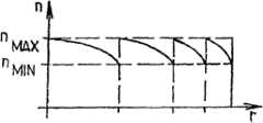
在本发明的特定实施例中,对照射进行控制,使得对光学性能的调制在有源材料的某些相邻部分表现出跳跃(jumps)。图5a示出具有可改性折射性的有源材料的这种变化的一个例子。折射率的分布仅仅依赖于这层有源材料2的一点和半成品10的中心之间的距离r。距离r绘在x轴上,而折射率n的值绘在y轴上。半成品10分为同心环Z1-Z4。在每个环Z1-Z4内,折射率n在用nMIN表示的最小值和用nMAX表示的最大值之间逐渐变化(连续地或者对应于刻入系统的分辨率的基本跳跃)。在两个连续环的边界处,折射率从值nMAX跳跃到值nMIN。由此得到的光学元件具有发散菲涅耳透镜的功能,同时具有一致的厚度。由此得到近视矫正透镜,其具有的光学强度高于根据本发明所述制备的、具有在半成品的整个表面上折射率连续变化的透镜的光学强度。In a particular embodiment of the invention, the illumination is controlled such that the modulation of the optical properties exhibits jumps in certain adjacent portions of the active material. Figure 5a shows an example of such a variation of an active material with modifiable refraction. The distribution of the refractive index depends only on the distance r between a point of this layer of active material 2 and the center of the
图5b对应于图5a,是用于远视矫正透镜。得到的光学功能是会聚菲涅耳透镜的功能。Fig. 5b corresponds to Fig. 5a and is a corrective lens for hyperopia. The resulting optical function is that of a converging Fresnel lens.
在本发明的某些特定的实施例中,光学元件结合了多种经选择的有源材料,使得每种有源材料各自的光学性能可通过照射光学元件而选择性地改变。每种有源材料平行于元件的表面分布。通过在对应于每种有源材料的合适的条件下照射该元件,因而能够针对每种有源材料将截然不同的光学功能刻入到光学元件中。光学元件的全部光学功能因而对应于使用每种有源材料刻入的光学功能的叠加而产生。当刻入的光学功能是可累加(cumulable)类型时,全部的光学功能可以具有特别高的振幅。例如,如果每种有源材料的刻入对应近视矫正功能,那么可以得到适于特别高的近视度数的透镜。In certain specific embodiments of the invention, the optical element incorporates multiple selected active materials such that the respective optical properties of each active material can be selectively altered by illuminating the optical element. Each active material is distributed parallel to the surface of the component. By illuminating the element under suitable conditions corresponding to each active material, distinct optical functions can thus be engraved into the optical element for each active material. The entire optical function of the optical element thus results corresponding to the superposition of the optical functions inscribed with each active material. When the inscribed optical functions are of the cumulative type, all optical functions can have a particularly high amplitude. For example, if the inscription of each active material corresponds to a myopia correcting function, lenses suitable for particularly high degrees of myopia can be obtained.
有利地,使有源材料分布在位于光学元件内叠加的各个层内。因而能够简单地制得光学元件。特别地,对各层中的每一层使用合适的沉积方法,可以将有源材料连续地沉积或者添加到基板上。图6示出一个透镜10半成品,其包括基板1,具有叠加在其一个表面上的、以2a-2c标记的三个不同层的有源材料。Advantageously, the active material is distributed in layers superimposed within the optical element. Therefore, an optical element can be produced simply. In particular, the active material can be successively deposited or added to the substrate using a suitable deposition method for each of the layers. Figure 6 shows a
用于选择性改变该有源材料之一的光学性能的照射条件能够通过在每个有源材料中结合的至少一种光引发剂来决定。由此,各种有源材料有利地包含对不同波长的照射敏感的各自的光引发剂。The irradiation conditions for selectively changing the optical properties of one of the active materials can be determined by at least one photoinitiator incorporated in each active material. Thus, the various active materials advantageously contain respective photoinitiators that are sensitive to radiation of different wavelengths.
应该理解,在本发明的上下文中,基板1可以具有其自己的光学功能。基板1的这个光学功能因而与通过有源材料2对光学性能的调制所提供的光学功能叠加或者累加起来。例如,基板1可以是吸收性材料,其为最终的透镜赋予防太阳光的功能,并且有源材料的照射可以赋予眼反常矫正功能。由此得到既防太阳光又具有矫正性的透镜。基板1自身也可以具有矫正功能,这可以特别地从位于基板1的中心和外围之间的厚度差异而得到。因而,通过对有源材料2折射性的调制而提供的额外的眼反常矫正的光学功能就与基板1的矫正功能累加在一起。It should be understood that, in the context of the present invention, the substrate 1 may have its own optical function. This optical function of the substrate 1 is thus superimposed or summed up with the optical function provided by the modulation of the optical properties by the active material 2 . For example, the substrate 1 may be an absorbing material which confers a sun protection function to the final lens, and the illumination of the active material may confer an eye paralysis correction function. The result is a lens that is both sun-blocking and corrective. The substrate 1 itself may also have a rectifying function, which may in particular result from the difference in thickness between the center and the periphery of the substrate 1 . Thus, the additional optical function of ocular abnormality correction provided by the modulation of the refractive properties of the active material 2 is added to the corrective function of the substrate 1 .
最后,尽管本发明已经针对眼镜片做出详细的描述,但是也可以理解,可以将其同样地应用到其它眼科元件例如头盔护目镜、或者面具透镜中。这可以例如是乘机车者或者飞行员的头盔,或者跳水或者登山者的面具。Finally, although the invention has been described in detail with respect to spectacle lenses, it is to be understood that it can be equally applied to other ophthalmic components such as helmet visors, or mask lenses. This can be, for example, a motorcyclist's or pilot's helmet, or a diver's or mountaineer's mask.
Claims (28)
Applications Claiming Priority (3)
| Application Number | Priority Date | Filing Date | Title |
|---|---|---|---|
| FR0407388AFR2872590B1 (en) | 2004-07-02 | 2004-07-02 | METHOD FOR PRODUCING AN OPHTHALMIC GLASS AND OPTICAL COMPONENT SUITABLE FOR CARRYING OUT SAID METHOD |
| FR0407388 | 2004-07-02 | ||
| PCT/FR2005/001635WO2006013252A1 (en) | 2004-07-02 | 2005-06-28 | Method for producing an ophthalmic lens and an optical component for carrying out said method |
Publications (2)
| Publication Number | Publication Date |
|---|---|
| CN1981232A CN1981232A (en) | 2007-06-13 |
| CN1981232Btrue CN1981232B (en) | 2010-04-07 |
Family
ID=34946960
Family Applications (1)
| Application Number | Title | Priority Date | Filing Date |
|---|---|---|---|
| CN2005800226149AExpired - LifetimeCN1981232B (en) | 2004-07-02 | 2005-06-28 | Method for manufacturing ophthalmic lens and optical element suitable for carrying out said method |
Country Status (10)
| Country | Link |
|---|---|
| US (1) | US8092017B2 (en) |
| EP (1) | EP1763698B1 (en) |
| JP (1) | JP4974889B2 (en) |
| KR (1) | KR101256997B1 (en) |
| CN (1) | CN1981232B (en) |
| AU (1) | AU2005268737B2 (en) |
| BR (1) | BRPI0512879A (en) |
| CA (1) | CA2571374A1 (en) |
| FR (1) | FR2872590B1 (en) |
| WO (1) | WO2006013252A1 (en) |
Families Citing this family (12)
| Publication number | Priority date | Publication date | Assignee | Title |
|---|---|---|---|---|
| FR2908897B1 (en)* | 2006-11-17 | 2009-03-06 | Essilor Int | COLORFUL COLOR OPHTHALMIC LENSES. |
| US20090164008A1 (en)* | 2007-12-21 | 2009-06-25 | Xin Hong | Lens surface with combined diffractive, toric, and aspheric components |
| US9720253B2 (en) | 2008-12-22 | 2017-08-01 | The Medical College Of Wisconsin | Method and apparatus for limiting growth of eye length |
| FR2972814B1 (en) | 2011-03-16 | 2014-04-18 | Essilor Int | TRANSPARENT OPTICAL ELEMENT WITH SEVERAL LAYERS CONSISTING OF CELLULAR PAVAGES |
| US10268050B2 (en) | 2015-11-06 | 2019-04-23 | Hoya Lens Thailand Ltd. | Spectacle lens |
| MY203940A (en) | 2016-08-01 | 2024-07-25 | Univ Washington | Ophthalmic lenses for treating myopia |
| US11718052B2 (en) | 2017-05-08 | 2023-08-08 | Sightglass Vision, Inc. | Contact lenses for reducing myopia and methods for making the same |
| US10884264B2 (en) | 2018-01-30 | 2021-01-05 | Sightglass Vision, Inc. | Ophthalmic lenses with light scattering for treating myopia |
| KR20210066789A (en) | 2018-07-12 | 2021-06-07 | 사이트글래스 비전 인코포레이티드 | Methods and devices for reducing myopia in children |
| EP3931626A4 (en) | 2019-03-01 | 2023-03-15 | Sightglass Vision, Inc. | Ophthalmic lenses for reducing myopic progression and methods of making the same |
| SG11202110890YA (en) | 2019-04-23 | 2021-10-28 | Sightglass Vision Inc | Ophthalmic lenses with dynamic optical properties for reducing development of myopia |
| DE102023116999A1 (en)* | 2023-06-28 | 2025-01-02 | Carl Zeiss Ag | Spectacle lens, spectacles, computer-implemented method for designing a spectacle lens and method for producing a spectacle lens |
Family Cites Families (106)
| Publication number | Priority date | Publication date | Assignee | Title |
|---|---|---|---|---|
| US2196066A (en) | 1938-03-02 | 1940-04-02 | Feinbloom William | Contact lens |
| US2511329A (en) | 1946-12-26 | 1950-06-13 | Craig Edward | Lens shield |
| US3460960A (en) | 1965-05-03 | 1969-08-12 | Owens Illinois Inc | Coated glass and method of making same |
| US3532038A (en) | 1967-06-05 | 1970-10-06 | Ibm | Multi-lens devices for the fabrication of semiconductor devices |
| US3628854A (en) | 1969-12-08 | 1971-12-21 | Optical Sciences Group Inc | Flexible fresnel refracting membrane adhered to ophthalmic lens |
| US3978580A (en) | 1973-06-28 | 1976-09-07 | Hughes Aircraft Company | Method of fabricating a liquid crystal display |
| US4150878A (en) | 1974-04-05 | 1979-04-24 | Giorgio Barzilai | Hollow-space cell and method for its manufacture |
| US4268132A (en) | 1979-09-24 | 1981-05-19 | Neefe Charles W | Oxygen generating contact lens |
| CH666560A5 (en) | 1983-03-01 | 1988-07-29 | Tadeusz Bobak | DISPLAY DEVICE. |
| JPS60188925A (en) | 1984-03-09 | 1985-09-26 | Canon Inc | Manufacturing method of optical modulation element |
| US4601545A (en) | 1984-05-16 | 1986-07-22 | Kern Seymour P | Variable power lens system |
| US4621912A (en) | 1985-02-14 | 1986-11-11 | Meyer Donald R | Foraminated optical contact lens |
| IT1190508B (en) | 1986-03-24 | 1988-02-16 | Daniele Senatore | ADJUSTABLE TRANSPARENCY GLASSES |
| US5017000A (en) | 1986-05-14 | 1991-05-21 | Cohen Allen L | Multifocals using phase shifting |
| IL85860A (en) | 1988-03-24 | 1992-06-21 | Amir Cohen | Contact lens |
| US4994664A (en) | 1989-03-27 | 1991-02-19 | Massachusetts Institute Of Technology | Optically coupled focal plane arrays using lenslets and multiplexers |
| FR2647789B1 (en) | 1989-06-05 | 1994-07-22 | Essilor Int | INDOLINO-SPIRO-OXAZINE PHOTOCHROMIC COMPOUNDS, PROCESS FOR THEIR PREPARATION, PHOTOCHROMIC COMPOSITIONS AND ARTICLES CONTAINING SUCH COMPOUNDS |
| FR2670210A1 (en) | 1990-12-06 | 1992-06-12 | Essilor Int | NOVEL PHOTOCHROMIC COMPOUNDS OF THE INDOLINO-SPIRO-BENZOXAZINE TYPE AND THEIR PREPARATION PROCESS. |
| US5359444A (en)* | 1992-12-24 | 1994-10-25 | Motorola, Inc. | Auto-focusing optical apparatus |
| US5576870A (en) | 1993-04-23 | 1996-11-19 | Matsushita Electric Industrial Co., Ltd. | Liquid crystal display panel having a phase grating formed of liquid crystal molecules |
| FR2712593B1 (en) | 1993-11-17 | 1996-01-05 | Essilor Int | New spirooxazines and their use in the field of ophthalmic optics. |
| US5585968A (en)* | 1993-12-01 | 1996-12-17 | International Business Machines Corporation | Optical elements having regions of different indices of refraction and method of fabricating the same |
| FR2718446B1 (en) | 1994-04-06 | 1997-01-03 | Essilor Int | Heteroannelated Spiro [fluorene- [2H] -benzopyranes] and their use in the field of ophthalmic optics. |
| FR2718447B1 (en) | 1994-04-06 | 1996-05-24 | Essilor Int | Chromenes of the 2,2-diphenyl type heteroannelated in 6.7 and their use in the field of ophthalmic optics. |
| US5699142A (en) | 1994-09-01 | 1997-12-16 | Alcon Laboratories, Inc. | Diffractive multifocal ophthalmic lens |
| FR2731081B1 (en) | 1995-02-27 | 1997-04-11 | Essilor Int | PROCESS FOR OBTAINING A TRANSPARENT ARTICLE WITH A REFRACTION INDEX |
| US6707516B1 (en) | 1995-05-23 | 2004-03-16 | Colorlink, Inc. | Single-panel field-sequential color display systems |
| US6274288B1 (en)* | 1995-06-12 | 2001-08-14 | California Institute Of Technology | Self-trapping and self-focusing of optical beams in photopolymers |
| FR2740231B1 (en) | 1995-10-20 | 1998-03-06 | Christian Dalloz Sa | DRAFT FOR NON-CORRECTOR EYEPIECE |
| US5905561A (en) | 1996-06-14 | 1999-05-18 | Pbh, Inc. | Annular mask lens having diffraction reducing edges |
| US5733077A (en) | 1996-07-02 | 1998-03-31 | The Hilsinger Company Lp | Lens drill guide |
| GB2315900B (en) | 1996-07-26 | 2000-10-04 | Sharp Kk | Liquid crystal device |
| US5774273A (en) | 1996-08-23 | 1998-06-30 | Vari-Lite, Inc. | Variable-geometry liquid-filled lens apparatus and method for controlling the energy distribution of a light beam |
| US5812235A (en) | 1996-09-04 | 1998-09-22 | Pemrable Technologies Inc. | Multifocal corneal contact lenses |
| US5763054A (en) | 1996-09-13 | 1998-06-09 | Trw Inc. | Anti-reflection treatment for optical elements |
| US5764333A (en) | 1997-02-27 | 1998-06-09 | Somsel; John R. | Sunshields for eyeglasses |
| DE19714434A1 (en) | 1997-04-08 | 1998-10-15 | Armin Schaeuble | Selective electronic photo-protective spectacles |
| FR2763070B1 (en) | 1997-05-06 | 1999-07-02 | Essilor Int | NOVEL SPIROOXAZINE PHOTOCHROMIC COMPOUNDS, THEIR USE IN THE FIELD OF OPHTHALMIC OPTICS |
| US5914802A (en) | 1997-07-18 | 1999-06-22 | Northrop Grumman Corporation | Combined spatial light modulator and phase mask for holographic storage system |
| US6262789B1 (en) | 1998-11-27 | 2001-07-17 | Zvi Yaniv | Liquid display and method of making same |
| EP1173790A2 (en) | 1999-03-01 | 2002-01-23 | Boston Innovative Optics, Inc. | System and method for increasing the depth of focus of the human eye |
| WO2000054101A1 (en) | 1999-03-05 | 2000-09-14 | Seiko Epson Corporation | Electrophoresis display and its production method |
| US6327072B1 (en) | 1999-04-06 | 2001-12-04 | E Ink Corporation | Microcell electrophoretic displays |
| US6871951B2 (en) | 2000-06-23 | 2005-03-29 | E-Vision, Llc | Electro-optic lens with integrated components |
| DE19927361A1 (en) | 1999-06-16 | 2000-12-21 | Creavis Tech & Innovation Gmbh | Electrophoretic displays |
| FR2795361B1 (en) | 1999-06-22 | 2001-09-07 | Essilor Int | OPHTHALMIC LENS MOLDING PROCESS |
| US6309803B1 (en) | 1999-07-01 | 2001-10-30 | Lumenon, Innovative Lightwave Technology, Inc. | On-substrate cleaving of sol-gel waveguide |
| AU779628B2 (en) | 1999-07-08 | 2005-02-03 | Essilor International Compagnie Generale D'optique | Bi-or terthienyl substituted photochromic naphtho(2,1-b)pyran compounds |
| US6781666B2 (en) | 1999-07-16 | 2004-08-24 | Minolta Co., Ltd. | Liquid crystal display and method to manufacture the same |
| US6307243B1 (en) | 1999-07-19 | 2001-10-23 | Micron Technology, Inc. | Microlens array with improved fill factor |
| US6395124B1 (en)* | 1999-07-30 | 2002-05-28 | 3M Innovative Properties Company | Method of producing a laminated structure |
| US6199986B1 (en)* | 1999-10-21 | 2001-03-13 | University Of Rochester | Rapid, automatic measurement of the eye's wave aberration |
| US6672921B1 (en) | 2000-03-03 | 2004-01-06 | Sipix Imaging, Inc. | Manufacturing process for electrophoretic display |
| US6577434B2 (en) | 2000-01-14 | 2003-06-10 | Minolta Co., Ltd. | Variable focal position spatial modulation device |
| US6281366B1 (en) | 2000-02-29 | 2001-08-28 | Essilor International Compagnie Generale D'optique | Photochromic [3H]naphtho[2,1-b]pyran compounds containing an acetylenic substituent, process for their manufacture, and photochromic materials and articles obtained |
| US6829078B2 (en) | 2000-03-03 | 2004-12-07 | Sipix Imaging Inc. | Electrophoretic display and novel process for its manufacture |
| WO2001071411A2 (en)* | 2000-03-20 | 2001-09-27 | California Institute Of Technology | Application of wavefront sensor to lenses capable of post-fabrication power modification |
| JP4116224B2 (en) | 2000-03-23 | 2008-07-09 | ローム株式会社 | Manufacturing method of lens array |
| US6301051B1 (en) | 2000-04-05 | 2001-10-09 | Rockwell Technologies, Llc | High fill-factor microlens array and fabrication method |
| JP4006925B2 (en) | 2000-05-30 | 2007-11-14 | セイコーエプソン株式会社 | Method for manufacturing electrophoretic display device |
| US6485599B1 (en) | 2000-07-11 | 2002-11-26 | International Business Machines Corporation | Curing of sealants using multiple frequencies of radiation |
| JP2002221616A (en)* | 2000-11-21 | 2002-08-09 | Seiko Epson Corp | Color filter manufacturing method and manufacturing apparatus, liquid crystal device manufacturing method and manufacturing apparatus, EL device manufacturing method and manufacturing apparatus, inkjet head control apparatus, material discharging method and material discharging apparatus, and electronic equipment |
| US6813082B2 (en)* | 2000-11-27 | 2004-11-02 | Ophthonix, Inc. | Wavefront aberrator and method of manufacturing |
| US7293871B2 (en)* | 2000-11-27 | 2007-11-13 | Ophthonix, Inc. | Apparatus and method of correcting higher-order aberrations of the human eye |
| ATE334412T1 (en)* | 2001-01-19 | 2006-08-15 | Centre Nat Rech Scient | METHOD FOR PRODUCING A WAVEGUIDE COMPONENT WITH MULTIPLE LAYERS ON A SUBSTRATE AND COMPONENT PROVIDED THEREFROM |
| WO2002077672A2 (en) | 2001-02-07 | 2002-10-03 | Corning Incorporated | High-contrast screen with random microlens array |
| TW556044B (en) | 2001-02-15 | 2003-10-01 | Sipix Imaging Inc | Process for roll-to-roll manufacture of a display by synchronized photolithographic exposure on a substrate web |
| WO2002067020A2 (en) | 2001-02-19 | 2002-08-29 | Koninklijke Philips Electronics N.V. | Optical element and method of manufacturing such an optical element |
| US6753067B2 (en) | 2001-04-23 | 2004-06-22 | Sipix Imaging, Inc. | Microcup compositions having improved flexure resistance and release properties |
| US7184066B2 (en) | 2001-05-09 | 2007-02-27 | Clairvoyante, Inc | Methods and systems for sub-pixel rendering with adaptive filtering |
| KR100701442B1 (en) | 2001-05-10 | 2007-03-30 | 엘지.필립스 엘시디 주식회사 | Inkjet liquid crystal coating method |
| US7205355B2 (en) | 2001-06-04 | 2007-04-17 | Sipix Imaging, Inc. | Composition and process for the manufacture of an improved electrophoretic display |
| US7217375B2 (en)* | 2001-06-04 | 2007-05-15 | Ophthonix, Inc. | Apparatus and method of fabricating a compensating element for wavefront correction using spatially localized curing of resin mixtures |
| US6788452B2 (en) | 2001-06-11 | 2004-09-07 | Sipix Imaging, Inc. | Process for manufacture of improved color displays |
| US6982178B2 (en) | 2002-06-10 | 2006-01-03 | E Ink Corporation | Components and methods for use in electro-optic displays |
| TW527529B (en) | 2001-07-27 | 2003-04-11 | Sipix Imaging Inc | An improved electrophoretic display with color filters |
| CN1539092A (en) | 2001-08-07 | 2004-10-20 | 金炯植 | Lens fixing apparatus for rimless spectacle |
| TW539928B (en) | 2001-08-20 | 2003-07-01 | Sipix Imaging Inc | An improved transflective electrophoretic display |
| US6712466B2 (en)* | 2001-10-25 | 2004-03-30 | Ophthonix, Inc. | Eyeglass manufacturing method using variable index layer |
| TW574566B (en) | 2001-10-31 | 2004-02-01 | Optrex Kk | Liquid crystal display element |
| CN1221842C (en) | 2002-01-23 | 2005-10-05 | 索尼公司 | Image display and image projector |
| US6860601B2 (en) | 2002-02-06 | 2005-03-01 | John H. Shadduck | Adaptive optic lens system and method of use |
| US6963435B2 (en) | 2002-03-27 | 2005-11-08 | Avery Dennison Corporation | Switchable electro-optical laminates |
| US6836371B2 (en) | 2002-07-11 | 2004-12-28 | Ophthonix, Inc. | Optical elements and methods for making thereof |
| US6966649B2 (en) | 2002-08-12 | 2005-11-22 | John H Shadduck | Adaptive optic lens system and method of use |
| US7036932B2 (en) | 2002-10-04 | 2006-05-02 | Vision-Ease Lens | Laminated functional wafer for plastic optical elements |
| AU2003294418B2 (en) | 2002-11-20 | 2009-07-16 | Powervision, Inc. | Lens system and method for power adjustment |
| US20040120667A1 (en) | 2002-12-23 | 2004-06-24 | Eastman Kodak Company | Walled network optical component |
| US6914658B2 (en) | 2002-12-26 | 2005-07-05 | Intel Corporation | Method for fabricating a moat around an active pixel area of a microelectronic image projection device |
| US7245439B2 (en) | 2003-07-14 | 2007-07-17 | Koninklijke Philips Electronics N.V. | Variable lens |
| EP1673656B1 (en)* | 2003-10-03 | 2007-01-17 | Invisia Ltd. | Multifocal lens |
| US7227692B2 (en) | 2003-10-09 | 2007-06-05 | Micron Technology, Inc | Method and apparatus for balancing color response of imagers |
| JPWO2005072039A1 (en) | 2004-01-21 | 2007-12-27 | 大日本印刷株式会社 | Front plate for display and manufacturing method thereof |
| US7036929B1 (en) | 2004-04-12 | 2006-05-02 | William Rolf Harvey | Method and device for the application and removal of disposable corrective optical film to an eyeglass lens |
| JP4996462B2 (en) | 2004-07-02 | 2012-08-08 | エシロール アンテルナシオナル (コンパニー ジェネラル ドプティック) | Transparent optical element manufacturing method, optical component related to the manufacturing method, and obtained optical element |
| FR2872589B1 (en) | 2004-07-02 | 2006-10-27 | Essilor Int | METHOD FOR PRODUCING A TRANSPARENT OPTICAL ELEMENT, OPTICAL COMPONENT INVOLVED IN THIS METHOD AND OPTICAL ELEMENT THUS OBTAINED |
| US7371804B2 (en)* | 2004-09-07 | 2008-05-13 | Ophthonix, Inc. | Monomers and polymers for optical elements |
| JP5064229B2 (en) | 2004-11-02 | 2012-10-31 | イー・ビジョン・エルエルシー | Compound lens |
| FR2879757B1 (en) | 2004-12-17 | 2007-07-13 | Essilor Int | METHOD FOR PRODUCING A TRANSPARENT OPTICAL ELEMENT, OPTICAL COMPONENT INVOLVED IN THIS METHOD AND OPTICAL ELEMENT THUS OBTAINED |
| US7533453B2 (en) | 2005-01-24 | 2009-05-19 | Yancy Virgil T | E-facet optical lens |
| FR2883984B1 (en) | 2005-04-04 | 2007-06-22 | Essilor Int | APPARATUS FOR CONFORMING PLANAR FILM TO AN OPTICAL LENS, METHODS OF FUNCTIONALIZING AN OPTICAL LENS USING THE SAME, AND LENS OBTAINED THEREBY |
| FR2888951B1 (en) | 2005-07-20 | 2008-02-08 | Essilor Int | RANDOMIZED PIXELLIZED OPTICAL COMPONENT, METHOD FOR MANUFACTURING THE SAME, AND USE THEREOF IN THE MANUFACTURE OF A TRANSPARENT OPTICAL ELEMENT |
| FR2888947B1 (en) | 2005-07-20 | 2007-10-12 | Essilor Int | OPTICAL CELL COMPONENT |
| FR2888950B1 (en) | 2005-07-20 | 2007-10-12 | Essilor Int | TRANSPARENT PIXELLIZED OPTICAL COMPONENT WITH ABSORBENT WALLS ITS MANUFACTURING METHOD AND USE IN FARICATION OF A TRANSPARENT OPTICAL ELEMENT |
| US7715107B2 (en) | 2006-04-25 | 2010-05-11 | Asml Netherlands B.V. | Optical element for correction of aberration, and a lithographic apparatus comprising same |
| FR2902105B1 (en) | 2006-06-13 | 2008-09-12 | Essilor Int | METHOD FOR BONDING A FILM TO A CURVED SUBSTRATE |
- 2004
- 2004-07-02FRFR0407388Apatent/FR2872590B1/ennot_activeExpired - Lifetime
- 2005
- 2005-06-28CNCN2005800226149Apatent/CN1981232B/ennot_activeExpired - Lifetime
- 2005-06-28JPJP2007518643Apatent/JP4974889B2/ennot_activeExpired - Fee Related
- 2005-06-28USUS11/571,324patent/US8092017B2/enactiveActive
- 2005-06-28EPEP05783801Apatent/EP1763698B1/ennot_activeExpired - Lifetime
- 2005-06-28BRBRPI0512879-0Apatent/BRPI0512879A/ennot_activeIP Right Cessation
- 2005-06-28KRKR1020067027632Apatent/KR101256997B1/ennot_activeExpired - Fee Related
- 2005-06-28WOPCT/FR2005/001635patent/WO2006013252A1/enactiveApplication Filing
- 2005-06-28AUAU2005268737Apatent/AU2005268737B2/ennot_activeCeased
- 2005-06-28CACA002571374Apatent/CA2571374A1/ennot_activeAbandoned
Also Published As
| Publication number | Publication date |
|---|---|
| CN1981232A (en) | 2007-06-13 |
| US8092017B2 (en) | 2012-01-10 |
| US20070247588A1 (en) | 2007-10-25 |
| AU2005268737B2 (en) | 2010-12-23 |
| CA2571374A1 (en) | 2006-02-09 |
| BRPI0512879A (en) | 2008-04-15 |
| KR20070050879A (en) | 2007-05-16 |
| KR101256997B1 (en) | 2013-04-26 |
| EP1763698B1 (en) | 2012-12-26 |
| EP1763698A1 (en) | 2007-03-21 |
| FR2872590B1 (en) | 2006-10-27 |
| FR2872590A1 (en) | 2006-01-06 |
| AU2005268737A1 (en) | 2006-02-09 |
| JP2008504584A (en) | 2008-02-14 |
| JP4974889B2 (en) | 2012-07-11 |
| WO2006013252A1 (en) | 2006-02-09 |
Similar Documents
| Publication | Publication Date | Title |
|---|---|---|
| CA2615487C (en) | Randomly pixellated optical component, its fabrication method and its use in the fabrication of a transparent optical element | |
| AU2005268735B2 (en) | Method for producing a transparent optical element, an optical component involved into said method and the thus obtained optical element | |
| CN1981232B (en) | Method for manufacturing ophthalmic lens and optical element suitable for carrying out said method | |
| US10146066B2 (en) | Process for manufacturing an ophthalmic lens using voxels and the lens thus obtained | |
| AU2006271585B2 (en) | Pixellized transparent optical component, comprising an absorbent coating, method for making same and use in an optical element | |
| US20090316110A1 (en) | Method for making a transparent optical element, optical component used in said method and resulting optical element | |
| US20080212023A1 (en) | Pixellized Optical Component with Apodized Walls, Method for Making Same and Use thereof in Making a Transparent Optical Element | |
| CN106164753A (en) | The eyeglass being increased material technology by multilamellar is produced | |
| KR20080042832A (en) | Optical components with cells | |
| JP7438463B2 (en) | How to manufacture eyeglass lenses | |
| JP2023542243A (en) | Manufacturing method for eyeglass lenses | |
| KR102698109B1 (en) | Pupil-scalable photochromic artificial iris of contract lens and manufacturing method thereof | |
| EP4417404A1 (en) | Method of manufacturing a coated spectacle lens comprising structures | |
| BRPI0512879B1 (en) | PROCESS FOR CARRYING OUT AN OPTALMIC LENS AND OPTICAL COMPONENT ADAPTED FOR THE APPLICATION OF THAT PROCESS |
Legal Events
| Date | Code | Title | Description |
|---|---|---|---|
| C06 | Publication | ||
| PB01 | Publication | ||
| C10 | Entry into substantive examination | ||
| SE01 | Entry into force of request for substantive examination | ||
| C14 | Grant of patent or utility model | ||
| GR01 | Patent grant | ||
| TR01 | Transfer of patent right | Effective date of registration:20180403 Address after:France Sharon Ton Le Pon Patentee after:ESSILOR INTERNATIONAL Address before:French sirloin pass Patentee before:ESSILOR INTERNATIONAL (COMPAGNIE GENERALE D'OPTIQUE) | |
| TR01 | Transfer of patent right | ||
| CX01 | Expiry of patent term | Granted publication date:20100407 | |
| CX01 | Expiry of patent term |