CN1976229A - Semiconductor integrated circuit and method of reducing leakage current - Google Patents
Semiconductor integrated circuit and method of reducing leakage currentDownload PDFInfo
- Publication number
- CN1976229A CN1976229ACNA2006101484587ACN200610148458ACN1976229ACN 1976229 ACN1976229 ACN 1976229ACN A2006101484587 ACNA2006101484587 ACN A2006101484587ACN 200610148458 ACN200610148458 ACN 200610148458ACN 1976229 ACN1976229 ACN 1976229A
- Authority
- CN
- China
- Prior art keywords
- circuit
- transistor
- source
- nmos
- pmos
- Prior art date
- Legal status (The legal status is an assumption and is not a legal conclusion. Google has not performed a legal analysis and makes no representation as to the accuracy of the status listed.)
- Pending
Links
- 239000004065semiconductorSubstances0.000titleclaimsabstractdescription115
- 238000000034methodMethods0.000titleclaimsabstractdescription24
- 239000000758substrateSubstances0.000claimsabstractdescription299
- 230000000694effectsEffects0.000claimsdescription120
- 230000005669field effectEffects0.000claimsdescription64
- 238000010586diagramMethods0.000description34
- 101150110971CIN7 geneProteins0.000description26
- 101150110298INV1 geneProteins0.000description26
- 101100397044Xenopus laevis invs-a geneProteins0.000description26
- 230000006870functionEffects0.000description10
- 230000007423decreaseEffects0.000description7
- 230000014759maintenance of locationEffects0.000description6
- 238000005513bias potentialMethods0.000description4
- 101100498759Saccharomyces cerevisiae (strain ATCC 204508 / S288c) DDI1 geneProteins0.000description2
- 238000007796conventional methodMethods0.000description1
Images


Classifications
- H—ELECTRICITY
- H03—ELECTRONIC CIRCUITRY
- H03K—PULSE TECHNIQUE
- H03K19/00—Logic circuits, i.e. having at least two inputs acting on one output; Inverting circuits
- H03K19/02—Logic circuits, i.e. having at least two inputs acting on one output; Inverting circuits using specified components
- H03K19/08—Logic circuits, i.e. having at least two inputs acting on one output; Inverting circuits using specified components using semiconductor devices
- H03K19/094—Logic circuits, i.e. having at least two inputs acting on one output; Inverting circuits using specified components using semiconductor devices using field-effect transistors
- H03K19/0944—Logic circuits, i.e. having at least two inputs acting on one output; Inverting circuits using specified components using semiconductor devices using field-effect transistors using MOSFET or insulated gate field-effect transistors, i.e. IGFET
- G—PHYSICS
- G11—INFORMATION STORAGE
- G11C—STATIC STORES
- G11C11/00—Digital stores characterised by the use of particular electric or magnetic storage elements; Storage elements therefor
- G11C11/21—Digital stores characterised by the use of particular electric or magnetic storage elements; Storage elements therefor using electric elements
- G11C11/34—Digital stores characterised by the use of particular electric or magnetic storage elements; Storage elements therefor using electric elements using semiconductor devices
- G11C11/40—Digital stores characterised by the use of particular electric or magnetic storage elements; Storage elements therefor using electric elements using semiconductor devices using transistors
- G11C11/41—Digital stores characterised by the use of particular electric or magnetic storage elements; Storage elements therefor using electric elements using semiconductor devices using transistors forming static cells with positive feedback, i.e. cells not needing refreshing or charge regeneration, e.g. bistable multivibrator or Schmitt trigger
- G11C11/413—Auxiliary circuits, e.g. for addressing, decoding, driving, writing, sensing, timing or power reduction
- G11C11/417—Auxiliary circuits, e.g. for addressing, decoding, driving, writing, sensing, timing or power reduction for memory cells of the field-effect type
- G—PHYSICS
- G11—INFORMATION STORAGE
- G11C—STATIC STORES
- G11C11/00—Digital stores characterised by the use of particular electric or magnetic storage elements; Storage elements therefor
- G11C11/21—Digital stores characterised by the use of particular electric or magnetic storage elements; Storage elements therefor using electric elements
- G11C11/34—Digital stores characterised by the use of particular electric or magnetic storage elements; Storage elements therefor using electric elements using semiconductor devices
- G11C11/40—Digital stores characterised by the use of particular electric or magnetic storage elements; Storage elements therefor using electric elements using semiconductor devices using transistors
- G11C11/41—Digital stores characterised by the use of particular electric or magnetic storage elements; Storage elements therefor using electric elements using semiconductor devices using transistors forming static cells with positive feedback, i.e. cells not needing refreshing or charge regeneration, e.g. bistable multivibrator or Schmitt trigger
- G11C11/413—Auxiliary circuits, e.g. for addressing, decoding, driving, writing, sensing, timing or power reduction
- G—PHYSICS
- G11—INFORMATION STORAGE
- G11C—STATIC STORES
- G11C5/00—Details of stores covered by group G11C11/00
- G11C5/14—Power supply arrangements, e.g. power down, chip selection or deselection, layout of wirings or power grids, or multiple supply levels
- G11C5/148—Details of power up or power down circuits, standby circuits or recovery circuits
- H—ELECTRICITY
- H10—SEMICONDUCTOR DEVICES; ELECTRIC SOLID-STATE DEVICES NOT OTHERWISE PROVIDED FOR
- H10D—INORGANIC ELECTRIC SEMICONDUCTOR DEVICES
- H10D84/00—Integrated devices formed in or on semiconductor substrates that comprise only semiconducting layers, e.g. on Si wafers or on GaAs-on-Si wafers
- G—PHYSICS
- G11—INFORMATION STORAGE
- G11C—STATIC STORES
- G11C2207/00—Indexing scheme relating to arrangements for writing information into, or reading information out from, a digital store
- G11C2207/06—Sense amplifier related aspects
- G11C2207/065—Sense amplifier drivers
- G—PHYSICS
- G11—INFORMATION STORAGE
- G11C—STATIC STORES
- G11C7/00—Arrangements for writing information into, or reading information out from, a digital store
- G11C7/06—Sense amplifiers; Associated circuits, e.g. timing or triggering circuits
- G11C7/065—Differential amplifiers of latching type
Landscapes
- Engineering & Computer Science (AREA)
- Computer Hardware Design (AREA)
- Microelectronics & Electronic Packaging (AREA)
- Power Engineering (AREA)
- Physics & Mathematics (AREA)
- Computing Systems (AREA)
- General Engineering & Computer Science (AREA)
- Mathematical Physics (AREA)
- Logic Circuits (AREA)
- Static Random-Access Memory (AREA)
- Semiconductor Integrated Circuits (AREA)
- Dram (AREA)
Abstract
Translated fromChinese
Description
Translated fromChinese技术领域technical field
本发明涉及半导体集成电路及泄漏电流降低方法,具体地说,涉及具有有效降低电路的待机状态中的泄漏电流的电路结构的半导体集成电路及泄漏电流降低方法。The present invention relates to a semiconductor integrated circuit and a method for reducing leakage current, and more particularly, to a semiconductor integrated circuit having a circuit structure that effectively reduces leakage current in a standby state of a circuit, and a method for reducing leakage current.
背景技术Background technique
近年,伴随高功能化的便携设备的普及,与以前相比,要求半导体集成电路装置进一步高速化、低消耗功率化。一般,为了实现MOS晶体管构成的半导体集成电路的低消耗功率化,可进行电源电压的降低。但是,电源电压若降低,则MOS晶体管的动作速度变慢,作为对策虽然有降低MOS晶体管的阈值电压的方法,但若降低阈值电压,则MOS晶体管截止时的泄漏电流增加。迄今为止,半导体集成电路的消耗电流主要是动作时的充放电电流,但是今后通过微细化,电源电压若进一步降低,则有阈值电压的降低会导致泄漏电流急剧增加,并显著增加半导体集成电路的消耗电流的问题。In recent years, with the popularization of highly functional portable devices, semiconductor integrated circuit devices have been required to achieve higher speed and lower power consumption than before. In general, in order to reduce the power consumption of a semiconductor integrated circuit composed of MOS transistors, the power supply voltage can be lowered. However, if the power supply voltage is lowered, the operation speed of the MOS transistor will be slowed down. As a countermeasure, there is a method of lowering the threshold voltage of the MOS transistor, but if the threshold voltage is lowered, the leakage current when the MOS transistor is turned off increases. So far, the current consumption of semiconductor integrated circuits is mainly the charge and discharge current during operation. However, if the power supply voltage is further reduced through miniaturization in the future, the decrease in threshold voltage will lead to a sharp increase in leakage current, which will significantly increase the power consumption of semiconductor integrated circuits. The problem of current consumption.
作为解决该问题的传统方法,专利文献1中,公开了在由低阈值的MOS晶体管构成的逻辑门的电源VDD和GND侧由高阈值的开关用的MOS晶体管形成称为MT-CMOS的电路结构的方法。该方法实现以下效果:在电路动作时,通过使高阈值的开关用的MOS晶体管导通,逻辑门正常动作,在待机时,通过使高阈值的开关用的MOS晶体管截止,用高阈值的开关用的MOS晶体管降低低阈值的逻辑门的大泄漏电流。As a conventional method for solving this problem,
另外,专利文献2中,公开了设置控制构成主电路的MOS晶体管的基板电位的基板偏置电路,由基板电位控制MOS晶体管的阈值的方法。动作时,令主电路的MOS晶体管为低阈值可进行高速动作,待机时,令其为高阈值,可降低泄漏电流。In addition, Patent Document 2 discloses a method of providing a substrate bias circuit for controlling the substrate potential of a MOS transistor constituting a main circuit, and controlling the threshold value of the MOS transistor by the substrate potential. During operation, the MOS transistor of the main circuit is set to a low threshold for high-speed operation, and during standby, it is set to a high threshold to reduce leakage current.
而且,专利文献3中,公开了在由低阈值的MOS晶体管构成的内部电路的电源VDD侧、接地GND侧,形成将由高阈值的MOS晶体管构成的MOS开关和二极管并联的电路结构。通常,该二极管由MOS二极管构成。该构成例中,通过MOS二极管,在待机时将内部电路的源极偏置在一恒电位。构成内部电路的PMOS晶体管、NMOS晶体管的基板电位分别与电源VDD及接地GND连接,因此通过施加基板-源极间的逆偏置电压,内部电路的MOS晶体管成为高阈值,降低了泄漏电流。Furthermore, Patent Document 3 discloses a circuit configuration in which a MOS switch composed of a high-threshold MOS transistor and a diode are connected in parallel on the power supply VDD side and the ground GND side of an internal circuit composed of a low-threshold MOS transistor. Usually, this diode is formed by a MOS diode. In this configuration example, the source of the internal circuit is biased at a constant potential by the MOS diode during standby. The substrate potentials of the PMOS transistor and NMOS transistor constituting the internal circuit are connected to the power supply VDD and the ground GND, respectively. Therefore, by applying a reverse bias voltage between the substrate and the source, the MOS transistor of the internal circuit becomes a high threshold value, and the leakage current is reduced.
[专利文献1]特开平7-212218号公报[Patent Document 1] JP-A-7-212218
[专利文献2]特开平6-53496号公报[Patent Document 2] JP-A-6-53496
[专利文献3]特开平11-214962号公报[Patent Document 3] JP-A-11-214962
发明内容Contents of the invention
但是,上述的传统构成中,专利文献1公开的采用MT-CMOS的方法中,待机时内部的逻辑门从电源VDD和接地GND切断,因此逻辑门内的各节点的电位成为不定,有无法用锁存电路和存储电路等在待机时必须保持移位前的节点状态的电路来构成逻辑门的问题。However, in the above-mentioned conventional configuration, in the method using MT-CMOS disclosed in
另外,专利文献2公开的施加基板偏置电压的方法中,通过源极-基板间的逆偏置在漏极-基板间施加比偏置施加前大的偏置电压,因此在进一步微细化的过程中,结泄漏电流增加,存在具有由该结泄漏的增加导致无法降低待机时的泄漏电流的可能性的问题。In addition, in the method of applying a substrate bias voltage disclosed in Patent Document 2, a bias voltage higher than that before the bias application is applied between the drain and the substrate by the reverse bias between the source and the substrate. During this process, the junction leakage current increases, and there is a problem that the leakage current during standby may not be reduced due to the increase in the junction leakage.
另外,专利文献3公开的通过MOS二极管将内部电路的源极偏置到一恒电位的方法中,偏置电压由MOS晶体管的阈值电压即栅极-源极间电位确定,因此有难以确定为任意值的问题。特别地,在内部电路的电路规模变大,泄漏电流变大的条件时,为了作成可保持内部电路锁存的数据的低电位的偏置电压,必须令MOS二极管的尺寸非常大。这不仅需要大的布局面积,而且有MOS二极管本身的结泄漏电流和栅极泄漏电流成为问题的可能性。另外,今后,在进一步微细化且低电压化的场合,必须作成低电位的源极偏置,该点中也有成为同样的问题的可能性。In addition, in the method of biasing the source of the internal circuit to a constant potential through the MOS diode disclosed in Patent Document 3, the bias voltage is determined by the threshold voltage of the MOS transistor, that is, the potential between the gate and the source, so it is difficult to determine as problem with arbitrary values. In particular, under conditions where the circuit scale of the internal circuit increases and the leakage current increases, the size of the MOS diode must be very large in order to create a low potential bias voltage capable of holding data latched by the internal circuit. Not only does this require a large layout area, but there is a possibility that the junction leakage current and gate leakage current of the MOS diode itself will become a problem. In addition, in the future, in the case of further miniaturization and lower voltage, it is necessary to form a low-potential source bias, and there is a possibility of causing the same problem in this point as well.
发明内容Contents of the invention
因而,本发明的目的是提供没有前述问题的半导体集成电路及泄漏电流降低方法。Accordingly, an object of the present invention is to provide a semiconductor integrated circuit and a leakage current reduction method free from the aforementioned problems.
本发明第1方面提供的半导体集成电路装置,至少包含:第1电路,包含第1场效应型晶体管;第2电路,与上述第1场效应型晶体管的源极电气连接,根据表示上述第1电路的动作状态及待机状态的第1控制信号,在上述第1电路的动作状态中,将未将上述第1场效应型晶体管的源极和基板之间逆偏置的第1源极偏置电压施加到上述第1场效应型晶体管,在上述第1电路的待机状态中,将不同于上述第1源极偏置电压且将上述第1场效应型晶体管的源极和基板之间逆偏置的第2源极偏置电压施加到上述第1场效应型晶体管。The semiconductor integrated circuit device provided by the first aspect of the present invention at least includes: a first circuit, including a first field effect transistor; a second circuit, electrically connected to the source of the first field effect transistor, according to the expression of the above first The first control signal for the operating state and the standby state of the circuit, in the operating state of the first circuit, biases the first source that is not reverse biased between the source of the first field effect transistor and the substrate. A voltage is applied to the above-mentioned first field effect transistor, and in the standby state of the above-mentioned first circuit, a voltage different from the above-mentioned first source bias voltage will be reverse-biased between the source and the substrate of the above-mentioned first field effect transistor. The set second source bias voltage is applied to the above-mentioned first field effect transistor.
另外,本发明第2方面是提供上述第2电路,其作为发生上述源极偏置电压的手段,在上述第1场效应型晶体管的源极和基板间连接第1开关晶体管,通过控制该第1开关晶体管的栅极,在上述第1电路的动作状态,令该第1开关晶体管为导通状态,从而,发生未将上述第1场效应型晶体管的源极和基板间逆偏置的源极偏置电压,在上述第1电路的待机状态,通过将上述第1场效应型晶体管的源极与上述第1开关晶体管的栅极连接,发生将上述第1场效应型晶体管的源极和基板间逆偏置的源极偏置电压。In addition, the second aspect of the present invention provides the above-mentioned second circuit as means for generating the above-mentioned source bias voltage, wherein a first switching transistor is connected between the source of the above-mentioned first field effect transistor and the substrate, and by controlling the first 1. The gate of the switching transistor is in the operating state of the above-mentioned first circuit, so that the first switching transistor is turned on, thereby generating a source that does not reverse bias between the source of the above-mentioned first field effect transistor and the substrate. pole bias voltage, in the standby state of the above-mentioned first circuit, by connecting the source of the above-mentioned first field-effect transistor to the gate of the above-mentioned first switching transistor, the source of the above-mentioned first field-effect transistor and Source bias voltage for reverse bias between substrates.
根据本发明,半导体集成电路装置至少包含:第1电路,构成包含第1场效应型晶体管的内部电路;第2电路,构成在该第1电路的待机状态中,用于降低流向该第1场效应型晶体管的泄漏电流的泄漏电流降低电路。泄漏电流降低电路在该第1电路的动作状态,将动作所必要的偏置电压施加到该第1场效应型晶体管的源极,可使该第1电路进行通常动作。另一方面,泄漏电流降低电路在该第1电路的待机状态,把将该第1场效应型晶体管的源极和基板之间逆偏置的第2源极偏置电压施加到上述第1场效应型晶体管的源极,通过该逆偏置效果降低待机状态中流向该第1场效应型晶体管的泄漏电流,从而可降低该第1电路的消耗电流。According to the present invention, the semiconductor integrated circuit device at least includes: a first circuit constituting an internal circuit including a first field-effect transistor; The leakage current reduction circuit of the leakage current of the effect type transistor. The leakage current reduction circuit applies a bias voltage necessary for operation to the source of the first field effect transistor in the operating state of the first circuit, so that the first circuit can be normally operated. On the other hand, in the standby state of the first circuit, the leakage current reducing circuit applies the second source bias voltage to the above-mentioned first field effect transistor with a reverse bias between the source and the substrate of the first field effect transistor. The source of the effect transistor can reduce the leakage current flowing to the first field effect transistor in the standby state by the reverse bias effect, thereby reducing the consumption current of the first circuit.
另外,根据本发明,提供第2电路作为发生源极偏置电压的手段,其在第1场效应型晶体管的源极和基板间连接第1开关晶体管,控制该第1开关晶体管的栅极。第2电路在该第1电路的动作状态,通过令该第1开关晶体管为导通状态,发生未将上述第1场效应型晶体管的源极和基板间逆偏置的源极偏置电压。另一方面,第2电路在该第1电路的待机状态,通过将该第1场效应型晶体管的源极与该第1开关晶体管的栅极连接,发生将该第1场效应型晶体管的源极和基板间逆偏置的源极偏置电压。通过较大地形成该第1开关晶体管的栅极宽度,可在第1电路动作时,以低阻抗连接到该第1场效应型晶体管的源极和基板间,并在第1电路待机时,可将该第1场效应型晶体管的源极和基板间逆偏置。In addition, according to the present invention, a second circuit is provided as means for generating source bias voltage, which connects the first switching transistor between the source of the first field effect transistor and the substrate, and controls the gate of the first switching transistor. The second circuit generates a source bias voltage that does not reverse bias between the source of the first field effect transistor and the substrate by turning the first switching transistor on in the operating state of the first circuit. On the other hand, when the second circuit is in the standby state of the first circuit, by connecting the source of the first field effect transistor to the gate of the first switching transistor, the source of the first field effect transistor The source bias voltage is the reverse bias between the electrode and the substrate. By forming the gate width of the first switching transistor larger, it can be connected to the source of the first field effect transistor and the substrate with low impedance when the first circuit is in operation, and can be connected to the source of the first field effect transistor when the first circuit is in standby. The source of the first field effect transistor and the substrate are reverse-biased.
附图说明Description of drawings
图1是本发明第1实施例的半导体集成电路的构成的等价电路图。FIG. 1 is an equivalent circuit diagram showing the configuration of a semiconductor integrated circuit according to a first embodiment of the present invention.
图2是本发明第2实施例的半导体集成电路的构成的等价电路图。FIG. 2 is an equivalent circuit diagram showing the structure of a semiconductor integrated circuit according to a second embodiment of the present invention.
图3是本发明第3实施例的半导体集成电路的构成的等价电路图。FIG. 3 is an equivalent circuit diagram showing the structure of a semiconductor integrated circuit according to a third embodiment of the present invention.
图4是本发明第4实施例的半导体集成电路的构成的等价电路图。FIG. 4 is an equivalent circuit diagram showing the configuration of a semiconductor integrated circuit according to a fourth embodiment of the present invention.
图5是本发明第5实施例的半导体集成电路的构成的等价电路图。Fig. 5 is an equivalent circuit diagram showing the configuration of a semiconductor integrated circuit according to a fifth embodiment of the present invention.
图6是本发明第6实施例的半导体集成电路的构成的等价电路图。FIG. 6 is an equivalent circuit diagram showing the configuration of a semiconductor integrated circuit according to a sixth embodiment of the present invention.
图7是本发明第7实施例的半导体集成电路的构成的等价电路图。Fig. 7 is an equivalent circuit diagram showing the structure of a semiconductor integrated circuit according to a seventh embodiment of the present invention.
图8是本发明第8实施例的半导体集成电路的构成的等价电路图。Fig. 8 is an equivalent circuit diagram showing the configuration of a semiconductor integrated circuit according to an eighth embodiment of the present invention.
图9是本发明第9实施例的半导体集成电路的构成的等价电路图。Fig. 9 is an equivalent circuit diagram showing the structure of a semiconductor integrated circuit according to a ninth embodiment of the present invention.
图10是本发明第10实施例的半导体集成电路的构成的等价电路图。Fig. 10 is an equivalent circuit diagram showing the structure of a semiconductor integrated circuit according to a tenth embodiment of the present invention.
图11是本发明第11实施例的半导体集成电路的构成的等价电路图。Fig. 11 is an equivalent circuit diagram showing the structure of a semiconductor integrated circuit according to an eleventh embodiment of the present invention.
图12是本发明第12实施例的半导体集成电路的构成的等价电路图。Fig. 12 is an equivalent circuit diagram showing the structure of a semiconductor integrated circuit according to a twelfth embodiment of the present invention.
图13是本发明第13实施例的半导体集成电路的构成的等价电路图。Fig. 13 is an equivalent circuit diagram showing the structure of a semiconductor integrated circuit according to a thirteenth embodiment of the present invention.
图14是本发明第14实施例的半导体集成电路的构成的等价电路图。Fig. 14 is an equivalent circuit diagram showing the structure of a semiconductor integrated circuit according to a fourteenth embodiment of the present invention.
图15是表示图14所示SRAM存储单元的各节点的电位的图。FIG. 15 is a diagram showing potentials of nodes of the SRAM memory cell shown in FIG. 14 .
图16是本发明第15实施例的半导体集成电路的构成的等价电路图。Fig. 16 is an equivalent circuit diagram showing the structure of a semiconductor integrated circuit according to a fifteenth embodiment of the present invention.
图17是本发明第16实施例的半导体集成电路的构成的等价电路图。Fig. 17 is an equivalent circuit diagram showing the configuration of a semiconductor integrated circuit according to a sixteenth embodiment of the present invention.
[符号的说明][explanation of the symbol]
100 锁存电路100100
200 泄漏电流降低电路200200 Leakage
300 泄漏电流降低电路300300 Leakage current reduction circuit 300
400 泄漏电流降低电路400400 Leakage current reduction circuit 400
500 泄漏电流降低电路500500 Leakage
600 泄漏电流降低电路600600 Leakage
700 泄漏电流降低电路700700 Leakage
800 基板偏置发生电路800800 Substrate
900 SRAM存储单元900900
mp101 第1PMOS晶体管mp101mp101 1st PMOS transistor mp101
mp102 第2PMOS晶体管mp102mp102 2nd PMOS transistor mp102
mn101 第1NMOS晶体管mn101mn101 1st NMOS transistor mn101
mn102 第2NMOS晶体管mn102mn102 2nd NMOS transistor mn102
MS1 第1NMOS开关晶体管MS1MS1 The first NMOS switching transistor MS1
MN1 第3NMOS晶体管MN1MN1 3rd NMOS transistor MN1
MP1 第3PMOS晶体管MP1MP1 The third PMOS transistor MP1
MS2 第2PMOS开关晶体管MS2MS2 The second PMOS switching transistor MS2
MN2 第4NMOS晶体管MN2MN2 The 4th NMOS transistor MN2
MP2 第4PMOS晶体管MP2MP2 The 4th PMOS transistor MP2
MR1 第5NMOS晶体管MR1MR1 5th NMOS transistor MR1
MR2 第6NMOS晶体管MR2MR2 The 6th NMOS transistor MR2
MR3 第5PMOS晶体管MR3MR3 The 5th PMOS transistor MR3
MR4 第6PMOS晶体管MR4MR4 The 6th PMOS transistor MR4
ML1 第1负载PMOS晶体管ML1ML1 The first load PMOS transistor ML1
ML2 第2负载PMOS晶体管ML2ML2 The second load PMOS transistor ML2
MD1 第1驱动NMOS晶体管MD1MD1 The first drive NMOS transistor MD1
MD2 第2驱动NMOS晶体管MD2MD2 The second driving NMOS transistor MD2
MT1 第1转送NMOS晶体管MT1MT1 The first transfer NMOS transistor MT1
MT2 第2转送NMOS晶体管MT2MT2 The second transfer NMOS transistor MT2
R1 第1电阻R1R1 The first resistor R1
R2 第2电阻R2R2 The second resistor R2
R3 第3电阻R3R3 The third resistor R3
R4 第4电阻R4R4 The fourth resistor R4
INV1 反相器INV1INV1 Inverter INV1
VDD 电源VDDVDD Power supply VDD
VSS 接地GNDVSS Ground GND
VSN 低电位侧端子VSNVSN Low potential side terminal VSN
VSP 高电位侧端子VSPVSP High potential side terminal VSP
VSM 节点VSMVSM node VSM
Standby 备用信号端子StandbyStandby Spare signal terminal Standby
Low 低电平信号LowLow Low level signal Low
High 高电平信号HighHigh High level signal High
WL 字线WLWL word line WL
BL 非反相位线BLBL Non-inverting phase line BL
/BL 反相位线/BL/BL reverse phase line/BL
具体实施方式Detailed ways
(1)第1实施例(1) The first embodiment
本发明第1实施例提供有效降低内部电路中的泄漏电流并降低消耗电流的半导体集成电路。图1是本发明第1实施例的半导体集成电路的构成的等价电路图。A first embodiment of the present invention provides a semiconductor integrated circuit that effectively reduces leakage current in internal circuits and reduces current consumption. FIG. 1 is an equivalent circuit diagram showing the configuration of a semiconductor integrated circuit according to a first embodiment of the present invention.
(电路构成)(circuit configuration)
如图1所示,本发明第1实施例的半导体集成电路包含:内部电路100;在该内部电路100和接地GND之间电气连接,用于降低上述内部电路100待机时的泄漏电流的泄漏电流降低电路200。作为内部电路100的典型例有时序电路或者组合逻辑电路,但也不局限于这些。时序电路的典型例有触发电路和锁存电路。以内部电路100由锁存电路100构成的场合为例进行以下说明。As shown in FIG. 1 , the semiconductor integrated circuit of the first embodiment of the present invention includes: an
如图1所示,本发明第1实施例的半导体集成电路包含:锁存电路100;在该锁存电路100和接地GND之间电气连接,用于降低上述锁存电路100待机时的泄漏电流的泄漏电流降低电路200。该锁存电路100具有已知的电路构成。具体地说,如图1所示,锁存电路100由第1PMOS晶体管mp101、第2PMOS晶体管mp102、第1NMOS晶体管mn101、第2NMOS晶体管mn102构成。第1PMOS晶体管mp101的源极和第2PMOS晶体管mp102的源极与电源VDD连接。第1NMOS晶体管mn101的源极和第2NMOS晶体管mn102的源极与低电位侧端子VSN连接。第1PMOS晶体管mp101及第2PMOS晶体管mp102的基板电位由电源VDD保持。第1NMOS晶体管mn101及第2NMOS晶体管mn102的基板电位由接地GND保持。第1PMOS晶体管mp101的漏极和第1NMOS晶体管mn101的漏极相互连接,并且该漏极与第2PMOS晶体管mp102的栅极和第2NMOS晶体管mn102的栅极连接。第2PMOS晶体管mp102的漏极和第2NMOS晶体管mn102的漏极相互连接,并且该漏极与第1PMOS晶体管mp101的栅极和第1NMOS晶体管mn101的栅极连接。As shown in FIG. 1, the semiconductor integrated circuit of the first embodiment of the present invention includes: a
泄漏电流降低电路200与备用信号端子Standby连接,并与低电位侧端子VSN连接。该泄漏电流降低电路200由第1NMOS开关晶体管MS1、第3NMOS晶体管MN1、第3PMOS晶体管MP1构成。第1NMOS开关晶体管MS1是在低电位侧端子VSN和接地GND之间连接,将低电位侧端子VSN与接地GND连接或从接地GND切断的开关元件。第3NMOS晶体管MN1及第3PMOS晶体管MP1构成根据备用信号端子Standby来控制第1NMOS开关晶体管MS1的开关动作的控制电路。The leakage current reducing
具体地说,如图1所示,第1NMOS开关晶体管MS1的源极与接地GND连接。第1NMOS开关晶体管MS1的漏极与低电位侧端子VSN连接。第1NMOS开关晶体管MS1的基板与接地GND连接。第1NMOS开关晶体管MS1的栅极与控制该第1NMOS开关晶体管MS1的开关动作的控制电路连接。该控制电路由第3NMOS晶体管MN1和第3PMOS晶体管MP1构成。第3NMOS晶体管MN1的源极与低电位侧端子VSN连接。第3NMOS晶体管MN1的漏极与第1NMOS开关晶体管MS1的栅极连接。第3NMOS晶体管MN1的栅极与备用信号端子Standby连接。第3NMOS晶体管MN1的基板与接地GND连接。第3PMOS晶体管MP1的源极与电源VDD连接。第3PMOS晶体管MP1的漏极与第1NMOS开关晶体管MS1的栅极连接。第3PMOS晶体管MP1的栅极与备用信号端子Standby连接。第3PMOS晶体管MP1的基板与电源VDD连接。Specifically, as shown in FIG. 1 , the source of the first NMOS switching transistor MS1 is connected to the ground GND. The drain of the first NMOS switching transistor MS1 is connected to the low potential side terminal VSN. The substrate of the first NMOS switching transistor MS1 is connected to the ground GND. The gate of the first NMOS switching transistor MS1 is connected to a control circuit that controls the switching operation of the first NMOS switching transistor MS1. This control circuit is composed of a third NMOS transistor MN1 and a third PMOS transistor MP1. The source of the third NMOS transistor MN1 is connected to the low potential side terminal VSN. The drain of the third NMOS transistor MN1 is connected to the gate of the first NMOS switching transistor MS1. The gate of the third NMOS transistor MN1 is connected to the standby signal terminal Standby. The substrate of the third NMOS transistor MN1 is connected to the ground GND. The source of the third PMOS transistor MP1 is connected to the power supply VDD. The drain of the third PMOS transistor MP1 is connected to the gate of the first NMOS switching transistor MS1. The gate of the third PMOS transistor MP1 is connected to the standby signal terminal Standby. The substrate of the third PMOS transistor MP1 is connected to the power supply VDD.
第1NMOS开关晶体管MS1的尺寸即栅极宽度必须足够大,使得尽可能不影响动作时的内部电路100的特性,尽可能以低阻抗与接地GND连接,另外,为了兼顾布局面积和降低内部电路100的泄漏电流的效果,可采用适度的尺寸即栅极宽度。The size of the first NMOS switching transistor MS1, that is, the gate width must be large enough so that the characteristics of the
(电路动作)(circuit action)
内部电路100动作时,从备用信号端子Standby输出低电平信号Low,第3NMOS晶体管MN1成为截止,第3PMOS晶体管MP1成为导通,第1NMOS开关晶体管MS1的栅极电位成为与电源VDD同一电平,第1NMOS开关晶体管MS1导通。从而,低电位侧端子VSN以低阻抗连接到接地GND,因此内部电路100进行通常的动作。When the
内部电路100待机时,从备用信号端子Standby输出高电平信号High,第3PMOS晶体管MP1成为截止,第3NMOS晶体管MN1成为导通,第1NMOS开关晶体管MS1的栅极与低电位侧端子VSN连接。第1NMOS开关晶体管MS1将待机时的内部电路100的泄漏电流作为偏置电流,以MOS二极管的方式动作,将低电位侧端子VSN的电位保持在比接地GND高的一恒电位,例如,数百mV。内部电路100的第1及第2NMOS晶体管mn101、mn102的基板电位与接地GND连接,因此,通过源极-基板间的逆偏置效果,降低第1及第2NMOS晶体管mn101、mn102的泄漏电流。另外,通过对低电位侧端子VSN的偏置,电源VDD-接地GND间的电压差被缓和,因此,通过电压缓和,第1及第2PMOS晶体管mp101、mp102的泄漏电流也被降低。When the
(效果)(Effect)
如上所述,根据本发明第1实施例,具有大尺寸的第1NMOS开关晶体管MS1在内部电路100动作时,将内部电路100的第1及第2NMOS晶体管mn101、mn102的源极连接的低电位侧端子VSN以低阻抗与接地GND连接,并在内部电路100待机时,将第1及第2NMOS晶体管mn101、mn102的源极偏置。从而,即使内部电路100流过大的泄漏电流,也可不附加新的大尺寸的MOS二极管,可将第1及第2NMOS晶体管mn101、mn102的源极电位保持在一恒电位。从而,即使是内部电路100用锁存电路和存储电路构成的场合,也可在确保其数据保持功能的同时降低泄漏电流。另外,第1NMOS开关晶体管MS1具有大尺寸,因此与传统的电路构成相比,由于作成第1及第2NMOS晶体管mn101、mn102的低源极偏置电压,可应对微细化导致电源VDD低电压化的情况。而且,由于该源极偏置电位的发生不需要追加的MOS二极管,几乎可忽略偏置电路导致的泄漏电流的增加。As described above, according to the first embodiment of the present invention, the large-sized first NMOS switching transistor MS1 connects the sources of the first and second NMOS transistors mn101 and mn102 of the
(2)第2实施例(2) The second embodiment
本发明第2实施例提供有效降低内部电路中的泄漏电流,降低消耗电流的半导体集成电路。图2是本发明第2实施例的半导体集成电路的构成的等价电路图。The second embodiment of the present invention provides a semiconductor integrated circuit that effectively reduces leakage current in internal circuits and reduces current consumption. FIG. 2 is an equivalent circuit diagram showing the structure of a semiconductor integrated circuit according to a second embodiment of the present invention.
(电路构成)(circuit configuration)
如图2所示,本发明第2实施例的半导体集成电路包含:内部电路100;在该内部电路100和电源VDD之间电气连接,用于降低上述内部电路100待机时的泄漏电流的泄漏电流降低电路300。内部电路100的典型例可采用时序电路或者组合逻辑电路,但不必局限于必这些。时序电路的典型例可采用触发电路和锁存电路。以内部电路100由锁存电路100构成的场合为例进行以下说明。As shown in FIG. 2, the semiconductor integrated circuit of the second embodiment of the present invention includes: an
如图2所示,本发明第2实施例的半导体集成电路包含:锁存电路100;在该锁存电路100和电源VDD之间电气连接,用于降低上述锁存电路100待机时的泄漏电流的泄漏电流降低电路300。该锁存电路100具有已知的电路构成。具体地说,如图2所示,锁存电路100由第1PMOS晶体管mp101、第2PMOS晶体管mp102、第1NMOS晶体管mn101、第2NMOS晶体管mn102构成。第1PMOS晶体管mp101的源极和第2PMOS晶体管mp102的源极与高电位侧端子VSP连接。第1NMOS晶体管mn101的源极和第2NMOS晶体管mn102的源极与接地GND连接。第1PMOS晶体管mp101及第2PMOS晶体管mp102的基板电位由电源VDD保持。第1NMOS晶体管mn101及第2NMOS晶体管mn102的基板电位由接地GND保持。第1PMOS晶体管mp101的漏极和第1NMOS晶体管mn101的漏极相互连接,并且该漏极与第2PMOS晶体管mp102的栅极和第2NMOS晶体管mn102的栅极连接。第2PMOS晶体管mp102的漏极和第2NMOS晶体管mn102的漏极相互连接,并且该漏极与第1PMOS晶体管mp101的栅极和第1NMOS晶体管mn101的栅极连接。As shown in FIG. 2, the semiconductor integrated circuit of the second embodiment of the present invention includes: a
泄漏电流降低电路300经由反相器INV1与备用信号端子Standby连接,并与高电位侧端子VSP连接。该泄漏电流降低电路300由第2PMOS开关晶体管MS2、第4NMOS晶体管MN2、第4PMOS晶体管MP2构成。第2PMOS开关晶体管MS2是在高电位侧端子VSP和电源VDD之间连接,将高电位侧端子VSP与电源VDD连接或从电源VDD切断的开关元件。第4NMOS晶体管MN2及第4PMOS晶体管MP2构成根据备用信号端子Standby的反相信号来控制第2PMOS开关晶体管MS2的开关动作的控制电路。The leakage current reducing circuit 300 is connected to the standby signal terminal Standby via the inverter INV1 , and is also connected to the high potential side terminal VSP. The leakage current reduction circuit 300 is composed of a second PMOS switching transistor MS2, a fourth NMOS transistor MN2, and a fourth PMOS transistor MP2. The second PMOS switching transistor MS2 is a switching element connected between the high potential side terminal VSP and the power supply VDD, and connects the high potential side terminal VSP to the power supply VDD or disconnects it from the power supply VDD. The fourth NMOS transistor MN2 and the fourth PMOS transistor MP2 constitute a control circuit for controlling the switching operation of the second PMOS switching transistor MS2 based on the inverted signal of the standby signal terminal Standby.
具体地说,如图2所示,第2PMOS开关晶体管MS2的源极与电源VDD连接。第2PMOS开关晶体管MS2的漏极与高电位侧端子VSP连接。第2PMOS开关晶体管MS2的基板与电源VDD连接。第2PMOS开关晶体管MS2的栅极与控制该2的PMOS开关晶体管MS2的开关动作的控制电路连接。该控制电路由第4NMOS晶体管MN2和第4PMOS晶体管MP2构成。第4PMOS晶体管MP2的源极与高电位侧端子VSP连接。第4PMOS晶体管MP2的漏极与第2PMOS开关晶体管MS2的栅极连接。第4PMOS晶体管MP2的栅极经由反相器INV1与备用信号端子Standby连接。第4PMOS晶体管MP2的基板与电源VDD连接。第4NMOS晶体管MN2的源极与接地GND连接。第4NMOS晶体管MN2的漏极与第2PMOS开关晶体管MS2的栅极连接。第4NMOS晶体管MN2的栅极经由反相器INV1与备用信号端子Standby连接。第4NMOS晶体管MN2的基板与接地GND连接。Specifically, as shown in FIG. 2, the source of the second PMOS switching transistor MS2 is connected to the power supply VDD. The drain of the second PMOS switching transistor MS2 is connected to the high potential side terminal VSP. The substrate of the second PMOS switching transistor MS2 is connected to the power supply VDD. The gate of the second PMOS switching transistor MS2 is connected to a control circuit that controls the switching operation of the second PMOS switching transistor MS2. This control circuit is composed of a fourth NMOS transistor MN2 and a fourth PMOS transistor MP2. The source of the fourth PMOS transistor MP2 is connected to the high potential side terminal VSP. The drain of the fourth PMOS transistor MP2 is connected to the gate of the second PMOS switching transistor MS2. The gate of the fourth PMOS transistor MP2 is connected to the standby signal terminal Standby via the inverter INV1. The substrate of the fourth PMOS transistor MP2 is connected to the power supply VDD. The source of the fourth NMOS transistor MN2 is connected to the ground GND. The drain of the fourth NMOS transistor MN2 is connected to the gate of the second PMOS switching transistor MS2. The gate of the fourth NMOS transistor MN2 is connected to the standby signal terminal Standby via the inverter INV1. The substrate of the fourth NMOS transistor MN2 is connected to the ground GND.
第2PMOS开关晶体管MS2的尺寸即栅极宽度必须足够大,使得尽可能不影响动作时的内部电路100的特性,尽可能以低阻抗与电源VDD连接,另外,为了兼顾布局面积和降低内部电路100的泄漏电流的效果,可采用适度的尺寸即栅极宽度。The size of the second PMOS switching transistor MS2, that is, the gate width must be large enough so that the characteristics of the
(电路动作)(circuit operation)
内部电路100动作时,从备用信号端子Standby输出低电平信号Low,该备用信号端子Standby的反相信号即高电平信号High输入泄漏电流降低电路300。其结果,第4NMOS晶体管MN2成为导通,第4PMOS晶体管MP2成为截止,第2PMOS开关晶体管MS2的栅极电位成为与接地GND同一电平,第2PMOS开关晶体管MS2导通。从而,高电位侧端子VSP以低阻抗连接到电源VDD,因此内部电路100进行通常动作。When the
内部电路100待机时,从备用信号端子Standby输出高电平信号High,该备用信号端子Standby的反相信号即低电平信号Low输入泄漏电流降低电路300。第4PMOS晶体管MP2成为导通,第4NMOS晶体管MN2成为截止,第2PMOS开关晶体管MS2的栅极与高电位侧端子VSP连接。第2PMOS开关晶体管MS2将待机时的内部电路100的泄漏电流作为偏置电流,以MOS二极管的方式动作,将高电位侧端子VSP的电位保持在比电源VDD低的一恒电位。内部电路100的第1及第2PMOS晶体管mp101、mp102的基板电位与电源VDD连接,因此,通过源极-基板间的逆偏置效果,降低第1及第2PMOS晶体管mp101、mp102的泄漏电流。另外,通过对高电位侧端子VSP的偏置,电源VDD-接地GND间的电压差被缓和,因此,通过电压缓和,第1及第2NMOS晶体管mn101、mn102的泄漏电流也被降低。When the
(效果)(Effect)
如上所述,根据本发明第2实施例,具有大尺寸的第2PMOS开关晶体管MS2在内部电路100动作时,将内部电路100的第1及第2PMOS晶体管mp101、mp102的源极连接的高电位侧端子VSP以低阻抗与电源VDD连接,并在内部电路100待机时,将第1及第2PMOS晶体管mp101、mp102的源极偏置。从而,即使在内部电路100流过大泄漏电流的场合,可不附加新的大尺寸的MOS二极管地将第1及第2PMOS晶体管mp101、mp102的源极电位保持在一恒电位。从而,即使是内部电路100用锁存电路和存储电路构成的场合,也可在确保其数据保持功能的同时降低泄漏电流。另外,第2PMOS开关晶体管MS2具有大尺寸,因此与传统的电路构成相比,由于作成第1及第2PMOS晶体管mp101、mp102的低源极偏置电压,也可应对由微细化导致的电源VDD低电压化的情况。而且,该源极偏置电位的发生不需要追加MOS二极管,因此几乎可忽视偏置电路导致的泄漏电流的增加。As described above, according to the second embodiment of the present invention, the second PMOS switching transistor MS2 having a large size connects the sources of the first and second PMOS transistors mp101 and mp102 of the
(3)第3实施例(3) The third embodiment
本发明第3实施例提供有效降低内部电路中的泄漏电流,降低消耗电流的半导体集成电路。图3是本发明第3实施例的半导体集成电路的构成的等价电路图。A third embodiment of the present invention provides a semiconductor integrated circuit that effectively reduces leakage current in internal circuits and reduces current consumption. FIG. 3 is an equivalent circuit diagram showing the structure of a semiconductor integrated circuit according to a third embodiment of the present invention.
(电路构成)(circuit configuration)
如图3所示,本发明第3实施例的半导体集成电路包含:内部电路100;在该内部电路100和接地GND之间电气连接,用于降低上述内部电路100待机时的泄漏电流的泄漏电流降低电路200;在该内部电路100和电源VDD之间电气连接,用于降低上述内部电路100待机时的泄漏电流的泄漏电流降低电路300。作为内部电路100的典型例可采用时序电路或者组合逻辑电路,但是不限于这些限定。时序电路的典型例可采用触发电路和锁存电路。以内部电路100由锁存电路100构成的场合为例进行以下说明。As shown in FIG. 3 , the semiconductor integrated circuit of the third embodiment of the present invention includes: an
如图3所示,本发明第3实施例的半导体集成电路包含:锁存电路100;在该锁存电路100和接地GND之间电气连接,用于降低上述锁存电路100待机时的泄漏电流的泄漏电流降低电路200;在该锁存电路100和电源VDD之间电气连接,用于降低上述锁存电路100待机时的泄漏电流的泄漏电流降低电路300。该锁存电路100具有已知的电路构成。As shown in Figure 3, the semiconductor integrated circuit of the third embodiment of the present invention includes: a
具体地说,如图3所示,锁存电路100由第1PMOS晶体管mp101、第2PMOS晶体管mp102、第1NMOS晶体管mn101、第2NMOS晶体管mn102构成。第1PMOS晶体管mp101的源极和第2PMOS晶体管mp102的源极与高电位侧端子VSP连接。第1NMOS晶体管mn101的源极和第2NMOS晶体管mn102的源极与低电位侧端子VSN连接。第1PMOS晶体管mp101及第2PMOS晶体管mp102的基板电位由电源VDD保持。第1NMOS晶体管mn101及第2NMOS晶体管mn102的基板电位由接地GND保持。第1PMOS晶体管mp101的漏极和第1NMOS晶体管mn101的漏极相互连接,并且该漏极与第2PMOS晶体管mp102的栅极和第2NMOS晶体管mn102的栅极连接。第2PMOS晶体管mp102的漏极和第2NMOS晶体管mn102的漏极相互连接,并且该漏极与第1PMOS晶体管mp101的栅极和第1NMOS晶体管mn101的栅极连接。Specifically, as shown in FIG. 3 , the
泄漏电流降低电路200与备用信号端子Standby连接,并与低电位侧端子VSN连接。该泄漏电流降低电路200由第1NMOS开关晶体管MS1、第3NMOS晶体管MN1、第3PMOS晶体管MP1构成。第1NMOS开关晶体管MS1是在低电位侧端子VSN和接地GND之间连接,将低电位侧端子VSN与接地GND连接或从接地GND切断的开关元件。第3NMOS晶体管MN1及第3PMOS晶体管MP1构成根据备用信号端子Standby来控制第1NMOS开关晶体管MS1的开关动作的控制电路。The leakage current reducing
具体地说,如图3所示,第1NMOS开关晶体管MS1的源极与接地GND连接。第1NMOS开关晶体管MS1的漏极与低电位侧端子VSN连接。第1NMOS开关晶体管MS1的基板与接地GND连接。第1NMOS开关晶体管MS1的栅极与控制该第1NMOS开关晶体管MS1的开关动作的控制电路连接。该控制电路由第3NMOS晶体管MN1和第3PMOS晶体管MP1构成。第3NMOS晶体管MN1的源极与低电位侧端子VSN连接。第3NMOS晶体管MN1的漏极与第1NMOS开关晶体管MS1的栅极连接。第3NMOS晶体管MN1的栅极与备用信号端子Standby连接。第3NMOS晶体管MN1的基板与接地GND连接。第3PMOS晶体管MP1的源极与电源VDD连接。第3PMOS晶体管MP1的漏极与第1NMOS开关晶体管MS1的栅极连接。第3PMOS晶体管MP1的栅极与备用信号端子Standby连接。第3PMOS晶体管MP1的基板与电源VDD连接。Specifically, as shown in FIG. 3 , the source of the first NMOS switching transistor MS1 is connected to the ground GND. The drain of the first NMOS switching transistor MS1 is connected to the low potential side terminal VSN. The substrate of the first NMOS switching transistor MS1 is connected to the ground GND. The gate of the first NMOS switching transistor MS1 is connected to a control circuit that controls the switching operation of the first NMOS switching transistor MS1. This control circuit is composed of a third NMOS transistor MN1 and a third PMOS transistor MP1. The source of the third NMOS transistor MN1 is connected to the low potential side terminal VSN. The drain of the third NMOS transistor MN1 is connected to the gate of the first NMOS switching transistor MS1. The gate of the third NMOS transistor MN1 is connected to the standby signal terminal Standby. The substrate of the third NMOS transistor MN1 is connected to the ground GND. The source of the third PMOS transistor MP1 is connected to the power supply VDD. The drain of the third PMOS transistor MP1 is connected to the gate of the first NMOS switching transistor MS1. The gate of the third PMOS transistor MP1 is connected to the standby signal terminal Standby. The substrate of the third PMOS transistor MP1 is connected to the power supply VDD.
第1NMOS开关晶体管MS1的尺寸即栅极宽度必须足够大,使得尽可能不影响动作时的内部电路100的特性,尽可能以低阻抗与接地GND连接,另外,为了兼顾布局面积和降低内部电路100的泄漏电流的效果,可采用适度的尺寸即栅极宽度。The size of the first NMOS switching transistor MS1, that is, the gate width must be large enough so that the characteristics of the
泄漏电流降低电路300经由反相器INV1连接到备用信号端子Standby,并与高电位侧端子VSP连接。该泄漏电流降低电路300由第2PMOS开关晶体管MS2、第4NMOS晶体管MN2、第4PMOS晶体管MP2构成。第2PMOS开关晶体管MS2是在高电位侧端子VSP和电源VDD之间连接,将高电位侧端子VSP与电源VDD连接或从电源VDD切断的开关元件。第4NMOS晶体管MN2及第4PMOS晶体管MP2构成根据备用信号端子Standby的反相信号来控制第2PMOS开关晶体管MS2的开关动作的控制电路。The leakage current reducing circuit 300 is connected to the standby signal terminal Standby via the inverter INV1 , and is also connected to the high potential side terminal VSP. The leakage current reduction circuit 300 is composed of a second PMOS switching transistor MS2, a fourth NMOS transistor MN2, and a fourth PMOS transistor MP2. The second PMOS switching transistor MS2 is a switching element connected between the high potential side terminal VSP and the power supply VDD, and connects the high potential side terminal VSP to the power supply VDD or disconnects it from the power supply VDD. The fourth NMOS transistor MN2 and the fourth PMOS transistor MP2 constitute a control circuit for controlling the switching operation of the second PMOS switching transistor MS2 based on the inverted signal of the standby signal terminal Standby.
具体地说,如图3所示,第2PMOS开关晶体管MS2的源极与电源VDD连接。第2PMOS开关晶体管MS2的漏极与高电位侧端子VSP连接。第2PMOS开关晶体管MS2的基板与电源VDD连接。第2PMOS开关晶体管MS2的栅极与控制该2的PMOS开关晶体管MS2的开关动作的控制电路连接。该控制电路由第4NMOS晶体管MN2和第4PMOS晶体管MP2构成。第4PMOS晶体管MP2的源极与高电位侧端子VSP连接。第4PMOS晶体管MP2的漏极与第2PMOS开关晶体管MS2的栅极连接。第4PMOS晶体管MP2的栅极经由反相器INV1与备用信号端子Standby连接。第4PMOS晶体管MP2的基板与电源VDD连接。第4NMOS晶体管MN2的源极与接地GND连接。第4NMOS晶体管MN2的漏极与第2PMOS开关晶体管MS2的栅极连接。第4NMOS晶体管MN2的栅极经由反相器INV1与备用信号端子Standby连接。第4NMOS晶体管MN2的基板与接地GND连接。Specifically, as shown in FIG. 3, the source of the second PMOS switching transistor MS2 is connected to the power supply VDD. The drain of the second PMOS switching transistor MS2 is connected to the high potential side terminal VSP. The substrate of the second PMOS switching transistor MS2 is connected to the power supply VDD. The gate of the second PMOS switching transistor MS2 is connected to a control circuit that controls the switching operation of the second PMOS switching transistor MS2. This control circuit is composed of a fourth NMOS transistor MN2 and a fourth PMOS transistor MP2. The source of the fourth PMOS transistor MP2 is connected to the high potential side terminal VSP. The drain of the fourth PMOS transistor MP2 is connected to the gate of the second PMOS switching transistor MS2. The gate of the fourth PMOS transistor MP2 is connected to the standby signal terminal Standby via the inverter INV1. The substrate of the fourth PMOS transistor MP2 is connected to the power supply VDD. The source of the fourth NMOS transistor MN2 is connected to the ground GND. The drain of the fourth NMOS transistor MN2 is connected to the gate of the second PMOS switching transistor MS2. The gate of the fourth NMOS transistor MN2 is connected to the standby signal terminal Standby via the inverter INV1. The substrate of the fourth NMOS transistor MN2 is connected to the ground GND.
第2PMOS开关晶体管MS2的尺寸即栅极宽度必须足够大,使得尽可能不影响动作时的内部电路100的特性,尽可能以低阻抗与电源VDD连接,另外,为了兼顾布局面积和降低内部电路100的泄漏电流的效果,可采用适度的尺寸即栅极宽度。The size of the second PMOS switching transistor MS2, that is, the gate width must be large enough so that the characteristics of the
(电路动作)(circuit operation)
内部电路100动作时,从备用信号端子Standby输出低电平信号Low,该低电平信号Low输入泄漏电流降低电路200。其结果,第3NMOS晶体管MN1成为截止,第3PMOS晶体管MP1成为导通,第1NMOS开关晶体管MS1的栅极电位成为与电源VDD同一电平,第1NMOS开关晶体管MS1导通。从而,低电位侧端子VSN与接地GND以低阻抗连接。而且,该备用信号端子Standby的反相信号即高电平信号Hi gh输入泄漏电流降低电路300。其结果,第4NMOS晶体管MN2成为导通,第4PMOS晶体管MP2成为截止,第2PMOS开关晶体管MS2的栅极电位成为与接地GND同一电平,第2PMOS开关晶体管MS2导通。从而,高电位侧端子VSP与电源VDD以低阻抗连接。从而,内部电路100进行通常动作。When the
内部电路100待机时,从备用信号端子Standby输出高电平信号High,第3PMOS晶体管MP1成为截止,第3NMOS晶体管MN1成为导通,第1NMOS开关晶体管MS1的栅极与低电位侧端子VSN连接。第1NMOS开关晶体管MS1,将待机时的内部电路100的泄漏电流作为偏置电流,以MOS二极管的方式动作,将低电位侧端子VSN的电位保持在比接地GND高的一恒电位,例如,数百mV。由于内部电路100的第1及第2NMOS晶体管mn101、mn102的基板电位与接地GND连接,通过源极-基板间的逆偏置效果,降低第1及第2NMOS晶体管mn101、mn102的泄漏电流。When the
而且,内部电路100待机时,该备用信号端子Standby的反相信号即低电平信号Low输入泄漏电流降低电路300。第4PMOS晶体管MP2成为导通,第4NMOS晶体管MN2成为截止,第2PMOS开关晶体管MS2的栅极与高电位侧端子VSP连接。第2PMOS开关晶体管MS2,将待机时的内部电路100的泄漏电流作为偏置电流,以MOS二极管的方式动作,将高电位侧端子VSP的电位保持在比电源VDD低的一恒电位。由于内部电路100的第1及第2PMOS晶体管mp101、mp102的基板电位与电源VDD连接,通过源极-基板间的逆偏置效果,降低第1及第2PMOS晶体管mp101、mp102的泄漏电流。另外,内部电路100通过对低电压侧端子VSN的偏置和对高电压侧端子VSP的偏置来缓和电源VDD-接地GND间的电压差,因此除了源极-基板间的逆偏置效果,还通过电压缓和,进一步降低第1及第2PMOS晶体管mp101、mp102、NMOS晶体管mn101、mn102的泄漏电流。Furthermore, when the
(效果)(Effect)
如上所述,根据本发明第3实施例,具有大尺寸的第1NMOS开关晶体管MS1在内部电路100动作时,将内部电路100的第1及第2NMOS晶体管mn101、mn102的源极连接的低电位侧端子VSN以低阻抗连接到接地GND,并在内部电路100待机时,将第1及第2NMOS晶体管mn101、mn102的源极偏置。从而,即使是内部电路100流过大的泄漏电流的场合,也可不附加新的大尺寸的MOS二极管地将第1及第2NMOS晶体管mn101、mn102的源极电位保持在一恒电位。从而,即使是内部电路100用锁存电路和存储电路构成的场合,也可在确保其数据保持功能的同时降低泄漏电流。另外,第1NMOS开关晶体管MS1由于具有大尺寸,因此与传统的电路构成相比,作成了第1及第2NMOS晶体管mn101、mn102的低源极偏置电压,从而可应对由微细化导致电源VDD低电压化的情况。而且,该源极偏置电位的发生不需要追加MOS二极管,因此可几乎忽视偏置电路导致的泄漏电流的增加。As described above, according to the third embodiment of the present invention, the first NMOS switching transistor MS1 having a large size connects the sources of the first and second NMOS transistors mn101 and mn102 of the
具有大尺寸的第2PMOS开关晶体管MS2在内部电路100动作时,将内部电路100的第1及第2PMOS晶体管mp101、mp102的源极连接的高电位侧端子VSP以低阻抗连接到电源VDD,并在内部电路100待机时,将第1及第2PMOS晶体管mp101、mp102的源极偏置。从而,即使是内部电路100流过大的泄漏电流的场合,也可不附加新的大尺寸的MOS二极管地将第1及第2PMOS晶体管mp101、mp102的源极电位保持在一恒电位。从而,即使是内部电路100用锁存电路和存储电路构成的场合,也可在确保其数据保持功能的同时降低泄漏电流。另外,第2PMOS开关晶体管MS2由于具有大尺寸,因此与传统的电路构成相比,作成了第1及第2PMOS晶体管mp101、mp102的低源极偏置电压,从而可应对由微细化导致电源VDD低电压化的情况。而且,该源极偏置电位的发生不需要追加MOS二极管,因此可几乎忽视偏置电路导致的泄漏电流的增加。The second PMOS switching transistor MS2 having a large size connects the high-potential-side terminal VSP connected to the sources of the first and second PMOS transistors mp101 and mp102 of the
(4)第4实施例(4) Fourth embodiment
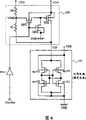
本发明第4实施例提供可有效降低内部电路中的泄漏电流,降低消耗电流的半导体集成电路。图4是本发明第4实施例的半导体集成电路的构成的等价电路图。The fourth embodiment of the present invention provides a semiconductor integrated circuit capable of effectively reducing leakage current in internal circuits and reducing current consumption. FIG. 4 is an equivalent circuit diagram showing the configuration of a semiconductor integrated circuit according to a fourth embodiment of the present invention.
(电路构成)(circuit configuration)
如图4所示,本发明第4实施例的半导体集成电路包含:内部电路100;在该内部电路100和接地GND之间电气连接,用于降低上述内部电路100待机时的泄漏电流的泄漏电流降低电路400。作为内部电路100的典型例可采用时序电路或者组合逻辑电路,但也不一定限于这些。作为时序电路的典型例可采用触发电路和锁存电路。以内部电路100由锁存电路100构成的场合为例进行以下说明。As shown in FIG. 4, the semiconductor integrated circuit of the fourth embodiment of the present invention includes: an
如图4所示,本发明第4实施例的半导体集成电路包含:锁存电路100;在该锁存电路100和接地GND之间电气连接,用于降低上述锁存电路100待机时的泄漏电流的泄漏电流降低电路400。该锁存电路100具有已知的电路构成。具体地说,如图4所示,锁存电路100由第1PMOS晶体管mp101、第2PMOS晶体管mp102、第1NMOS晶体管mn101、第2NMOS晶体管mn102构成。第1PMOS晶体管mp101的源极和第2PMOS晶体管mp102的源极与电源VDD连接。第1NMOS晶体管mn101的源极和第2NMOS晶体管mn102的源极与低电位侧端子VSN连接。第1PMOS晶体管mp101及第2PMOS晶体管mp102的基板电位由电源VDD保持。第1NMOS晶体管mn101及第2NMOS晶体管mn102的基板电位由接地GND保持。第1PMOS晶体管mp101的漏极和第1NMOS晶体管mn101的漏极相互连接,并且该漏极与第2PMOS晶体管mp102的栅极和第2NMOS晶体管mn102的栅极连接。第2PMOS晶体管mp102的漏极和第2NMOS晶体管mn102的漏极相互连接,并且该漏极与第1PMOS晶体管mp101的栅极和第1NMOS晶体管mn101的栅极连接。As shown in FIG. 4, the semiconductor integrated circuit of the fourth embodiment of the present invention includes: a
泄漏电流降低电路400与备用信号端子Standby连接,并与低电位侧端子VSN连接。该泄漏电流降低电路400由第1NMOS开关晶体管MS1、第3NMOS晶体管MN1、第3PMOS晶体管MP1、第1电阻R1和第2电阻R2串联构成的分压电路构成。第1NMOS开关晶体管MS1是连接到低电位侧端子VSN和接地GND之间,将低电位侧端子VSN与接地GND连接或从接地GND切断的开关元件。第3NMOS晶体管MN1及第3PMOS晶体管MP1以及第1电阻R1和第2电阻R2串联构成的分压电路,构成根据备用信号端子Standby控制第1NMOS开关晶体管MS1的开关动作的控制电路。The leakage current reducing circuit 400 is connected to the standby signal terminal Standby, and is also connected to the low potential side terminal VSN. The leakage current reducing circuit 400 is composed of a voltage dividing circuit composed of a first NMOS switching transistor MS1, a third NMOS transistor MN1, a third PMOS transistor MP1, a first resistor R1, and a second resistor R2 connected in series. The first NMOS switching transistor MS1 is a switching element connected between the low potential side terminal VSN and the ground GND, and connects the low potential side terminal VSN to the ground GND or disconnects it from the ground GND. A voltage divider circuit composed of the third NMOS transistor MN1, the third PMOS transistor MP1, and the first resistor R1 and the second resistor R2 in series constitutes a control circuit for controlling the switching operation of the first NMOS switching transistor MS1 according to the standby signal terminal Standby.
具体地说,如图4所示,第1NMOS开关晶体管MS1的源极与接地GND连接。第1NMOS开关晶体管MS1的漏极与低电位侧端子VSN连接。第1NMOS开关晶体管MS1的基板与接地GND连接。第1NMOS开关晶体管MS1的栅极与控制该第1NMOS开关晶体管MS1的开关动作的控制电路连接。该控制电路由第3NMOS晶体管MN1、第3PMOS晶体管MP1、第1电阻R1和第2电阻R2串联构成的分压电路构成。第1电阻R1和第2电阻R2串联构成的分压电路在低电位侧端子VSN和接地GND之间连接,由第1电阻R1和第2电阻R2之比确定的分压在第1电阻R1和第2电阻R2之间的节点VSM呈现。Specifically, as shown in FIG. 4 , the source of the first NMOS switching transistor MS1 is connected to the ground GND. The drain of the first NMOS switching transistor MS1 is connected to the low potential side terminal VSN. The substrate of the first NMOS switching transistor MS1 is connected to the ground GND. The gate of the first NMOS switching transistor MS1 is connected to a control circuit that controls the switching operation of the first NMOS switching transistor MS1. The control circuit is composed of a voltage divider circuit composed of a third NMOS transistor MN1, a third PMOS transistor MP1, a first resistor R1 and a second resistor R2 connected in series. A voltage dividing circuit composed of the first resistor R1 and the second resistor R2 connected in series is connected between the low potential side terminal VSN and the ground GND, and the divided voltage determined by the ratio of the first resistor R1 and the second resistor R2 is between the first resistor R1 and the second resistor R2. A node VSM is present between the second resistor R2.
第3NMOS晶体管MN1的源极与分压电路的节点VSM连接。换言之,第3NMOS晶体管MN1的源极经由第1电阻R1与低电位侧端子VSN连接,并经由第2电阻R2与接地GND连接。第3NMOS晶体管MN1的漏极与第1NMOS开关晶体管MS1的栅极连接。第3NMOS晶体管MN1的栅极与备用信号端子Standby连接。第3NMOS晶体管MN1的基板与接地GND连接。第3PMOS晶体管MP1的源极与电源VDD连接。第3PMOS晶体管MP1的漏极与第1NMOS开关晶体管MS1的栅极连接。第3PMOS晶体管MP1的栅极与备用信号端子Standby连接。第3PMOS晶体管MP1的基板与电源VDD连接。The source of the third NMOS transistor MN1 is connected to the node VSM of the voltage dividing circuit. In other words, the source of the third NMOS transistor MN1 is connected to the low potential side terminal VSN via the first resistor R1, and is connected to the ground GND via the second resistor R2. The drain of the third NMOS transistor MN1 is connected to the gate of the first NMOS switching transistor MS1. The gate of the third NMOS transistor MN1 is connected to the standby signal terminal Standby. The substrate of the third NMOS transistor MN1 is connected to the ground GND. The source of the third PMOS transistor MP1 is connected to the power supply VDD. The drain of the third PMOS transistor MP1 is connected to the gate of the first NMOS switching transistor MS1. The gate of the third PMOS transistor MP1 is connected to the standby signal terminal Standby. The substrate of the third PMOS transistor MP1 is connected to the power supply VDD.
第1NMOS开关晶体管MS1的尺寸即栅极宽度必须足够大,使得尽可能不影响动作时的内部电路100的特性,尽可能以低阻抗与接地GND连接,另外,为了兼顾布局面积和降低内部电路100的泄漏电流的效果,可采用适度的尺寸即栅极宽度。但是,第1NMOS开关晶体管MS1的尺寸有在动作时被内部电路的特性限制的情况。即,由于根据该尺寸和待机时的内部电路100的泄漏电流确定低电位侧端子VSN的电位,因此有难以设定成任意值的情况。因而如图4所示,通过设置在低电位侧端子VSN和接地GND之间插入的第1电阻R1及第2电阻R2串联构成的分压电路,用以第1电阻R1和第2电阻R2之比确定的分压比出现在节点VSM的电位来控制第1NMOS开关晶体管MS1的栅极电位。The size of the first NMOS switching transistor MS1, that is, the gate width must be large enough so that the characteristics of the
(电路动作)(circuit operation)
内部电路100动作时,从备用信号端子Standby输出低电平信号Low,第3NMOS晶体管MN1成为截止,第3PMOS晶体管MP1成为导通,第1NMOS开关晶体管MS1的栅极电位成为与电源VDD同一电平,第1NMOS开关晶体管MS1导通。从而,低电位侧端子VSN与接地GND以低阻抗连接,因此,内部电路100进行通常动作。When the
内部电路100待机时,从备用信号端子Standby输出高电平信号High,第3PMOS晶体管MP1成为截止,第3NMOS晶体管MN1成为导通,第1NMOS开关晶体管MS1的栅极与以第1电阻R1和第2电阻R2之比确定的分压比出现在节点VSM的电位连接。第1NMOS开关晶体管MS1,将待机时的内部电路100的泄漏电流作为偏置电流,以MOS二极管的方式动作,将低电位侧端子VSN的电位保持在比接地GND高的一恒电位。由于内部电路100的第1及第2NMOS晶体管mn101、mn102的基板电位与接地GND连接,通过源极-基板间的逆偏置效果,降低第1及第2NMOS晶体管mn101、mn102的泄漏电流。另外,由于通过对低电位侧端子VSN的偏置缓和电源VDD-接地GND间的电压差,因此通过电压缓和,第1及第2PMOS晶体管mp101、mp102的泄漏电流也被降低。When the
(效果)(Effect)
如上所述,根据本发明第4实施例,通过设置在低电位侧端子VSN和接地GND之间连接的第1电阻R1及第2电阻R2串联构成的分压电路,用以第1电阻R1和第2电阻R2之比确定的分压比出现在节点VSM的电位控制第1NMOS开关晶体管MS1的栅极电位。通过该构成调节第1电阻R1和第2电阻R2之比,可调节低电位侧端子VSN的电位。As described above, according to the fourth embodiment of the present invention, by providing a voltage divider circuit composed of the first resistor R1 and the second resistor R2 connected in series between the low potential side terminal VSN and the ground GND, the first resistor R1 and the second resistor R2 are connected in series. The voltage dividing ratio determined by the ratio of the second resistor R2 controls the potential of the gate of the first NMOS switching transistor MS1 by the potential appearing at the node VSM. By adjusting the ratio between the first resistor R1 and the second resistor R2 in this configuration, the potential of the low potential side terminal VSN can be adjusted.
另外,通过用第1电阻R1和第2电阻R2之比控制第1NMOS开关晶体管MS1的栅极电位,具有在内部电路100的泄漏电流大的条件下源极偏置电压变高而在泄漏电流小的条件下源极偏置电压变低的补正效果。泄漏电流小的条件是内部电路100的MOS晶体管的阈值电压大的条件,因此,成为待机时确保内部电路进行数据保持动作所必要的最低动作电压高的条件。因而,偏置电流小时,偏置电压小具有提高数据保持动作的抗噪声性的效果。In addition, by controlling the gate potential of the first NMOS switching transistor MS1 by using the ratio of the first resistor R1 to the second resistor R2, the source bias voltage becomes higher under the condition that the leakage current of the
(5)第5实施例(5) The fifth embodiment
本发明第5实施例提供可有效降低内部电路中的泄漏电流,降低消耗电流的半导体集成电路。图5是本发明第5实施例的半导体集成电路的构成的等价电路图。A fifth embodiment of the present invention provides a semiconductor integrated circuit capable of effectively reducing leakage current in internal circuits and reducing current consumption. Fig. 5 is an equivalent circuit diagram showing the configuration of a semiconductor integrated circuit according to a fifth embodiment of the present invention.
(电路构成)(circuit configuration)
如图5所示,本发明第5实施例的半导体集成电路包含:内部电路100;在该内部电路100和接地GND之间电气连接,用于降低上述内部电路100待机时的泄漏电流的泄漏电流降低电路500。作为内部电路100的典型例可采用时序电路或者组合逻辑电路,但也不一定限于这些。作为时序电路的典型例可采用触发电路和锁存电路。以内部电路100由锁存电路100构成的场合为例进行以下说明。As shown in FIG. 5, the semiconductor integrated circuit of the fifth embodiment of the present invention includes: an
如图5所示,本发明第5实施例的半导体集成电路包含:锁存电路100;在该锁存电路100和接地GND之间电气连接,用于降低上述锁存电路100待机时的泄漏电流的泄漏电流降低电路500。该锁存电路100具有已知的电路构成。具体地说,如图5所示,锁存电路100由第1PMOS晶体管mp101、第2PMOS晶体管mp102、第1NMOS晶体管mn101、第2NMOS晶体管mn102构成。第1PMOS晶体管mp101的源极和第2PMOS晶体管mp102的源极与电源VDD连接。第1NMOS晶体管mn101的源极和第2NMOS晶体管mn102的源极与低电位侧端子VSN连接。第1PMOS晶体管mp101及第2PMOS晶体管mp102的基板电位由电源VDD保持。第1NMOS晶体管mn101及第2NMOS晶体管mn102的基板电位由接地GND保持。第1PMOS晶体管mp101的漏极和第1NMOS晶体管mn101的漏极相互连接,并且该漏极与第2PMOS晶体管mp102的栅极和第2NMOS晶体管mn102的栅极连接。第2PMOS晶体管mp102的漏极和第2NMOS晶体管mn102的漏极相互连接,并且该漏极与第1PMOS晶体管mp101的栅极和第1NMOS晶体管mn101的栅极连接。As shown in FIG. 5, the semiconductor integrated circuit of the fifth embodiment of the present invention includes: a
泄漏电流降低电路500与备用信号端子Standby连接,并与低电位侧端子VSN连接。该泄漏电流降低电路500由第1NMOS开关晶体管MS1、第3NMOS晶体管MN1、第3PMOS晶体管MP1、常时导通状态的第5NMOS晶体管MR1和常时导通状态的第6NMOS晶体管MR2串联构成的分压电路构成。第1NMOS开关晶体管MS1是在低电位侧端子VSN和接地GND之间连接,将低电位侧端子VSN与接地GND连接或从接地GND切断的开关元件。第3NMOS晶体管MN1及第3PMOS晶体管MP1以及常时导通状态的第5NMOS晶体管MR1和常时导通状态的第6NMOS晶体管MR2串联构成的分压电路,构成根据备用信号端子Standby控制第1NMOS开关晶体管MS1的开关动作的控制电路。The leakage current reducing
具体地说,如图5所示,第1NMOS开关晶体管MS1的源极与接地GND连接。第1NMOS开关晶体管MS1的漏极与低电位侧端子VSN连接。第1NMOS开关晶体管MS1的基板与接地GND连接。第1NMOS开关晶体管MS1的栅极与控制该第1NMOS开关晶体管MS1的开关动作的控制电路连接。该控制电路由第3NMOS晶体管MN1、第3PMOS晶体管MP1、常时导通状态的第5NMOS晶体管MR1和常时导通状态的第6NMOS晶体管MR2串联构成的分压电路构成。常时导通状态的第5NMOS晶体管MR1和常时导通状态的第6NMOS晶体管MR2串联构成的分压电路,在低电位侧端子VSN和接地GND之间连接,以第5NMOS晶体管MR1的第1导通电阻和第6NMOS晶体管MR2的第2导通电阻之比确定的分压出现在第5NMOS晶体管MR1和第6NMOS晶体管MR2之间的节点VSM。这里,由于第5NMOS晶体管MR1保持常时导通状态,因此也可将第5NMOS晶体管MR1的栅极与电源VDD连接。同样,由于第6NMOS晶体管MR2保持常时导通状态,因此也可将第6NMOS晶体管MR2的栅极与电源VDD连接。Specifically, as shown in FIG. 5 , the source of the first NMOS switching transistor MS1 is connected to the ground GND. The drain of the first NMOS switching transistor MS1 is connected to the low potential side terminal VSN. The substrate of the first NMOS switching transistor MS1 is connected to the ground GND. The gate of the first NMOS switching transistor MS1 is connected to a control circuit that controls the switching operation of the first NMOS switching transistor MS1. The control circuit is composed of a voltage divider circuit composed of a third NMOS transistor MN1, a third PMOS transistor MP1, a fifth NMOS transistor MR1 in a normally on state, and a sixth NMOS transistor MR2 in a normally on state in series. The voltage divider circuit composed of the fifth NMOS transistor MR1 in the always-on state and the sixth NMOS transistor MR2 in the always-on state connected in series is connected between the low potential side terminal VSN and the ground GND, and the first lead of the fifth NMOS transistor MR1 A divided voltage determined by the ratio of the on-resistance to the second on-resistance of the sixth NMOS transistor MR2 appears at the node VSM between the fifth NMOS transistor MR1 and the sixth NMOS transistor MR2. Here, since the fifth NMOS transistor MR1 is always on, the gate of the fifth NMOS transistor MR1 may be connected to the power supply VDD. Similarly, since the sixth NMOS transistor MR2 is always on, the gate of the sixth NMOS transistor MR2 may also be connected to the power supply VDD.
第3NMOS晶体管MN1的源极与分压电路的节点VSM连接。换言之,第3NMOS晶体管MN1的源极经由第5NMOS晶体管MR1与低电位侧端子VSN连接,并经由第6NMOS晶体管MR2与接地GND连接。第3NMOS晶体管MN1的漏极与第1NMOS开关晶体管MS1的栅极连接。第3NMOS晶体管MN1的栅极与备用信号端子Standby连接。第3NMOS晶体管MN1的基板与接地GND连接。第3PMOS晶体管MP1的源极与电源VDD连接。第3PMOS晶体管MP1的漏极与第1NMOS开关晶体管MS1的栅极连接。第3PMOS晶体管MP1的栅极与备用信号端子Standby连接。第3PMOS晶体管MP1的基板与电源VDD连接。The source of the third NMOS transistor MN1 is connected to the node VSM of the voltage dividing circuit. In other words, the source of the third NMOS transistor MN1 is connected to the low-potential side terminal VSN through the fifth NMOS transistor MR1 , and is connected to the ground GND through the sixth NMOS transistor MR2 . The drain of the third NMOS transistor MN1 is connected to the gate of the first NMOS switching transistor MS1. The gate of the third NMOS transistor MN1 is connected to the standby signal terminal Standby. The substrate of the third NMOS transistor MN1 is connected to the ground GND. The source of the third PMOS transistor MP1 is connected to the power supply VDD. The drain of the third PMOS transistor MP1 is connected to the gate of the first NMOS switching transistor MS1. The gate of the third PMOS transistor MP1 is connected to the standby signal terminal Standby. The substrate of the third PMOS transistor MP1 is connected to the power supply VDD.
第1NMOS开关晶体管MS1的尺寸即栅极宽度必须足够大,使得尽可能不影响动作时的内部电路100的特性,尽可能以低阻抗与接地GND连接,另外,为了兼顾布局面积和降低内部电路100的泄漏电流的效果,可采用适度的尺寸即栅极宽度。但是,第1NMOS开关晶体管MS1的尺寸有在动作时被内部电路的特性限制的情况。即,由于根据该尺寸和待机时的内部电路100的泄漏电流确定低电位侧端子VSN的电位,因此有难以设定成任意值的情况。因而如图5所示,通过设置在低电位侧端子VSN和接地GND之间插入的常时导通状态的第5NMOS晶体管MR1和常时导通状态的第6NMOS晶体管MR2串联构成的分压电路,用以第5NMOS晶体管MR1的第1导通电阻和第6NMOS晶体管MR2的第2导通电阻之比确定的分压比出现在节点VSM的电位,控制第1NMOS开关晶体管MS1的栅极电位。The size of the first NMOS switching transistor MS1, that is, the gate width must be large enough so that the characteristics of the
(电路动作)(circuit operation)
内部电路100动作时,从备用信号端子Standby输出低电平信号Low,第3NMOS晶体管MN1成为截止,第3PMOS晶体管MP1成为导通,第1NMOS开关晶体管MS1的栅极电位成为与电源VDD同一电平,第1NMOS开关晶体管MS1导通。从而,低电位侧端子VSN与接地GND以低阻抗连接,因此内部电路100进行通常动作。When the
内部电路100待机时,从备用信号端子Standby输出高电平信号High,第3PMOS晶体管MP1成为截止,第3NMOS晶体管MN1成为导通,第1NMOS开关晶体管MS1的栅极连接到以第5NMOS晶体管MR1的第1导通电阻和第6NMOS晶体管MR2的第2导通电阻之比确定的分压比出现在节点VSM的电位。第1NMOS开关晶体管MS1,将待机时的内部电路100的泄漏电流作为偏置电流,以MOS二极管的方式动作,将低电位侧端子VSN的电位保持在比接地GND高的一恒电位。由于内部电路100的第1及第2NMOS晶体管mn101、mn102的基板电位与接地GND连接,通过源极-基板间的逆偏置效果,降低第1及第2NMOS晶体管mn101、mn102的泄漏电流。另外,通过对低电位侧端子VSN的偏置缓和电源VDD-接地GND间的电压差,因此通过电压缓和,第1及第2PMOS晶体管mp101、mp102的泄漏电流也被降低。When the
(效果)(Effect)
如上所述,根据本发明第5实施例,通过设置在低电位侧端子VSN和接地GND之间连接的常时导通状态的第5NMOS晶体管MR1和常时导通状态的第6NMOS晶体管MR2串联构成的分压电路,用以第1导通电阻和第2导通电阻之比确定的分压比出现在节点VSM的电位来控制第1NMOS开关晶体管MS1的栅极电位。通过该构成来调节第1导通电阻和第2导通电阻之比,可调节低电位侧端子VSN的电位。As described above, according to the fifth embodiment of the present invention, the fifth NMOS transistor MR1 in the always-on state and the sixth NMOS transistor MR2 in the always-on state connected in series between the low potential side terminal VSN and the ground GND are configured in series. The voltage dividing circuit controls the gate potential of the first NMOS switching transistor MS1 by using the potential appearing at the node VSM at a voltage dividing ratio determined by the ratio of the first on-resistance to the second on-resistance. By adjusting the ratio of the first on-resistance to the second on-resistance in this configuration, the potential of the low-potential-side terminal VSN can be adjusted.
另外,通过用第1导通电阻和第2导通电阻之比控制第1NMOS开关晶体管MS1的栅极电位,具有在内部电路100的泄漏电流大的条件下源极偏置电压变高而在泄漏电流小的条件下源极偏置电压变低的补正效果。泄漏电流小的条件是内部电路100的MOS晶体管的阈值电压大的条件,因此,成为待机时确保内部电路进行数据保持动作所必要的最低动作电压高的条件。因而,偏置电流小时,偏置电压小具有提高数据保持动作的抗噪声性的效果。In addition, by controlling the gate potential of the first NMOS switching transistor MS1 by using the ratio of the first on-resistance to the second on-resistance, the source bias voltage becomes higher under the condition that the leakage current of the
(6)第6实施例(6) The sixth embodiment
本发明第6实施例提供可有效降低内部电路中的泄漏电流,降低消耗电流的半导体集成电路。图6是本发明第6实施例的半导体集成电路的构成的等价电路图。The sixth embodiment of the present invention provides a semiconductor integrated circuit capable of effectively reducing leakage current in internal circuits and reducing current consumption. FIG. 6 is an equivalent circuit diagram showing the configuration of a semiconductor integrated circuit according to a sixth embodiment of the present invention.
(电路构成)(circuit configuration)
如图6所示,本发明第6实施例的半导体集成电路包含:内部电路100;在该内部电路100和电源VDD之间电气连接,用于降低上述内部电路100待机时的泄漏电流的泄漏电流降低电路600。作为内部电路100的典型例可采用时序电路或者组合逻辑电路,但也不一定限于这些。作为时序电路的典型例可采用触发电路和锁存电路。以内部电路100由锁存电路100构成的场合为例进行以下说明。As shown in FIG. 6 , the semiconductor integrated circuit of the sixth embodiment of the present invention includes: an
如图6所示,本发明第6实施例的半导体集成电路包含:锁存电路100;在该锁存电路100和电源VDD之间电气连接,用于降低上述锁存电路100待机时的泄漏电流的泄漏电流降低电路600。该锁存电路100具有已知的电路构成。具体地说,如图6所示,锁存电路100由第1PMOS晶体管mp101、第2PMOS晶体管mp102、第1NMOS晶体管mn101、第2NMOS晶体管mn102构成。第1PMOS晶体管mp101的源极和第2PMOS晶体管mp102的源极与高电位侧端子VSP连接。第1NMOS晶体管mn101的源极和第2NMOS晶体管mn102的源极与接地GND连接。第1PMOS晶体管mp101及第2PMOS晶体管mp102的基板电位由电源VDD保持。第1NMOS晶体管mn101及第2NMOS晶体管mn102的基板电位由接地GND保持。第1PMOS晶体管mp101的漏极和第1NMOS晶体管mn101的漏极相互连接,并且该漏极与第2PMOS晶体管mp102的栅极和第2NMOS晶体管mn102的栅极连接。第2PMOS晶体管mp102的漏极和第2NMOS晶体管mn102的漏极相互连接,并且该漏极与第1PMOS晶体管mp101的栅极和第1NMOS晶体管mn101的栅极连接。As shown in FIG. 6, the semiconductor integrated circuit of the sixth embodiment of the present invention includes: a
泄漏电流降低电路600经由反相器INV1与备用信号端子Standby连接,并与高电位侧端子VSP连接。该泄漏电流降低电路600由第2PMOS开关晶体管MS2、第4NMOS晶体管MN2、第4PMOS晶体管MP2、第3电阻R3和第4电阻R4的串联构成的分压电路构成。第2PMOS开关晶体管MS2是在高电位侧端子VSP和电源VDD之间连接,将高电位侧端子VSP与电源VDD连接或从电源VDD切断的开关元件。第4NMOS晶体管MN2及第4PMOS晶体管MP2以及第3电阻R3和第4电阻R4串联构成的分压电路,构成根据备用信号端子Standby的反相信号来控制第2PMOS开关晶体管MS2的开关动作的控制电路。The leakage current reducing
具体地说,如图6所示,第2PMOS开关晶体管MS2的源极与电源VDD连接。第2PMOS开关晶体管MS2的漏极与高电位侧端子VSP连接。第2PMOS开关晶体管MS2的基板与电源VDD连接。第2PMOS开关晶体管MS2的栅极与控制第2PMOS开关晶体管MS2的开关动作的控制电路连接。该控制电路由第4NMOS晶体管MN2、第4PMOS晶体管MP2、第3电阻R3和第4电阻R4串联构成的分压电路构成。第3电阻R3及第4电阻R4串联构成的分压电路在高电位侧端子VSP和电源VDD之间连接,由第3电阻R3和第4电阻R4之比确定的分压出现在第3电阻R3和第4电阻R4之间的节点VSM2。Specifically, as shown in FIG. 6, the source of the second PMOS switching transistor MS2 is connected to the power supply VDD. The drain of the second PMOS switching transistor MS2 is connected to the high potential side terminal VSP. The substrate of the second PMOS switching transistor MS2 is connected to the power supply VDD. The gate of the second PMOS switching transistor MS2 is connected to a control circuit that controls the switching operation of the second PMOS switching transistor MS2. The control circuit is composed of a voltage divider circuit composed of a fourth NMOS transistor MN2, a fourth PMOS transistor MP2, a third resistor R3 and a fourth resistor R4 connected in series. The voltage divider circuit composed of the third resistor R3 and the fourth resistor R4 connected in series is connected between the high potential side terminal VSP and the power supply VDD, and the divided voltage determined by the ratio between the third resistor R3 and the fourth resistor R4 appears in the third resistor R3 and the node VSM2 between the fourth resistor R4.
第4PMOS晶体管MP2的源极与分压电路的节点VSM2连接。换言之,第4PMOS晶体管MP2的源极经由第3电阻R3与高电位侧端子VSP连接,并经由第4电阻R4与电源VDD连接。第4PMOS晶体管MP2的漏极与第2PMOS开关晶体管MS2的栅极连接。第4PMOS晶体管MP2的栅极经由反相器INV1与备用信号端子Standby连接。第4PMOS晶体管MP2的基板与电源VDD连接。第4NMOS晶体管MN2的源极与接地GND连接。第4NMOS晶体管MN2的漏极与第2PMOS开关晶体管MS2的栅极连接。第4NMOS晶体管MN2的栅极经由反相器INV1与备用信号端子Standby连接。第4NMOS晶体管MN2的基板与接地GND连接。The source of the fourth PMOS transistor MP2 is connected to the node VSM2 of the voltage dividing circuit. In other words, the source of the fourth PMOS transistor MP2 is connected to the high potential side terminal VSP via the third resistor R3, and is connected to the power supply VDD via the fourth resistor R4. The drain of the fourth PMOS transistor MP2 is connected to the gate of the second PMOS switching transistor MS2. The gate of the fourth PMOS transistor MP2 is connected to the standby signal terminal Standby via the inverter INV1. The substrate of the fourth PMOS transistor MP2 is connected to the power supply VDD. The source of the fourth NMOS transistor MN2 is connected to the ground GND. The drain of the fourth NMOS transistor MN2 is connected to the gate of the second PMOS switching transistor MS2. The gate of the fourth NMOS transistor MN2 is connected to the standby signal terminal Standby via the inverter INV1. The substrate of the fourth NMOS transistor MN2 is connected to the ground GND.
第2PMOS开关晶体管MS2的尺寸即栅极宽度必须足够大,使得尽可能不影响动作时的内部电路100的特性,尽可能以低阻抗与电源VDD连接,另外,为了兼顾布局面积和降低内部电路100的泄漏电流的效果,可采用适度的尺寸即栅极宽度。但是,第2PMOS开关晶体管MS2的尺寸有在动作时被内部电路的特性限制的情况。即,由于根据该尺寸和待机时的内部电路100的泄漏电流确定高电位侧端子VSP的电位,因此有难以设定成任意值的情况。因而如图6所示,通过设置在高电位侧端子VSP和电源VDD之间插入的第3电阻R3及第4电阻R4串联构成的分压电路,用以第3电阻R3和第4电阻R4之比确定的分压比出现在节点VSM2的电位,控制第2PMOS开关晶体管MS2的栅极电位。The size of the second PMOS switching transistor MS2, that is, the gate width must be large enough so that the characteristics of the
(电路动作)(circuit operation)
内部电路100动作时,从备用信号端子Standby输出低电平信号Low,该备用信号端子Standby的反相信号即高电平信号High输入泄漏电流降低电路600。其结果,第4NMOS晶体管MN2成为导通,第4PMOS晶体管MP2成为截止,第2PMOS开关晶体管MS2的栅极电位成为与接地GND同一电平,第2PMOS开关晶体管MS2导通。从而,高电位侧端子VSP与电源VDD以低阻抗连接,因此内部电路100进行通常动作。When the
内部电路100待机时,从备用信号端子Standby输出高电平信号High,该备用信号端子Standby的反相信号即低电平信号Low输入泄漏电流降低电路600。第4PMOS晶体管MP2成为导通,第4NMOS晶体管MN2成为截止,第2PMOS开关晶体管MS2的栅极与第3电阻R3和第4电阻R4之比确定的分压比出现在节点VSM2的电位连接。第2PMOS开关晶体管MS2将待机时的内部电路100的泄漏电流作为偏置电流,以MOS二极管的方式动作,将高电位侧端子VSP的电位保持在比电源VDD低的一恒电位。由于内部电路100的第1及第2PMOS晶体管mp101、mp102的基板电位与电源VDD连接,通过源极-基板间的逆偏置效果,降低第1及第2PMOS晶体管mp101、mp102的泄漏电流。另外,通过对高电位侧端子VSP的偏置缓和电源VDD-接地GND间的电压差,因此通过电压缓和,第1及第2NMOS晶体管mn101、mn102的泄漏电流也被降低。When the
(效果)(Effect)
如上所述,根据本发明第6实施例,通过设置在高电位侧端子VSP和电源VDD之间连接的第3电阻R3及第4电阻R4串联构成的分压电路,用以第3电阻R3和第4电阻R4之比确定的分压比出现在节点VSM2的电位,控制第2PMOS开关晶体管MS2的栅极电位。通过采用该构成调节第3电阻R3和第4电阻R4之比,可调节高电位侧端子VSP的电位。As described above, according to the sixth embodiment of the present invention, by providing a voltage divider circuit composed of the third resistor R3 and the fourth resistor R4 connected in series between the high potential side terminal VSP and the power supply VDD, the third resistor R3 and the fourth resistor R4 are connected in series. The voltage division ratio determined by the ratio of the fourth resistor R4 appears at the potential of the node VSM2 to control the gate potential of the second PMOS switching transistor MS2. By adjusting the ratio of the third resistor R3 and the fourth resistor R4 with this configuration, the potential of the high potential side terminal VSP can be adjusted.
另外,通过用第3电阻R3和第4电阻R4之比控制第2PMOS开关晶体管MS2的栅极电位,具有在内部电路100的泄漏电流大的条件下源极偏置电压变高而在泄漏电流小的条件下源极偏置电压变低的补正效果。泄漏电流小的条件是内部电路100的MOS晶体管的阈值电压大的条件,因此,成为待机时确保内部电路进行数据保持动作所必要的最低动作电压高的条件。因而,偏置电流小时,偏置电压小具有提高数据保持动作的抗噪声性的效果。In addition, by controlling the gate potential of the second PMOS switching transistor MS2 by using the ratio between the third resistor R3 and the fourth resistor R4, the source bias voltage becomes high under the condition that the leakage current of the
(7)第7实施例(7) The seventh embodiment
本发明第7实施例提供可有效降低内部电路中的泄漏电流,降低消耗电流的半导体集成电路。图7是本发明第7实施例的半导体集成电路的构成的等价电路图。A seventh embodiment of the present invention provides a semiconductor integrated circuit capable of effectively reducing leakage current in internal circuits and reducing current consumption. Fig. 7 is an equivalent circuit diagram showing the structure of a semiconductor integrated circuit according to a seventh embodiment of the present invention.
(电路构成)(circuit configuration)
如图7所示,本发明第7实施例的半导体集成电路包含:内部电路100;在该内部电路100和电源VDD之间电气连接,用于降低上述内部电路100待机时的泄漏电流的泄漏电流降低电路700。作为内部电路100的典型例可采用时序电路或者组合逻辑电路,但也不一定限于这些。作为时序电路的典型例可采用触发电路和锁存电路。以内部电路100由锁存电路100构成的场合为例进行以下说明。As shown in FIG. 7 , the semiconductor integrated circuit of the seventh embodiment of the present invention includes: an
如图7所示,本发明第7实施例的半导体集成电路包含:锁存电路100;在该锁存电路100和电源VDD之间电气连接,用于降低上述锁存电路100待机时的泄漏电流的泄漏电流降低电路700。该锁存电路100具有已知的电路构成。具体地说,如图7所示,锁存电路100由第1PMOS晶体管mp101、第2PMOS晶体管mp102、第1NMOS晶体管mn101、第2NMOS晶体管mn102构成。第1PMOS晶体管mp101的源极和第2PMOS晶体管mp102的源极与高电位侧端子VSP连接。第1NMOS晶体管mn101的源极和第2NMOS晶体管mn102的源极与接地GND连接。第1PMOS晶体管mp101及第2PMOS晶体管mp102的基板电位由电源VDD保持。第1NMOS晶体管mn101及第2NMOS晶体管mn102的基板电位由接地GND保持。第1PMOS晶体管mp101的漏极和第1NMOS晶体管mn101的漏极相互连接,并且该漏极与第2PMOS晶体管mp102的栅极和第2NMOS晶体管mn102的栅极连接。第2PMOS晶体管mp102的漏极和第2NMOS晶体管mn102的漏极相互连接,并且该漏极与第1PMOS晶体管mp101的栅极和第1NMOS晶体管mn101的栅极连接。As shown in FIG. 7, the semiconductor integrated circuit of the seventh embodiment of the present invention includes: a
泄漏电流降低电路700经由反相器INV1与备用信号端子Standby连接,并与高电位侧端子VSP连接。该泄漏电流降低电路700由第2PMOS开关晶体管MS2、第4NMOS晶体管MN2、第4PMOS晶体管MP2、常时导通状态的第5PMOS晶体管MR3和常时导通状态的第6PMOS晶体管MR4串联构成的分压电路构成。第2PMOS开关晶体管MS2是在高电位侧端子VSP和电源VDD之间连接,将高电位侧端子VSP与电源VDD连接或从电源VDD切断的开关元件。第4NMOS晶体管MN2及第4PMOS晶体管MP2以及常时导通状态的第5PMOS晶体管MR3和常时导通状态的第6PMOS晶体管MR4串联构成的分压电路,构成根据备用信号端子Standby的反相信号来控制第2PMOS开关晶体管MS2的开关动作的控制电路。The leakage current reducing
具体地说,如图7所示,第2PMOS开关晶体管MS2的源极与电源VDD连接。第2PMOS开关晶体管MS2的漏极与高电位侧端子VSP连接。第2PMOS开关晶体管MS2的基板与电源VDD连接。第2PMOS开关晶体管MS2的栅极与控制第2PMOS开关晶体管MS2的开关动作的控制电路连接。该控制电路由第4NMOS晶体管MN2、第4PMOS晶体管MP2、常时导通状态的第5PMOS晶体管MR3和常时导通状态的第6PMOS晶体管MR4串联构成的分压电路构成。常时导通状态的第5PMOS晶体管MR 3和常时导通状态的第6PMOS晶体管MR4串联构成的分压电路在高电位侧端子VSP和电源VDD之间连接,以第5PMOS晶体管MR3的第3导通电阻和第6PMOS晶体管MR4的第4导通电阻之比确定的分压出现在第5PMOS晶体管MR3和第6PMOS晶体管MR4之间的节点VSM2。这里,为了将第5PMOS晶体管MR3保持在常时导通状态,也可将第5PMOS晶体管MR3的栅极与接地GND连接。同样,为了将第6PMOS晶体管MR4保持在常时导通状态,也可将第6PMOS晶体管MR4的栅极与接地GND连接。Specifically, as shown in FIG. 7, the source of the second PMOS switching transistor MS2 is connected to the power supply VDD. The drain of the second PMOS switching transistor MS2 is connected to the high potential side terminal VSP. The substrate of the second PMOS switching transistor MS2 is connected to the power supply VDD. The gate of the second PMOS switching transistor MS2 is connected to a control circuit that controls the switching operation of the second PMOS switching transistor MS2. The control circuit is composed of a voltage divider circuit composed of a fourth NMOS transistor MN2, a fourth PMOS transistor MP2, a fifth PMOS transistor MR3 in a normally on state, and a sixth PMOS transistor MR4 in a normally on state in series. The voltage divider circuit composed of the fifth PMOS transistor MR3 in the always-on state and the sixth PMOS transistor MR4 in the always-on state connected in series is connected between the high potential side terminal VSP and the power supply VDD, and the third lead of the fifth PMOS transistor MR3 A divided voltage determined by the ratio of the on-resistance to the fourth on-resistance of the sixth PMOS transistor MR4 appears at the node VSM2 between the fifth PMOS transistor MR3 and the sixth PMOS transistor MR4. Here, in order to keep the fifth PMOS transistor MR3 in the always-on state, the gate of the fifth PMOS transistor MR3 may be connected to the ground GND. Similarly, in order to keep the sixth PMOS transistor MR4 in the always-on state, the gate of the sixth PMOS transistor MR4 may be connected to the ground GND.
第4PMOS晶体管MP2的源极与分压电路的节点VSM2连接。换言之,第4PMOS晶体管MP2的源极经由第6PMOS晶体管MR4与高电位侧端子VSP连接,并经由第5PMOS晶体管MR3与电源VDD连接。第4PMOS晶体管MP2的漏极与第2PMOS开关晶体管MS2的栅极连接。第4PMOS晶体管MP2的栅极经由反相器INV1与备用信号端子Standby连接。第4PMOS晶体管MP2的基板与电源VDD连接。第4NMOS晶体管MN2的源极与接地GND连接。第4NMOS晶体管MN2的漏极与第2PMOS开关晶体管MS2的栅极连接。第4NMOS晶体管MN2的栅极经由反相器INV1与备用信号端子Standby连接。第4NMOS晶体管MN2的基板与接地GND连接。The source of the fourth PMOS transistor MP2 is connected to the node VSM2 of the voltage dividing circuit. In other words, the source of the fourth PMOS transistor MP2 is connected to the high-potential-side terminal VSP via the sixth PMOS transistor MR4 , and is connected to the power supply VDD via the fifth PMOS transistor MR3 . The drain of the fourth PMOS transistor MP2 is connected to the gate of the second PMOS switching transistor MS2. The gate of the fourth PMOS transistor MP2 is connected to the standby signal terminal Standby via the inverter INV1. The substrate of the fourth PMOS transistor MP2 is connected to the power supply VDD. The source of the fourth NMOS transistor MN2 is connected to the ground GND. The drain of the fourth NMOS transistor MN2 is connected to the gate of the second PMOS switching transistor MS2. The gate of the fourth NMOS transistor MN2 is connected to the standby signal terminal Standby via the inverter INV1. The substrate of the fourth NMOS transistor MN2 is connected to the ground GND.
第2PMOS开关晶体管MS2的尺寸即栅极宽度必须足够大,使得尽可能不影响动作时的内部电路100的特性,尽可能以低阻抗与电源VDD连接,另外,为了兼顾布局面积和降低内部电路100的泄漏电流的效果,可采用适度的尺寸即栅极宽度。但是,第2PMOS开关晶体管MS2的尺寸有在动作时被内部电路的特性限制的情况。即,由于根据该尺寸和待机时的内部电路100的泄漏电流确定高电位侧端子VSP的电位,因此有难以设定成任意值的情况。因而如图7所示,通过设置在高电位侧端子VSP和电源VDD之间插入的常时导通状态的第5PMOS晶体管MR3和常时导通状态的第6PMOS晶体管MR4串联构成的分压电路,用以第3导通电阻和第4导通电阻之比确定的分压比出现在节点VSM2的电位来控制第2PMOS开关晶体管MS2的栅极电位。The size of the second PMOS switching transistor MS2, that is, the gate width must be large enough so that the characteristics of the
(电路动作)(circuit operation)
内部电路100动作时,从备用信号端子Standby输出低电平信号Low,该备用信号端子Standby的反相信号即高电平信号High输入泄漏电流降低电路700。其结果,第4NMOS晶体管MN2成为导通,第4PMOS晶体管MP2成为截止,第2PMOS开关晶体管MS2的栅极电位成为与接地GND同一电平,第2PMOS开关晶体管MS2导通。从而,高电位侧端子VSP与电源VDD以低阻抗连接,因此内部电路100进行通常动作。When the
内部电路100待机时,从备用信号端子Standby输出高电平信号High,该备用信号端子Standby的反相信号即低电平信号Low输入泄漏电流降低电路700。第4PMOS晶体管MP2成为导通,第4NMOS晶体管MN2成为截止,第2PMOS开关晶体管MS2的栅极与以第3导通电阻和第4导通电阻之比确定的分压比出现在节点VSM2的电位连接。第2PMOS开关晶体管MS2,将待机时的内部电路100的泄漏电流作为偏置电流,以MOS二极管的方式动作,将高电位侧端子VSP的电位保持在比电源VDD低的一恒电位。由于内部电路100的第1及第2PMOS晶体管mp101、mp102的基板电位与电源VDD连接,通过源极-基板间的逆偏置效果,降低第1及第2PMOS晶体管mp101、mp102的泄漏电流。另外,通过对高电位侧端子VSP的偏置缓和电源VDD-接地GND间的电压差,因此通过电压缓和,第1及第2NMOS晶体管mn101、mn102的泄漏电流也被降低。When the
(效果)(Effect)
如上所述,根据本发明第7实施例,通过设置在高电位侧端子VSP和电源VDD之间连接的第5PMOS晶体管MR3和第6PMOS晶体管MR4串联构成的分压电路,用以第3导通电阻和第4导通电阻之比确定的分压比出现在节点VSM2的电位控制第2PMOS开关晶体管MS2的栅极电位。通过采用该构成调节第3导通电阻和第4导通电阻之比,可调节高电位侧端子VSP的电位。As described above, according to the seventh embodiment of the present invention, by providing a voltage dividing circuit composed of the fifth PMOS transistor MR3 and the sixth PMOS transistor MR4 connected in series between the high potential side terminal VSP and the power supply VDD, the third on-resistance The voltage division ratio determined by the ratio of the fourth on-resistance appears at the node VSM2 to control the gate potential of the second PMOS switching transistor MS2. By adjusting the ratio of the third on-resistance to the fourth on-resistance in this configuration, the potential of the high-potential-side terminal VSP can be adjusted.
另外,通过用第3导通电阻R3和第4导通电阻R4之比控制第2PMOS开关晶体管MS2的栅极电位,具有在内部电路100的泄漏电流大的条件下源极偏置电压变高而在泄漏电流小的条件下源极偏置电压变低的补正效果。泄漏电流小的条件是内部电路100的MOS晶体管的阈值电压大的条件,因此,成为待机时确保内部电路进行数据保持动作所必要的最低动作电压高的条件。因而,偏置电流小时,偏置电压小具有提高数据保持动作的抗噪声性的效果。In addition, by controlling the gate potential of the second PMOS switching transistor MS2 by using the ratio of the third on-resistance R3 to the fourth on-resistance R4, the source bias voltage becomes higher under the condition that the leakage current of the
(8)第8实施例(8) Eighth embodiment
本发明第8实施例提供可有效降低内部电路中的泄漏电流,降低消耗电流的半导体集成电路。图8是本发明第8实施例的半导体集成电路的构成的等价电路图。An eighth embodiment of the present invention provides a semiconductor integrated circuit capable of effectively reducing leakage current in internal circuits and reducing current consumption. Fig. 8 is an equivalent circuit diagram showing the configuration of a semiconductor integrated circuit according to an eighth embodiment of the present invention.
(电路构成)(circuit configuration)
如图8所示,本发明第8实施例的半导体集成电路包含:内部电路100;在该内部电路100和接地GND之间电气连接,用于降低上述内部电路100待机时的泄漏电流的泄漏电流降低电路400;在该内部电路100和电源VDD之间电气连接,用于降低上述内部电路100待机时的泄漏电流的泄漏电流降低电路600。作为内部电路100的典型例可采用时序电路或者组合逻辑电路,但也不一定限于这些。作为时序电路的典型例可采用触发电路和锁存电路。以内部电路100由锁存电路100构成的场合为例进行以下说明。As shown in FIG. 8, the semiconductor integrated circuit of the eighth embodiment of the present invention includes: an
如图8所示,本发明第8实施例的半导体集成电路包含:锁存电路100;在该锁存电路100和接地GND之间电气连接,用于降低上述锁存电路100待机时的泄漏电流的泄漏电流降低电路400;在该内部电路100和电源VDD之间电气连接,用于降低上述内部电路100待机时的泄漏电流的泄漏电流降低电路600。该锁存电路100具有已知的电路构成。具体地说,如图8所示,锁存电路100由第1PMOS晶体管mp101、第2PMOS晶体管mp102、第1NMOS晶体管mn101、第2NMOS晶体管mn102构成。第1PMOS晶体管mp101的源极和第2PMOS晶体管mp102的源极与高电位侧端子VSP连接。第1NMOS晶体管mn101的源极和第2NMOS晶体管mn102的源极与低电位侧端子VSN连接。第1PMOS晶体管mp101及第2PMOS晶体管mp102的基板电位由电源VDD保持。第1NMOS晶体管mn101及第2NMOS晶体管mn102的基板电位由接地GND保持。第1PMOS晶体管mp101的漏极和第1NMOS晶体管mn101的漏极相互连接,并且该漏极与第2PMOS晶体管mp102的栅极和第2NMOS晶体管mn102的栅极连接。第2PMOS晶体管mp102的漏极和第2NMOS晶体管mn102的漏极相互连接,并且该漏极与第1NMOS晶体管mp101的栅极和第1NMOS晶体管mn101的栅极连接。As shown in FIG. 8, the semiconductor integrated circuit of the eighth embodiment of the present invention includes: a
泄漏电流降低电路400与备用信号端子Standby连接,并与低电位侧端子VSN连接。该泄漏电流降低电路400由第1NMOS开关晶体管MS1、第3NMOS晶体管MN1、第3PMOS晶体管MP1、第1电阻R1和第2电阻R2串联构成的分压电路构成。第1NMOS开关晶体管MS1是在低电位侧端子VSN和接地GND之间连接,将低电位侧端子VSN与接地GND连接或从接地GND切断的开关元件。第3NMOS晶体管MN1及第3PMOS晶体管MP1以及第1电阻R1和第2电阻R2串联构成的分压电路,构成根据备用信号端子Standby来控制第1NMOS开关晶体管MS1的开关动作的控制电路。The leakage current reducing circuit 400 is connected to the standby signal terminal Standby, and is also connected to the low potential side terminal VSN. The leakage current reducing circuit 400 is composed of a voltage dividing circuit composed of a first NMOS switching transistor MS1, a third NMOS transistor MN1, a third PMOS transistor MP1, a first resistor R1, and a second resistor R2 connected in series. The first NMOS switching transistor MS1 is a switching element connected between the low potential side terminal VSN and the ground GND, and is connected to or disconnected from the low potential side terminal VSN to the ground GND. The voltage divider circuit composed of the third NMOS transistor MN1, the third PMOS transistor MP1, and the first resistor R1 and the second resistor R2 in series constitutes a control circuit for controlling the switching operation of the first NMOS switching transistor MS1 according to the standby signal terminal Standby.
具体地说,如图8所示,第1NMOS开关晶体管MS1的源极与接地GND连接。第1NMOS开关晶体管MS1的漏极与低电位侧端子VSN连接。第1NMOS开关晶体管MS1的基板与接地GND连接。第1NMOS开关晶体管MS1的栅极与控制该第1NMOS开关晶体管MS1的开关动作的控制电路连接。该控制电路由第3NMOS晶体管MN1、第3PMOS晶体管MP1、第1电阻R1和第2电阻R2串联构成的分压电路构成。第1电阻R1及第2电阻R2串联构成的分压电路在低电位侧端子VSN和接地GND之间连接,以第1电阻R1和第2电阻R2之比确定的分压出现在第1电阻R1和第2电阻R2之间的节点VSM。Specifically, as shown in FIG. 8 , the source of the first NMOS switching transistor MS1 is connected to the ground GND. The drain of the first NMOS switching transistor MS1 is connected to the low potential side terminal VSN. The substrate of the first NMOS switching transistor MS1 is connected to the ground GND. The gate of the first NMOS switching transistor MS1 is connected to a control circuit that controls the switching operation of the first NMOS switching transistor MS1. The control circuit is composed of a voltage divider circuit composed of a third NMOS transistor MN1, a third PMOS transistor MP1, a first resistor R1 and a second resistor R2 connected in series. The voltage divider circuit composed of the first resistor R1 and the second resistor R2 connected in series is connected between the low potential side terminal VSN and the ground GND, and the divided voltage determined by the ratio of the first resistor R1 and the second resistor R2 appears in the first resistor R1 and the node VSM between the second resistor R2.
第3NMOS晶体管MN1的源极与分压电路的节点VSM连接。换言之,第3NMOS晶体管MN1的源极经由第1电阻R1与低电位侧端子VSN连接,并经由第2电阻R2与接地GND连接。第3NMOS晶体管MN1的漏极与第1NMOS开关晶体管MS1的栅极连接。第3NMOS晶体管MN1的栅极与备用信号端子Standby连接。第3NMOS晶体管MN1的基板与接地GND连接。第3PMOS晶体管MP1的源极与电源VDD连接。第3PMOS晶体管MP1的漏极与第1NMOS开关晶体管MS1的栅极连接。第3PMOS晶体管MP1的栅极与备用信号端子Standby连接。第3PMOS晶体管MP1的基板与电源VDD连接。The source of the third NMOS transistor MN1 is connected to the node VSM of the voltage dividing circuit. In other words, the source of the third NMOS transistor MN1 is connected to the low potential side terminal VSN via the first resistor R1, and is connected to the ground GND via the second resistor R2. The drain of the third NMOS transistor MN1 is connected to the gate of the first NMOS switching transistor MS1. The gate of the third NMOS transistor MN1 is connected to the standby signal terminal Standby. The substrate of the third NMOS transistor MN1 is connected to the ground GND. The source of the third PMOS transistor MP1 is connected to the power supply VDD. The drain of the third PMOS transistor MP1 is connected to the gate of the first NMOS switching transistor MS1. The gate of the third PMOS transistor MP1 is connected to the standby signal terminal Standby. The substrate of the third PMOS transistor MP1 is connected to the power supply VDD.
第1NMOS开关晶体管MS1的尺寸即栅极宽度必须足够大,使得尽可能不影响动作时的内部电路100的特性,尽可能以低阻抗与接地GND连接,另外,为了兼顾布局面积和降低内部电路100的泄漏电流的效果,可采用适度的尺寸即栅极宽度。但是,第1NMOS开关晶体管MS1的尺寸有在动作时被内部电路的特性限制的情况。即,由于根据该尺寸和待机时的内部电路100的泄漏电流确定低电位侧端子VSN的电位,因此有难以设定成任意值的情况。因而如图8所示,通过设置在低电位侧端子VSN和接地GND之间插入的第1电阻R1和第2电阻R2串联构成的分压电路,用以第1电阻R1和第2电阻R2之比确定的分压比出现在节点VSM的电位控制第1NMOS开关晶体管MS1的栅极电位。The size of the first NMOS switching transistor MS1, that is, the gate width must be large enough so that the characteristics of the
泄漏电流降低电路600经由反相器INV1与备用信号端子Standby连接,并与高电位侧端子VSP连接。该泄漏电流降低电路600由第2PMOS开关晶体管MS2、第4NMOS晶体管MN2、第4PMOS晶体管MP2、第3电阻R3及第4电阻R4串联构成的分压电路构成。第2PMOS开关晶体管MS2是在高电位侧端子VSP和电源VDD之间连接,将高电位侧端子VSP与电源VDD连接或从电源VDD切断的开关元件。第4NMOS晶体管MN2及第4PMOS晶体管MP2以及第3电阻R3和第4电阻R4串联构成的分压电路,构成根据备用信号端子Standby的反相信号来控制第2PMOS开关晶体管MS2的开关动作的控制电路。The leakage current reducing
具体地说,如图8所示,第2PMOS开关晶体管MS2的源极与电源VDD连接。第2PMOS开关晶体管MS2的漏极与高电位侧端子VSP连接。第2PMOS开关晶体管MS2的基板与电源VDD连接。第2PMOS开关晶体管MS2的栅极与控制第2PMOS开关晶体管MS2的开关动作的控制电路连接。该控制电路由第4NMOS晶体管MN2、第4PMOS晶体管MP2、第3电阻R3及第4电阻R4串联构成的分压电路构成。第3电阻R3和第4电阻R4串联构成的分压电路在高电位侧端子VSP和电源VDD之间连接,以第3电阻R3和第4电阻R4之比确定的分压出现在第3电阻R3和第4电阻R4之间的节点VSM2。Specifically, as shown in FIG. 8, the source of the second PMOS switching transistor MS2 is connected to the power supply VDD. The drain of the second PMOS switching transistor MS2 is connected to the high potential side terminal VSP. The substrate of the second PMOS switching transistor MS2 is connected to the power supply VDD. The gate of the second PMOS switching transistor MS2 is connected to a control circuit that controls the switching operation of the second PMOS switching transistor MS2. The control circuit is composed of a voltage divider circuit composed of a fourth NMOS transistor MN2, a fourth PMOS transistor MP2, a third resistor R3, and a fourth resistor R4 connected in series. A voltage divider circuit composed of the third resistor R3 and the fourth resistor R4 connected in series is connected between the high potential side terminal VSP and the power supply VDD, and the divided voltage determined by the ratio of the third resistor R3 to the fourth resistor R4 appears in the third resistor R3 and the node VSM2 between the fourth resistor R4.
第4PMOS晶体管MP2的源极与分压电路的节点VSM2连接。换言之,第4PMOS晶体管MP2的源极经由第3电阻R3与高电位侧端子VSP连接,并经由第4电阻R4与电源VDD连接。第4PMOS晶体管MP2的漏极与第2PMOS开关晶体管MS2的栅极连接。第4PMOS晶体管MP2的栅极经由反相器INV1与备用信号端子Standby连接。第4PMOS晶体管MP2的基板与电源VDD连接。第4NMOS晶体管MN2的源极与接地GND连接。第4NMOS晶体管MN2的漏极与第2PMOS开关晶体管MS2的栅极连接。第4NMOS晶体管MN2的栅极经由反相器INV1与备用信号端子Standby连接。第4NMOS晶体管MN2的基板与接地GND连接。The source of the fourth PMOS transistor MP2 is connected to the node VSM2 of the voltage dividing circuit. In other words, the source of the fourth PMOS transistor MP2 is connected to the high potential side terminal VSP via the third resistor R3, and is connected to the power supply VDD via the fourth resistor R4. The drain of the fourth PMOS transistor MP2 is connected to the gate of the second PMOS switching transistor MS2. The gate of the fourth PMOS transistor MP2 is connected to the standby signal terminal Standby via the inverter INV1. The substrate of the fourth PMOS transistor MP2 is connected to the power supply VDD. The source of the fourth NMOS transistor MN2 is connected to the ground GND. The drain of the fourth NMOS transistor MN2 is connected to the gate of the second PMOS switching transistor MS2. The gate of the fourth NMOS transistor MN2 is connected to the standby signal terminal Standby via the inverter INV1. The substrate of the fourth NMOS transistor MN2 is connected to the ground GND.
第2PMOS开关晶体管MS2的尺寸即栅极宽度必须足够大,使得尽可能不影响动作时的内部电路100的特性,尽可能以低阻抗与电源VDD连接,另外,为了兼顾布局面积和降低内部电路100的泄漏电流的效果,可采用适度的尺寸即栅极宽度。但是,第2PMOS开关晶体管MS2的尺寸有在动作时被内部电路的特性限制的情况。即,由于根据该尺寸和待机时的内部电路100的泄漏电流确定高电位侧端子VSP的电位,因此有难以设定成任意值的情况。因而如图8所示,通过设置在高电位侧端子VSP和电源VDD之间插入的第3电阻R3及第4电阻R4串联构成的分压电路,用以第3电阻R3和第4电阻R4之比确定的分压比出现在节点VSM2的电位,控制第2PMOS开关晶体管MS2的栅极电位。The size of the second PMOS switching transistor MS2, that is, the gate width must be large enough so that the characteristics of the
(电路动作)(circuit operation)
内部电路100动作时,从备用信号端子Standby输出低电平信号Low,第3NMOS晶体管MN1成为截止,第3PMOS晶体管MP1成为导通,第1NMOS开关晶体管MS1的栅极电位成为与电源VDD同一电平,第1NMOS开关晶体管MS1导通。从而,低电位侧端子VSN与接地GND以低阻抗连接。When the
而且,内部电路100动作时,从备用信号端子Standby输出低电平信号Low,该备用信号端子Standby的反相信号即高电平信号High输入泄漏电流降低电路600。其结果,第4NMOS晶体管MN2成为导通,第4PMOS晶体管MP2成为截止,第2PMOS开关晶体管MS2的栅极电位成为与接地GND同一电平,第2PMOS开关晶体管MS2导通。从而,高电位侧端子VSP与电源VDD以低阻抗连接,因此内部电路100进行通常动作。Furthermore, when the
内部电路100待机时,从备用信号端子Standby输出高电平信号High,第3PMOS晶体管MP1成为截止,第3NMOS晶体管MN1成为导通,第1NMOS开关晶体管MS1的栅极与以第1电阻R1和第2电阻R2之比确定的分压比出现在节点VSM1的电位连接。第1NMOS开关晶体管MS1,将待机时的内部电路100的泄漏电流作为偏置电流,以MOS二极管的方式动作,将低电位侧端子VSN的电位保持在比接地GND高的一恒电位。由于内部电路100的第1及第2NMOS晶体管mn101、mn102的基板电位与接地GND连接,通过源极-基板间的逆偏置效果,降低第1及第2NMOS晶体管mn101、mn102的泄漏电流。When the
而且,内部电路100待机时,从备用信号端子Standby输出高电平信号High,该备用信号端子Standby的反相信号即低电平信号Low输入泄漏电流降低电路600。第4PMOS晶体管MP2成为导通,第4NMOS晶体管MN2成为截止,第2PMOS开关晶体管MS2的栅极与第3电阻R3和第4电阻R4之比确定的分压比出现在节点VSM2的电位连接。第2PMOS开关晶体管MS2,将待机时的内部电路100的泄漏电流作为偏置电流,以MOS二极管的方式动作,将高电位侧端子VSP的电位保持在比电源VDD低的一恒电位。由于内部电路100的第1及第2PMOS晶体管mp101、mp102的基板电位与电源VDD连接,通过源极-基板间的逆偏置效果,降低第1及第2PMOS晶体管mp101、mp102的泄漏电流。另外,内部电路100通过对低电压侧端子VSN的偏置和对高电压侧端子VSP的偏置来缓和电源VDD-接地GND间的电压差,因此,除了源极-基板间的逆偏置效果外,通过电压缓和效果还可进一步降低第1及第2PMOS晶体管mp101、mp102、NMOS晶体管mn101、mn102的泄漏电流。Furthermore, when the
(效果)(Effect)
如上所述,根据本发明第8实施例,通过设置在低电位侧端子VSN和接地GND之间连接的第1电阻R1及第2电阻R2串联构成的分压电路,用以第1电阻R1和第2电阻R2之比确定的分压比出现在节点VSM的电位来控制第1NMOS开关晶体管MS1的栅极电位。通过采用该构成来调节第1电阻R1和第2电阻R2之比,可调节低电位侧端子VSN的电位。As described above, according to the eighth embodiment of the present invention, by providing a voltage dividing circuit composed of the first resistor R1 and the second resistor R2 connected in series between the low potential side terminal VSN and the ground GND, the first resistor R1 and the second resistor R2 are connected in series. The voltage division ratio determined by the ratio of the second resistor R2 appears at the potential of the node VSM to control the gate potential of the first NMOS switching transistor MS1. By adjusting the ratio of the first resistor R1 to the second resistor R2 with this configuration, the potential of the low potential side terminal VSN can be adjusted.
而且,通过设置在高电位侧端子VSP和电源VDD之间连接的第3电阻R3及第4电阻R4串联构成的分压电路,用以第3电阻R3和第4电阻R4之比确定的分压比出现在节点VSM2的电位,控制第2PMOS开关晶体管MS2的栅极电位。通过采用该构成调节第3电阻R3和第4电阻R4之比,可调节高电位侧端子VSP的电位。Furthermore, by providing a voltage dividing circuit composed of a third resistor R3 and a fourth resistor R4 connected in series between the high-potential side terminal VSP and the power supply VDD, the voltage division determined by the ratio between the third resistor R3 and the fourth resistor R4 is used. The gate potential of the second PMOS switching transistor MS2 is controlled compared to the potential appearing at the node VSM2. By adjusting the ratio of the third resistor R3 and the fourth resistor R4 with this configuration, the potential of the high potential side terminal VSP can be adjusted.
另外,通过用第1电阻R1和第2电阻R2之比控制第1NMOS开关晶体管MS1的栅极电位,具有在内部电路100的泄漏电流大的条件下源极偏置电压变高而在泄漏电流小的条件下源极偏置电压变低的补正效果。泄漏电流小的条件是内部电路100的MOS晶体管的阈值电压大的条件,因此,成为待机时确保内部电路进行数据保持动作所必要的最低动作电压高的条件。因而,偏置电流小时,偏置电压小具有提高数据保持动作的抗噪声性的效果。In addition, by controlling the gate potential of the first NMOS switching transistor MS1 by using the ratio of the first resistor R1 to the second resistor R2, the source bias voltage becomes higher under the condition that the leakage current of the
而且,通过用第3电阻R3和第4电阻R4之比控制第2PMOS开关晶体管MS2的栅极电位,具有在内部电路100的泄漏电流大的条件下源极偏置电压变高而在泄漏电流小的条件下源极偏置电压变低的补正效果。泄漏电流小的条件是内部电路100的MOS晶体管的阈值电压大的条件,因此,成为待机时确保内部电路进行数据保持动作所必要的最低动作电压高的条件。因而,偏置电流小时,偏置电压小具有提高数据保持动作的抗噪声性的效果。Moreover, by controlling the gate potential of the second PMOS switching transistor MS2 by using the ratio of the third resistor R3 and the fourth resistor R4, the source bias voltage becomes high under the condition that the leakage current of the
(9)第9实施例(9) The ninth embodiment
本发明第9实施例提供可有效降低内部电路中的泄漏电流,降低消耗电流的半导体集成电路。图9是本发明第9实施例的半导体集成电路的构成的等价电路图。A ninth embodiment of the present invention provides a semiconductor integrated circuit capable of effectively reducing leakage current in internal circuits and reducing current consumption. Fig. 9 is an equivalent circuit diagram showing the structure of a semiconductor integrated circuit according to a ninth embodiment of the present invention.
(电路构成)(circuit configuration)
如图9所示,本发明第9实施例的半导体集成电路包含:内部电路100;在该内部电路100和接地GND之间电气连接,用于降低上述内部电路100待机时的泄漏电流的泄漏电流降低电路500;在该内部电路100和电源VDD之间电气连接,用于降低上述内部电路100待机时的泄漏电流的泄漏电流降低电路700。作为内部电路100的典型例可采用时序电路或者组合逻辑电路,但也不一定限于这些。作为时序电路的典型例可采用触发电路和锁存电路。以内部电路100由锁存电路100构成的场合为例进行以下说明。As shown in FIG. 9, the semiconductor integrated circuit of the ninth embodiment of the present invention includes: an
如图9所示,本发明第9实施例的半导体集成电路包含:锁存电路100;在该锁存电路100和接地GND之间电气连接,用于降低上述锁存电路100待机时的泄漏电流的泄漏电流降低电路500;在该内部电路100和电源VDD之间电气连接,用于降低上述内部电路100待机时的泄漏电流的泄漏电流降低电路700。该锁存电路100具有已知的电路构成。具体地说,如图9所示,锁存电路100由第1PMOS晶体管mp101、第2PMOS晶体管mp102、第1NMOS晶体管mn101、第2NMOS晶体管mn102构成。第1PMOS晶体管mp101的源极和第2PMOS晶体管mp102的源极与高电位侧端子VSP连接。第1NMOS晶体管mn101的源极和第2NMOS晶体管mn102的源极与低电位侧端子VSN连接。第1PMOS晶体管mp101及第2PMOS晶体管mp102的基板电位由电源VDD保持。第1NMOS晶体管mn101及第2NMOS晶体管mn102的基板电位由接地GND保持。第1PMOS晶体管mp101的漏极和第1NMOS晶体管mn101的漏极相互连接,并且该漏极与第2PMOS晶体管mp102的栅极和第2NMOS晶体管mn102的栅极连接。第2PMOS晶体管mp102的漏极和第2NMOS晶体管mn102的漏极相互连接,并且该漏极与第1PMOS晶体管mp101的栅极和第1NMOS晶体管mn101的栅极连接。As shown in FIG. 9, the semiconductor integrated circuit of the ninth embodiment of the present invention includes: a
泄漏电流降低电路500与备用信号端子Standby连接,并与低电位侧端子VSN连接。该泄漏电流降低电路500由第1NMOS开关晶体管MS1、第3NMOS晶体管MN1、第3PMOS晶体管MP1、常时导通状态的第5NMOS晶体管MR1和常时导通状态的第6NMOS晶体管MR2串联构成的分压电路构成。第1NMOS开关晶体管MS1是在低电位侧端子VSN和接地GND之间连接,将低电位侧端子VSN与接地GND连接或从接地GND切断的开关元件。第3NMOS晶体管MN1及第3PMOS晶体管MP1以及常时导通状态的第5NMOS晶体管MR1和常时导通状态的第6NMOS晶体管MR2串联构成的分压电路,构成根据备用信号端子Standby来控制第1NMOS开关晶体管MS1的开关动作的控制电路。The leakage current reducing
具体地说,如图9所示,第1NMOS开关晶体管MS1的源极与接地GND连接。第1NMOS开关晶体管MS1的漏极与低电位侧端子VSN连接。第1NMOS开关晶体管MS1的基板与接地GND连接。第1NMOS开关晶体管MS1的栅极与控制该第1NMOS开关晶体管MS1的开关动作的控制电路连接。该控制电路由第3NMOS晶体管MN1、第3PMOS晶体管MP1、常时导通状态的第5NMOS晶体管MR1和常时导通状态的第6NMOS晶体管MR2串联构成的分压电路构成。常时导通状态的第5NMOS晶体管MR1和常时导通状态的第6NMOS晶体管MR2串联构成的分压电路在低电位侧端子VSN和接地GND之间连接,以第5NMOS晶体管MR1的第1导通电阻和第6NMOS晶体管MR2的第2导通电阻之比确定的分压出现在第5NMOS晶体管MR1和第6NMOS晶体管MR2之间的节点VSM。这里,为了将第5NMOS晶体管MR1保持在常时导通状态,也可将第5NMOS晶体管MR1的栅极与电源VDD连接。同样,为了将第6NMOS晶体管MR2保持在常时导通状态,也可将第6NMOS晶体管MR2的栅极与电源VDD连接。Specifically, as shown in FIG. 9 , the source of the first NMOS switching transistor MS1 is connected to the ground GND. The drain of the first NMOS switching transistor MS1 is connected to the low potential side terminal VSN. The substrate of the first NMOS switching transistor MS1 is connected to the ground GND. The gate of the first NMOS switching transistor MS1 is connected to a control circuit that controls the switching operation of the first NMOS switching transistor MS1. The control circuit is composed of a voltage divider circuit composed of a third NMOS transistor MN1, a third PMOS transistor MP1, a fifth NMOS transistor MR1 in a normally on state, and a sixth NMOS transistor MR2 in a normally on state in series. A voltage divider circuit composed of the fifth NMOS transistor MR1 in the always-on state and the sixth NMOS transistor MR2 in the always-on state connected in series is connected between the low potential side terminal VSN and the ground GND, so that the first turn-on state of the fifth NMOS transistor MR1 A divided voltage determined by the ratio of the resistance to the second on-resistance of the sixth NMOS transistor MR2 appears at the node VSM between the fifth NMOS transistor MR1 and the sixth NMOS transistor MR2. Here, in order to keep the fifth NMOS transistor MR1 in the always-on state, the gate of the fifth NMOS transistor MR1 may be connected to the power supply VDD. Similarly, in order to keep the sixth NMOS transistor MR2 in the always-on state, the gate of the sixth NMOS transistor MR2 may be connected to the power supply VDD.
第3NMOS晶体管MN1的源极与分压电路的节点VSM连接。换言之,第3NMOS晶体管MN1的源极经由第5NMOS晶体管MR1与低电位侧端子VSN连接,并经由第6NMOS晶体管MR2与接地GND连接。第3NMOS晶体管MN1的漏极与第1NMOS开关晶体管MS1的栅极连接。第3NMOS晶体管MN1的栅极与备用信号端子Standby连接。第3NMOS晶体管MN1的基板与接地GND连接。第3PMOS晶体管MP1的源极与电源VDD连接。第3PMOS晶体管MP1的漏极与第1NMOS开关晶体管MS1的栅极连接。第3PMOS晶体管MP1的栅极与备用信号端子Standby连接。第3PMOS晶体管MP1的基板与电源VDD连接。The source of the third NMOS transistor MN1 is connected to the node VSM of the voltage dividing circuit. In other words, the source of the third NMOS transistor MN1 is connected to the low-potential side terminal VSN through the fifth NMOS transistor MR1 , and is connected to the ground GND through the sixth NMOS transistor MR2 . The drain of the third NMOS transistor MN1 is connected to the gate of the first NMOS switching transistor MS1. The gate of the third NMOS transistor MN1 is connected to the standby signal terminal Standby. The substrate of the third NMOS transistor MN1 is connected to the ground GND. The source of the third PMOS transistor MP1 is connected to the power supply VDD. The drain of the third PMOS transistor MP1 is connected to the gate of the first NMOS switching transistor MS1. The gate of the third PMOS transistor MP1 is connected to the standby signal terminal Standby. The substrate of the third PMOS transistor MP1 is connected to the power supply VDD.
第1NMOS开关晶体管MS1的尺寸即栅极宽度必须足够大,使得尽可能不影响动作时的内部电路100的特性,尽可能以低阻抗与接地GND连接,另外,为了兼顾布局面积和降低内部电路100的泄漏电流的效果,可采用适度的尺寸即栅极宽度。但是,第1NMOS开关晶体管MS1的尺寸有在动作时被内部电路的特性限制的情况。即,由于根据该尺寸和待机时的内部电路100的泄漏电流确定低电位侧端子VSN的电位,因此有难以设定成任意值的情况。因而如图9所示,通过设置在低电位侧端子VSN和接地GND之间插入的常时导通状态的第5NMOS晶体管MR1和常时导通状态的第6NMOS晶体管MR2串联构成的分压电路,用以第5NMOS晶体管MR1的第1导通电阻和第6NMOS晶体管MR2的第2导通电阻R2之比确定的分压比出现在节点VSM的电位来控制第1NMOS开关晶体管MS1的栅极电位。The size of the first NMOS switching transistor MS1, that is, the gate width must be large enough so that the characteristics of the
泄漏电流降低电路700经由反相器INV1与备用信号端子Standby连接,并与高电位侧端子VSP连接。该泄漏电流降低电路700由第2PMOS开关晶体管MS2、第4NMOS晶体管MN2、第4PMOS晶体管MP2、常时导通状态的第5PMOS晶体管MR3和常时导通状态的第6PMOS晶体管MR4串联构成的分压电路构成。第2PMOS开关晶体管MS2是在高电位侧端子VSP和电源VDD之间连接,将高电位侧端子VSP与电源VDD连接或从电源VDD切断的开关元件。第4NMOS晶体管MN2及第4PMOS晶体管MP2以及常时导通状态的第5PMOS晶体管MR3和常时导通状态的第6PMOS晶体管MR4串联构成的分压电路,构成根据备用信号端子Standby的反相信号来控制第2PMOS开关晶体管MS2的开关动作的控制电路。The leakage current reducing
具体地说,如图9所示,第2PMOS开关晶体管MS2的源极与电源VDD连接。第2PMOS开关晶体管MS2的漏极与高电位侧端子VSP连接。第2PMOS开关晶体管MS2的基板与电源VDD连接。第2PMOS开关晶体管MS2的栅极与控制第2PMOS开关晶体管MS2的开关动作的控制电路连接。该控制电路由第4NMOS晶体管MN2、第4PMOS晶体管MP2、常时导通状态的第5PMOS晶体管MR3和常时导通状态的第6PMOS晶体管MR4串联构成的分压电路构成。常时导通状态的第5PMOS晶体管MR3和常时导通状态的第6PMOS晶体管MR4串联构成的分压电路在高电位侧端子VSP和电源VDD之间连接,以第5PMOS晶体管MR3的第3导通电阻和第6PMOS晶体管MR4的第4导通电阻之比确定的分压出现在第5PMOS晶体管MR3和第6PMOS晶体管MR4之间的节点VSM2。这里,为了将第5PMOS晶体管MR3保持在常时导通状态,也可将第5PMOS晶体管MR3的栅极与接地GND连接。同样,为了将第6PMOS晶体管MR4保持在常时导通状态,也可将第6PMOS晶体管MR4的栅极与接地GND连接。Specifically, as shown in FIG. 9, the source of the second PMOS switching transistor MS2 is connected to the power supply VDD. The drain of the second PMOS switching transistor MS2 is connected to the high potential side terminal VSP. The substrate of the second PMOS switching transistor MS2 is connected to the power supply VDD. The gate of the second PMOS switching transistor MS2 is connected to a control circuit that controls the switching operation of the second PMOS switching transistor MS2. The control circuit is composed of a voltage divider circuit composed of a fourth NMOS transistor MN2, a fourth PMOS transistor MP2, a fifth PMOS transistor MR3 in a normally on state, and a sixth PMOS transistor MR4 in a normally on state in series. The voltage divider circuit composed of the fifth PMOS transistor MR3 in the always-on state and the sixth PMOS transistor MR4 in the always-on state is connected in series between the high potential side terminal VSP and the power supply VDD, and the third turn-on state of the fifth PMOS transistor MR3 A divided voltage determined by the ratio of the resistance to the fourth on-resistance of the sixth PMOS transistor MR4 appears at the node VSM2 between the fifth PMOS transistor MR3 and the sixth PMOS transistor MR4. Here, in order to keep the fifth PMOS transistor MR3 in the always-on state, the gate of the fifth PMOS transistor MR3 may be connected to the ground GND. Similarly, in order to keep the sixth PMOS transistor MR4 in the always-on state, the gate of the sixth PMOS transistor MR4 may be connected to the ground GND.
第4PMOS晶体管MP2的源极与分压电路的节点VSM2连接。换言之,第4PMOS晶体管MP2的源极经由第6PMOS晶体管MR4与高电位侧端子VSP连接,并经由第5PMOS晶体管MR3与电源VDD连接。第4PMOS晶体管MP2的漏极与第2PMOS开关晶体管MS2的栅极连接。第4PMOS晶体管MP2的栅极经由反相器INV1与备用信号端子Standby连接。第4PMOS晶体管MP2的基板与电源VDD连接。第4NMOS晶体管MN2的源极与接地GND连接。第4NMOS晶体管MN2的漏极与第2PMOS开关晶体管MS2的栅极连接。第4NMOS晶体管MN2的栅极经由反相器INV1与备用信号端子Standby连接。第4NMOS晶体管MN2的基板与接地GND连接。The source of the fourth PMOS transistor MP2 is connected to the node VSM2 of the voltage dividing circuit. In other words, the source of the fourth PMOS transistor MP2 is connected to the high-potential-side terminal VSP via the sixth PMOS transistor MR4 , and is connected to the power supply VDD via the fifth PMOS transistor MR3 . The drain of the fourth PMOS transistor MP2 is connected to the gate of the second PMOS switching transistor MS2. The gate of the fourth PMOS transistor MP2 is connected to the standby signal terminal Standby via the inverter INV1. The substrate of the fourth PMOS transistor MP2 is connected to the power supply VDD. The source of the fourth NMOS transistor MN2 is connected to the ground GND. The drain of the fourth NMOS transistor MN2 is connected to the gate of the second PMOS switching transistor MS2. The gate of the fourth NMOS transistor MN2 is connected to the standby signal terminal Standby via the inverter INV1. The substrate of the fourth NMOS transistor MN2 is connected to the ground GND.
第2PMOS开关晶体管MS2的尺寸即栅极宽度必须足够大,使得尽可能不影响动作时的内部电路100的特性,尽可能以低阻抗与电源VDD连接,另外,为了兼顾布局面积和降低内部电路100的泄漏电流的效果,可采用适度的尺寸即栅极宽度。但是,第2PMOS开关晶体管MS2的尺寸有在动作时被内部电路的特性限制的情况。即,由于根据该尺寸和待机时的内部电路100的泄漏电流确定高电位侧端子VSP的电位,因此有难以设定成任意值的情况。因而如图9所示,通过设置在高电位侧端子VSP和电源VDD之间插入的常时导通状态的第5PMOS晶体管MR3和常时导通状态的第6PMOS晶体管MR4串联构成的分压电路,用以第3导通电阻和第4导通电阻之比确定的分压比出现在节点VSM2的电位来控制第2PMOS开关晶体管MS2的栅极电位。The size of the second PMOS switching transistor MS2, that is, the gate width must be large enough so that the characteristics of the
(电路动作)(circuit operation)
内部电路100动作时,从备用信号端子Standby输出低电平信号Low,第3NMOS晶体管MN1成为截止,第3PMOS晶体管MP1成为导通,第1NMOS开关晶体管MS1的栅极电位成为与电源VDD同一电平,第1NMOS开关晶体管MS1导通。从而,低电位侧端子VSN与接地GND以低阻抗连接。When the
而且,内部电路100动作时,从备用信号端子Standby输出低电平信号Low,该备用信号端子Standby的反相信号即高电平信号High输入泄漏电流降低电路700。其结果,第4NMOS晶体管MN2成为导通,第4PMOS晶体管MP2成为截止,第2PMOS开关晶体管MS2的栅极电位成为与接地GND同一电平,第2PMOS开关晶体管MS2导通。从而,高电位侧端子VSP与电源VDD以低阻抗连接,因此内部电路100进行通常动作。Furthermore, when the
内部电路100待机时,从备用信号端子Standby输出高电平信号High,第3PMOS晶体管MP1成为截止,第3NMOS晶体管MN1成为导通,第1NMOS开关晶体管MS1的栅极与以第1导通电阻和第2导通电阻之比确定的分压比出现在节点VSM1的电位连接。第1NMOS开关晶体管MS1,将待机时的内部电路100的泄漏电流作为偏置电流,以MOS二极管的方式动作,将低电位侧端子VSN的电位保持在比接地GND高的一恒电位。由于内部电路100的第1及第2NMOS晶体管mn101、mn102的基板电位与接地GND连接,通过源极-基板间的逆偏置效果,降低第1及第2NMOS晶体管mn101、mn102的泄漏电流。When the
而且,内部电路100待机时,从备用信号端子Standby输出高电平信号High,该备用信号端子Standby的反相信号即低电平信号Low输入泄漏电流降低电路700。第4PMOS晶体管MP2成为导通,第4NMOS晶体管MN2成为截止,第2PMOS开关晶体管MS2的栅极与以第3导通电阻和第4导通电阻之比确定的分压比出现在节点VSM2的电位连接。第2PMOS开关晶体管MS2,将待机时的内部电路100的泄漏电流作为偏置电流,以MOS二极管的方式动作,将高电位侧端子VSP的电位保持在比电源VDD低的一恒电位。由于内部电路100的第1及第2PMOS晶体管mp101、mp102的基板电位与电源VDD连接,通过源极-基板间的逆偏置效果,降低第1及第2PMOS晶体管mp101、mp102的泄漏电流。另外,由于内部电路100通过对低电压侧端子VSN的偏置和对高电压侧端子VSP的偏置来缓和电源VDD-接地GND间的电压差,因此除了源极-基板间的逆偏置效果外,还通过电压缓和来进一步降低第1及第2PMOS晶体管mp101、mp102、NMOS晶体管mn101、mn102的泄漏电流。Furthermore, when the
(效果)(Effect)
如上所述,根据本发明第9实施例,通过设置在低电位侧端子VSN和接地GND之间连接的常时导通状态的第5NMOS晶体管MR1和常时导通状态的第6NMOS晶体管MR2串联构成的分压电路,用以第1导通电阻和第2导通电阻之比确定的分压比出现在节点VSM的电位来控制第1NMOS开关晶体管MS1的栅极电位。通过该构成来调节第1导通电阻和第2导通电阻之比,可调节低电位侧端子VSN的电位。As described above, according to the ninth embodiment of the present invention, the fifth NMOS transistor MR1 in the always-on state and the sixth NMOS transistor MR2 in the always-on state connected in series between the low potential side terminal VSN and the ground GND are configured in series. The voltage dividing circuit controls the gate potential of the first NMOS switching transistor MS1 by using the potential appearing at the node VSM at a voltage dividing ratio determined by the ratio of the first on-resistance to the second on-resistance. By adjusting the ratio of the first on-resistance to the second on-resistance in this configuration, the potential of the low-potential-side terminal VSN can be adjusted.
而且,通过设置在高电位侧端子VSP和电源VDD之间连接的第5PMOS晶体管MR3和第6PMOS晶体管MR4串联构成的分压电路,用以第3导通电阻和第4导通电阻之比确定的分压比出现在节点VSM2的电位控制第2PMOS开关晶体管MS2的栅极电位。通过采用该构成调节第3导通电阻和第4导通电阻之比,可调节高电位侧端子VSP的电位。Furthermore, by providing a voltage dividing circuit composed of a fifth PMOS transistor MR3 and a sixth PMOS transistor MR4 connected in series between the high-potential side terminal VSP and the power supply VDD, the ratio of the third on-resistance to the fourth on-resistance is determined. The potential of the voltage division ratio appearing at the node VSM2 controls the gate potential of the second PMOS switching transistor MS2. By adjusting the ratio of the third on-resistance to the fourth on-resistance in this configuration, the potential of the high-potential-side terminal VSP can be adjusted.
另外,通过用第1导通电阻和第2导通电阻之比控制第1NMOS开关晶体管MS1的栅极电位,具有在内部电路100的泄漏电流大的条件下源极偏置电压变高而在泄漏电流小的条件下源极偏置电压变低的补正效果。泄漏电流小的条件是内部电路100的MOS晶体管的阈值电压大的条件,因此,成为待机时确保内部电路进行数据保持动作所必要的最低动作电压高的条件。因而,偏置电流小时,偏置电压小具有提高数据保持动作的抗噪声性的效果。In addition, by controlling the gate potential of the first NMOS switching transistor MS1 by using the ratio of the first on-resistance to the second on-resistance, the source bias voltage becomes higher under the condition that the leakage current of the
而且,通过用第3导通电阻和第4导通电阻之比控制第2PMOS开关晶体管MS2的栅极电位,具有在内部电路100的泄漏电流大的条件下源极偏置电压变高而在泄漏电流小的条件下源极偏置电压变低的补正效果。泄漏电流小的条件是内部电路100的MOS晶体管的阈值电压大的条件,因此,成为待机时确保内部电路进行数据保持动作所必要的最低动作电压高的条件。因而,偏置电流小时,偏置电压小具有提高数据保持动作的抗噪声性的效果。Moreover, by controlling the gate potential of the second PMOS switching transistor MS2 by using the ratio of the third on-resistance to the fourth on-resistance, the source bias voltage becomes high under the condition that the leakage current of the
(10)第10实施例(10) The tenth embodiment
本发明第10实施例提供可有效降低内部电路中的泄漏电流,降低消耗电流的半导体集成电路。图10是本发明第10实施例的半导体集成电路的构成的等价电路图。The tenth embodiment of the present invention provides a semiconductor integrated circuit capable of effectively reducing leakage current in internal circuits and reducing current consumption. Fig. 10 is an equivalent circuit diagram showing the structure of a semiconductor integrated circuit according to a tenth embodiment of the present invention.
(电路构成)(circuit configuration)
如图10所示,本发明第10实施例的半导体集成电路包含:内部电路100;在该内部电路100和接地GND之间电气连接,用于降低该内部电路100待机时的泄漏电流的泄漏电流降低电路500;与该内部电路100电气连接,用于控制该内部电路100所包含的PMOS晶体管的基板电位的基板偏置发生电路800。基板偏置发生电路800的输出VPP与该内部电路100所包含的PMOS晶体管的基板电气连接。基板偏置发生电路800可用已知的电路构成实现。例如,可用由读出电路、环形振荡器、充电泵电路组成的已知电路构成。As shown in FIG. 10, the semiconductor integrated circuit of the tenth embodiment of the present invention includes: an
作为内部电路100的典型例可采用时序电路或者组合逻辑电路,但也不一定限于这些。作为时序电路的典型例可采用触发电路和锁存电路。以内部电路100由锁存电路100构成的场合为例进行以下说明。A sequential circuit or a combinational logic circuit can be used as a typical example of the
如图10所示,本发明第10实施例的半导体集成电路包含:锁存电路100;在该锁存电路100和接地GND之间电气连接,用于降低上述锁存电路100待机时的泄漏电流的泄漏电流降低电路500。该锁存电路100具有已知的电路构成。具体地说,如图10所示,锁存电路100由第1PMOS晶体管mp101、第2PMOS晶体管mp102、第1NMOS晶体管mn101、第2NMOS晶体管mn102构成。第1PMOS晶体管mp101的源极和第2PMOS晶体管mp102的源极与电源VDD连接。第1NMOS晶体管mn101的源极和第2NMOS晶体管mn102的源极与低电位侧端子VSN连接。第1PMOS晶体管mp101及第2PMOS晶体管mp102的基板与基板偏置发生电路800的输出VPP连接。第1NMOS晶体管mn101及第2NMOS晶体管mn102的基板电位由接地GND保持。第1PMOS晶体管mp101的漏极和第1NMOS晶体管mn101的漏极相互连接,并且该漏极与第2PMOS晶体管mp102的栅极和第2NMOS晶体管mn102的栅极连接。第2PMOS晶体管mp102的漏极和第2NMOS晶体管mn102的漏极相互连接,并且该漏极与第1PMOS晶体管mp101的栅极和第1NMOS晶体管mn101的栅极连接。As shown in FIG. 10, the semiconductor integrated circuit of the tenth embodiment of the present invention includes: a
泄漏电流降低电路500与备用信号端子Standby连接,并与低电位侧端子VSN连接。该泄漏电流降低电路500由第1NMOS开关晶体管MS1、第3NMOS晶体管MN1、第3PMOS晶体管MP1、常时导通状态的第5NMOS晶体管MR1和常时导通状态的第6NMOS晶体管MR2串联构成的分压电路构成。第1NMOS开关晶体管MS1是在低电位侧端子VSN和接地GND之间连接,将低电位侧端子VSN与接地GND连接或从接地GND切断的开关元件。第3NMOS晶体管MN1及第3PMOS晶体管MP1以及常时导通状态的第5NMOS晶体管MR1和常时导通状态的第6NMOS晶体管MR2串联构成的分压电路,构成根据备用信号端子Standby来控制第1NMOS开关晶体管MS1的开关动作的控制电路。The leakage current reducing
具体地说,如图10所示,第1NMOS开关晶体管MS1的源极与接地GND连接。第1NMOS开关晶体管MS1的漏极与低电位侧端子VSN连接。第1NMOS开关晶体管MS1的基板与接地GND连接。第1NMOS开关晶体管MS1的栅极与控制该第1NMOS开关晶体管MS1的开关动作的控制电路连接。该控制电路由第3NMOS晶体管MN1、第3PMOS晶体管MP1、常时导通状态的第5NMOS晶体管MR1和常时导通状态的第6NMOS晶体管MR2串联构成的分压电路构成。常时导通状态的第5NMOS晶体管MR1和常时导通状态的第6NMOS晶体管MR2串联构成的分压电路,在低电位侧端子VSN和接地GND之间连接,以第5NMOS晶体管MR1的第1导通电阻和第6NMOS晶体管MR2的第2导通电阻之比确定的分压出现在第5NMOS晶体管MR1和第6NMOS晶体管MR2之间的节点VSM。这里,为了将第5NMOS晶体管MR1保持在常时导通状态,也可将第5NMOS晶体管MR1的栅极与电源VDD连接。同样,为了将第6NMOS晶体管MR2保持在常时导通状态,也可将第6NMOS晶体管MR2的栅极与电源VDD连接。Specifically, as shown in FIG. 10 , the source of the first NMOS switching transistor MS1 is connected to the ground GND. The drain of the first NMOS switching transistor MS1 is connected to the low potential side terminal VSN. The substrate of the first NMOS switching transistor MS1 is connected to the ground GND. The gate of the first NMOS switching transistor MS1 is connected to a control circuit that controls the switching operation of the first NMOS switching transistor MS1. The control circuit is composed of a voltage divider circuit composed of a third NMOS transistor MN1, a third PMOS transistor MP1, a fifth NMOS transistor MR1 in a normally on state, and a sixth NMOS transistor MR2 in a normally on state in series. The voltage divider circuit composed of the fifth NMOS transistor MR1 in the always-on state and the sixth NMOS transistor MR2 in the always-on state connected in series is connected between the low potential side terminal VSN and the ground GND, and the first conduction of the fifth NMOS transistor MR1 A divided voltage determined by the ratio of the on-resistance to the second on-resistance of the sixth NMOS transistor MR2 appears at the node VSM between the fifth NMOS transistor MR1 and the sixth NMOS transistor MR2. Here, in order to keep the fifth NMOS transistor MR1 in the always-on state, the gate of the fifth NMOS transistor MR1 may be connected to the power supply VDD. Similarly, in order to keep the sixth NMOS transistor MR2 in the always-on state, the gate of the sixth NMOS transistor MR2 may be connected to the power supply VDD.
第3NMOS晶体管MN1的源极与分压电路的节点VSM连接。换言之,第3NMOS晶体管MN1的源极经由第5NMOS晶体管MR1与低电位侧端子VSN连接,并经由第6NMOS晶体管MR2与接地GND连接。第3NMOS晶体管MN1的漏极与第1NMOS开关晶体管MS1的栅极连接。第3NMOS晶体管MN1的栅极与备用信号端子Standby连接。第3NMOS晶体管MN1的基板与接地GND连接。第3PMOS晶体管MP1的源极与电源VDD连接。第3PMOS晶体管MP1的漏极与第1NMOS开关晶体管MS1的栅极连接。第3PMOS晶体管MP1的栅极与备用信号端子Standby连接。第3PMOS晶体管MP1的基板与电源VDD连接。The source of the third NMOS transistor MN1 is connected to the node VSM of the voltage dividing circuit. In other words, the source of the third NMOS transistor MN1 is connected to the low-potential side terminal VSN through the fifth NMOS transistor MR1 , and is connected to the ground GND through the sixth NMOS transistor MR2 . The drain of the third NMOS transistor MN1 is connected to the gate of the first NMOS switching transistor MS1. The gate of the third NMOS transistor MN1 is connected to the standby signal terminal Standby. The substrate of the third NMOS transistor MN1 is connected to the ground GND. The source of the third PMOS transistor MP1 is connected to the power supply VDD. The drain of the third PMOS transistor MP1 is connected to the gate of the first NMOS switching transistor MS1. The gate of the third PMOS transistor MP1 is connected to the standby signal terminal Standby. The substrate of the third PMOS transistor MP1 is connected to the power supply VDD.
第1NMOS开关晶体管MS1的尺寸即栅极宽度必须足够大,使得尽可能不影响动作时的内部电路100的特性,尽可能以低阻抗与接地GND连接,另外,为了兼顾布局面积和降低内部电路100的泄漏电流的效果,可采用适度的尺寸即栅极宽度。但是,第1NMOS开关晶体管MS1的尺寸有在动作时被内部电路的特性限制的情况。即,由于根据该尺寸和待机时的内部电路100的泄漏电流确定低电位侧端子VSN的电位,因此有难以设定成任意值的情况。因而如图10所示,通过设置在低电位侧端子VSN和接地GND之间插入的常时导通状态的第5NMOS晶体管MR1和常时导通状态的第6NMOS晶体管MR2串联构成的分压电路,用以第5NMOS晶体管MR1的第1导通电阻和第6NMOS晶体管MR2的第2导通电阻之比确定的分压比出现在节点VSM的电位来控制第1NMOS开关晶体管MS1的栅极电位。The size of the first NMOS switching transistor MS1, that is, the gate width must be large enough so that the characteristics of the
前述图5所示电路构成中,将内部电路100的第1及第2NMOS晶体管mn101、mn102的源极与低电位侧端子VSN连接,用泄漏电流降低电路500来偏置该源极。因而,基板偏置效果仅仅出现在内部电路100的第1及第2NMOS晶体管mn101、mn102。通过该源极偏置,缓和在内部电路100的第1及第2PMOS晶体管mp101、mp102的两端施加的电压。该电压缓和虽然导致第1及第2PMOS晶体管mp101、mp102的泄漏电流降低一定程度,但是与基板偏置效果导致的泄漏电流降低相比较小得多。内部电路100由NMOS晶体管和PMOS晶体管各一半地构成时,为了将整个内部电路100的泄漏电流例如降低1成以上,必须将NMOS晶体管的泄漏电流削减1成以上,同时将PMOS晶体管的泄漏电流也降低1成以上。例如,仅对NMOS晶体管降低泄漏电流时,对NMOS晶体管的泄漏电流和PMOS晶体管的泄漏电流的总体的理论上的最大降低率为50%。因而,为了降低PMOS晶体管的泄漏电流,如前述图3所示的第3实施例,有不仅将NMOS晶体管而且将PMOS晶体管进行源极偏置的方法。In the above-mentioned circuit configuration shown in FIG. 5 , the sources of the first and second NMOS transistors mn101 and mn102 of the
但是,本实施例中,设置具有与该内部电路100所包含的PMOS晶体管的基板和电气连接的输出VPP的基板偏置发生电路800,以取代该方法。即,将内部电路100所包含的PMOS晶体管,具体为PMOS晶体管mp101、mp102的阈值电压,通过基板偏置电路800控制成动作时为低阈值,待机时为高阈值,从而,可削减待机时的PMOS晶体管mp101、mp102的泄漏电流,降低整个内部电路待机时的泄漏电流。从而,基板偏置电路800与备用信号端子Standby连接,根据备用信号Standby,识别出内部电路100是动作状态或者待机状态。在动作状态的场合,基板偏置电路800输出电源电压VDD或比电源电压VDD低的电压,将PMOS晶体管mp101、mp102的阈值电压维持在低阈值。另一方面,在待机状态的场合,基板偏置电路800输出比电源电压VDD高的基板偏置电压VPP,将PMOS晶体管mp101、mp102的阈值电压维持在高阈值。However, in this embodiment, instead of this method, a substrate
(电路动作)(circuit operation)
内部电路100动作时,从备用信号端子Standby输出低电平信号Low,第3NMOS晶体管MN1成为截止,第3PMOS晶体管MP1成为导通,第1NMOS开关晶体管MS1的栅极电位成为与电源VDD同一电平,第1NMOS开关晶体管MS1导通。从而,低电位侧端子VSN与接地GND以低阻抗连接,因此内部电路100进行通常动作。该期间,基板偏置电路800输出电源电压VDD或比电源电压VDD低的电压,将PMOS晶体管mp101、mp102的阈值电压维持在低阈值。When the
内部电路100待机时,从备用信号端子Standby输出高电平信号High,第3PMOS晶体管MP1成为截止,第3NMOS晶体管MN1成为导通,第1NMOS开关晶体管MS1的栅极与以第5NMOS晶体管MR1的第1导通电阻和第6NMOS晶体管MR2的第2导通电阻之比确定的分压比出现在节点VSM的电位连接。第1NMOS开关晶体管MS1,将待机时的内部电路100的泄漏电流作为偏置电流,以MOS二极管的方式动作,将低电位侧端子VSN的电位保持在比接地GND高的一恒电位。由于内部电路100的第1及第2NMOS晶体管mn101、mn102的基板电位与接地GND连接,通过源极-基板间的逆偏置效果,降低第1及第2NMOS晶体管mn101、mn102的泄漏电流。另外,通过对低电位侧端子VSN的偏置缓和电源VDD-接地GND间的电压差,因此通过电压缓和,第1及第2PMOS晶体管mp101、mp102的泄漏电流也被降低。该期间,基板偏置电路800输出比电源电压VDD高的基板偏置电压VPP,将PMOS晶体管mp101、mp102的阈值电压维持在高阈值,因此进一步降低了泄漏电流。When the
(效果)(Effect)
如上所述,根据本发明第10实施例,通过设置在低电位侧端子VSN和接地GND之间连接的常时导通状态的第5NMOS晶体管MR1和常时导通状态的第6NMOS晶体管MR2串联构成的分压电路,用以第1导通电阻和第2导通电阻之比确定的分压比出现在节点VSM的电位来控制第1NMOS开关晶体管MS1的栅极电位。通过采用该构成来调节第1导通电阻和第2导通电阻之比,可调节低电位侧端子VSN的电位。As described above, according to the tenth embodiment of the present invention, the fifth NMOS transistor MR1 in the always-on state and the sixth NMOS transistor MR2 in the always-on state connected in series between the low potential side terminal VSN and the ground GND are configured in series. The voltage dividing circuit controls the gate potential of the first NMOS switching transistor MS1 by using the potential appearing at the node VSM at a voltage dividing ratio determined by the ratio of the first on-resistance to the second on-resistance. By adopting this configuration and adjusting the ratio of the first on-resistance to the second on-resistance, the potential of the low-potential-side terminal VSN can be adjusted.
另外,通过用第1导通电阻和第2导通电阻之比控制第1NMOS开关晶体管MS1的栅极电位,具有在内部电路100的泄漏电流大的条件下源极偏置电压变高而在泄漏电流小的条件下源极偏置电压变低的补正效果。泄漏电流小的条件是内部电路100的MOS晶体管的阈值电压大的条件,因此,成为待机时确保内部电路进行数据保持动作所必要的最低动作电压高的条件。因而,偏置电流小时,偏置电压小具有提高数据保持动作的抗噪声性的效果。In addition, by controlling the gate potential of the first NMOS switching transistor MS1 by using the ratio of the first on-resistance to the second on-resistance, the source bias voltage becomes higher under the condition that the leakage current of the
而且,通过设置基板偏置电路800,可降低待机时构成内部电路的PMOS晶体管及NMOS晶体管两者的泄漏电流,因此可进一步降低整个内部电路100待机时的泄漏电流。另外,源极偏置的施加仅仅在低电位侧进行,因此即使在低电源电压的场合,也可在确保锁存电路的数据保持功能的同时降低泄漏电流。Moreover, by providing the
(11)第11实施例(11) The eleventh embodiment
本发明第11实施例提供可有效降低内部电路中的泄漏电流,降低消耗电流的半导体集成电路。图11是本发明第11实施例的半导体集成电路的构成的等价电路图。The eleventh embodiment of the present invention provides a semiconductor integrated circuit capable of effectively reducing leakage current in internal circuits and reducing current consumption. Fig. 11 is an equivalent circuit diagram showing the structure of a semiconductor integrated circuit according to an eleventh embodiment of the present invention.
(电路构成)(circuit configuration)
如图11所示,本发明第11实施例的半导体集成电路包含:内部电路100;在该内部电路100和电源VDD之间电气连接,用于降低上述内部电路100待机时的泄漏电流的泄漏电流降低电路700;与该内部电路100电气连接,用于控制该内部电路100所包含的NMOS晶体管的基板电位的基板偏置发生电路800。基板偏置发生电路800的输出VBB与该内部电路100所包含的NMOS晶体管的基板电气连接。基板偏置发生电路800可用已知的电路构成实现。例如,可用读出电路、环形振荡器、充电泵电路组成的已知电路构成。作为内部电路100的典型例可采用时序电路或者组合逻辑电路,但也不一定限于这些。作为时序电路的典型例可采用触发电路和锁存电路。以内部电路100由锁存电路100构成的场合为例进行以下说明。As shown in FIG. 11 , the semiconductor integrated circuit of the eleventh embodiment of the present invention includes: an
如图11所示,本发明第11实施例的半导体集成电路包含:锁存电路100;在该锁存电路100和电源VDD之间电气连接,用于降低上述锁存电路100待机时的泄漏电流的泄漏电流降低电路700。该锁存电路100具有已知的电路构成。具体地说,如图11所示,锁存电路100由第1PMOS晶体管mp101、第2PMOS晶体管mp102、第1NMOS晶体管mn101、第2NMOS晶体管mn102构成。第1PMOS晶体管mp101的源极和第2PMOS晶体管mp102的源极与高电位侧端子VSP连接。第1NMOS晶体管mn101的源极和第2NMOS晶体管mn102的源极与接地GND连接。第1PMOS晶体管mp101及第2PMOS晶体管mp102的基板电位由电源VDD保持。第1NMOS晶体管mn101及第2NMOS晶体管mn102的基板与基板偏置发生电路800的输出VBB连接。第1PMOS晶体管mp101的漏极和第1NMOS晶体管mn101的漏极相互连接,并且该漏极与第2PMOS晶体管mp102的栅极和第2NMOS晶体管mn102的栅极连接。第2PMOS晶体管mp102的漏极和第2NMOS晶体管mn102的漏极相互连接,并且该漏极与第1PMOS晶体管mp101的栅极和第1NMOS晶体管mn101的栅极连接。As shown in FIG. 11, the semiconductor integrated circuit of the eleventh embodiment of the present invention includes: a
泄漏电流降低电路700经由反相器INV1与备用信号端子Standby连接,并与高电位侧端子VSP连接。该泄漏电流降低电路700由第2PMOS开关晶体管MS2、第4NMOS晶体管MN2、第4PMOS晶体管MP2、常时导通状态的第5PMOS晶体管MR3和常时导通状态的第6PMOS晶体管MR4串联构成的分压电路构成。第2PMOS开关晶体管MS2是在高电位侧端子VSP和电源VDD之间连接,将高电位侧端子VSP与电源VDD连接或从电源VDD切断的开关元件。第4NMOS晶体管MN2及第4PMOS晶体管MP2以及常时导通状态的第5PMOS晶体管MR3和常时导通状态的第6PMOS晶体管MR4串联构成的分压电路,构成根据备用信号端子Standby的反相信号来控制第2PMOS开关晶体管MS2的开关动作的控制电路。The leakage current reducing
具体地说,如图11所示,第2PMOS开关晶体管MS2的源极与电源VDD连接。第2PMOS开关晶体管MS2的漏极与高电位侧端子VSP连接。第2PMOS开关晶体管MS2的基板与电源VDD连接。第2PMOS开关晶体管MS2的栅极与控制第2PMOS开关晶体管MS2的开关动作的控制电路连接。该控制电路由第4NMOS晶体管MN2、第4PMOS晶体管MP2、常时导通状态的第5PMOS晶体管MR3和常时导通状态的第6PMOS晶体管MR4串联构成的分压电路构成。常时导通状态的第5PMOS晶体管MR3和常时导通状态的第6PMOS晶体管MR4串联构成的分压电路在高电位侧端子VSP和电源VDD之间连接,以第5PMOS晶体管MR3的第3导通电阻和第6PMOS晶体管MR4的第4导通电阻之比确定的分压出现在第5PMOS晶体管MR3和第6PMOS晶体管MR4之间的节点VSM2。这里,为了将第5PMOS晶体管MR3保持在常时导通状态,也可将第5PMOS晶体管MR3的栅极与接地GND连接。同样,为了将第6PMOS晶体管MR4保持在常时导通状态,也可将第6PMOS晶体管MR4的栅极与接地GND连接。Specifically, as shown in FIG. 11, the source of the second PMOS switching transistor MS2 is connected to the power supply VDD. The drain of the second PMOS switching transistor MS2 is connected to the high potential side terminal VSP. The substrate of the second PMOS switching transistor MS2 is connected to the power supply VDD. The gate of the second PMOS switching transistor MS2 is connected to a control circuit that controls the switching operation of the second PMOS switching transistor MS2. The control circuit is composed of a voltage divider circuit composed of a fourth NMOS transistor MN2, a fourth PMOS transistor MP2, a fifth PMOS transistor MR3 in a normally on state, and a sixth PMOS transistor MR4 in a normally on state in series. The voltage divider circuit composed of the fifth PMOS transistor MR3 in the always-on state and the sixth PMOS transistor MR4 in the always-on state is connected in series between the high potential side terminal VSP and the power supply VDD, and the third turn-on state of the fifth PMOS transistor MR3 A divided voltage determined by the ratio of the resistance to the fourth on-resistance of the sixth PMOS transistor MR4 appears at the node VSM2 between the fifth PMOS transistor MR3 and the sixth PMOS transistor MR4. Here, in order to keep the fifth PMOS transistor MR3 in the always-on state, the gate of the fifth PMOS transistor MR3 may be connected to the ground GND. Similarly, in order to keep the sixth PMOS transistor MR4 in the always-on state, the gate of the sixth PMOS transistor MR4 may be connected to the ground GND.
第4PMOS晶体管MP2的源极与分压电路的节点VSM2连接。换言之,第4PMOS晶体管MP2的源极经由第6PMOS晶体管MR4与高电位侧端子VSP连接,并经由第5PMOS晶体管MR3与电源VDD连接。第4PMOS晶体管MP2的漏极与第2PMOS开关晶体管MS2的栅极连接。第4PMOS晶体管MP2的栅极经由反相器INV1与备用信号端子Standby连接。第4PMOS晶体管MP2的基板与电源VDD连接。第4NMOS晶体管MN2的源极与接地GND连接。第4NMOS晶体管MN2的漏极与第2PMOS开关晶体管MS2的栅极连接。第4NMOS晶体管MN2的栅极经由反相器INV1与备用信号端子Standby连接。第4NMOS晶体管MN2的基板与接地GND连接。The source of the fourth PMOS transistor MP2 is connected to the node VSM2 of the voltage dividing circuit. In other words, the source of the fourth PMOS transistor MP2 is connected to the high-potential-side terminal VSP via the sixth PMOS transistor MR4 , and is connected to the power supply VDD via the fifth PMOS transistor MR3 . The drain of the fourth PMOS transistor MP2 is connected to the gate of the second PMOS switching transistor MS2. The gate of the fourth PMOS transistor MP2 is connected to the standby signal terminal Standby via the inverter INV1. The substrate of the fourth PMOS transistor MP2 is connected to the power supply VDD. The source of the fourth NMOS transistor MN2 is connected to the ground GND. The drain of the fourth NMOS transistor MN2 is connected to the gate of the second PMOS switching transistor MS2. The gate of the fourth NMOS transistor MN2 is connected to the standby signal terminal Standby via the inverter INV1. The substrate of the fourth NMOS transistor MN2 is connected to the ground GND.
第2PMOS开关晶体管MS2的尺寸即栅极宽度必须足够大,使得尽可能不影响动作时的内部电路100的特性,尽可能以低阻抗与电源VDD连接,另外,为了兼顾布局面积和降低内部电路100的泄漏电流的效果,可采用适度的尺寸即栅极宽度。但是,第2PMOS开关晶体管MS2的尺寸有在动作时被内部电路的特性限制的情况。即,由于根据该尺寸和待机时的内部电路100的泄漏电流确定高电位侧端子VSP的电位,因此有难以设定成任意值的情况。因而如图11所示,通过设置在高电位侧端子VSP和电源VDD之间插入的常时导通状态的第5PMOS晶体管MR3和常时导通状态的第6PMOS晶体管MR4串联构成的分压电路,用以第3导通电阻和第4导通电阻之比确定的分压比出现在节点VSM2的电位控制第2PMOS开关晶体管MS2的栅极电位。The size of the second PMOS switching transistor MS2, that is, the gate width must be large enough so that the characteristics of the
前述图7所示电路构成中,将内部电路100的第1及第2PMOS晶体管mp101、mp102的源极与高电位侧端子VSP连接,用泄漏电流降低电路700来偏置该源极。因而,基板偏置效果仅仅在内部电路100的第1及第2PMOS晶体管mp101、mp102出现。通过该源极偏置缓和在内部电路100的第1及第2NMOS晶体管mn101、mn102的两端施加的电压。该电压缓和虽然使第1及第2NMOS晶体管mn101、mn102的泄漏电流降低了一定程度,但是与基板偏置效果导致的泄漏电流降低相比较小得多。内部电路100由NMOS晶体管和PMOS晶体管各一半构成时,为了将整个内部电路100的泄漏电流例如降低1成以上,必须将PMOS晶体管的泄漏电流削减1成以上,同时也将NMOS晶体管的泄漏电流降低1成以上。例如,仅对PMOS晶体管降低泄漏电流时,对PMOS晶体管的泄漏电流和NMOS晶体管的泄漏电流的总体的理论上的最大降低率为50%。因而,为了降低NMOS晶体管的泄漏电流,如前述的图3所示第3实施例,有不仅将PMOS晶体管而且将NMOS晶体管进行源极偏置的方法。In the above circuit configuration shown in FIG. 7 , the sources of the first and second PMOS transistors mp101 and mp102 of the
但是,本实施例中,设置具有与该内部电路100所包含的NMOS晶体管的基板电气连接的输出VBB的基板偏置发生电路800,以取代该方法。即,将内部电路100所包含的NMOS晶体管,具体为NMOS晶体管mn101、mn102的阈值电压,通过基板偏置电路800控制成动作时为低阈值,待机时为高阈值,从而,可削减待机时的NMOS晶体管mn101、mn102的泄漏电流,降低整个内部电路待机时的泄漏电流。从而基板偏置电路800与备用信号端子Standby连接,根据备用信号Standby识别出内部电路100是动作状态或者待机状态。在动作状态的场合,基板偏置电路800输出接地电压GND或比接地电压GND高的电压,将NMOS晶体管mn101、mn102的阈值电压维持在低阈值。另一方面,在待机状态的场合,基板偏置电路800输出比接地电压GND低的基板偏置电压VBB,将NMOS晶体管mn101、mn102的阈值电压维持在高阈值。However, in this embodiment, instead of this method, a substrate
(电路动作)(circuit action)
内部电路100动作时,从备用信号端子Standby输出低电平信号Low,该备用信号端子Standby的反相信号即高电平信号High输入泄漏电流降低电路700。其结果,第4NMOS晶体管MN2成为导通,第4PMOS晶体管MP2成为截止,第2PMOS开关晶体管MS2的栅极电位成为与接地GND同一电平,第2PMOS开关晶体管MS2导通。从而,高电位侧端子VSP与电源VDD以低阻抗连接,因此内部电路100进行通常动作。该期间,基板偏置电路800输出接地电压GND或比接地电压GND高的电压,将NMOS晶体管mn101、mn102的阈值电压维持在低阈值。When the
内部电路100待机时,从备用信号端子Standby输出高电平信号High,该备用信号端子Standby的反相信号即低电平信号Low输入泄漏电流降低电路700。第4PMOS晶体管MP2成为导通,第4NOS晶体管MN2成为截止,第2PMOS开关晶体管MS2的栅极与以第3导通电阻和第4导通电阻之比确定的分压比出现在节点VSM2的电位连接。第2PMOS开关晶体管MS2,将待机时的内部电路100的泄漏电流作为偏置电流,以MOS二极管的方式动作,将高电位侧端子VSP的电位保持在比电源VDD低的一恒电位。由于内部电路100的第1及第2PMOS晶体管mp101、mp102的基板电位与电源VDD连接,通过源极-基板间的逆偏置效果,降低第1及第2PMOS晶体管mp101、mp102的泄漏电流。另外,通过对高电位侧端子VSP的偏置缓和电源VDD-接地GND间的电压差,因此通过电压缓和,第1及第2NMOS晶体管mn101、mn102的泄漏电流也被降低。该期间,基板偏置电路800输出比接地电压GND低的基板偏置电压VBB,将NMOS晶体管mn101、mn102的阈值电压维持在高阈值,因此进一步降低了泄漏电流。When the
(效果)(Effect)
如上所述,根据本发明第11实施例,通过设置在高电位侧端子VSP和电源VDD之间连接的第5PMOS晶体管MR3和第6PMOS晶体管MR4串联构成的分压电路,用以第3导通电阻和第4导通电阻之比确定的分压比出现在节点VSM2的电位控制第2PMOS开关晶体管MS2的栅极电位。通过采用该构成来调节第3导通电阻和第4导通电阻之比,可调节高电位侧端子VSP的电位。As described above, according to the eleventh embodiment of the present invention, by providing a voltage dividing circuit composed of the fifth PMOS transistor MR3 and the sixth PMOS transistor MR4 connected in series between the high potential side terminal VSP and the power supply VDD, the third on-resistance The voltage division ratio determined by the ratio of the fourth on-resistance appears at the node VSM2 to control the gate potential of the second PMOS switching transistor MS2. By adopting this configuration and adjusting the ratio of the third on-resistance to the fourth on-resistance, the potential of the high-potential-side terminal VSP can be adjusted.
另外,通过用第3导通电阻和第4导通电阻之比控制第2PMOS开关晶体管MS2的栅极电位,具有在内部电路100的泄漏电流大的条件下源极偏置电压变高而在泄漏电流小的条件下源极偏置电压变低的补正效果。泄漏电流小的条件是内部电路100的MOS晶体管的阈值电压大的条件,因此,成为待机时确保内部电路进行数据保持动作所必要的最低动作电压高的条件。因而,偏置电流小时,偏置电压小具有提高数据保持动作的抗噪声性的效果。In addition, by controlling the gate potential of the second PMOS switching transistor MS2 by using the ratio of the third on-resistance to the fourth on-resistance, the source bias voltage becomes higher under the condition that the leakage current of the
而且,通过设置基板偏置电路800,可降低待机时构成内部电路的PMOS晶体管及NMOS晶体管两者的泄漏电流,因此可进一步降低整个内部电路100待机时的泄漏电流。另外,源极偏置的施加仅仅在高电位侧进行,因此即使在低电源电压的场合,也可在确保锁存电路的数据保持功能的同时降低泄漏电流。Moreover, by providing the
(12)第12实施例(12) The twelfth embodiment
本发明第12实施例提供可有效降低内部电路中的泄漏电流,降低消耗电流的半导体集成电路。图12是本发明第12实施例的半导体集成电路的构成的等价电路图。A twelfth embodiment of the present invention provides a semiconductor integrated circuit capable of effectively reducing leakage current in internal circuits and reducing current consumption. Fig. 12 is an equivalent circuit diagram showing the structure of a semiconductor integrated circuit according to a twelfth embodiment of the present invention.
(电路构成)(circuit configuration)
如图12所示,本发明第12实施例的半导体集成电路包含:内部电路100;在该内部电路100和接地GND之间电气连接,用于降低该内部电路100待机时的泄漏电流的泄漏电流降低电路500;与该内部电路100电气连接,用于控制该内部电路100所包含的PMOS晶体管的基板电位的基板偏置发生电路800。基板偏置发生电路800的输出VPP与该内部电路100所包含的PMOS晶体管的基板电气连接。基板偏置发生电路800可用已知的电路构成实现。例如,可用由读出电路、环形振荡器、充电泵电路组成的已知电路构成。As shown in FIG. 12 , the semiconductor integrated circuit of the twelfth embodiment of the present invention includes: an
作为内部电路100的典型例可采用时序电路或者组合逻辑电路,但也不一定限于这些。作为时序电路的典型例可采用触发电路和锁存电路。以内部电路100由锁存电路100构成的场合为例进行以下说明。A sequential circuit or a combinational logic circuit can be used as a typical example of the
如图12所示,本发明第12实施例的半导体集成电路包含:锁存电路100;在该锁存电路100和接地GND之间电气连接,用于降低上述锁存电路100待机时的泄漏电流的泄漏电流降低电路500。该锁存电路100具有已知的电路构成。具体地说,如图12所示,锁存电路100由第1PMOS晶体管mp101、第2PMOS晶体管mp102、第1NMOS晶体管mn101、第2NMOS晶体管mn102构成。第1PMOS晶体管mp101的源极和第2PMOS晶体管mp102的源极与电源VDD连接。第1NMOS晶体管mn101的源极和第2NMOS晶体管mn102的源极与低电位侧端子VSN连接。第1PMOS晶体管mp101及第2PMOS晶体管mp102的基板与基板偏置发生电路800的输出VPP连接。第1NMOS晶体管mn101及第2NMOS晶体管mn102的基板电位由接地GND保持。第1PMOS晶体管mp101的漏极和第1NMOS晶体管mn101的漏极相互连接,并且该漏极与第2PMOS晶体管mp102的栅极和第2NMOS晶体管mn102的栅极连接。第2PMOS晶体管mp102的漏极和第2NMOS晶体管mn102的漏极相互连接,并且该漏极与第1PMOS晶体管mp101的栅极和第1NMOS晶体管mn101的栅极连接。As shown in FIG. 12, the semiconductor integrated circuit of the twelfth embodiment of the present invention includes: a
泄漏电流降低电路500与备用信号端子Standby连接,并与低电位侧端子VSN连接。该泄漏电流降低电路500由第1NMOS开关晶体管MS1、第3NMOS晶体管MN1、第3PMOS晶体管MP1、常时导通状态的第5NMOS晶体管MR1和常时导通状态的第6NMOS晶体管MR2串联构成的分压电路构成。第1NMOS开关晶体管MS1是在低电位侧端子VSN和接地GND之间连接,将低电位侧端子VSN与接地GND连接或从接地GND切断的开关元件。第3NMOS晶体管MN1及第3PMOS晶体管MP1以及常时导通状态的第5NMOS晶体管MR1和常时导通状态的第6NMOS晶体管MR2串联构成的分压电路,构成根据备用信号端子Standby来控制第1NMOS开关晶体管MS1的开关动作的控制电路。The leakage current reducing
具体地说,如图12所示,第1NMOS开关晶体管MS1的源极与接地GND连接。第1NMOS开关晶体管MS1的漏极与低电位侧端子VSN连接。第1NMOS开关晶体管MS1的基板与接地GND连接。第1NMOS开关晶体管MS1的栅极与控制该第1NMOS开关晶体管MS1的开关动作的控制电路连接。该控制电路由第3NMOS晶体管MN1、第3PMOS晶体管MP1、常时导通状态的第5NMOS晶体管MR1和常时导通状态的第6NMOS晶体管MR2串联构成的分压电路构成。常时导通状态的第5NMOS晶体管MR1和常时导通状态的第6NMOS晶体管MR2串联构成的分压电路在低电位侧端子VSN和接地GND之间连接,以第5NMOS晶体管MR1的第1导通电阻和第6NMOS晶体管MR2的第2导通电阻之比确定的分压出现在第5NMOS晶体管MR1和第6NMOS晶体管MR2之间的节点VSM。这里,为了将第5NMOS晶体管MR1保持在常时导通状态,也可将第5NMOS晶体管MR1的栅极与电源VDD连接。同样,为了将第6NMOS晶体管MR2保持在常时导通状态,也可将第6NMOS晶体管MR2的栅极与电源VDD连接。Specifically, as shown in FIG. 12 , the source of the first NMOS switching transistor MS1 is connected to the ground GND. The drain of the first NMOS switching transistor MS1 is connected to the low potential side terminal VSN. The substrate of the first NMOS switching transistor MS1 is connected to the ground GND. The gate of the first NMOS switching transistor MS1 is connected to a control circuit that controls the switching operation of the first NMOS switching transistor MS1. The control circuit is composed of a voltage divider circuit composed of a third NMOS transistor MN1, a third PMOS transistor MP1, a fifth NMOS transistor MR1 in a normally on state, and a sixth NMOS transistor MR2 in a normally on state in series. The voltage divider circuit composed of the fifth NMOS transistor MR1 in the always-on state and the sixth NMOS transistor MR2 in the always-on state is connected in series between the low potential side terminal VSN and the ground GND, so that the first turn-on state of the fifth NMOS transistor MR1 A divided voltage determined by the ratio of the resistance to the second on-resistance of the sixth NMOS transistor MR2 appears at the node VSM between the fifth NMOS transistor MR1 and the sixth NMOS transistor MR2. Here, in order to keep the fifth NMOS transistor MR1 in the always-on state, the gate of the fifth NMOS transistor MR1 may be connected to the power supply VDD. Similarly, in order to keep the sixth NMOS transistor MR2 in the always-on state, the gate of the sixth NMOS transistor MR2 may be connected to the power supply VDD.
第3NMOS晶体管MN1的源极与分压电路的节点VSM连接。换言之,第3NMOS晶体管MN1的源极经由第5NMOS晶体管MR1与低电位侧端子VSN连接,并经由第6NMOS晶体管MR2与接地GND连接。第3NMOS晶体管MN1的漏极与第1NMOS开关晶体管MS1的栅极连接。第3NMOS晶体管MN1的栅极与备用信号端子Standby连接。第3NMOS晶体管MN1的基板与接地GND连接。第3PMOS晶体管MP1的源极与电源VDD连接。第3PMOS晶体管MP1的漏极与第1NMOS开关晶体管MS1的栅极连接。第3PMOS晶体管MP1的栅极与备用信号端子Standby连接。第3PMOS晶体管MP1的基板与电源VDD连接。The source of the third NMOS transistor MN1 is connected to the node VSM of the voltage dividing circuit. In other words, the source of the third NMOS transistor MN1 is connected to the low-potential side terminal VSN through the fifth NMOS transistor MR1 , and is connected to the ground GND through the sixth NMOS transistor MR2 . The drain of the third NMOS transistor MN1 is connected to the gate of the first NMOS switching transistor MS1. The gate of the third NMOS transistor MN1 is connected to the standby signal terminal Standby. The substrate of the third NMOS transistor MN1 is connected to the ground GND. The source of the third PMOS transistor MP1 is connected to the power supply VDD. The drain of the third PMOS transistor MP1 is connected to the gate of the first NMOS switching transistor MS1. The gate of the third PMOS transistor MP1 is connected to the standby signal terminal Standby. The substrate of the third PMOS transistor MP1 is connected to the power supply VDD.
第1NMOS开关晶体管MS1的尺寸即栅极宽度必须足够大,使得尽可能不影响动作时的内部电路100的特性,尽可能以低阻抗与接地GND连接,另外,为了兼顾布局面积和降低内部电路100的泄漏电流的效果,可采用适度的尺寸即栅极宽度。但是,第1NMOS开关晶体管MS1的尺寸有在动作时被内部电路的特性限制的情况。即,由于根据该尺寸和待机时的内部电路100的泄漏电流确定低电位侧端子VSN的电位,因此有难以设定成任意值的情况。因而如图12所示,通过设置在低电位侧端子VSN和接地GND之间插入的常时导通状态的第5NMOS晶体管MR1和常时导通状态的第6NMOS晶体管MR2串联构成的分压电路,用以第5NMOS晶体管MR1的第1导通电阻和第6NMOS晶体管MR2的第2导通电阻之比确定的分压比出现在节点VSM的电位来控制第1NMOS开关晶体管MS1的栅极电位。The size of the first NMOS switching transistor MS1, that is, the gate width must be large enough so that the characteristics of the
前述图5所示电路构成中,将内部电路100的第1及第2NMOS晶体管mn101、mn102的源极与低电位侧端子VSN连接,用泄漏电流降低电路500偏置该源极。因而,基板偏置效果仅仅出现在内部电路100的第1及第2NMOS晶体管mn101、mn102。通过该源极偏置,缓和内部电路100的第1及第2PMOS晶体管mp101、mp102的两端施加的电压。通过该电压缓和,第1及第2PMOS晶体管mp101、mp102的泄漏电流虽然降低了一定程度,但是与基板偏置效果导致的泄漏电流降低相比较小得多。内部电路100由NMOS晶体管和PMOS晶体管各一半构成时,为了将整个内部电路100的泄漏电流降低例如1成以上,必须将NMOS晶体管的泄漏电流削减1成以上的同时,将PMOS晶体管的泄漏电流也降低1成以上。例如,仅对NMOS晶体管降低泄漏电流的场合,对NMOS晶体管的泄漏电流和PMOS晶体管的泄漏电流的总体的理论上的最大降低率成为50%。因而,为了降低PMOS晶体管的泄漏电流,如前述图3所示第3实施例,有不仅将NMOS晶体管而且将PMOS晶体管进行源极偏置的方法。In the above-mentioned circuit configuration shown in FIG. 5 , the sources of the first and second NMOS transistors mn101 and mn102 of the
但是,本实施例中,设置具有与该内部电路100所包含的PMOS晶体管的基板电气连接的输出VPP的基板偏置发生电路800,以取代该方法。即,将内部电路100所包含的PMOS晶体管,具体为PMOS晶体管mp101、mp102的阈值电压,通过基板偏置电路800控制成在动作时及待机时都为高阈值,可削减待机时的PMOS晶体管mp101、mp102的泄漏电流,降低整个内部电路待机时的泄漏电流。基板偏置电路800与内部电路100是动作状态或者待机状态无关,输出比电源电压VDD高的基板偏置电压VPP,将PMOS晶体管mp101、mp102的阈值电压维持在高阈值。However, in this embodiment, instead of this method, a substrate
即,不管是动作时还是待机时,都采用令基板偏置电路800为动作状态并总是对内部电路100的PMOS晶体管的基板施加电压VPP的构成。因此,内部电路100的PMOS晶体管的阈值电压在动作时也成为高的状态,即使PMOS晶体管的阈值高,通过加大栅极宽度等,在不影响动作时的特性的场合成为有效。另外,也可不采用基板偏置电路800,而采用预先配置阈值电压高的PMOS晶体管的构成。That is, a configuration is adopted in which the
(电路动作)(circuit action)
内部电路100动作时,从备用信号端子Standby输出低电平信号Low,第3NMOS晶体管MN1成为截止,第3PMOS晶体管MP1成为导通,第1NMOS开关晶体管MS1的栅极电位成为与电源VDD同一电平,第1NMOS开关晶体管MS1导通。从而,低电位侧端子VSN与接地GND以低阻抗连接,因此内部电路100进行通常动作。该期间,输出比电源电压VDD高的基板偏置电压VPP,将PMOS晶体管mp101、mp102的阈值电压维持在高阈值。When the
内部电路100待机时,从备用信号端子Standby输出高电平信号High,第3PMOS晶体管MP1成为截止,第3NMOS晶体管MN1成为导通,第1NMOS开关晶体管MS1的栅极与以第5NMOS晶体管MR1的第1导通电阻和第6NMOS晶体管MR2的第2导通电阻之比确定的分压比出现在节点VSM的电位连接。第1NMOS开关晶体管MS1,将待机时的内部电路100的泄漏电流作为偏置电流,以MOS二极管的方式动作,将低电位侧端子VSN的电位保持在比接地GND高的一恒电位。由于内部电路100的第1及第2NMOS晶体管mn101、mn102的基板电位与接地GND连接,通过源极-基板间的逆偏置效果,降低第1及第2NMOS晶体管mn101、mn102的泄漏电流。另外,通过对低电位侧端子VSN的偏置缓和电源VDD-接地GND间的电压差,因此通过电压缓和,第1及第2PMOS晶体管mp101、mp102的泄漏电流也被降低。该期间,基板偏置电路800输出比电源电压VDD高的基板偏置电压VPP,将PMOS晶体管mp101、mp102的阈值电压维持在高阈值。When the
(效果)(Effect)
如上所述,根据本发明第12实施例,通过设置在低电位侧端子VSN和接地GND之间连接的常时导通状态的第5NMOS晶体管MR1和常时导通状态的第6NMOS晶体管MR2串联构成的分压电路,用以第1导通电阻和第2导通电阻之比确定的分压比出现在节点VSM的电位来控制第1NMOS开关晶体管MS1的栅极电位。通过该构成来调节第1导通电阻和第2导通电阻之比,可调节低电位侧端子VSN的电位。As described above, according to the twelfth embodiment of the present invention, the fifth NMOS transistor MR1 in the always-on state and the sixth NMOS transistor MR2 in the always-on state connected in series between the low potential side terminal VSN and the ground GND are configured in series. The voltage dividing circuit controls the gate potential of the first NMOS switching transistor MS1 by using the potential appearing at the node VSM at a voltage dividing ratio determined by the ratio of the first on-resistance to the second on-resistance. By adjusting the ratio of the first on-resistance to the second on-resistance in this configuration, the potential of the low-potential-side terminal VSN can be adjusted.
另外,通过用第1导通电阻和第2导通电阻之比控制第1NMOS开关晶体管MS1的栅极电位,具有在内部电路100的泄漏电流大的条件下源极偏置电压变高而在泄漏电流小的条件下源极偏置电压变低的补正效果。泄漏电流小的条件是内部电路100的MOS晶体管的阈值电压大的条件,因此,成为待机时确保内部电路进行数据保持动作所必要的最低动作电压高的条件。因而,偏置电流小时,偏置电压小具有提高数据保持动作的抗噪声性的效果。In addition, by controlling the gate potential of the first NMOS switching transistor MS1 by using the ratio of the first on-resistance to the second on-resistance, the source bias voltage becomes higher under the condition that the leakage current of the
而且,通过设置基板偏置电路800,可降低待机时构成内部电路的PMOS晶体管及NMOS晶体管两者的泄漏电流,因此可进一步降低整个内部电路100待机时的泄漏电流。另外,源极偏置的施加仅仅在低电位侧进行,因此即使在低电源电压的场合,也可在确保锁存电路的数据保持功能的同时降低泄漏电流。Moreover, by providing the
而且,动作时也可令内部电路100的PMOS晶体管的阈值电压为高的状态,因此在动作时也可降低流过PMOS晶体管的泄漏电流。Furthermore, since the threshold voltage of the PMOS transistor of the
(13)第13实施例(13) Thirteenth embodiment
本发明第13实施例提供可有效降低内部电路中的泄漏电流,降低消耗电流的半导体集成电路。图13是本发明第13实施例的半导体集成电路的构成的等价电路图。A thirteenth embodiment of the present invention provides a semiconductor integrated circuit capable of effectively reducing leakage current in internal circuits and reducing current consumption. Fig. 13 is an equivalent circuit diagram showing the structure of a semiconductor integrated circuit according to a thirteenth embodiment of the present invention.
(电路构成)(circuit configuration)
如图13所示,本发明第13实施例的半导体集成电路包含:内部电路100;在该内部电路100和电源VDD之间电气连接,用于降低上述内部电路100待机时的泄漏电流的泄漏电流降低电路700;与该内部电路100电气连接,用于控制该内部电路100所包含的NMOS晶体管的基板电位的基板偏置发生电路800。基板偏置发生电路800的输出VBB与该内部电路100所包含的NMOS晶体管的基板电气连接。基板偏置发生电路800可用已知的电路构成实现。例如,可用读出电路、环形振荡器、充电泵电路组成的已知电路构成。作为内部电路100的典型例可采用时序电路或者组合逻辑电路,但也不一定限于这些。作为时序电路的典型例可采用触发电路和锁存电路。以内部电路100由锁存电路100构成的场合为例进行以下说明。As shown in FIG. 13 , the semiconductor integrated circuit of the thirteenth embodiment of the present invention includes: an
如图13所示,本发明第13实施例的半导体集成电路包含:锁存电路100;在该锁存电路100和电源VDD之间电气连接,用于降低上述锁存电路100待机时的泄漏电流的泄漏电流降低电路700。该锁存电路100具有已知的电路构成。具体地说,如图13所示,锁存电路100由第1PMOS晶体管mp101、第2PMOS晶体管mp102、第1NMOS晶体管mn101、第2NMOS晶体管mn102构成。第1PMOS晶体管mp101的源极和第2PMOS晶体管mp102的源极与高电位侧端子VSP连接。第1NMOS晶体管mn101的源极和第2NMOS晶体管mn102的源极与接地GND连接。第1PMOS晶体管mp101及第2PMOS晶体管mp102的基板电位由电源VDD保持。第1NMOS晶体管mn101及第2NMOS晶体管mn102的基板与基板偏置发生电路800的输出VBB连接。第1PMOS晶体管mp101的漏极和第1NMOS晶体管mn101的漏极相互连接,并且该漏极与第2PMOS晶体管mp102的栅极和第2NMOS晶体管mn102的栅极连接。第2PMOS晶体管mp102的漏极和第2NMOS晶体管mn102的漏极相互连接,并且该漏极与第1PMOS晶体管mp101的栅极和第1NMOS晶体管mn101的栅极连接。As shown in FIG. 13, the semiconductor integrated circuit of the thirteenth embodiment of the present invention includes: a
泄漏电流降低电路700经由反相器INV1与备用信号端子Standby连接,并与高电位侧端子VSP连接。该泄漏电流降低电路700由第2PMOS开关晶体管MS2、第4NMOS晶体管MN2、第4PMOS晶体管MP2、常时导通状态的第5PMOS晶体管MR3和常时导通状态的第6PMOS晶体管MR4串联构成的分压电路构成。第2PMOS开关晶体管MS2是在高电位侧端子VSP和电源VDD之间连接,将高电位侧端子VSP与电源VDD连接或从电源VDD切断的开关元件。第4NMOS晶体管MN2及第4PMOS晶体管MP2以及常时导通状态的第5PMOS晶体管MR3和常时导通状态的第6PMOS晶体管MR4串联构成的分压电路,构成根据备用信号端子Standby的反相信号来控制第2PMOS开关晶体管MS2的开关动作的控制电路。The leakage current reducing
具体地说,如图13所示,第2PMOS开关晶体管MS2的源极与电源VDD连接。第2PMOS开关晶体管MS2的漏极与高电位侧端子VSP连接。第2PMOS开关晶体管MS2的基板与电源VDD连接。第2PMOS开关晶体管MS2的栅极与控制第2PMOS开关晶体管MS2的开关动作的控制电路连接。该控制电路由第4NMOS晶体管MN2、第4PMOS晶体管MP2、常时导通状态的第5PMOS晶体管MR3和常时导通状态的第6PMOS晶体管MR4串联构成的分压电路构成。常时导通状态的第5PMOS晶体管MR3和常时导通状态的第6PMOS晶体管MR4串联构成的分压电路在高电位侧端子VSP和电源VDD之间连接,以第5PMOS晶体管MR3的第3导通电阻和第6PMOS晶体管MR4的第4导通电阻之比确定的分压出现在第5PMOS晶体管MR3和第6PMOS晶体管MR4之间的节点VSM2。这里,为了将第5PMOS晶体管MR3保持在常时导通状态,也可将第5PMOS晶体管MR3的栅极与接地GND连接。同样,为了将第6PMOS晶体管MR4保持在常时导通状态,也可将第6PMOS晶体管MR4的栅极与接地GND连接。Specifically, as shown in FIG. 13, the source of the second PMOS switching transistor MS2 is connected to the power supply VDD. The drain of the second PMOS switching transistor MS2 is connected to the high potential side terminal VSP. The substrate of the second PMOS switching transistor MS2 is connected to the power supply VDD. The gate of the second PMOS switching transistor MS2 is connected to a control circuit that controls the switching operation of the second PMOS switching transistor MS2. The control circuit is composed of a voltage divider circuit composed of a fourth NMOS transistor MN2, a fourth PMOS transistor MP2, a fifth PMOS transistor MR3 in a normally on state, and a sixth PMOS transistor MR4 in a normally on state in series. The voltage divider circuit composed of the fifth PMOS transistor MR3 in the always-on state and the sixth PMOS transistor MR4 in the always-on state is connected in series between the high potential side terminal VSP and the power supply VDD, and the third turn-on state of the fifth PMOS transistor MR3 A divided voltage determined by the ratio of the resistance to the fourth on-resistance of the sixth PMOS transistor MR4 appears at the node VSM2 between the fifth PMOS transistor MR3 and the sixth PMOS transistor MR4. Here, in order to keep the fifth PMOS transistor MR3 in the always-on state, the gate of the fifth PMOS transistor MR3 may be connected to the ground GND. Similarly, in order to keep the sixth PMOS transistor MR4 in the always-on state, the gate of the sixth PMOS transistor MR4 may be connected to the ground GND.
第4PMOS晶体管MP2的源极与分压电路的节点VSM2连接。换言之,第4PMOS晶体管MP2的源极经由第6PMOS晶体管MR4与高电位侧端子VSP连接,并经由第5PMOS晶体管MR3与电源VDD连接。第4PMOS晶体管MP2的漏极与第2PMOS开关晶体管MS2的栅极连接。第4PMOS晶体管MP2的栅极经由反相器INV1与备用信号端子Standby连接。第4PMOS晶体管MP2的基板与电源VDD连接。第4NMOS晶体管MN2的源极与接地GND连接。第4NMOS晶体管MN2的漏极与第2PMOS开关晶体管MS2的栅极连接。第4NMOS晶体管MN2的栅极经由反相器INV1与备用信号端子Standby连接。第4NMOS晶体管MN2的基板与接地GND连接。The source of the fourth PMOS transistor MP2 is connected to the node VSM2 of the voltage dividing circuit. In other words, the source of the fourth PMOS transistor MP2 is connected to the high-potential-side terminal VSP via the sixth PMOS transistor MR4 , and is connected to the power supply VDD via the fifth PMOS transistor MR3 . The drain of the fourth PMOS transistor MP2 is connected to the gate of the second PMOS switching transistor MS2. The gate of the fourth PMOS transistor MP2 is connected to the standby signal terminal Standby via the inverter INV1. The substrate of the fourth PMOS transistor MP2 is connected to the power supply VDD. The source of the fourth NMOS transistor MN2 is connected to the ground GND. The drain of the fourth NMOS transistor MN2 is connected to the gate of the second PMOS switching transistor MS2. The gate of the fourth NMOS transistor MN2 is connected to the standby signal terminal Standby via the inverter INV1. The substrate of the fourth NMOS transistor MN2 is connected to the ground GND.
第2PMOS开关晶体管MS2的尺寸即栅极宽度必须足够大,使得尽可能不影响动作时的内部电路100的特性,尽可能以低阻抗与电源VDD连接,另外,为了兼顾布局面积和降低内部电路100的泄漏电流的效果,可采用适度的尺寸即栅极宽度。但是,第2PMOS开关晶体管MS2的尺寸有在动作时被内部电路的特性限制的情况。即,由于根据该尺寸和待机时的内部电路100的泄漏电流确定高电位侧端子VSP的电位,因此有难以设定成任意值的情况。因而如图13所示,通过设置在高电位侧端子VSP和电源VDD之间插入的常时导通状态的第5PMOS晶体管MR3和常时导通状态的第6PMOS晶体管MR4串联构成的分压电路,用以第3导通电阻和第4导通电阻之比确定的分压比出现在节点VSM2的电位控制第2PMOS开关晶体管MS2的栅极电位。The size of the second PMOS switching transistor MS2, that is, the gate width must be large enough so that the characteristics of the
前述图7所示电路构成中,将内部电路100的第1及第2PMOS晶体管mp101、mp102的源极与高电位侧端子VSP连接,用泄漏电流降低电路700偏置该源极。因而,基板偏置效果仅仅出现在内部电路100的第1及第2PMOS晶体管mp101、mp102。通过该源极偏置,缓和内部电路100的第1及第2NMOS晶体管mn101、mn102的两端施加的电压。通过该电压缓和,第1及第2NMOS晶体管mn101、mn102的泄漏电流虽然降低一定程度,但是与基板偏置效果导致的泄漏电流降低相比较小得多。内部电路100由NMOS晶体管和PMOS晶体管各一半构成时,为了将整个内部电路100的泄漏电流降低例如1成以上,必须将PMOS晶体管的泄漏电流削减1成以上的同时,将NMOS晶体管的泄漏电流也降低1成以上。例如,仅仅对PMOS晶体管降低泄漏电流的场合,对PMOS晶体管的泄漏电流和NMOS晶体管的泄漏电流的总体的理论上的最大降低率成为50%。因而,为了降低NMOS晶体管的泄漏电流,如前述图3所示第3实施例,有不仅将PMOS晶体管而且将NMOS晶体管进行源极偏置的方法。In the above-mentioned circuit configuration shown in FIG. 7 , the sources of the first and second PMOS transistors mp101 and mp102 of the
但是,本实施例中,设置具有与该内部电路100所包含的NMOS晶体管的基板电气连接的输出VBB的基板偏置发生电路800,以取代该方法。即,将内部电路100所包含的NMOS晶体管,具体为NMOS晶体管mn101、mn102的阈值电压,通过基板偏置电路800控制成在动作时及待机时都为高阈值,可削减待机时的NMOS晶体管mn101、mn102的泄漏电流,降低整个内部电路待机时的泄漏电流。基板偏置电路800与内部电路100是动作状态或者待机状态无关,输出比接地电压GND低的基板偏置电压VBB,将NMOS晶体管mn101、mn102的阈值电压维持在高阈值。However, in this embodiment, instead of this method, a substrate
即,采用不管是动作时还是待机时,都令基板偏置电路800为动作状态并总是对内部电路100的NMOS晶体管的基板施加电压VBB的构成。因此,内部电路100的NMOS晶体管的阈值电压在动作时也成为高的状态,即使NMOS晶体管的阈值高,通过加大栅极宽度等,在不影响动作时的特性的场合成为有效。另外,也可不采用基板偏置电路800,而采用预先配置阈值电压高的NMOS晶体管的构成。That is, a configuration is adopted in which the
(电路动作)(circuit action)
内部电路100动作时,从备用信号端子Standby输出低电平信号Low,该备用信号端子Standby的反相信号即高电平信号High输入泄漏电流降低电路700。其结果,第4NMOS晶体管MN2成为导通,第4PMOS晶体管MP2成为截止,第2PMOS开关晶体管MS2的栅极电位成为与接地GND同一电平,第2PMOS开关晶体管MS2导通。从而,高电位侧端子VSP与电源VDD以低阻抗连接,因此内部电路100进行通常动作。该期间,基板偏置电路800输出比接地电压GND低的基板偏置电压VBB,将NMOS晶体管mn101、mn102的阈值电压维持在高阈值。When the
内部电路100待机时,从备用信号端子Standby输出高电平信号High,该备用信号端子Standby的反相信号即低电平信号Low输入泄漏电流降低电路700。第4PMOS晶体管MP2成为导通,第4NMOS晶体管MN2成为截止,第2PMOS开关晶体管MS2的栅极与以第3导通电阻和第4导通电阻之比确定的分压比出现在节点VSM2的电位连接。第2PMOS开关晶体管MS2,将待机时的内部电路100的泄漏电流作为偏置电流,以MOS二极管的方式动作,将高电位侧端子VSP的电位保持在比电源VDD低的一恒电位。由于内部电路100的第1及第2PMOS晶体管mp101、mp102的基板电位与电源VDD连接,通过源极-基板间的逆偏置效果,降低第1及第2PMOS晶体管mp101、mp102的泄漏电流。另外,通过对高电位侧端子VSP的偏置缓和电源VDD-接地GND间的电压差,因此通过电压缓和,第1及第2NMOS晶体管mn101、mn102的泄漏电流也被降低。该期间,基板偏置电路800输出比接地电压GND低的基板偏置电压VBB,将NMOS晶体管mn101、mn102的阈值电压维持在高阈值。When the
(效果)(Effect)
如上所述,根据本发明第13实施例,通过设置在高电位侧端子VSP和电源VDD之间连接的第5PMOS晶体管MR3和第6PMOS晶体管MR4串联构成的分压电路,用以第3导通电阻和第4导通电阻之比确定的分压比出现在节点VSM2的电位控制第2PMOS开关晶体管MS2的栅极电位。通过采用该构成调节第3导通电阻和第4导通电阻之比,可调节高电位侧端子VSP的电位。As described above, according to the thirteenth embodiment of the present invention, by providing a voltage dividing circuit composed of the fifth PMOS transistor MR3 and the sixth PMOS transistor MR4 connected in series between the high potential side terminal VSP and the power supply VDD, the third on-resistance The voltage division ratio determined by the ratio of the fourth on-resistance appears at the node VSM2 to control the gate potential of the second PMOS switching transistor MS2. By adjusting the ratio of the third on-resistance to the fourth on-resistance in this configuration, the potential of the high-potential-side terminal VSP can be adjusted.
另外,通过用第3导通电阻和第4导通电阻之比控制第2PMOS开关晶体管MS2的栅极电位,具有在内部电路100的泄漏电流大的条件下源极偏置电压变高而在泄漏电流小的条件下源极偏置电压变低的补正效果。泄漏电流小的条件是内部电路100的MOS晶体管的阈值电压大的条件,因此,成为待机时确保内部电路进行数据保持动作所必要的最低动作电压高的条件。因而,偏置电流小时,偏置电压小具有提高数据保持动作的抗噪声性的效果。In addition, by controlling the gate potential of the second PMOS switching transistor MS2 by using the ratio of the third on-resistance to the fourth on-resistance, the source bias voltage becomes higher under the condition that the leakage current of the
而且,通过设置基板偏置电路800,可降低待机时构成内部电路的PMOS晶体管及NMOS晶体管两者的泄漏电流,因此可进一步降低整个内部电路100待机时的泄漏电流。另外,源极偏置的施加仅仅在高电位侧进行,因此即使在低电源电压的场合,也可在确保锁存电路的数据保持功能的同时降低泄漏电流。Moreover, by providing the
而且,动作时也可令内部电路100的NMOS晶体管的阈值电压为高的状态,因此在动作时也可降低流过NMOS晶体管的泄漏电流。Furthermore, since the threshold voltage of the NMOS transistor of the
(14)第14实施例(14) The fourteenth embodiment
本发明第14实施例提供可有效降低内部电路中的泄漏电流,降低消耗电流的半导体集成电路。图14是本发明第14实施例的半导体集成电路的构成的等价电路图。A fourteenth embodiment of the present invention provides a semiconductor integrated circuit capable of effectively reducing leakage current in internal circuits and reducing current consumption. Fig. 14 is an equivalent circuit diagram showing the structure of a semiconductor integrated circuit according to a fourteenth embodiment of the present invention.
(电路构成)(circuit configuration)
如图14所示,本发明第14实施例的半导体集成电路包含:作为内部电路的SRAM存储单元900;在该SRAM存储单元900和接地GND之间电气连接,用于降低上述SRAM存储单元900待机时的泄漏电流的泄漏电流降低电路500。前述的第1至第13实施例中,说明了以锁存电路作为内部电路的例,但是本实施例中,以SRAM存储单元取代该锁存电路为例,根据前述泄漏电流降低电路的适用例,以下参照图14进行说明。As shown in FIG. 14, the semiconductor integrated circuit of the 14th embodiment of the present invention includes: an
如图14所示,本发明第14实施例的半导体集成电路包含:SRAM存储单元900;在该SRAM存储单元900和接地GND之间电气连接,用于降低上述SRAM存储单元900待机时的泄漏电流的泄漏电流降低电路500。该SRAM存储单元900具有已知的电路构成。具体地说,如图14所示,SRAM存储单元900可由6个MOS晶体管构成。具体地说,各SRAM存储单元900包含:第1及第2负载PMOS晶体管ML1、ML2;第1及第2驱动NMOS晶体管MD1、MD2;第1及第2转送NMOS晶体管MT1、MT2。As shown in Figure 14, the semiconductor integrated circuit of the 14th embodiment of the present invention comprises:
第1负载PMOS晶体管ML1和第1驱动NMOS晶体管MD1在电源VDD和低电位侧端子VSN之间串联。第2负载PMOS晶体管ML2和第2驱动NMOS晶体管MD2在电源VDD和低电位侧端子VSN之间串联。The first load PMOS transistor ML1 and the first drive NMOS transistor MD1 are connected in series between the power supply VDD and the low potential side terminal VSN. The second load PMOS transistor ML2 and the second drive NMOS transistor MD2 are connected in series between the power supply VDD and the low potential side terminal VSN.
第1负载PMOS晶体管ML1的源极与电源VDD连接。第1负载PMOS晶体管ML1的漏极与第1驱动NMOS晶体管MD1的漏极连接,并与第1转送NMOS晶体管MT1的漏极连接,而且,与第2负载PMOS晶体管ML2的栅极和第2驱动NMOS晶体管MD2的栅极连接。第1驱动NMOS晶体管MD1的源极与低电位侧端子VSN连接。The source of the first load PMOS transistor ML1 is connected to the power supply VDD. The drain of the first load PMOS transistor ML1 is connected to the drain of the first drive NMOS transistor MD1, is connected to the drain of the first transfer NMOS transistor MT1, and is connected to the gate of the second load PMOS transistor ML2 and the second drive Gate connection of NMOS transistor MD2. The source of the first driving NMOS transistor MD1 is connected to the low potential side terminal VSN.
第2负载PMOS晶体管ML2的源极与电源VDD连接。第2负载PMOS晶体管ML2的漏极与第2驱动NMOS晶体管MD2的漏极连接,并与第2转送NMOS晶体管MT2的漏极连接,而且,与第1负载PMOS晶体管ML1的栅极和第1驱动NMOS晶体管MD1的栅极连接。第2驱动NMOS晶体管MD2的源极与低电位侧端子VSN连接。The source of the second load PMOS transistor ML2 is connected to the power supply VDD. The drain of the second load PMOS transistor ML2 is connected to the drain of the second drive NMOS transistor MD2, is connected to the drain of the second transfer NMOS transistor MT2, and is connected to the gate of the first load PMOS transistor ML1 and the first drive Gate connection of NMOS transistor MD1. The source of the second driving NMOS transistor MD2 is connected to the low potential side terminal VSN.
第1转送NMOS晶体管MT1的漏极与第1负载PMOS晶体管ML1的漏极、第1驱动NMOS晶体管MD1的漏极、第2负载PMOS晶体管ML2的栅极、第2驱动NMOS晶体管MD2的栅极连接。第1转送NMOS晶体管MT1的源极与非反相位线BL连接。第1转送NMOS晶体管MT1的栅极与字线WL连接。The drain of the first transfer NMOS transistor MT1 is connected to the drain of the first load PMOS transistor ML1, the drain of the first drive NMOS transistor MD1, the gate of the second load PMOS transistor ML2, and the gate of the second drive NMOS transistor MD2. . The source of the first transfer NMOS transistor MT1 is connected to the non-inversion phase line BL. The gate of the first transfer NMOS transistor MT1 is connected to the word line WL.
第2转送NMOS晶体管MT2的漏极与第2负载PMOS晶体管ML2的漏极、第2驱动NMOS晶体管MD2的漏极、第1负载PMOS晶体管ML1的栅极、第1驱动NMOS晶体管MD1的栅极连接。第2转送NMOS晶体管MT2的源极与反相位线/BL连接。第2转送NMOS晶体管MT2的栅极与字线WL连接。The drain of the second transfer NMOS transistor MT2 is connected to the drain of the second load PMOS transistor ML2, the drain of the second drive NMOS transistor MD2, the gate of the first load PMOS transistor ML1, and the gate of the first drive NMOS transistor MD1. . The source of the second transfer NMOS transistor MT2 is connected to the reverse phase line /BL. The gate of the second transfer NMOS transistor MT2 is connected to the word line WL.
第1及第2负载PMOS晶体管ML1、ML2的基板与电源VDD连接。第1及第2驱动NMOS晶体管MD1、MD2的基板及第1及第2转送NMOS晶体管MT1、MT2的基板与接地GND连接。换言之,第1及第2负载PMOS晶体管ML1、ML2的基板被供给电源电压VDD。第1及第2驱动NMOS晶体管MD1、MD2的基板及第1及第2转送NMOS晶体管MT1、MT2的基板被供给接地电位GND。The substrates of the first and second load PMOS transistors ML1 and ML2 are connected to the power supply VDD. The substrates of the first and second drive NMOS transistors MD1 and MD2 and the substrates of the first and second transfer NMOS transistors MT1 and MT2 are connected to the ground GND. In other words, the substrates of the first and second load PMOS transistors ML1 and ML2 are supplied with the power supply voltage VDD. The substrates of the first and second drive NMOS transistors MD1 and MD2 and the substrates of the first and second transfer NMOS transistors MT1 and MT2 are supplied with a ground potential GND.
泄漏电流降低电路500与备用信号端子Standby连接,并与低电位侧端子VSN连接。该泄漏电流降低电路500由第1NMOS开关晶体管MS1、第3NMOS晶体管MN1、第3PMOS晶体管MP1、常时导通状态的第5NMOS晶体管MR1和常时导通状态的第6NMOS晶体管MR2串联构成的分压电路构成。第1NMOS开关晶体管MS1是在低电位侧端子VSN和接地GND之间连接,将低电位侧端子VSN与接地GND连接或从接地GND切断的开关元件。第3NMOS晶体管MN1及第3PMOS晶体管MP1以及常时导通状态的第5NMOS晶体管MR1和常时导通状态的第6NMOS晶体管MR2串联构成的分压电路,构成根据备用信号端子Standby来控制第1NMOS开关晶体管MS1的开关动作的控制电路。The leakage current reducing
具体地说,如图14所示,第1NMOS开关晶体管MS1的源极与接地GND连接。第1NMOS开关晶体管MS1的漏极与低电位侧端子VSN连接。第1NMOS开关晶体管MS1的基板与接地GND连接。第1NMOS开关晶体管MS1的栅极与控制该第1NMOS开关晶体管MS1的开关动作的控制电路连接。该控制电路由第3NMOS晶体管MN1、第3PMOS晶体管MP1、常时导通状态的第5NMOS晶体管MR1和常时导通状态的第6NMOS晶体管MR2串联构成的分压电路构成。常时导通状态的第5NMOS晶体管MR1和常时导通状态的第6NMOS晶体管MR2串联构成的分压电路在低电位侧端子VSN和接地GND之间连接,以第5NMOS晶体管MR1的第1导通电阻和第6NMOS晶体管MR2的第2导通电阻之比确定的分压出现在第5NMOS晶体管MR1和第6NMOS晶体管MR2之间的节点VSM。这里,为了将第5NMOS晶体管MR1保持在常时导通状态,也可将第5NMOS晶体管MR1的栅极与电源VDD连接。同样,为了将第6NMOS晶体管MR2保持在常时导通状态,也可将第6NMOS晶体管MR2的栅极与电源VDD连接。Specifically, as shown in FIG. 14 , the source of the first NMOS switching transistor MS1 is connected to the ground GND. The drain of the first NMOS switching transistor MS1 is connected to the low potential side terminal VSN. The substrate of the first NMOS switching transistor MS1 is connected to the ground GND. The gate of the first NMOS switching transistor MS1 is connected to a control circuit that controls the switching operation of the first NMOS switching transistor MS1. The control circuit is composed of a voltage divider circuit composed of a third NMOS transistor MN1, a third PMOS transistor MP1, a fifth NMOS transistor MR1 in a normally on state, and a sixth NMOS transistor MR2 in a normally on state in series. The voltage divider circuit composed of the fifth NMOS transistor MR1 in the always-on state and the sixth NMOS transistor MR2 in the always-on state is connected in series between the low potential side terminal VSN and the ground GND, so that the first turn-on state of the fifth NMOS transistor MR1 A divided voltage determined by the ratio of the resistance to the second on-resistance of the sixth NMOS transistor MR2 appears at the node VSM between the fifth NMOS transistor MR1 and the sixth NMOS transistor MR2. Here, in order to keep the fifth NMOS transistor MR1 in the always-on state, the gate of the fifth NMOS transistor MR1 may be connected to the power supply VDD. Similarly, in order to keep the sixth NMOS transistor MR2 in the always-on state, the gate of the sixth NMOS transistor MR2 may be connected to the power supply VDD.
第3NMOS晶体管MN1的源极与分压电路的节点VSM连接。换言之,第3NMOS晶体管MN1的源极经由第5NMOS晶体管MR1与低电位侧端子VSN连接,并经由第6NMOS晶体管MR2与接地GND连接。第3NMOS晶体管MN1的漏极与第1NMOS开关晶体管MS1的栅极连接。第3NMOS晶体管MN1的栅极与备用信号端子Standby连接。第3NMOS晶体管MN1的基板与接地GND连接。第3PMOS晶体管MP1的源极与电源VDD连接。第3PMOS晶体管MP1的漏极与第1NMOS开关晶体管MS1的栅极连接。第3PMOS晶体管MP1的栅极与备用信号端子Standby连接。第3PMOS晶体管MP1的基板与电源VDD连接。The source of the third NMOS transistor MN1 is connected to the node VSM of the voltage dividing circuit. In other words, the source of the third NMOS transistor MN1 is connected to the low-potential side terminal VSN through the fifth NMOS transistor MR1 , and is connected to the ground GND through the sixth NMOS transistor MR2 . The drain of the third NMOS transistor MN1 is connected to the gate of the first NMOS switching transistor MS1. The gate of the third NMOS transistor MN1 is connected to the standby signal terminal Standby. The substrate of the third NMOS transistor MN1 is connected to the ground GND. The source of the third PMOS transistor MP1 is connected to the power supply VDD. The drain of the third PMOS transistor MP1 is connected to the gate of the first NMOS switching transistor MS1. The gate of the third PMOS transistor MP1 is connected to the standby signal terminal Standby. The substrate of the third PMOS transistor MP1 is connected to the power supply VDD.
第1NMOS开关晶体管MS1的尺寸即栅极宽度必须足够大,使得尽可能不影响动作时的SRAM存储单元900的特性,尽可能以低阻抗与接地GND连接,另外,为了兼顾布局面积和降低SRAM存储单元900的泄漏电流的效果,可采用适度的尺寸即栅极宽度。但是,第1NMOS开关晶体管MS1的尺寸有在动作时被内部电路的特性限制的情况。即,由于根据该尺寸和待机时的SRAM存储单元900的泄漏电流确定低电位侧端子VSN的电位,因此有难以设定成任意值的情况。因而如图14所示,通过设置在低电位侧端子VSN和接地GND之间插入的常时导通状态的第5NMOS晶体管MR1和常时导通状态的第6NMOS晶体管MR2串联构成的分压电路,用以第5NMOS晶体管MR1的第1导通电阻和第6NMOS晶体管MR2的第2导通电阻R2之比确定的分压比出现在节点VSM的电位来控制第1NMOS开关晶体管MS1的栅极电位。The size of the first NMOS switching transistor MS1, that is, the gate width must be large enough so that the characteristics of the
6个晶体管构成的SRAM存储单元中,由于4个是NMOS晶体管,因此如图15所示,即使是仅仅接地GND侧的源极偏置方式,也可比较大地削减整个SRAM存储单元的泄漏电流。图15是表示图14所示SRAM存储单元的各节点的电位的图。图15表示电源电压VDD=1.2V、低电位侧源极偏置电压VSN=0.4V时待机状态中的SRAM存储单元的各节点的电位。SRAM存储单元900在待机状态中,字线WL成为0V,非反相位线BL、反相位线/BL与电源电压VDD=1.2V连接。根据图15的电位状态,对低电位侧端子VSN施加源极偏置时,SRAM存储单元900待机时的泄漏电流中,驱动晶体管的泄漏电流通过基板偏置效果降低,负载PMOS晶体管的泄漏电流通过源极-漏极间的电压缓和而降低。而且,流向转送晶体管的泄漏电流通过栅极-源极间的逆偏置效果显著降低,因此,与单纯逻辑电路和锁存电路中对低电位侧施加源极偏置的场合相比,整个存储单元的泄漏电流的削减效果大。In the SRAM memory cell composed of 6 transistors, 4 are NMOS transistors, so as shown in Fig. 15, even if the source bias method is grounded only on the GND side, the leakage current of the entire SRAM memory cell can be relatively greatly reduced. FIG. 15 is a diagram showing potentials of nodes of the SRAM memory cell shown in FIG. 14 . FIG. 15 shows the potentials of the nodes of the SRAM memory cell in the standby state when the power supply voltage VDD=1.2V and the low potential side source bias voltage VSN=0.4V. In the standby state of the
(电路动作)(circuit action)
SRAM存储单元900动作时,从备用信号端子Standby输出低电平信号Low,第3NMOS晶体管MN1成为截止,第3PMOS晶体管MP1成为导通,第1NMOS开关晶体管MS1的栅极电位成为与电源VDD同一电平,第1NMOS开关晶体管MS1导通。从而,低电位侧端子VSN与接地GND以低阻抗连接,因此SRAM存储单元900进行通常动作。When the
SRAM存储单元900待机时,从备用信号端子Standby输出高电平信号High,第3PMOS晶体管MP1成为截止,第3NMOS晶体管MN1成为导通,第1NMOS开关晶体管MS1的栅极与以第5NMOS晶体管MR1的第1导通电阻和第6NMOS晶体管MR2的第2导通电阻之比确定的分压比出现在节点VSM的电位连接。第1NMOS开关晶体管MS1,将待机时的SRAM存储单元900的泄漏电流作为偏置电流,以MOS二极管的方式动作,将低电位侧端子VSN的电位保持在比接地GND高的一恒电位。SRAM存储单元900的第1及第2驱动NMOS晶体管MD1、MD2的基板电位与接地GND连接,因此,通过源极-基板间的逆偏置效果,第1及第2驱动NMOS晶体管MD1、MD2的泄漏电流被降低。另外,通过对低电位侧端子VSN的偏置来缓和电源VDD-接地GND间的电压差,因此,通过电压缓和,第1及第2负载PMOS晶体管ML1、ML2的泄漏电流也被降低。而且,通过对低电压侧端子VSN的偏置,在第1及第2转送NMOS晶体管MT1、MT2的栅极-源极间的逆偏置效果导致流向第1及第2转送NMOS晶体管MT1、MT2的泄漏电流也被降低。When the
(效果)(Effect)
如上所述,根据本发明第14实施例,对于存储单元,通过在低电位侧进行源极偏置,可获得更高的泄漏削减效果。即,对低电位侧端子VSN施加源极偏置的场合,SRAM存储单元待机时的泄漏电流中,驱动晶体管的泄漏电流通过基板偏置效果降低,负载PMOS晶体管的泄漏电流通过源极-漏极间的电压缓和降低。而且,流向转送晶体管的泄漏电流通过栅极-源极间的逆偏置效果显著降低,因此,与在单纯逻辑电路和锁存电路中对低电位侧施加源极偏置的场合相比,整个存储单元的泄漏电流的削减效果大。As described above, according to the fourteenth embodiment of the present invention, by biasing the source of the memory cell on the low potential side, a higher leakage reduction effect can be obtained. That is, when the source bias is applied to the low-potential side terminal VSN, among the leakage current of the SRAM memory cell during standby, the leakage current of the drive transistor is reduced by the substrate bias effect, and the leakage current of the load PMOS transistor is passed through the source-drain. The voltage between them decreases gradually. Furthermore, the leakage current flowing to the transfer transistor is greatly reduced by the reverse bias effect between the gate and the source, so the overall The reduction effect of the leakage current of the memory cell is large.
(15)第15实施例(15) The fifteenth embodiment
本发明第15实施例提供可有效降低内部电路中的泄漏电流,降低消耗电流的半导体集成电路。图16是本发明第15实施例的半导体集成电路的构成的等价电路图。The fifteenth embodiment of the present invention provides a semiconductor integrated circuit capable of effectively reducing leakage current in internal circuits and reducing current consumption. Fig. 16 is an equivalent circuit diagram showing the structure of a semiconductor integrated circuit according to a fifteenth embodiment of the present invention.
(电路构成)(circuit configuration)
如图16所示,本发明第15实施例的半导体集成电路包含:作为内部电路的SRAM存储单元900;在该SRAM存储单元900和接地GND之间电气连接,用于降低上述SRAM存储单元900的待机时的泄漏电流的泄漏电流降低电路500。前述的第1至第13实施例中,说明了以锁存电路作为内部电路的例,但是本实施例中,以SRAM存储单元取代该锁存电路为例,根据前述泄漏电流降低电路的适用例,以下参照图16进行说明。As shown in FIG. 16, the semiconductor integrated circuit of the fifteenth embodiment of the present invention includes: an
如图16所示,本发明第15实施例的半导体集成电路包含:SRAM存储单元900;在该SRAM存储单元900和接地GND之间电气连接,用于降低上述SRAM存储单元900待机时的泄漏电流的泄漏电流降低电路500;与该SRAM存储单元900电气连接,用于控制该SRAM存储单元900所包含的第1及第2负载PMOS晶体管ML1、ML2的基板电位的基板偏置发生电路800。基板偏置发生电路800的输出VPP与该SRAM存储单元900所包含的第1及第2负载PMOS晶体管ML1、ML2的基板电气连接。基板偏置发生电路800可用已知的电路构成实现。例如,可用读出电路、环形振荡器、充电泵电路组成的已知电路构成。As shown in Figure 16, the semiconductor integrated circuit of the 15th embodiment of the present invention comprises:
该SRAM存储单元900具有已知的电路构成。具体地说,如图16所示,SRAM存储单元900可由6个MOS晶体管构成。具体地说,各SRAM存储单元900包含:第1及第2负载PMOS晶体管ML1、ML2;第1及第2驱动NMOS晶体管MD1、MD2;第1及第2转送NMOS晶体管MT1、MT2。This
第1负载PMOS晶体管ML1和第1驱动NMOS晶体管MD1在电源VDD和低电位侧端子VSN之间串联。第2负载PMOS晶体管ML2和第2驱动NMOS晶体管MD2在电源VDD和低电位侧端子VSN之间串联。The first load PMOS transistor ML1 and the first drive NMOS transistor MD1 are connected in series between the power supply VDD and the low potential side terminal VSN. The second load PMOS transistor ML2 and the second drive NMOS transistor MD2 are connected in series between the power supply VDD and the low potential side terminal VSN.
第1负载PMOS晶体管ML1的源极与电源VDD连接。第1负载PMOS晶体管ML1的漏极与第1驱动NMOS晶体管MD1的漏极连接,并与第1转送NMOS晶体管MT1的漏极连接,而且,与第2负载PMOS晶体管ML2的栅极和第2驱动NMOS晶体管MD2的栅极连接。第1驱动NMOS晶体管MD1的源极与低电位侧端子VSN连接。The source of the first load PMOS transistor ML1 is connected to the power supply VDD. The drain of the first load PMOS transistor ML1 is connected to the drain of the first drive NMOS transistor MD1, is connected to the drain of the first transfer NMOS transistor MT1, and is connected to the gate of the second load PMOS transistor ML2 and the second drive Gate connection of NMOS transistor MD2. The source of the first driving NMOS transistor MD1 is connected to the low potential side terminal VSN.
第2负载PMOS晶体管ML2的源极与电源VDD连接。第2负载PMOS晶体管ML2的漏极与第2驱动NMOS晶体管MD2的漏极连接,并与第2转送NMOS晶体管MT2的漏极连接,而且,与第1负载PMOS晶体管ML1的栅极和第1驱动NMOS晶体管MD1的栅极连接。第2驱动NMOS晶体管MD2的源极与低电位侧端子VSN连接。The source of the second load PMOS transistor ML2 is connected to the power supply VDD. The drain of the second load PMOS transistor ML2 is connected to the drain of the second drive NMOS transistor MD2, is connected to the drain of the second transfer NMOS transistor MT2, and is connected to the gate of the first load PMOS transistor ML1 and the first drive Gate connection of NMOS transistor MD1. The source of the second driving NMOS transistor MD2 is connected to the low potential side terminal VSN.
第1转送NMOS晶体管MT1的漏极与第1负载PMOS晶体管ML1的漏极、第1驱动NMOS晶体管MD1的漏极、第2负载PMOS晶体管ML2的栅极、第2驱动NMOS晶体管MD2的栅极连接。第1转送NMOS晶体管MT1的源极与非反相位线BL连接。第1转送NMOS晶体管MT1的栅极与字线WL连接。The drain of the first transfer NMOS transistor MT1 is connected to the drain of the first load PMOS transistor ML1, the drain of the first drive NMOS transistor MD1, the gate of the second load PMOS transistor ML2, and the gate of the second drive NMOS transistor MD2. . The source of the first transfer NMOS transistor MT1 is connected to the non-inversion phase line BL. The gate of the first transfer NMOS transistor MT1 is connected to the word line WL.
第2转送NMOS晶体管MT2的漏极与第2负载PMOS晶体管ML2的漏极、第2驱动NMOS晶体管MD2的漏极、第1负载PMOS晶体管ML1的栅极、第1驱动NMOS晶体管MD1的栅极连接。第2转送NMOS晶体管MT2的源极与反相位线/BL连接。第2转送NMOS晶体管MT2的栅极与字线WL连接。The drain of the second transfer NMOS transistor MT2 is connected to the drain of the second load PMOS transistor ML2, the drain of the second drive NMOS transistor MD2, the gate of the first load PMOS transistor ML1, and the gate of the first drive NMOS transistor MD1. . The source of the second transfer NMOS transistor MT2 is connected to the reverse phase line /BL. The gate of the second transfer NMOS transistor MT2 is connected to the word line WL.
第1及第2负载PMOS晶体管ML1、ML2的基板与基板偏置发生电路800的输出VPP连接。第1及第2驱动NMOS晶体管MD1、MD2的基板及第1及第2转送NMOS晶体管MT1、MT2的基板与接地GND连接。换言之,第1及第2负载PMOS晶体管ML1、ML2的基板被供给电源电压VDD。第1及第2驱动NMOS晶体管MD1、MD2的基板及第1及第2转送NMOS晶体管MT1、MT2的基板被供给接地电位GND。The substrates of the first and second load PMOS transistors ML1 and ML2 are connected to the output VPP of the substrate
泄漏电流降低电路500与备用信号端子Standby连接,并与低电位侧端子VSN连接。该泄漏电流降低电路500由第1NMOS开关晶体管MS1、第3NMOS晶体管MN1、第3PMOS晶体管MP1、常时导通状态的第5NMOS晶体管MR1和常时导通状态的第6NMOS晶体管MR2串联构成的分压电路构成。第1NMOS开关晶体管MS1是在低电位侧端子VSN和接地GND之间连接,将低电位侧端子VSN与接地GND连接或从接地GND切断的开关元件。第3NMOS晶体管MN1及第3PMOS晶体管MP1以及常时导通状态的第5NMOS晶体管MR1和常时导通状态的第6NMOS晶体管MR2串联构成的分压电路,构成根据备用信号端子Standby来控制第1NMOS开关晶体管MS1的开关动作的控制电路。The leakage current reducing
具体地说,如图16所示,第1NMOS开关晶体管MS1的源极与接地GND连接。第1NMOS开关晶体管MS1的漏极与低电位侧端子VSN连接。第1NMOS开关晶体管MS1的基板与接地GND连接。第1NMOS开关晶体管MS1的栅极与控制该第1NMOS开关晶体管MS1的开关动作的控制电路连接。该控制电路由第3NMOS晶体管MN1、第3PMOS晶体管MP1、常时导通状态的第5NMOS晶体管MR1和常时导通状态的第6NMOS晶体管MR2串联构成的分压电路构成。常时导通状态的第5NMOS晶体管MR1和常时导通状态的第6NMOS晶体管MR2串联构成的分压电路在低电位侧端子VSN和接地GND之间连接,以第5NMOS晶体管MR1的第1导通电阻和第6NMOS晶体管MR2的第2导通电阻之比确定的分压出现在第5NMOS晶体管MR1和第6NMOS晶体管MR2之间的节点VSM。这里,为了将第5NMOS晶体管MR1保持在常时导通状态,也可将第5NMOS晶体管MR1的栅极与电源VDD连接。同样,为了将第6NMOS晶体管MR2保持在常时导通状态,也可将第6NMOS晶体管MR2的栅极与电源VDD连接。Specifically, as shown in FIG. 16 , the source of the first NMOS switching transistor MS1 is connected to the ground GND. The drain of the first NMOS switching transistor MS1 is connected to the low potential side terminal VSN. The substrate of the first NMOS switching transistor MS1 is connected to the ground GND. The gate of the first NMOS switching transistor MS1 is connected to a control circuit that controls the switching operation of the first NMOS switching transistor MS1. The control circuit is composed of a voltage divider circuit composed of a third NMOS transistor MN1, a third PMOS transistor MP1, a fifth NMOS transistor MR1 in a normally on state, and a sixth NMOS transistor MR2 in a normally on state in series. The voltage divider circuit composed of the fifth NMOS transistor MR1 in the always-on state and the sixth NMOS transistor MR2 in the always-on state is connected in series between the low potential side terminal VSN and the ground GND, so that the first turn-on state of the fifth NMOS transistor MR1 A divided voltage determined by the ratio of the resistance to the second on-resistance of the sixth NMOS transistor MR2 appears at the node VSM between the fifth NMOS transistor MR1 and the sixth NMOS transistor MR2. Here, in order to keep the fifth NMOS transistor MR1 in the always-on state, the gate of the fifth NMOS transistor MR1 may be connected to the power supply VDD. Similarly, in order to keep the sixth NMOS transistor MR2 in the always-on state, the gate of the sixth NMOS transistor MR2 may be connected to the power supply VDD.
第3NMOS晶体管MN1的源极与分压电路的节点VSM连接。换言之,第3NMOS晶体管MN1的源极经由第5NMOS晶体管MR1与低电位侧端子VSN连接,并经由第6NMOS晶体管MR2与接地GND连接。第3NMOS晶体管MN1的漏极与第1NMOS开关晶体管MS1的栅极连接。第3NMOS晶体管MN1的栅极与备用信号端子Standby连接。第3NMOS晶体管MN1的基板与接地GND连接。第3PMOS晶体管MP1的源极与电源VDD连接。第3PMOS晶体管MP1的漏极与第1NMOS开关晶体管MS1的栅极连接。第3PMOS晶体管MP1的栅极与备用信号端子Standby连接。第3PMOS晶体管MP1的基板与电源VDD连接。The source of the third NMOS transistor MN1 is connected to the node VSM of the voltage dividing circuit. In other words, the source of the third NMOS transistor MN1 is connected to the low-potential side terminal VSN through the fifth NMOS transistor MR1 , and is connected to the ground GND through the sixth NMOS transistor MR2 . The drain of the third NMOS transistor MN1 is connected to the gate of the first NMOS switching transistor MS1. The gate of the third NMOS transistor MN1 is connected to the standby signal terminal Standby. The substrate of the third NMOS transistor MN1 is connected to the ground GND. The source of the third PMOS transistor MP1 is connected to the power supply VDD. The drain of the third PMOS transistor MP1 is connected to the gate of the first NMOS switching transistor MS1. The gate of the third PMOS transistor MP1 is connected to the standby signal terminal Standby. The substrate of the third PMOS transistor MP1 is connected to the power supply VDD.
第1NMOS开关晶体管MS1的尺寸即栅极宽度必须足够大,使得尽可能不影响动作时的SRAM存储单元900的特性,尽可能以低阻抗与接地GND连接,另外,为了兼顾布局面积和降低SRAM存储单元900的泄漏电流的效果,可采用适度的尺寸即栅极宽度。但是,第1NMOS开关晶体管MS1的尺寸有在动作时被内部电路的特性限制的情况。即,由于根据该尺寸和待机时的SRAM存储单元900的泄漏电流确定低电位侧端子VSN的电位,因此有难以设定成任意值的情况。因而如图16所示,通过设置在低电位侧端子VSN和接地GND之间插入的常时导通状态的第5NMOS晶体管MR1和常时导通状态的第6NMOS晶体管MR2串联构成的分压电路,用以第5NMOS晶体管MR1的第1导通电阻和第6NMOS晶体管MR2的第2导通电阻R2之比确定的分压比出现在节点VSM的电位来控制第1NMOS开关晶体管MS1的栅极电位。The size of the first NMOS switching transistor MS1, that is, the gate width must be large enough so that the characteristics of the
对低电位侧端子VSN施加源极偏置的场合,SRAM存储单元900待机时的泄漏电流中,驱动晶体管的泄漏电流通过基板偏置效果降低,负载PMOS晶体管的泄漏电流通过源极-漏极间的电压缓和降低。而且,流向转送晶体管的泄漏电流通过栅极-源极间的逆偏置效果显著降低,因此,与在单纯逻辑电路和锁存电路中对低电位侧施加源极偏置的场合相比,整个存储单元的泄漏电流的削减效果大。When the source bias is applied to the low-potential side terminal VSN, among the leakage currents of the
基板偏置发生电路800具有与SRAM存储单元900所包含的第1及第2负载PMOS晶体管ML1、ML2的基板电气连接的输出VPP。即,将SRAM存储单元900所包含的第1及第2负载PMOS晶体管ML1、ML2的阈值电压通过基板偏置电路800控制成动作时为低阈值而待机时为高阈值,从而,可削减待机时的第1及第2负载PMOS晶体管ML1、ML2的泄漏电流,降低整个SRAM存储单元900待机时的泄漏电流。从而,基板偏置电路800与备用信号端子Standby连接,根据备用信号Standby识别出SRAM存储单元900是动作状态或者待机状态。为动作状态的场合,基板偏置电路800输出电源电压VDD或比电源电压VDD低的电压,将第1及第2负载PMOS晶体管ML1、ML2的阈值电压维持在低阈值。另一方面,为待机状态的场合,基板偏置电路800输出比电源电压VDD高的基板偏置电压VPP,将第1及第2负载PMOS晶体管ML1、ML2的阈值电压维持在高阈值。The substrate
(电路动作)(circuit action)
SRAM存储单元900动作时,从备用信号端子Standby输出低电平信号Low,第3NMOS晶体管MN1成为截止,第3PMOS晶体管MP1成为导通,第1NMOS开关晶体管MS1的栅极电位成为与电源VDD同一电平,第1NMOS开关晶体管MS1导通。而且,基板偏置电路800输出电源电压VDD或比电源电压VDD低的电压,将第1及第2负载PMOS晶体管ML1、ML2的阈值电压维持在低阈值。从而,低电位侧端子VSN与接地GND以低阻抗连接,因此SRAM存储单元900进行通常动作。When the
SRAM存储单元900待机时,从备用信号端子Standby输出高电平信号High,第3PMOS晶体管MP1成为截止,第3NMOS晶体管MN1成为导通,第1NMOS开关晶体管MS1的栅极与以第5NMOS晶体管MR1的第1导通电阻和第6NMOS晶体管MR2的第2导通电阻之比确定的分压比出现在节点VSM的电位连接。第1NMOS开关晶体管MS1,将待机时的SRAM存储单元900的泄漏电流作为偏置电流,以MOS二极管的方式动作,将低电位侧端子VSN的电位保持在比接地GND高的一恒电位。SRAM存储单元900的第1及第2驱动NMOS晶体管MD1、MD2的基板电位与接地GND连接,因此通过源极-基板间的逆偏置效果,第1及第2驱动NMOS晶体管MD1、MD2的泄漏电流被降低。另外,通过对低电位侧端子VSN的偏置缓和电源VDD-接地GND间的电压差,因此通过电压缓和,第1及第2负载PMOS晶体管ML1、ML2的泄漏电流也被降低。基板偏置电路800输出比电源电压VDD高的基板偏置电压VPP,将第1及第2负载PMOS晶体管ML1、ML2的阈值电压维持在高阈值,待机时的第1及第2负载PMOS晶体管ML1、ML2的泄漏电流进一步降低。另外,通过对低电压侧端子VSN的偏置,在第1及第2转送NMOS晶体管MT1、MT2的栅极-源极间的逆偏置效果导致流向第1及第2转送NMOS晶体管MT1、MT2的泄漏电流也被降低,并降低了整个SRAM存储单元900待机时的泄漏电流。When the
(效果)(Effect)
如上所述,根据本发明第15实施例,对于存储单元,通过在低电位侧进行源极偏置,可获得更高的泄漏削减效果。即,对低电位侧端子VSN施加源极偏置的场合,SRAM存储单元待机时的泄漏电流中,驱动晶体管的泄漏电流通过基板偏置效果降低,负载PMOS晶体管的泄漏电流通过源极-漏极间的电压缓和降低。而且,流向转送晶体管的泄漏电流通过栅极-源极间的逆偏置效果显著降低,因此,与在单纯逻辑电路和锁存电路中对低电位侧施加源极偏置的场合相比,整个存储单元的泄漏电流的削减效果大。As described above, according to the fifteenth embodiment of the present invention, by biasing the source of the memory cell on the low potential side, a higher leakage reduction effect can be obtained. That is, when the source bias is applied to the low-potential side terminal VSN, among the leakage current of the SRAM memory cell during standby, the leakage current of the drive transistor is reduced by the substrate bias effect, and the leakage current of the load PMOS transistor is passed through the source-drain. The voltage between them decreases gradually. Furthermore, the leakage current flowing to the transfer transistor is greatly reduced by the reverse bias effect between the gate and the source, so the overall The reduction effect of the leakage current of the memory cell is large.
而且,将SRAM存储单元900所包含的第1及第2负载PMOS晶体管ML1、ML2的阈值电压通过基板偏置电路800控制为动作时为低阈值而待机时为高阈值,从而,可削减待机时的第1及第2负载PMOS晶体管ML1、ML2的泄漏电流,降低整个SRAM存储单元900待机时的泄漏电流。即,由于可以降低负载PMOS晶体管的待机时的泄漏电流,因此可进一步削减整个SRAM存储单元900待机时的泄漏电流。另外,源极偏置的施加仅仅在低电位侧进行,因此即使在低电源电压的场合,也可在确保存储单元的数据保持功能降低泄漏电流。In addition, the threshold voltages of the first and second load PMOS transistors ML1 and ML2 included in the
(16)第16实施例(16) Sixteenth embodiment
本发明第16实施例提供可有效降低内部电路中的泄漏电流,降低消耗电流的半导体集成电路。图17是本发明第16实施例的半导体集成电路的构成的等价电路图。The sixteenth embodiment of the present invention provides a semiconductor integrated circuit capable of effectively reducing leakage current in internal circuits and reducing current consumption. Fig. 17 is an equivalent circuit diagram showing the configuration of a semiconductor integrated circuit according to a sixteenth embodiment of the present invention.
(电路构成)(circuit configuration)
如图17所示,本发明第16实施例的半导体集成电路包含:作为内部电路的SRAM存储单元900;在该SRAM存储单元900和接地GND之间电气结合,用于降低上述SRAM存储单元900的待机时的泄漏电流的泄漏电流降低电路500。前述的第1至第13实施例中,说明了以锁存电路作为内部电路的例,但是本实施例中,以SRAM存储单元取代该锁存电路为例,根据前述泄漏电流降低电路的适用例,以下参照图17进行说明。As shown in FIG. 17, the semiconductor integrated circuit of the sixteenth embodiment of the present invention includes: an
如图17所示,本发明第16实施例的半导体集成电路包含:SRAM存储单元900;在该SRAM存储单元900和接地GND之间电气结合,用于降低上述SRAM存储单元900待机时的泄漏电流的泄漏电流降低电路500;与该SRAM存储单元900电气结合,用于控制该SRAM存储单元900所包含的第1及第2负载PMOS晶体管ML1、ML2的基板电位的基板偏置发生电路800。基板偏置发生电路800的输出VPP与该SRAM存储单元900所包含的第1及第2负载PMOS晶体管ML1、ML2的基板电气连接。基板偏置发生电路800可用已知的电路构成实现。例如,可用读出电路、环形振荡器、充电泵电路组成的已知电路构成。As shown in FIG. 17 , the semiconductor integrated circuit of the sixteenth embodiment of the present invention includes: an
该SRAM存储单元900具有已知的电路构成。具体地说,如图17所示,SRAM存储单元900可由6个MOS晶体管构成。具体地说,各SRAM存储单元900包含:第1及第2负载PMOS晶体管ML1、ML2;第1及第2驱动NMOS晶体管MD1、MD2;第1及第2转送NMOS晶体管MT1、MT2。This
第1负载PMOS晶体管ML1和第1驱动NMOS晶体管MD1在电源VDD和低电位侧端子VSN之间串联。第2负载PMOS晶体管ML2和第2驱动NMOS晶体管MD2在电源VDD和低电位侧端子VSN之间串联。The first load PMOS transistor ML1 and the first drive NMOS transistor MD1 are connected in series between the power supply VDD and the low potential side terminal VSN. The second load PMOS transistor ML2 and the second drive NMOS transistor MD2 are connected in series between the power supply VDD and the low potential side terminal VSN.
第1负载PMOS晶体管ML1的源极与电源VDD连接。第1负载PMOS晶体管ML1的漏极与第1驱动NMOS晶体管MD1的漏极连接,并与第1转送NMOS晶体管MT1的漏极连接,而且,与第2负载PMOS晶体管ML2的栅极和第2驱动NMOS晶体管MD2的栅极连接。第1驱动NMOS晶体管MD1的源极与低电位侧端子VSN连接。The source of the first load PMOS transistor ML1 is connected to the power supply VDD. The drain of the first load PMOS transistor ML1 is connected to the drain of the first drive NMOS transistor MD1, is connected to the drain of the first transfer NMOS transistor MT1, and is connected to the gate of the second load PMOS transistor ML2 and the second drive Gate connection of NMOS transistor MD2. The source of the first driving NMOS transistor MD1 is connected to the low potential side terminal VSN.
第2负载PMOS晶体管ML2的源极与电源VDD连接。第2负载PMOS晶体管ML2的漏极与第2驱动NMOS晶体管MD2的漏极连接,并与第2转送NMOS晶体管MT2的漏极连接,而且,与第1负载PMOS晶体管ML1的栅极和第1驱动NMOS晶体管MD1的栅极连接。第2驱动NMOS晶体管MD2的源极与低电位侧端子VSN连接。The source of the second load PMOS transistor ML2 is connected to the power supply VDD. The drain of the second load PMOS transistor ML2 is connected to the drain of the second drive NMOS transistor MD2, is connected to the drain of the second transfer NMOS transistor MT2, and is connected to the gate of the first load PMOS transistor ML1 and the first drive Gate connection of NMOS transistor MD1. The source of the second driving NMOS transistor MD2 is connected to the low potential side terminal VSN.
第1转送NMOS晶体管MT1的漏极与第1负载PMOS晶体管ML1的漏极、第1驱动NMOS晶体管MD1的漏极、第2负载PMOS晶体管ML2的栅极、第2驱动NMOS晶体管MD2的栅极连接。第1转送NMOS晶体管MT1的源极与非反相位线BL连接。第1转送NMOS晶体管MT1的栅极与字线WL连接。The drain of the first transfer NMOS transistor MT1 is connected to the drain of the first load PMOS transistor ML1, the drain of the first drive NMOS transistor MD1, the gate of the second load PMOS transistor ML2, and the gate of the second drive NMOS transistor MD2. . The source of the first transfer NMOS transistor MT1 is connected to the non-inversion phase line BL. The gate of the first transfer NMOS transistor MT1 is connected to the word line WL.
第2转送NMOS晶体管MT2的漏极与第2负载PMOS晶体管ML2的漏极、第2驱动NMOS晶体管MD2的漏极、第1负载PMOS晶体管ML1的栅极、第1驱动NMOS晶体管MD1的栅极连接。第2转送NMOS晶体管MT2的源极与反相位线/BL连接。第2转送NMOS晶体管MT2的栅极与字线WL连接。The drain of the second transfer NMOS transistor MT2 is connected to the drain of the second load PMOS transistor ML2, the drain of the second drive NMOS transistor MD2, the gate of the first load PMOS transistor ML1, and the gate of the first drive NMOS transistor MD1. . The source of the second transfer NMOS transistor MT2 is connected to the reverse phase line /BL. The gate of the second transfer NMOS transistor MT2 is connected to the word line WL.
第1及第2负载PMOS晶体管ML1、ML2的基板与基板偏置发生电路800的输出VPP连接。第1及第2驱动NMOS晶体管MD1、MD2的基板及第1及第2转送NMOS晶体管MT1、MT2的基板与接地GND连接。换言之,第1及第2负载PMOS晶体管ML1、ML2的基板被供给电源电压VDD。第1及第2驱动NMOS晶体管MD1、MD2的基板及第1及第2转送NMOS晶体管MT1、MT2的基板被供给接地电位GND。The substrates of the first and second load PMOS transistors ML1 and ML2 are connected to the output VPP of the substrate
泄漏电流降低电路500与备用信号端子Standby连接,并与低电位侧端子VSN连接。该泄漏电流降低电路500由第1NMOS开关晶体管MS1、第3NMOS晶体管MN1、第3PMOS晶体管MP1、常时导通状态的第5NMOS晶体管MR1和常时导通状态的第6NMOS晶体管MR2串联构成的分压电路构成。第1NMOS开关晶体管MS1是在低电位侧端子VSN和接地GND之间连接,将低电位侧端子VSN与接地GND连接或从接地GND切断的开关元件。第3NMOS晶体管MN1及第3PMOS晶体管MP1以及常时导通状态的第5NMOS晶体管MR1和常时导通状态的第6NMOS晶体管MR2串联构成的分压电路,构成根据备用信号端子Standby来控制第1NMOS开关晶体管MS1的开关动作的控制电路。The leakage current reducing
具体地说,如图17所示,第1NMOS开关晶体管MS1的源极与接地GND连接。第1NMOS开关晶体管MS1的漏极与低电位侧端子VSN连接。第1NMOS开关晶体管MS1的基板与接地GND连接。第1NMOS开关晶体管MS1的栅极与控制该第1NMOS开关晶体管MS1的开关动作的控制电路连接。该控制电路由第3NMOS晶体管MN1、第3PMOS晶体管MP1、常时导通状态的第5NMOS晶体管MR1和常时导通状态的第6NMOS晶体管MR2串联构成的分压电路构成。常时导通状态的第5NMOS晶体管MR1和常时导通状态的第6NMOS晶体管MR2串联构成的分压电路在低电位侧端子VSN和接地GND之间连接,以第5NMOS晶体管MR1的第1导通电阻和第6NMOS晶体管MR2的第2导通电阻之比确定的分压出现在第5NMOS晶体管MR1和第6NMOS晶体管MR2之间的节点VSM。这里,为了将第5NMOS晶体管MR1保持在常时导通状态,也可将第5NMOS晶体管MR1的栅极与电源VDD连接。同样,为了将第6NMOS晶体管MR2保持在常时导通状态,也可将第6NMOS晶体管MR2的栅极与电源VDD连接。Specifically, as shown in FIG. 17 , the source of the first NMOS switching transistor MS1 is connected to the ground GND. The drain of the first NMOS switching transistor MS1 is connected to the low potential side terminal VSN. The substrate of the first NMOS switching transistor MS1 is connected to the ground GND. The gate of the first NMOS switching transistor MS1 is connected to a control circuit that controls the switching operation of the first NMOS switching transistor MS1. The control circuit is composed of a voltage divider circuit composed of a third NMOS transistor MN1, a third PMOS transistor MP1, a fifth NMOS transistor MR1 in a normally on state, and a sixth NMOS transistor MR2 in a normally on state in series. The voltage divider circuit composed of the fifth NMOS transistor MR1 in the always-on state and the sixth NMOS transistor MR2 in the always-on state is connected in series between the low potential side terminal VSN and the ground GND, so that the first turn-on state of the fifth NMOS transistor MR1 A divided voltage determined by the ratio of the resistance to the second on-resistance of the sixth NMOS transistor MR2 appears at the node VSM between the fifth NMOS transistor MR1 and the sixth NMOS transistor MR2. Here, in order to keep the fifth NMOS transistor MR1 in the always-on state, the gate of the fifth NMOS transistor MR1 may be connected to the power supply VDD. Similarly, in order to keep the sixth NMOS transistor MR2 in the always-on state, the gate of the sixth NMOS transistor MR2 may be connected to the power supply VDD.
第3NMOS晶体管MN1的源极与分压电路的节点VSM连接。换言之,第3NMOS晶体管MN1的源极经由第5NMOS晶体管MR1与低电位侧端子VSN连接,并经由第6NMOS晶体管MR2与接地GND连接。第3NMOS晶体管MN1的漏极与第1NMOS开关晶体管MS1的栅极连接。第3NMOS晶体管MN1的栅极与备用信号端子Standby连接。第3NMOS晶体管MN1的基板与接地GND连接。第3PMOS晶体管MP1的源极与电源VDD连接。第3PMOS晶体管MP1的漏极与第1NMOS开关晶体管MS1的栅极连接。第3PMOS晶体管MP1的栅极与备用信号端子Standby连接。第3PMOS晶体管MP1的基板与电源VDD连接。The source of the third NMOS transistor MN1 is connected to the node VSM of the voltage dividing circuit. In other words, the source of the third NMOS transistor MN1 is connected to the low-potential-side terminal VSN through the fifth NMOS transistor MR1 , and is connected to the ground GND through the sixth NMOS transistor MR2 . The drain of the third NMOS transistor MN1 is connected to the gate of the first NMOS switching transistor MS1. The gate of the third NMOS transistor MN1 is connected to the standby signal terminal Standby. The substrate of the third NMOS transistor MN1 is connected to the ground GND. The source of the third PMOS transistor MP1 is connected to the power supply VDD. The drain of the third PMOS transistor MP1 is connected to the gate of the first NMOS switching transistor MS1. The gate of the third PMOS transistor MP1 is connected to the standby signal terminal Standby. The substrate of the third PMOS transistor MP1 is connected to the power supply VDD.
第1NMOS开关晶体管MS1的尺寸即栅极宽度必须足够大,使得尽可能不影响动作时的SRAM存储单元900的特性,尽可能以低阻抗与接地GND连接,另外,为了兼顾布局面积和降低SRAM存储单元900的泄漏电流的效果,可采用适度的尺寸即栅极宽度。但是,第1NMOS开关晶体管MS1的尺寸有在动作时被内部电路的特性限制的情况。即,由于根据该尺寸和待机时的SRAM存储单元900的泄漏电流确定低电位侧端子VSN的电位,因此有难以设定成任意值的情况。因而如图17所示,通过设置在低电位侧端子VSN和接地GND之间插入的常时导通状态的第5NMOS晶体管MR1和常时导通状态的第6NMOS晶体管MR2串联构成的分压电路,用以第5NMOS晶体管MR1的第1导通电阻和第6NMOS晶体管MR2的第2导通电阻之比确定的分压比出现在节点VSM的电位来控制第1NMOS开关晶体管MS1的栅极电位。The size of the first NMOS switching transistor MS1, that is, the gate width must be large enough so that the characteristics of the
对低电位侧端子VSN施加源极偏置的场合,SRAM存储单元900待机时的泄漏电流中,驱动晶体管的泄漏电流通过基板偏置效果降低,负载PMOS晶体管的泄漏电流通过源极-漏极间的电压缓和降低。而且,流向转送晶体管的泄漏电流通过栅极-源极间的逆偏置效果显著降低,因此,与在单纯逻辑电路和锁存电路中对低电位侧施加源极偏置的场合相比,整个存储单元的泄漏电流的削减效果大。When the source bias is applied to the low-potential side terminal VSN, among the leakage currents of the
基板偏置发生电路800具有与SRAM存储单元900所包含的第1及第2负载PMOS晶体管ML1、ML2的基板电气连接的输出VPP。即,将SRAM存储单元900所包含的第1及第2负载PMOS晶体管ML1、ML2的阈值电压通过基板偏置电路800控制成在动作时及待机时都为高阈值,从而,可削减待机时的第1及第2负载PMOS晶体管ML1、ML2的泄漏电流,可降低整个SRAM存储单元900待机时的泄漏电流。基板偏置电路800与SRAM存储单元900是动作状态或者待机状态无关,输出比电源电压VDD高的基板偏置电压VPP,将第1及第2负载PMOS晶体管ML1、ML2的阈值电压维持在高阈值。The substrate
即,采用不管是动作时还是待机时,都令基板偏置电路800为动作状态并总是对SRAM存储单元900的第1及第2负载PMOS晶体管ML1ML2的基板施加电压VPP的构成。因此,SRAM存储单元900的第1及第2负载PMOS晶体管ML1、ML2的阈值电压即使在动作时也成为高的状态,即使该第1及第2负载PMOS晶体管ML1、ML2的阈值高,通过加大栅极宽度等,也可在不影响动作时的特性的情况下成为有效。另外,也可不采用基板偏置电路800,而采用预先配置阈值电压高的第1及第2负载PMOS晶体管ML1、ML2的构成。That is, the
(电路动作)(circuit action)
SRAM存储单元900动作时,从备用信号端子Standby输出低电平信号Low,第3NMOS晶体管MN1成为截止,第3PMOS晶体管MP1成为导通,第1NMOS开关晶体管MS1的栅极电位成为与电源VDD同一电平,第1NMOS开关晶体管MS1导通。从而,低电位侧端子VSN与接地GND以低阻抗连接,因此SRAM存储单元900进行通常动作。而且,基板偏置电路800输出比电源电压VDD高的基板偏置电压VPP,将第1及第2负载PMOS晶体管ML1、ML2的阈值电压维持在高阈值。When the
SRAM存储单元900待机时,从备用信号端子Standby输出高电平信号High,第3PMOS晶体管MP1成为截止,第3NMOS晶体管MN1成为导通,第1NMOS开关晶体管MS1的栅极与以第5NMOS晶体管MR1的第1导通电阻和第6NMOS晶体管MR2的第2导通电阻R2之比确定的分压比出现在节点VSM的电位连接。第1NMOS开关晶体管MS1,将待机时的SRAM存储单元900的泄漏电流作为偏置电流,以MOS二极管的方式动作,将低电位侧端子VSN的电位保持在比接地GND高的一恒电位。SRAM存储单元900的第1及第2驱动NMOS晶体管MD1、MD2的基板电位与接地GND连接,因此,通过源极-基板间的逆偏置效果,第1及第2驱动NMOS晶体管MD1、MD2的泄漏电流被降低。另外,通过对低电位侧端子VSN的偏置缓和电源VDD-接地GND间的电压差,因此,通过电压缓和,第1及第2负载PMOS晶体管ML1、ML2的泄漏电流也被降低。基板偏置电路800输出比电源电压VDD高的基板偏置电压VPP,将第1及第2负载PMOS晶体管ML1、ML2的阈值电压维持在高阈值,待机时的第1及第2负载PMOS晶体管ML1、ML2的泄漏电流进一步降低。另外,通过对低电压侧端子VSN的偏置,在第1及第2NMOS转送晶体管MT1、MT2的栅极-源极间的逆偏置效果导致流向第1及第2转送NMOS晶体管MT1、MT2的泄漏电流也被降低,并降低了整个SRAM存储单元900待机时的泄漏电流。When the
(效果)(Effect)
如上所述,根据本发明第16实施例,对于存储单元,通过在低电位侧进行源极偏置,可获得更高的泄漏削减效果。即,对低电位侧端子VSN施加源极偏置的场合,SRAM存储单元待机时的泄漏电流中,驱动晶体管的泄漏电流通过基板偏置效果降低,负载PMOS晶体管的泄漏电流通过源极-漏极间的电压缓和降低。而且,流向转送晶体管的泄漏电流通过栅极-源极间的逆偏置效果显著降低,因此,与在单纯逻辑电路和锁存电路中对低电位侧施加源极偏置的场合相比,整个存储单元的泄漏电流的削减效果大。As described above, according to the sixteenth embodiment of the present invention, a higher leakage reduction effect can be obtained by biasing the source of the memory cell on the low potential side. That is, when the source bias is applied to the low-potential side terminal VSN, among the leakage current of the SRAM memory cell during standby, the leakage current of the drive transistor is reduced by the substrate bias effect, and the leakage current of the load PMOS transistor is passed through the source-drain. The voltage between them decreases gradually. Furthermore, the leakage current flowing to the transfer transistor is greatly reduced by the reverse bias effect between the gate and the source, so the overall The reduction effect of the leakage current of the memory cell is large.
而且,将SRAM存储单元900所包含的第1及第2负载PMOS晶体管ML1、ML2的阈值电压通过基板偏置电路800控制为动作时及待机时都为高阈值,从而,可削减待机时的第1及第2负载PMOS晶体管ML1、ML2的泄漏电流,降低整个SRAM存储单元900待机时的泄漏电流。即,由于可以降低负载PMOS晶体管的待机时的泄漏电流,因此可进一步削减整个SRAM存储单元900待机时的泄漏电流。另外,源极偏置的施加仅仅在低电位侧进行,因此即使在低电源电压的场合,也可在确保存储单元的数据保持功能的同时降低泄漏电流。Moreover, the threshold voltages of the first and second load PMOS transistors ML1 and ML2 included in the
Claims (24)
Translated fromChineseApplications Claiming Priority (2)
| Application Number | Priority Date | Filing Date | Title |
|---|---|---|---|
| JP2005342893AJP2007150761A (en) | 2005-11-28 | 2005-11-28 | Semiconductor integrated circuit and leakage current reducing method |
| JP2005342893 | 2005-11-28 |
Publications (1)
| Publication Number | Publication Date |
|---|---|
| CN1976229Atrue CN1976229A (en) | 2007-06-06 |
Family
ID=38087257
Family Applications (1)
| Application Number | Title | Priority Date | Filing Date |
|---|---|---|---|
| CNA2006101484587APendingCN1976229A (en) | 2005-11-28 | 2006-11-10 | Semiconductor integrated circuit and method of reducing leakage current |
Country Status (4)
| Country | Link |
|---|---|
| US (1) | US20070121358A1 (en) |
| JP (1) | JP2007150761A (en) |
| KR (1) | KR20070055948A (en) |
| CN (1) | CN1976229A (en) |
Cited By (1)
| Publication number | Priority date | Publication date | Assignee | Title |
|---|---|---|---|---|
| CN102479545A (en)* | 2010-11-29 | 2012-05-30 | 中国科学院微电子研究所 | 6T CMOS SRAM unit |
Families Citing this family (19)
| Publication number | Priority date | Publication date | Assignee | Title |
|---|---|---|---|---|
| US7372746B2 (en) | 2005-08-17 | 2008-05-13 | Micron Technology, Inc. | Low voltage sensing scheme having reduced active power down standby current |
| JP5057757B2 (en)* | 2006-11-30 | 2012-10-24 | 株式会社東芝 | Semiconductor integrated circuit |
| JP2008176829A (en)* | 2007-01-16 | 2008-07-31 | Fujitsu Ltd | Memory macro |
| JP5064905B2 (en)* | 2007-06-26 | 2012-10-31 | ルネサスエレクトロニクス株式会社 | Semiconductor device |
| US7619440B2 (en)* | 2008-01-30 | 2009-11-17 | Freescale Semiconductor, Inc. | Circuit having logic state retention during power-down and method therefor |
| DE102008053533A1 (en)* | 2008-10-28 | 2010-04-29 | Atmel Automotive Gmbh | Circuit, method for controlling and using a circuit for a sleep mode and an operating mode |
| GB2471305A (en)* | 2009-06-25 | 2010-12-29 | St Microelectronics | Supply voltage independent quick recovery regulator clamp |
| JP5317900B2 (en) | 2009-09-14 | 2013-10-16 | ルネサスエレクトロニクス株式会社 | Semiconductor integrated circuit and operation method thereof |
| US8489906B2 (en)* | 2010-05-25 | 2013-07-16 | Freescale Semiconductor, Inc. | Data processor having multiple low power modes |
| JP2014195241A (en)* | 2013-02-28 | 2014-10-09 | Semiconductor Energy Lab Co Ltd | Semiconductor device |
| JP2015015072A (en)* | 2013-07-09 | 2015-01-22 | ルネサスエレクトロニクス株式会社 | Semiconductor device |
| JP6392082B2 (en) | 2014-10-31 | 2018-09-19 | ルネサスエレクトロニクス株式会社 | Semiconductor memory device |
| JP6271810B2 (en) | 2015-03-31 | 2018-01-31 | ルネサスエレクトロニクス株式会社 | Semiconductor device |
| US10068638B2 (en)* | 2016-12-29 | 2018-09-04 | Texas Instruments Incorporated | Apparatus with low power SRAM retention mode |
| JP6618587B2 (en)* | 2018-08-21 | 2019-12-11 | ルネサスエレクトロニクス株式会社 | Semiconductor device |
| US10685703B2 (en)* | 2018-09-12 | 2020-06-16 | Nxp B.V. | Transistor body bias control circuit for SRAM cells |
| JP6637564B2 (en)* | 2018-09-27 | 2020-01-29 | ルネサスエレクトロニクス株式会社 | Semiconductor device |
| JP2020149746A (en)* | 2019-03-14 | 2020-09-17 | キオクシア株式会社 | Semiconductor storage device |
| US11074946B2 (en) | 2019-12-05 | 2021-07-27 | Nxp B.V. | Temperature dependent voltage differential sense-amplifier |
Family Cites Families (6)
| Publication number | Priority date | Publication date | Assignee | Title |
|---|---|---|---|---|
| US5324992A (en)* | 1992-07-01 | 1994-06-28 | Carnegie Mellon University | Self-timing integrated circuits having low clock signal during inactive periods |
| US6285213B1 (en)* | 1997-11-19 | 2001-09-04 | Mitsubishi Denki Kabushiki Kaisha | Semiconductor integrated circuit device |
| JP4390305B2 (en)* | 1999-01-04 | 2009-12-24 | 株式会社ルネサステクノロジ | Semiconductor device |
| JP4463946B2 (en)* | 2000-07-03 | 2010-05-19 | Necエレクトロニクス株式会社 | Low power consumption circuit |
| DE10120790A1 (en)* | 2001-04-27 | 2002-11-21 | Infineon Technologies Ag | Circuit arrangement for reducing the supply voltage of a circuit part and method for activating a circuit part |
| US7138825B2 (en)* | 2004-06-29 | 2006-11-21 | International Business Machines Corporation | Charge recycling power gate |
- 2005
- 2005-11-28JPJP2005342893Apatent/JP2007150761A/enactivePending
- 2006
- 2006-11-07USUS11/557,485patent/US20070121358A1/ennot_activeAbandoned
- 2006-11-07KRKR1020060109265Apatent/KR20070055948A/ennot_activeWithdrawn
- 2006-11-10CNCNA2006101484587Apatent/CN1976229A/enactivePending
Cited By (2)
| Publication number | Priority date | Publication date | Assignee | Title |
|---|---|---|---|---|
| CN102479545A (en)* | 2010-11-29 | 2012-05-30 | 中国科学院微电子研究所 | 6T CMOS SRAM unit |
| CN102479545B (en)* | 2010-11-29 | 2014-08-13 | 中国科学院微电子研究所 | 6T CMOS SRAM unit |
Also Published As
| Publication number | Publication date |
|---|---|
| JP2007150761A (en) | 2007-06-14 |
| KR20070055948A (en) | 2007-05-31 |
| US20070121358A1 (en) | 2007-05-31 |
Similar Documents
| Publication | Publication Date | Title |
|---|---|---|
| CN1976229A (en) | Semiconductor integrated circuit and method of reducing leakage current | |
| CN1200510C (en) | Feedback type amplifying circuit and driving circuit | |
| CN1948974A (en) | Semiconductor integrated circuit device and electronic device | |
| CN1271531C (en) | an electronic circuit | |
| CN1252914C (en) | Differential circuit, amplifier circuit and display device using them | |
| CN1265459C (en) | Low consumption power metal-insulator-semiconductor semiconductor device | |
| CN1260889C (en) | Driving circuit with low current loss | |
| CN1262066C (en) | Timer circuit and semiconductor memory incorporating the timer circuit | |
| CN1130775C (en) | Medium voltage generating circuit and nonvolatile semiconductor memory containing same | |
| CN1277247C (en) | Electrical level shifting circuit and display device including it | |
| CN1183658C (en) | Oscillation circuit, electronic circuit, semiconductor device, electronic equipment and clock | |
| CN1232986C (en) | Internal voltage level control circuit semiconductor memory device and their control method | |
| CN1671031A (en) | Booster circuit, semiconductor device, and electronic apparatus | |
| CN1992523A (en) | Switch circuit and diode | |
| CN1925058A (en) | Semiconductor device | |
| CN1320300A (en) | output control device | |
| CN1433144A (en) | circuit | |
| CN1161490A (en) | A voltage generating circuit that can stably generate an intermediate potential regardless of the threshold voltage | |
| CN1879296A (en) | Transistor device, integrated circuit and method of operating a field effect transistor | |
| CN1568569A (en) | Voltage detection circuit and internal voltage generation circuit using same | |
| CN1263042C (en) | Fetch circuit, reference circuit and semiconductor storage device | |
| CN1790912A (en) | Semiconductor integrated circuit device | |
| CN1744440A (en) | Level shifting, supply voltage generation, shifting, shift register circuits, and display devices | |
| CN1723622A (en) | Semiconductor device, digital-analog converter and display device thereof | |
| CN1629760A (en) | Current amplifying circuit for stabilizing output voltage and liquid crystal display device having same |
Legal Events
| Date | Code | Title | Description |
|---|---|---|---|
| C06 | Publication | ||
| PB01 | Publication | ||
| C02 | Deemed withdrawal of patent application after publication (patent law 2001) | ||
| WD01 | Invention patent application deemed withdrawn after publication |