CN1965412B - Complimentary nitride transistors vertical and common drain - Google Patents
Complimentary nitride transistors vertical and common drainDownload PDFInfo
- Publication number
- CN1965412B CN1965412BCN2005800123068ACN200580012306ACN1965412BCN 1965412 BCN1965412 BCN 1965412BCN 2005800123068 ACN2005800123068 ACN 2005800123068ACN 200580012306 ACN200580012306 ACN 200580012306ACN 1965412 BCN1965412 BCN 1965412B
- Authority
- CN
- China
- Prior art keywords
- region
- semiconductor
- conductive region
- another
- conductive
- Prior art date
- Legal status (The legal status is an assumption and is not a legal conclusion. Google has not performed a legal analysis and makes no representation as to the accuracy of the status listed.)
- Expired - Fee Related
Links
Images


Classifications
- H—ELECTRICITY
- H01—ELECTRIC ELEMENTS
- H01L—SEMICONDUCTOR DEVICES NOT COVERED BY CLASS H10
- H01L21/00—Processes or apparatus adapted for the manufacture or treatment of semiconductor or solid state devices or of parts thereof
- H01L21/02—Manufacture or treatment of semiconductor devices or of parts thereof
- H01L21/04—Manufacture or treatment of semiconductor devices or of parts thereof the devices having potential barriers, e.g. a PN junction, depletion layer or carrier concentration layer
- H01L21/18—Manufacture or treatment of semiconductor devices or of parts thereof the devices having potential barriers, e.g. a PN junction, depletion layer or carrier concentration layer the devices having semiconductor bodies comprising elements of Group IV of the Periodic Table or AIIIBV compounds with or without impurities, e.g. doping materials
- H—ELECTRICITY
- H10—SEMICONDUCTOR DEVICES; ELECTRIC SOLID-STATE DEVICES NOT OTHERWISE PROVIDED FOR
- H10D—INORGANIC ELECTRIC SEMICONDUCTOR DEVICES
- H10D84/00—Integrated devices formed in or on semiconductor substrates that comprise only semiconducting layers, e.g. on Si wafers or on GaAs-on-Si wafers
- H10D84/01—Manufacture or treatment
- H10D84/02—Manufacture or treatment characterised by using material-based technologies
- H10D84/05—Manufacture or treatment characterised by using material-based technologies using Group III-V technology
- H—ELECTRICITY
- H10—SEMICONDUCTOR DEVICES; ELECTRIC SOLID-STATE DEVICES NOT OTHERWISE PROVIDED FOR
- H10D—INORGANIC ELECTRIC SEMICONDUCTOR DEVICES
- H10D48/00—Individual devices not covered by groups H10D1/00 - H10D44/00
- H10D48/30—Devices controlled by electric currents or voltages
- H10D48/32—Devices controlled by only the electric current supplied, or only the electric potential applied, to an electrode which does not carry the current to be rectified, amplified or switched
- H10D48/34—Bipolar devices
- H10D48/345—Bipolar transistors having ohmic electrodes on emitter-like, base-like, and collector-like regions
- H—ELECTRICITY
- H10—SEMICONDUCTOR DEVICES; ELECTRIC SOLID-STATE DEVICES NOT OTHERWISE PROVIDED FOR
- H10D—INORGANIC ELECTRIC SEMICONDUCTOR DEVICES
- H10D62/00—Semiconductor bodies, or regions thereof, of devices having potential barriers
- H10D62/80—Semiconductor bodies, or regions thereof, of devices having potential barriers characterised by the materials
- H10D62/85—Semiconductor bodies, or regions thereof, of devices having potential barriers characterised by the materials being Group III-V materials, e.g. GaAs
- H10D62/8503—Nitride Group III-V materials, e.g. AlN or GaN
Landscapes
- Engineering & Computer Science (AREA)
- Microelectronics & Electronic Packaging (AREA)
- Condensed Matter Physics & Semiconductors (AREA)
- General Physics & Mathematics (AREA)
- Manufacturing & Machinery (AREA)
- Computer Hardware Design (AREA)
- Physics & Mathematics (AREA)
- Power Engineering (AREA)
- Junction Field-Effect Transistors (AREA)
- Electrodes Of Semiconductors (AREA)
- Element Separation (AREA)
- Metal-Oxide And Bipolar Metal-Oxide Semiconductor Integrated Circuits (AREA)
- Thin Film Transistor (AREA)
Abstract
Description
Translated fromChinese相关申请related application
本发明基于2004年2月12日申请的、名称为“互补(complimentary)氮化物晶体管垂直和共用漏极”的美国临时申请No.60/544,629并要求其权益,在此要求其优先权并且通过参考引入其公开内容。This application is based upon and claims the benefit of U.S. Provisional Application No. 60/544,629, filed February 12, 2004, entitled "Complimentary Nitride Transistor Vertical and Common Drain," the priority of which is hereby claimed and adopted The disclosure thereof is incorporated by reference.
技术领域technical field
本发明涉及半导体器件,尤其涉及功率半导体器件和制造功率半导体器件的方法。The present invention relates to semiconductor devices, and more particularly to power semiconductor devices and methods of manufacturing power semiconductor devices.
背景技术Background technique
在功率应用中效率是重要参数。在诸如便携计算机的便携电子设备中,效率能提供诸如更小电池组和/或更长电池寿命的商业需要特征。为了提高电子设备中的电源效率,功率半导体器件的设计者尽力增大功率半导体器件的载流能力,而不增大其接通电阻值,以便减小功耗,同时使功率器件满足高功率需要。Efficiency is an important parameter in power applications. In portable electronic devices such as portable computers, efficiency can provide commercially desirable features such as smaller battery packs and/or longer battery life. In order to improve the power supply efficiency in electronic equipment, designers of power semiconductor devices try to increase the current carrying capacity of power semiconductor devices without increasing their on-resistance value in order to reduce power consumption while making power devices meet high power requirements .
提高器件的载流能力也是有利的,因为它可使半导体材料有效使用,从而降低其成本。Improving the current-carrying capacity of the device is also beneficial because it enables efficient use of semiconductor materials, thereby reducing their cost.
除了载流能力,某些结构特征也能够改善材料使用。例如,在功率半导体开关器件中优选使用垂直栅设计,因为它减小了元件尺寸,从而减少材料消耗。也就是说,它允许每单位面积的材料有更多数量的元件,从而降低了功率半导体器件的成本而不牺牲性能。In addition to current-carrying capacity, certain structural features can also improve material usage. For example, a vertical gate design is preferred in power semiconductor switching devices because it reduces component size and thus reduces material consumption. That is, it allows a higher number of components per unit area of material, reducing the cost of power semiconductor devices without sacrificing performance.
非常公知的垂直栅设计是沟槽型功率半导体开关器件(例如,功率MOSFET),其中栅位于邻近基区的沟槽内。在这种器件中,通常一个功率电接触形成在一个主表面上,另一功率电接触形成在另一相对主表面上。从而,在这种器件中的电流路径穿过器件本体。虽然这种器件较好地处理功率,但从其吸取热通常是设计挑战。另外,功率接触(power contacts)的位置需要考虑使得制造复杂化的封装。例如,当功率半导体器件包括两个相对的接触时,通常需要至少两个步骤将功率接触连接到封装的电引线。因此,希望使所有接触位于一个表面上。这种设计能够使相关电接触的电连接在一侧(在封装时这可以在一个步骤中实现),同时可以使热通过放热器、散热器等从另一侧吸取。A very well known vertical gate design is a trench-type power semiconductor switching device (eg, a power MOSFET) where the gate is located in a trench adjacent to the base. In such devices, typically one power electrical contact is formed on one major surface and the other power electrical contact is formed on the opposite major surface. Thus, the current path in such devices passes through the device body. While such devices handle power well, drawing heat from them is often a design challenge. Additionally, the location of power contacts requires packaging considerations that complicate manufacturing. For example, when a power semiconductor device includes two opposing contacts, usually at least two steps are required to connect the power contacts to the electrical leads of the package. Therefore, it is desirable to have all contacts on one surface. This design enables the electrical connection of the relevant electrical contacts on one side (which can be done in one step when encapsulating), while allowing heat to be drawn from the other side via heat sinks, heat sinks, etc.
包括在器件一侧的功率接触以及垂直方向的栅结构的半导体功率器件是公知的。这种器件具有上述优点。这种器件的缺点在于电流路径必须从一个接触进入器件本体,在栅结构之下,然后向上朝向第二功率接触。长的电流路径增大了器件的接通电阻。Semiconductor power devices including power contacts on one side of the device and vertically oriented gate structures are known. This device has the advantages mentioned above. A disadvantage of this device is that the current path must enter the device body from one contact, under the gate structure, and then upwards towards the second power contact. A long current path increases the on-resistance of the device.
希望有一种不展示现有技术缺点的功率半导体器件。It would be desirable to have a power semiconductor device that does not exhibit the disadvantages of the prior art.
发明内容Contents of the invention
根据本发明的半导体器件包括具有一种电导率的导电区、具有所述一种电导率的另一导电区、位于所述导电区和所述另一导电区之间的具有另一电导率的基区、邻近基区的栅结构、欧姆连接到所述导电区的表面的欧姆接触、以及欧姆连接到所述另一导电区的表面的另一欧姆接触。每个欧姆接触包括用于通过焊接、引线接合等电连接到外部元件的接触表面。两个接触表面都朝向相同方向使得可以从器件的相同侧电连接到器件。A semiconductor device according to the present invention includes a conductive region having one conductivity, another conductive region having the one conductivity, and a conductive region having another conductivity between the conductive region and the another conductive region. A base region, a gate structure adjacent to the base region, an ohmic contact ohmically connected to the surface of the conductive region, and a further ohmic contact ohmicly connected to the surface of the further conductive region. Each ohmic contact includes a contact surface for electrical connection to an external element by soldering, wire bonding, or the like. Both contact surfaces face the same direction so that electrical connection to the device can be made from the same side of the device.
根据本发明的一方面,欧姆接触设置在两个不同平面上。也就是说,欧姆接触不共面。结果,与现有器件相比,两个接触之间的电流路径缩短,因此改善了器件的接通电阻。According to an aspect of the invention, the ohmic contacts are arranged on two different planes. That is, the ohmic contacts are not coplanar. As a result, the current path between the two contacts is shortened compared to existing devices, thus improving the on-resistance of the device.
根据本发明的优选实施例的器件是场效应晶体管,其中所述导电区是源区,所述另一导电区是漏区。在优选实施例中,所述导电区、另一导电区和基区包含诸如GaN的III-氮化物半导体。希望使用诸如GaN的III-氮化物材料,因为这种材料展示出高击穿电压特性和高载流能力。A device according to a preferred embodiment of the present invention is a field effect transistor, wherein said conductive region is a source region and said further conductive region is a drain region. In a preferred embodiment, the conductive region, the further conductive region and the base region comprise a III-nitride semiconductor such as GaN. It is desirable to use III-nitride materials such as GaN because such materials exhibit high breakdown voltage characteristics and high current carrying capacity.
在根据本发明的另一实施例的器件中,所述导电区、另一导电区和基区包含半导体,并具有插入在栅结构和基区之间以提高迁移率的由另一半导体形成的另一导电体。在优选实施例中,所述另一半导体包含AlGaN。In a device according to another embodiment of the present invention, the conductive region, the further conductive region, and the base region comprise a semiconductor, and have a gate structure formed of another semiconductor interposed between the gate structure and the base region to improve mobility. another conductor. In a preferred embodiment, said further semiconductor comprises AlGaN.
根据本发明的另一方面,互补半导体器件包括衬底、都设置在衬底上的第一半导体器件和第二半导体器件。所述第一半导体器件和第二半导体器件各包括:According to another aspect of the present invention, a complementary semiconductor device includes a substrate, a first semiconductor device and a second semiconductor device both disposed on the substrate. The first semiconductor device and the second semiconductor device each include:
导电区;conductive area;
另一导电区;another conductive area;
位于所述导电区和另一导电区之间且与所述导电区和另一导电区的电导率相反的基区;a base region located between the conductive region and the other conductive region and having an opposite conductivity to the conductive region and the further conductive region;
邻近基区的栅结构;a gate structure adjacent to the base region;
欧姆连接到所述导电区的表面的欧姆接触,所述欧姆接触包括朝向一方向的用于电连接的面;以及an ohmic contact ohmically connected to the surface of the conductive region, the ohmic contact comprising a face facing in a direction for electrical connection; and
欧姆连接到所述另一导电区的表面的另一欧姆接触,所述另一接触包括朝向所述方向的用于电连接的面,其中所述导电区的表面在第一平面上,所述另一导电区的表面在另一平面上,所述第一器件的导电区和另一导电区具有一种电导率,而所述第二器件的导电区和另一导电区具有另一电导率。Ohmic connection to another ohmic contact of the surface of said further conductive region, said further contact comprising a face for electrical connection facing said direction, wherein the surface of said conductive region is on a first plane, said The surface of the other conductive region is on another plane, the conductive region and the other conductive region of the first device have one conductivity, and the conductive region and the other conductive region of the second device have another conductivity .
在优选实施例中,所述第一半导体器件和第二半导体器件是场效应晶体管,其中在每个半导体器件中的导电区是源区,而在每个半导体器件中的另一导电区是漏区。在优选实施例中,在每个半导体器件中的导电区、另一导电区和基区包含诸如GaN的III-氮化物半导体。In a preferred embodiment, the first semiconductor device and the second semiconductor device are field effect transistors, wherein the conductive region in each semiconductor device is a source region, and the other conductive region in each semiconductor device is a drain district. In a preferred embodiment, the conductive region, the further conductive region and the base region in each semiconductor device comprise a III-nitride semiconductor such as GaN.
一种制造根据本发明的器件的方法包括提供具有不同导电类型的导电半导体层堆叠的半导体本体,在所述半导体本体中形成具有第一宽度的第一开口,所述开口至少延伸穿过一个导电半导体层并至少终止在另一半导体层,在半导体本体中形成具有第二宽度的第二开口,所述开口至少延伸穿过所述另一导电半导体层,第二宽度小于第一宽度,从而露出所述另一导电半导体层的一部分,在所述另一导电半导体层的露出部分上形成第一欧姆接触,在除了所述另一半导体导电层的导电半导体层上形成第二接触,所述第一接触和第二接触设置在不同平面上,但朝向相同方向。A method of manufacturing a device according to the invention comprises providing a semiconductor body having a stack of conductive semiconductor layers of different conductivity types, forming in said semiconductor body a first opening having a first width, said opening extending through at least one conductive The semiconductor layer terminates at least in another semiconductor layer, a second opening having a second width is formed in the semiconductor body, the opening extends at least through the further conductive semiconductor layer, the second width is smaller than the first width, thereby exposing A part of the other conductive semiconductor layer, a first ohmic contact is formed on the exposed part of the other conductive semiconductor layer, a second contact is formed on the conductive semiconductor layer except the other semiconductor conductive layer, the first The first contact and the second contact are arranged on different planes but facing the same direction.
有利地,根据本发明的方法能够在同一管芯上制造PNP或NPN双极晶体管,或者N沟道或P沟道FETS。也就是说,所述方法能够制造互补集成器件,所述器件可在垂直方向彼此偏移,也可在横向彼此偏移。Advantageously, the method according to the invention enables the fabrication of PNP or NPN bipolar transistors, or N-channel or P-channel FETS, on the same die. That is, the method enables the fabrication of complementary integrated devices that can be vertically offset from each other, as well as laterally offset from each other.
通过参考附图阅读本发明的下面描述,本发明的其它特征和优点将显而易见。Other features and advantages of the present invention will become apparent by reading the following description of the invention with reference to the accompanying drawings.
附图说明Description of drawings
图1是根据本发明第一实施例的器件的一部分的横截面图。Fig. 1 is a cross-sectional view of a part of a device according to a first embodiment of the present invention.
图2A-2G示出了用于制造根据本发明的器件的方法的步骤。2A-2G illustrate the steps of a method for fabricating a device according to the invention.
图3示出了根据本发明第二实施例的器件的一部分的横截面图。Fig. 3 shows a cross-sectional view of a part of a device according to a second embodiment of the invention.
图4示出了根据本发明第三实施例的器件的一部分的横截面图。Fig. 4 shows a cross-sectional view of part of a device according to a third embodiment of the invention.
图5示出了根据本发明第四实施例的器件的一部分的横截面图。Fig. 5 shows a cross-sectional view of a part of a device according to a fourth embodiment of the invention.
图6示出了根据本发明第五实施例的器件的一部分的横截面图。Fig. 6 shows a cross-sectional view of a part of a device according to a fifth embodiment of the invention.
具体实施方式Detailed ways
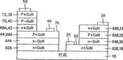
首先参考图1,根据本发明第一实施例的互补器件包括衬底10、在衬底10的第一主表面的第一部分上形成的第一场效应晶体管12和在衬底10的第一主表面的第二部分上形成的第二场效应晶体管14。在根据本发明的第一实施例的器件中,第一场效应晶体管12和第二场效应晶体管14通过开口16彼此物理隔离且电绝缘。Referring first to FIG. 1, a complementary device according to a first embodiment of the present invention includes a
根据本发明的一个方面,第一场效应晶体管12基于III-氮化物半导体。在优选实施例中,用于形成第一场效应晶体管12的III-氮化物材料是GaN。更具体地说,第一场效应晶体管12包括含N+GaN的第一导电区18、含N-GaN的第二导电区20、含P+GaN的基区22和含N+GaN的第三导电区24。第一导电区18是漏区,第二导电区20是漂移区,第三导电区24是第一场效应晶体管12的源区。第一场效应晶体管12还包括第一欧姆接触26,即欧姆连接到第一导电区18的漏极接触,第二欧姆接触28,即欧姆连接到第四导电区24的源极接触,以及栅结构30。栅结构30包括栅电极32以及插在栅电极32和基区22之间的栅绝缘34。栅电极32电连接至栅接触36。According to one aspect of the invention, the first
在本发明的优选实施例中,栅绝缘34包含SiN、Al2O3、HfO、MgO或SiO2,欧姆接触26、28可包含例如Ti、Al、Ni、Au或诸如TiAl堆叠的任何合适的金属堆叠,栅接触36可以包含诸如TiW或NiAu的任何合适的导电材料,栅电极32可包含任何合适的导体。In a preferred embodiment of the invention, the
根据本发明的第一方面,第一欧姆接触26和第二欧姆接触28各具有适用于外部电连接即焊接、引线接合等的表面26A、28A。表面26A和28A都面向相同方向,但设置在不同平面上,因此不共面。结果,器件的所有接触26、28、36在器件的一侧,但是缩短了在第一欧姆接触26和第二欧姆接触28之间的电流路径,由此改善了器件的接通电阻。According to the first aspect of the invention, the first
第二场效应晶体管14包括含P+GaN的第一导电区38、包含P-GaN的第二导电区40、包含N+GaN的基区42和包含P+GaN的第三导电区44。第一导电区38是漏区、第二导电区40是漂移区、第三导电区44是第二场效应晶体管14的源区。第二场效应晶体管还包括第一欧姆接触46,即漏极接触,第二欧姆接触48,即源极接触,以及栅结构50。栅结构50包括栅电极52以及插在栅电极52和基区42之间的栅绝缘54。第二场效应晶体管14还包括栅接触56,其电连接到栅电极52。The second
如在上述描述中已显而易见的那样,第一场效应晶体管12和第二场效应晶体管14是互补器件,因为一个器件中的每个区域的电导率与另一个器件中的相应区域的电导率相反。从而,第一场效应晶体管12包括P型基区,因此是N沟道器件,而第二场效应晶体管14包括N型基区,因此是P沟道器件。As has been evident in the foregoing description, the first
为了制造根据本发明的器件,提供管芯58,其包括衬底10和导电GaN层的堆叠60。更具体地说,堆叠60包括在衬底10的第一主表面的顶部的第一N+GaN层62、N-GaN层64、第一P+GaN层66、第二N+GaN层68、P-GaN层70和第二P+GaN层72。衬底10可包含任何已知的衬底材料,例如蓝宝石、SiC或Si,且GaN层62-72可通过任何已知方式彼此在顶部外延形成以构建堆叠60。To fabricate a device according to the invention, a
下面参考附图2A,在第一步骤中,去除P+GaN层72的一部分和P-GaN层70的一部分,暴露出第二N+GaN层68。接下来,去除第二N+GaN层68的一部分,暴露出第一P+GaN层66,留下在P-GaN层70下的第二N+GaN层68的第一部分,以及与第一部分隔开的N+GaN 68的另一部分,如图2C所示。也就是说,去除第二N+GaN层68的一部分,以在其一个部分68A和其另一部分68B之间产生开口74。Referring now to FIG. 2A , in the first step, a part of the P+
下面参考图2D,去除第一P+GaN层66的一部分和N-GaN层64的一部分,在第一P+GaN层的第一部分66A和第二部分66B之间以及N-GaN层的第一部分64A和第二部分64B之间产生开口76。开口76具有的宽度小于开口74的宽度,由此第一P+GaN层66的第一部分66A留有露出的表面78。Referring now to FIG. 2D, a part of the first P+
下面参考图2E,去除第一N+GaN层62的一部分,以在第一N+GaN层的第一部分62A和第二部分62B之间产生开口80。开口80具有的宽度小于开口76的宽度,由此N+GaN层的第二部分62B的表面82通过开口76露出。Referring now to FIG. 2E , a portion of the first N+
下面参考图2F,第一欧姆接触26形成于第一N+GaN层的第二部分62B的表面82上,第二欧姆接触28形成于第二N+GaN层的第二部分68B上,然后退火。Referring now to FIG. 2F, the first
下面参考图2G,第二场效应晶体管14的第一接触46形成于第一P+GaN的第一部分66A的表面78上,第二欧姆接触50形成于第二P+GaN层上。然后,将第一接触46和第二接触50退火。随后,形成栅结构30和栅结构50以得到如图1所示根据本发明的第一实施例的器件。为了示意在工艺完成前图2G所示的结构与最终器件之间的关系,图2G中的每个区域也标有如图1所示的最终器件中的对应区域的数字。Referring now to FIG. 2G , the
在根据本发明的方法中,在连续的步骤中蚀刻包括不同电导率的多个导电半导体层的半导体本体,以形成不同宽度的开口,以便可在不同平面上形成欧姆接触。In the method according to the invention, a semiconductor body comprising a plurality of conductive semiconductor layers of different conductivities is etched in successive steps to form openings of different widths so that ohmic contacts can be formed on different planes.
下面参考图3,根据本发明第二实施例的器件还包括含III-氮化物材料的半导体层84,形成于每个栅结构30、50和邻近半导体堆叠之间。从而,半导体层84插在栅结构30与包括第一器件12的第二导电层20、基区层22和第三导电区24的堆叠之间,另一半导体层84插在栅结构50与包括第二器件14的基区42、第二导电区40和第一导电区38的堆叠之间。半导体层84还在每个半导体堆叠中的顶部半导体层24、38上延伸。Referring now to FIG. 3 , the device according to the second embodiment of the present invention further includes a
半导体层84优选包含III-氮化物材料,该材料具有比它在其上形成的材料高的带隙。在优选实施例中,半导体层84包含AlGaN。半导体层84的加入改善了迁移率。
为了制造根据本发明第二实施例的器件,通过外延方法等在图2E所示的结构上形成AlGaN层。其后,从表面78、82和开口80的底部和侧壁去除AlGaN的部分。优选地,在这同一步骤中,开口形成于在第一场效应晶体管12的第一导电区24和第二场效应晶体管14的第三导电区38上的AlGaN层中,用于分别接收欧姆接触28和欧姆接触46。To manufacture the device according to the second embodiment of the present invention, an AlGaN layer is formed on the structure shown in FIG. 2E by an epitaxial method or the like. Thereafter, portions of AlGaN are removed from
下面参考图4,在根据本发明第三实施例的器件中,栅接触36在第二场效应晶体管12的第三导电区24上延伸。为了使栅接触36与第三导电区24绝缘,绝缘34在栅接触36下的第三导电区24上延伸。另外,减小第二场效应晶体管14的栅结构50的厚度,使得其仅比第二场效应晶体管14的基区42稍厚,但厚度不足以到达第一导电区38。而且,欧姆接触26和欧姆接触46延伸到开口80的底部并彼此短路,由此优选地填充开口80。Referring now to FIG. 4 , in a device according to a third embodiment of the invention, the
参考图5,在根据本发明第四实施例的器件中,半导体层84形成于与根据第二实施例的器件相同的区域上。半导体层84优选包含III-氮化物材料,该材料具有比它在其上形成的材料高的带隙。在本发明的优选实施例中,半导体层84包含AlGaN。在所有其它方面,根据本发明第四实施例的器件与根据第三实施例的器件相同。Referring to FIG. 5, in the device according to the fourth embodiment of the present invention, a
参考图6,在根据第五实施例的器件中,在欧姆接触26和栅结构30之间存在开口86。另外,欧姆接触28直接形成于半导体层84上,而不是直接形成于第三导电区24上并与其连接。在所有其它方面,根据本发明第五实施例的器件与根据第四实施例的器件相同。Referring to FIG. 6 , in the device according to the fifth embodiment, there is an opening 86 between the
应当注意,图1和3-6示意了根据本发明的器件的一部分的横截面图。更具体地说,所述横截面图是沿着根据本发明的器件中的典型元件的本体绘制的。在根据本发明的器件中,所述元件可具有多种几何形状,包括诸如圆形、椭圆形的无角形状,或包括正方形、矩形、六边形等的多边几何形状。It should be noted that Figures 1 and 3-6 illustrate cross-sectional views of a part of a device according to the invention. More specifically, said cross-sectional view is taken along the body of typical elements in a device according to the invention. In devices according to the invention, the elements may have a variety of geometric shapes including non-angular shapes such as circles, ellipses, or polygonal geometries including squares, rectangles, hexagons and the like.
虽然已经关于特定实施例描述了本发明,但是本领域技术人员将显而易见多种其它的变化和修改以及其它应用。因此,优选地,本发明不被在此的特定公开内容限定,而仅由随附的权利要求限定。While the invention has been described with respect to particular embodiments, it is evident that various other changes and modifications, as well as other applications, will be apparent to those skilled in the art. Preferably, therefore, the invention is not limited by the specific disclosure herein, but only by the appended claims.
Claims (20)
Translated fromChineseApplications Claiming Priority (5)
| Application Number | Priority Date | Filing Date | Title |
|---|---|---|---|
| US54462904P | 2004-02-12 | 2004-02-12 | |
| US60/544,629 | 2004-02-12 | ||
| US11/056,689US8193612B2 (en) | 2004-02-12 | 2005-02-11 | Complimentary nitride transistors vertical and common drain |
| US11/056,689 | 2005-02-11 | ||
| PCT/US2005/004610WO2005079366A2 (en) | 2004-02-12 | 2005-02-14 | Complimentary nitride transistors vertical and common drain |
Publications (2)
| Publication Number | Publication Date |
|---|---|
| CN1965412A CN1965412A (en) | 2007-05-16 |
| CN1965412Btrue CN1965412B (en) | 2010-08-25 |
Family
ID=34840647
Family Applications (1)
| Application Number | Title | Priority Date | Filing Date |
|---|---|---|---|
| CN2005800123068AExpired - Fee RelatedCN1965412B (en) | 2004-02-12 | 2005-02-14 | Complimentary nitride transistors vertical and common drain |
Country Status (6)
| Country | Link |
|---|---|
| US (1) | US8193612B2 (en) |
| JP (1) | JP2007527623A (en) |
| KR (1) | KR100797169B1 (en) |
| CN (1) | CN1965412B (en) |
| DE (1) | DE112005000335T5 (en) |
| WO (1) | WO2005079366A2 (en) |
Families Citing this family (7)
| Publication number | Priority date | Publication date | Assignee | Title |
|---|---|---|---|---|
| JP2008078604A (en)* | 2006-08-24 | 2008-04-03 | Rohm Co Ltd | MIS field effect transistor and manufacturing method thereof |
| WO2015047421A1 (en)* | 2013-09-30 | 2015-04-02 | Hrl Laboratories, Llc | Normally-off iii-nitride transistors with high threshold-voltage and low on-resistance |
| WO2013032906A1 (en)* | 2011-08-29 | 2013-03-07 | Efficient Power Conversion Corporation | Parallel connection methods for high performance transistors |
| US9269713B2 (en)* | 2013-06-04 | 2016-02-23 | Infineon Technologies Austria Ag | Semiconductor device and method for producing the same |
| US9536800B2 (en) | 2013-12-07 | 2017-01-03 | Fairchild Semiconductor Corporation | Packaged semiconductor devices and methods of manufacturing |
| TWI660465B (en)* | 2017-07-28 | 2019-05-21 | 新唐科技股份有限公司 | Semiconductor device and manufacturing method thereof |
| CN110649019A (en)* | 2019-10-11 | 2020-01-03 | 深圳第三代半导体研究院 | A kind of integrated silicon carbide transistor and its manufacturing method |
Citations (6)
| Publication number | Priority date | Publication date | Assignee | Title |
|---|---|---|---|---|
| US5502321A (en)* | 1993-11-08 | 1996-03-26 | Sharp Kabushiki Kaisha | Flash memory having inclined channel |
| US5897354A (en)* | 1996-12-17 | 1999-04-27 | Cypress Semiconductor Corporation | Method of forming a non-volatile memory device with ramped tunnel dielectric layer |
| US6147379A (en)* | 1998-04-13 | 2000-11-14 | Matsushita Electric Industrial Co., Ltd. | Semiconductor device and method for fabricating the same |
| US6184553B1 (en)* | 1998-01-16 | 2001-02-06 | Matsushita Electric Industrial Co., Ltd. | Nonvolatile semiconductor memory device and method for fabricating the same, and semiconductor integrated circuit device |
| US6362504B1 (en)* | 1995-11-22 | 2002-03-26 | Philips Electronics North America Corporation | Contoured nonvolatile memory cell |
| CN1377092A (en)* | 2001-03-27 | 2002-10-30 | 松下电器产业株式会社 | Semiconductor device |
Family Cites Families (25)
| Publication number | Priority date | Publication date | Assignee | Title |
|---|---|---|---|---|
| JPH07105497B2 (en) | 1990-01-31 | 1995-11-13 | 新技術事業団 | Semiconductor device and manufacturing method thereof |
| US5087581A (en)* | 1990-10-31 | 1992-02-11 | Texas Instruments Incorporated | Method of forming vertical FET device with low gate to source overlap capacitance |
| JP2991489B2 (en)* | 1990-11-30 | 1999-12-20 | 株式会社東芝 | Semiconductor device |
| JP2768097B2 (en)* | 1991-12-25 | 1998-06-25 | 日本電気株式会社 | Tunnel transistor |
| JP3229012B2 (en) | 1992-05-21 | 2001-11-12 | 株式会社東芝 | Method for manufacturing semiconductor device |
| US5283456A (en)* | 1992-06-17 | 1994-02-01 | International Business Machines Corporation | Vertical gate transistor with low temperature epitaxial channel |
| JP3403231B2 (en) | 1993-05-12 | 2003-05-06 | 三菱電機株式会社 | Semiconductor device and manufacturing method thereof |
| KR100193102B1 (en)* | 1994-08-25 | 1999-06-15 | 무명씨 | Semiconductor device and manufacturing method thereof |
| JP3393956B2 (en)* | 1995-06-08 | 2003-04-07 | 松下電器産業株式会社 | Vertical field effect transistor, method of manufacturing the same, and complementary vertical field effect transistor |
| JPH08116068A (en) | 1994-08-25 | 1996-05-07 | Matsushita Electric Ind Co Ltd | Semiconductor device and manufacturing method thereof |
| US5705830A (en) | 1996-09-05 | 1998-01-06 | Northrop Grumman Corporation | Static induction transistors |
| CA2242693C (en)* | 1997-09-04 | 2002-09-17 | Becton, Dickinson And Company | Additive formulation and method of use thereof |
| JP2000208760A (en)* | 1999-01-13 | 2000-07-28 | Furukawa Electric Co Ltd:The | Field effect transistor |
| DE19922855C1 (en)* | 1999-05-19 | 2001-02-01 | Draeger Medizintech Gmbh | Patient monitoring device has transportable peripheral device coupled to stationary medical station selectively combined with transportable display module and extension module |
| JP2001320052A (en)* | 2000-05-02 | 2001-11-16 | Fujitsu Ltd | Semiconductor device and semiconductor integrated circuit |
| US6396085B1 (en) | 2000-04-25 | 2002-05-28 | The Furukawa Electric Co., Ltd | GaN-type semiconductor vertical field effect transistor |
| JP4190754B2 (en) | 2001-11-27 | 2008-12-03 | 古河電気工業株式会社 | Method for manufacturing field effect transistor |
| KR100406578B1 (en) | 2001-12-29 | 2003-11-20 | 동부전자 주식회사 | Method for fabricating semiconductor device |
| KR100476691B1 (en)* | 2002-04-18 | 2005-03-18 | 삼성전자주식회사 | Method for Shallow Trench Isolation and Method of manufacturing Non-Volatile Memory Device comprising the same |
| JP4114390B2 (en)* | 2002-04-23 | 2008-07-09 | 株式会社デンソー | Semiconductor device and manufacturing method thereof |
| US6936869B2 (en)* | 2002-07-09 | 2005-08-30 | International Rectifier Corporation | Heterojunction field effect transistors using silicon-germanium and silicon-carbon alloys |
| US6822301B2 (en)* | 2002-07-31 | 2004-11-23 | Infineon Technologies Ag | Maskless middle-of-line liner deposition |
| US6825559B2 (en)* | 2003-01-02 | 2004-11-30 | Cree, Inc. | Group III nitride based flip-chip intergrated circuit and method for fabricating |
| JP4645034B2 (en)* | 2003-02-06 | 2011-03-09 | 株式会社豊田中央研究所 | Semiconductor device having group III nitride semiconductor |
| US7119380B2 (en)* | 2004-12-01 | 2006-10-10 | Semisouth Laboratories, Inc. | Lateral trench field-effect transistors in wide bandgap semiconductor materials, methods of making, and integrated circuits incorporating the transistors |
- 2005
- 2005-02-11USUS11/056,689patent/US8193612B2/ennot_activeExpired - Lifetime
- 2005-02-14KRKR1020067016787Apatent/KR100797169B1/ennot_activeExpired - Fee Related
- 2005-02-14WOPCT/US2005/004610patent/WO2005079366A2/enactiveApplication Filing
- 2005-02-14DEDE112005000335Tpatent/DE112005000335T5/ennot_activeWithdrawn
- 2005-02-14JPJP2006553315Apatent/JP2007527623A/enactivePending
- 2005-02-14CNCN2005800123068Apatent/CN1965412B/ennot_activeExpired - Fee Related
Patent Citations (6)
| Publication number | Priority date | Publication date | Assignee | Title |
|---|---|---|---|---|
| US5502321A (en)* | 1993-11-08 | 1996-03-26 | Sharp Kabushiki Kaisha | Flash memory having inclined channel |
| US6362504B1 (en)* | 1995-11-22 | 2002-03-26 | Philips Electronics North America Corporation | Contoured nonvolatile memory cell |
| US5897354A (en)* | 1996-12-17 | 1999-04-27 | Cypress Semiconductor Corporation | Method of forming a non-volatile memory device with ramped tunnel dielectric layer |
| US6184553B1 (en)* | 1998-01-16 | 2001-02-06 | Matsushita Electric Industrial Co., Ltd. | Nonvolatile semiconductor memory device and method for fabricating the same, and semiconductor integrated circuit device |
| US6147379A (en)* | 1998-04-13 | 2000-11-14 | Matsushita Electric Industrial Co., Ltd. | Semiconductor device and method for fabricating the same |
| CN1377092A (en)* | 2001-03-27 | 2002-10-30 | 松下电器产业株式会社 | Semiconductor device |
Non-Patent Citations (2)
| Title |
|---|
| JP特开2000-307101A 2000.11.02 |
| JP特开平7-131056A 1995.05.19 |
Also Published As
| Publication number | Publication date |
|---|---|
| US20050179096A1 (en) | 2005-08-18 |
| WO2005079366A3 (en) | 2007-01-11 |
| KR20060112691A (en) | 2006-11-01 |
| WO2005079366A2 (en) | 2005-09-01 |
| CN1965412A (en) | 2007-05-16 |
| US8193612B2 (en) | 2012-06-05 |
| KR100797169B1 (en) | 2008-01-23 |
| DE112005000335T5 (en) | 2007-03-22 |
| WO2005079366B1 (en) | 2007-03-08 |
| JP2007527623A (en) | 2007-09-27 |
Similar Documents
| Publication | Publication Date | Title |
|---|---|---|
| JP5766740B2 (en) | Horizontal HEMT | |
| CN102292812B (en) | Semiconductor structure, integrated circuit including semiconductor structure, and method of manufacturing semiconductor structure | |
| US9450091B2 (en) | Semiconductor device with enhanced mobility and method | |
| CN104319238B (en) | Form the method and its structure of high electron mobility semiconductor device | |
| JP6367533B2 (en) | Normally-off high electron mobility transistor | |
| EP2465141B1 (en) | Gallium nitride microwave and power switching transistors with matrix layout | |
| CN103065968B (en) | There is semiconductor device and the manufacture method thereof of perforation contact | |
| US9324645B2 (en) | Method and system for co-packaging vertical gallium nitride power devices | |
| US8937317B2 (en) | Method and system for co-packaging gallium nitride electronics | |
| CN120709226A (en) | semiconductor devices | |
| CN104659025A (en) | Method and system for interleaved boost converter with co-packaged gallium nitride power devices | |
| CN104599971A (en) | Method for manufacturing vertical semiconductor device and vertical semiconductor device | |
| CN103545251A (en) | Method for forming semiconductor device | |
| CN1965412B (en) | Complimentary nitride transistors vertical and common drain | |
| CN112670340B (en) | P-gate HEMT device | |
| JPH11266018A (en) | Semiconductor device | |
| US9466688B2 (en) | Semiconductor device with multilayer contact and method of manufacturing the same | |
| CN223080398U (en) | Gallium nitride power device structure with novel field plate | |
| CN115812253B (en) | Nitride-based semiconductor device and method of manufacturing the same | |
| CN116964750A (en) | Vertical transistor with grid connection grid | |
| CN118173594A (en) | Field Effect Transistor |
Legal Events
| Date | Code | Title | Description |
|---|---|---|---|
| C06 | Publication | ||
| PB01 | Publication | ||
| C10 | Entry into substantive examination | ||
| SE01 | Entry into force of request for substantive examination | ||
| C14 | Grant of patent or utility model | ||
| GR01 | Patent grant | ||
| CP01 | Change in the name or title of a patent holder | Address after:California, USA Patentee after:Infineon Technologies Americas Corp. Address before:California, USA Patentee before:INTERNATIONAL RECTIFIER Corp. | |
| CP01 | Change in the name or title of a patent holder | ||
| CF01 | Termination of patent right due to non-payment of annual fee | Granted publication date:20100825 | |
| CF01 | Termination of patent right due to non-payment of annual fee |