CN1964084A - Light-emitting diode packaging structure - Google Patents
Light-emitting diode packaging structureDownload PDFInfo
- Publication number
- CN1964084A CN1964084ACNA2005101152163ACN200510115216ACN1964084ACN 1964084 ACN1964084 ACN 1964084ACN A2005101152163 ACNA2005101152163 ACN A2005101152163ACN 200510115216 ACN200510115216 ACN 200510115216ACN 1964084 ACN1964084 ACN 1964084A
- Authority
- CN
- China
- Prior art keywords
- bumps
- emitting diode
- packaging structure
- structure according
- led
- Prior art date
- Legal status (The legal status is an assumption and is not a legal conclusion. Google has not performed a legal analysis and makes no representation as to the accuracy of the status listed.)
- Pending
Links
- 238000004806packaging method and processMethods0.000titleclaimsabstractdescription37
- 230000009975flexible effectEffects0.000claimsabstractdescription50
- 239000000758substrateSubstances0.000claimsabstractdescription18
- 230000017525heat dissipationEffects0.000claimsdescription18
- 239000000463materialSubstances0.000claimsdescription17
- 239000000853adhesiveSubstances0.000claimsdescription16
- 230000001070adhesive effectEffects0.000claimsdescription16
- 239000004020conductorSubstances0.000claimsdescription14
- 229910000679solderInorganic materials0.000claimsdescription11
- PXHVJJICTQNCMI-UHFFFAOYSA-NNickelChemical compound[Ni]PXHVJJICTQNCMI-UHFFFAOYSA-N0.000claimsdescription6
- RYGMFSIKBFXOCR-UHFFFAOYSA-NCopperChemical compound[Cu]RYGMFSIKBFXOCR-UHFFFAOYSA-N0.000claimsdescription5
- 229910052802copperInorganic materials0.000claimsdescription5
- 239000010949copperSubstances0.000claimsdescription5
- 229910052782aluminiumInorganic materials0.000claimsdescription3
- XAGFODPZIPBFFR-UHFFFAOYSA-NaluminiumChemical compound[Al]XAGFODPZIPBFFR-UHFFFAOYSA-N0.000claimsdescription3
- PCHJSUWPFVWCPO-UHFFFAOYSA-NgoldChemical compound[Au]PCHJSUWPFVWCPO-UHFFFAOYSA-N0.000claimsdescription3
- 239000010931goldSubstances0.000claimsdescription3
- 229910052737goldInorganic materials0.000claimsdescription3
- 229910052759nickelInorganic materials0.000claimsdescription3
- 239000007769metal materialSubstances0.000claimsdescription2
- 238000005452bendingMethods0.000description8
- 238000010586diagramMethods0.000description4
- 238000000034methodMethods0.000description4
- 239000004065semiconductorSubstances0.000description4
- 239000004642PolyimideSubstances0.000description3
- 238000005516engineering processMethods0.000description3
- 229920001721polyimidePolymers0.000description3
- 150000001875compoundsChemical class0.000description2
- 238000000605extractionMethods0.000description2
- 239000012811non-conductive materialSubstances0.000description2
- JMASRVWKEDWRBT-UHFFFAOYSA-NGallium nitrideChemical compound[Ga]#NJMASRVWKEDWRBT-UHFFFAOYSA-N0.000description1
- 229910052581Si3N4Inorganic materials0.000description1
- 238000001816coolingMethods0.000description1
- PMHQVHHXPFUNSP-UHFFFAOYSA-Mcopper(1+);methylsulfanylmethane;bromideChemical groupBr[Cu].CSCPMHQVHHXPFUNSP-UHFFFAOYSA-M0.000description1
- 239000013078crystalSubstances0.000description1
- 230000005496eutecticsEffects0.000description1
- 230000010354integrationEffects0.000description1
- 238000012986modificationMethods0.000description1
- 230000004048modificationEffects0.000description1
- 238000012536packaging technologyMethods0.000description1
- 239000011347resinSubstances0.000description1
- 229920005989resinPolymers0.000description1
- HQVNEWCFYHHQES-UHFFFAOYSA-Nsilicon nitrideChemical compoundN12[Si]34N5[Si]62N3[Si]51N64HQVNEWCFYHHQES-UHFFFAOYSA-N0.000description1
Images
Classifications
- H—ELECTRICITY
- H01—ELECTRIC ELEMENTS
- H01L—SEMICONDUCTOR DEVICES NOT COVERED BY CLASS H10
- H01L2224/00—Indexing scheme for arrangements for connecting or disconnecting semiconductor or solid-state bodies and methods related thereto as covered by H01L24/00
- H01L2224/01—Means for bonding being attached to, or being formed on, the surface to be connected, e.g. chip-to-package, die-attach, "first-level" interconnects; Manufacturing methods related thereto
- H01L2224/10—Bump connectors; Manufacturing methods related thereto
- H01L2224/15—Structure, shape, material or disposition of the bump connectors after the connecting process
- H01L2224/16—Structure, shape, material or disposition of the bump connectors after the connecting process of an individual bump connector
- H01L2224/161—Disposition
- H01L2224/16151—Disposition the bump connector connecting between a semiconductor or solid-state body and an item not being a semiconductor or solid-state body, e.g. chip-to-substrate, chip-to-passive
- H01L2224/16221—Disposition the bump connector connecting between a semiconductor or solid-state body and an item not being a semiconductor or solid-state body, e.g. chip-to-substrate, chip-to-passive the body and the item being stacked
- H01L2224/16225—Disposition the bump connector connecting between a semiconductor or solid-state body and an item not being a semiconductor or solid-state body, e.g. chip-to-substrate, chip-to-passive the body and the item being stacked the item being non-metallic, e.g. insulating substrate with or without metallisation
Landscapes
- Led Device Packages (AREA)
Abstract
Description
Translated fromChinese技术领域technical field
本发明是有关于一种半导体封装元件,且特别是有关于一种发光二极管的封装结构。The present invention relates to a semiconductor packaging component, and in particular to a packaging structure of a light emitting diode.
背景技术Background technique
由III-N族元素化合物半导体材料所构成的发光二极管(LightEmitting Diode,简称LED)是一种宽能隙(bandgap)的发光元件,其可发出的光线从红外光一直到紫外光,而涵盖所有可见光的波段。近年来,随着高亮度氮化镓(GaN)蓝/绿光发光二极管的快速发展,全彩发光二极管显示器、白光发光二极管及发光二极管交通号志等得以实用化,而其他各种发光二极管的应用也更加普及。Light Emitting Diode (LED for short) composed of III-N group element compound semiconductor materials is a light-emitting element with a wide bandgap (bandgap), which can emit light from infrared light to ultraviolet light, covering all visible light band. In recent years, with the rapid development of high-brightness gallium nitride (GaN) blue/green light-emitting diodes, full-color light-emitting diode displays, white light-emitting diodes, and light-emitting diode traffic signals have been put into practical use, while other kinds of light-emitting diodes Apps are also more ubiquitous.
发光二极管元件的基本结构包含P型及N型的III-V族元素化合物磊晶层,以及其间的主动层(active layer),也就是发光层。发光二极管元件的发光效率高低是取决于主动层的量子效率(internal quantumefficiency),以及该元件的光取出效率(light extraction efficiency)。增加量子效率的方法主要是改善主动层的长晶品质及其磊晶层(epitaxiallayer)结构设计,而增加光取出效率的关键则在于减少主动层所发出的光在发光二极管内部反射所造成的能量损失。The basic structure of a light-emitting diode device includes P-type and N-type III-V group element compound epitaxial layers, and an active layer therebetween, that is, a light-emitting layer. The luminous efficiency of the LED device depends on the internal quantum efficiency of the active layer and the light extraction efficiency of the device. The method to increase the quantum efficiency is mainly to improve the crystal growth quality of the active layer and the structural design of the epitaxial layer (epitaxial layer), and the key to increasing the light extraction efficiency is to reduce the energy caused by the light emitted by the active layer reflected inside the light-emitting diode. loss.
习知的发光二极管封装结构包括一承载器(carrier)以及一发光二极管晶片(LED Chip),其中承载器包括一基板与一线路层,而基板的材质为氮化铝或氮化硅,亦即承载器为硬式承载器。在习知技术中,发光二极管晶片是藉由凸块与承载器上的线路层电性连接。A conventional light emitting diode packaging structure includes a carrier and a light emitting diode chip (LED Chip), wherein the carrier includes a substrate and a circuit layer, and the material of the substrate is aluminum nitride or silicon nitride, that is The carrier is a rigid carrier. In the conventional technology, the LED chip is electrically connected to the circuit layer on the carrier through bumps.
值得注意的是,当多个发光二极管晶片封装于一承载器时,由于发光二极管封装结构的承载器是为硬式承载器,即承载器不具有可挠性,故习知的发光二极管封装结构的使用空间将有所限制。因此,在电子产品均要求轻薄短小的趋势下,如何使发光二极管封装结构具有可挠性质以增加其空间使用上的弹性是一重要课题。It is worth noting that when a plurality of LED chips are packaged on a carrier, since the carrier of the LED packaging structure is a rigid carrier, that is, the carrier is not flexible, the conventional LED packaging structure Space usage will be limited. Therefore, under the trend that electronic products are required to be light, thin, and small, how to make the light emitting diode packaging structure flexible to increase the flexibility of its space usage is an important issue.
发明内容Contents of the invention
有鉴于此,本发明的目的就是在提供一种发光二极管封装结构,其具有可挠性的软性承载器。In view of this, the purpose of the present invention is to provide a light emitting diode packaging structure, which has a flexible soft carrier.
为达本发明的上述目的,本发明提出一种发光二极管封装结构,其包括一发光二极管晶片与一软性承载器,其中发光二极管晶片具有多个电极。软性承载器则具有一软性基板与一线路层,其中软性基板具有一承载表面与对应的一背面,而线路层是配置于承载表面上。此外,发光二极管晶片的电极是与软性承载器的线路层电性连接。In order to achieve the above object of the present invention, the present invention proposes a LED packaging structure, which includes a LED chip and a flexible carrier, wherein the LED chip has a plurality of electrodes. The flexible carrier has a flexible substrate and a circuit layer, wherein the flexible substrate has a carrying surface and a corresponding back surface, and the circuit layer is configured on the carrying surface. In addition, the electrodes of the LED chip are electrically connected with the circuit layer of the flexible carrier.
在本发明的一实施例中,软性承载器更包括一配置于线路层上的防焊层,且防焊层暴露出与电极电性连接的线路层。In an embodiment of the present invention, the flexible carrier further includes a solder resist layer disposed on the circuit layer, and the solder resist layer exposes the circuit layer electrically connected to the electrodes.
在本发明的一实施例中,发光二极管封装结构更包括多个凸块,每一个电极上配置有一凸块,其中线路层是经由凸块与电极电性连接。此外,凸块例如是金凸块、铜凸块、镍凸块或是铝凸块。In an embodiment of the present invention, the LED packaging structure further includes a plurality of bumps, and a bump is disposed on each electrode, wherein the circuit layer is electrically connected to the electrodes through the bumps. In addition, the bumps are, for example, gold bumps, copper bumps, nickel bumps or aluminum bumps.
在本发明的一实施例中,凸块的材料可以为导电型B阶胶材。In an embodiment of the present invention, the material of the bump may be a conductive B-stage adhesive.
在本发明的一实施例中,发光二极管封装结构更包括一导电材料,其中导电材料配置于线路层与每一个凸块之间,且线路层经由导电材料与每一个凸块电性连接。此外,导电材料例如是焊料、导电型B阶胶材、异方性导电膜或异方性导电胶。In an embodiment of the present invention, the LED packaging structure further includes a conductive material, wherein the conductive material is disposed between the wiring layer and each bump, and the wiring layer is electrically connected to each bump through the conductive material. In addition, the conductive material is, for example, solder, conductive B-stage adhesive material, anisotropic conductive film or anisotropic conductive adhesive.
在本发明的一实施例中,软性承载器例如是软性电路板,而软性基板的材料例如是聚亚酰胺。In an embodiment of the present invention, the flexible carrier is, for example, a flexible circuit board, and the material of the flexible substrate is, for example, polyimide.
在本发明的一实施例中,发光二极管封装结构更包括一散热元件,散热元件是贴附于软性基板的背面。此外,软性基板具有多个填充金属材料的散热孔,且这些散热孔配置在散热元件所覆盖的区域。In an embodiment of the present invention, the LED package structure further includes a heat dissipation element, and the heat dissipation element is attached to the back of the flexible substrate. In addition, the flexible substrate has a plurality of heat dissipation holes filled with metal material, and these heat dissipation holes are arranged in the area covered by the heat dissipation element.
在本发明的一实施例中,线路层的材料例如是铜。In an embodiment of the invention, the material of the wiring layer is copper, for example.
基于上述,在本发明中,发光二极管封装结构是具有可挠性的软性承载器,使得发光二极管封装结构具有可挠性质,进而增加发光二极管封装结构在不同空间内的使用弹性。Based on the above, in the present invention, the LED packaging structure is a flexible soft carrier, so that the LED packaging structure has a flexible property, thereby increasing the flexibility of using the LED packaging structure in different spaces.
为让本发明的上述和其他目的、特征和优点能更明显易懂,下文特举多个实施例,并配合所附图式,作详细说明如下。In order to make the above and other objects, features and advantages of the present invention more comprehensible, a number of embodiments will be described in detail below together with the accompanying drawings.
附图说明Description of drawings
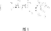
图1是本发明第一实施例的发光二极管封装结构的示意图。FIG. 1 is a schematic diagram of a light emitting diode package structure according to a first embodiment of the present invention.
图2是本发明第二实施例的发光二极管封装结构的示意图。FIG. 2 is a schematic diagram of a light emitting diode package structure according to a second embodiment of the present invention.
100、200:发光二极管封装结构 110:发光二极管晶片100, 200: Light-emitting diode packaging structure 110: Light-emitting diode chip
112:电极 120:软性承载器112: Electrode 120: Soft carrier
122:软性基板 122a:承载表面122:
122b:背面 124:线路层122b: Back side 124: Circuit layer
126:防焊层 130:凸块126: Solder mask 130: Bump
140:导电材料 150:散热元件140: Conductive material 150: Heat dissipation element
202:弯折区202: bending area
具体实施方式Detailed ways
图1是本发明第一实施例的发光二极管封装结构的示意图。由图1可知,本实施例的发光二极管封装结构100包括发光二极管晶片110与软性承载器120,其中发光二极管晶片110具有多个电极112。此外,软性承载器120具有一软性基板122与一线路层124,软性基板122是具有一承载表面122a与对应的一背面122b,而线路层124即配置于承载表面122a上。FIG. 1 is a schematic diagram of a light emitting diode package structure according to a first embodiment of the present invention. As can be seen from FIG. 1 , the
另一方面,发光二极管封装结构200更可包括多个凸块130,其中凸块130是配置于电极112上,而线路层124即是经由凸块130与电极112电性连接。在此,凸块130例如是金凸块、铜凸块、镍凸块或是铝凸块,而线路层124的材料例如是铜。在本实施例中,软性承载器120亦可包括一防焊层126,其中防焊层126是配置于线路层124上且暴露出与电极112电性连接的线路层124。On the other hand, the LED packaging structure 200 may further include a plurality of
在此,将针对软性承载器120做详细说明。在本实施例中,软性承载器120例如是软性电路板(Flexible Printed Circuit board,简称FPC),而软性承载器120的软性基板122的材料例如是聚亚酰胺(Polyimide,简称PI)。因此,藉由覆晶封装技术将发光二极管晶片110配置于软性承载器120上的后,即可使发光二极管封装结构100具有良好的可挠性质,进而增加发光二极管封装结构100在空间上的使用弹性。Here, the
承上所述,为使凸块130与线路层124能有良好的电性连接关系,发光二极管封装结构200例如更包括一导电材料140,其中导电材料140是配置于线路层124与凸块130之间。因此,线路层124即可经由导电材料140顺利地与凸块130电性连接,而使导电材料140与凸块130电性连接的方式可以是热压接合技术。举例来说,导电材料140可以是焊料、导电型B阶胶材(Conductive B-stage adhesive)、异方性导电膜(AnisotropicConductive Film,简称ACF)或是异方性导电胶(Anisotropic ConductivePaste,简称ACP)。Based on the above, in order to make the
当然,凸块可直接为导电型B阶胶材。如此,线路层与电极即具有电性连接的关系。除了上述的电性连接方式外,本发明在此亦提供多种使线路层与电极电性连接且能保护凸块不受损害的方式。举例来说,可以用热压(eutectic)或者是超音波接合方式让凸块直接与电极电性连接,并应用毛细现象来使非导电性材料附着于凸块表面及部分发光二极管晶片表面,凸块与发光二极管晶片即不易受外界环境影响而损坏,其中非导电性材料可以是树酯(resin)。Of course, the bump can be directly a conductive B-stage adhesive. In this way, the circuit layer and the electrodes are electrically connected. In addition to the above-mentioned electrical connection methods, the present invention also provides various methods for electrically connecting the circuit layer and the electrodes and protecting the bumps from damage. For example, the bump can be directly electrically connected to the electrode by means of eutectic or ultrasonic bonding, and the capillary phenomenon can be used to make the non-conductive material adhere to the surface of the bump and part of the surface of the LED chip. The block and the LED chip are not easily damaged by the external environment, and the non-conductive material can be resin.
另一方面,本发明亦可应用非导电性胶材来取代上述的导电胶材,并使凸块挤压非导电性胶材以与电极连接。更详细地说,凸块是与电极具有电性连接的关系,其中本发明是以热压方式或是超音波方式使凸块与电极达成电性连接。值得注意的是,非导电性胶材会受到凸块挤压而附着于凸块的部分表面上。如此,非导电性胶材亦可达到保护凸块不受损坏的功效。在此非导电性胶材例如是B阶胶材。On the other hand, the present invention can also use a non-conductive adhesive material to replace the above-mentioned conductive adhesive material, and make the bump press the non-conductive adhesive material to connect with the electrode. More specifically, the bump is electrically connected to the electrode, and the present invention achieves electrical connection between the bump and the electrode by means of heat pressing or ultrasonic wave. It should be noted that the non-conductive adhesive material will be pressed by the bump and adhere to part of the surface of the bump. In this way, the non-conductive adhesive material can also achieve the function of protecting the bumps from being damaged. Here, the non-conductive adhesive material is, for example, a B-stage adhesive material.
值得注意的是,随着半导体元件的积集度、操作功率提高,半导体元件单位面积所散发的热量也会随的提高,为解决上述的散热问题,本实施例的发光二极管封装结构100可应用一散热元件150来辅助发光二极管晶片110进行散热。散热元件150是贴附于软性基板122的背面122b,其中可以藉由一导热性粘着材料连接于背面122b与散热元件150之间,发光二极管晶片110所产生的热量即可传递至散热元件150,以降低发光二极管晶片110的内部温度。此外,为了达到较佳的散热效率,软性基板120上可以具有多个散热孔(未绘示),散热孔例如是配置在散热元件150所覆盖的区域,其中散热孔可填充金属材料以增加发光二极管晶片110的散热效率。It is worth noting that as the integration degree and operating power of semiconductor elements increase, the heat dissipated per unit area of semiconductor elements will also increase accordingly. In order to solve the above heat dissipation problem, the
图2是本发明第二实施例的发光二极管封装结构的示意图。由图2可知,本实施例的发光二极管封装结构200与第二实施例的发光二极管封装结构100类似,惟二者的主要差异在于:本实施例的发光二极管封装结构200包括二个发光二极管晶片110,且具有一弯折区202。换言之,本实施例的发光二极管封装结构200同样具有良好的可挠性质。在本实施例中,发光二极管封装结构200藉由弯折区202使得二个发光二极管晶片110在软性承载器120上的配设位置有所变化。举例来说,二个发光二极管晶片110可分别配设于弯折区202的一侧,其中弯折区202是藉由对软性承载器120进行弯折的作动以形成的。值得注意的是,当二个发光二极管晶片110分别配设于弯折区202的一侧时,二个发光二极管晶片110即分别具有不同的出光方向。FIG. 2 is a schematic diagram of a light emitting diode package structure according to a second embodiment of the present invention. It can be seen from FIG. 2 that the LED packaging structure 200 of this embodiment is similar to the
承上所述,当发光二极管封装结构200配置于电子产品(未绘示)时,发光二极管封装结构200可调整至适当形状以配合电子产品内部的空间设计,并可藉由二个发光二极管晶片110发出不同方向的光线。如此一来,发光二极管封装结构200应用于电子产品的实用性将可大幅增加。Based on the above, when the LED packaging structure 200 is configured in an electronic product (not shown), the LED packaging structure 200 can be adjusted to an appropriate shape to match the interior space design of the electronic product, and can be provided by two
当然,本发明在此并不限定发光二极管晶片在软性承载器上的配设位置,以及散热片在软性承载器上的配设位置与数量。此外,虽然上述实施例以具有二个发光二极管晶片与一弯折区的发光二极管封装结构为例,但本发明并不限定发光二极管晶片在发光二极管封装结构中的配设数量与软性承载器受弯折的次数。相较于习知技术,本发明的发光二极管封装结构是具有良好的可挠性质,使得发光二极管晶片藉由调整软性承载器即可改变其出光方向。换言之,本发明的发光二极管封装结构的应用范围将较为广泛。Of course, the present invention does not limit the disposition position of the LED chip on the flexible carrier, and the disposition position and quantity of the cooling fins on the flexible carrier. In addition, although the above-mentioned embodiments take the LED packaging structure with two LED chips and a bending area as an example, the present invention does not limit the number of LED chips in the LED packaging structure and the flexible carrier number of bends. Compared with the conventional technology, the LED package structure of the present invention has good flexibility, so that the light emitting direction of the LED chip can be changed by adjusting the flexible carrier. In other words, the application range of the light emitting diode package structure of the present invention will be relatively wide.
虽然本发明已以多个实施例揭露如上,然其并非用以限定本发明,任何熟习此技艺者,在不脱离本发明的精神和范围内,当可作些许的更动与润饰,因此本发明的保护范围当视前述的技术方案所界定为准。Although the present invention has been disclosed above with multiple embodiments, it is not intended to limit the present invention. Anyone skilled in the art can make some changes and modifications without departing from the spirit and scope of the present invention. Therefore, this The scope of protection of the invention should be defined by the aforementioned technical solutions.
Claims (10)
Translated fromChinesePriority Applications (1)
| Application Number | Priority Date | Filing Date | Title |
|---|---|---|---|
| CNA2005101152163ACN1964084A (en) | 2005-11-11 | 2005-11-11 | Light-emitting diode packaging structure |
Applications Claiming Priority (1)
| Application Number | Priority Date | Filing Date | Title |
|---|---|---|---|
| CNA2005101152163ACN1964084A (en) | 2005-11-11 | 2005-11-11 | Light-emitting diode packaging structure |
Publications (1)
| Publication Number | Publication Date |
|---|---|
| CN1964084Atrue CN1964084A (en) | 2007-05-16 |
Family
ID=38083049
Family Applications (1)
| Application Number | Title | Priority Date | Filing Date |
|---|---|---|---|
| CNA2005101152163APendingCN1964084A (en) | 2005-11-11 | 2005-11-11 | Light-emitting diode packaging structure |
Country Status (1)
| Country | Link |
|---|---|
| CN (1) | CN1964084A (en) |
Cited By (4)
| Publication number | Priority date | Publication date | Assignee | Title |
|---|---|---|---|---|
| CN101329042B (en)* | 2007-06-18 | 2010-12-08 | 南茂科技股份有限公司 | Light source assembly |
| CN103225755A (en)* | 2012-11-23 | 2013-07-31 | 苏州博聚材料科技有限公司 | Led lamp tube |
| CN103606545A (en)* | 2013-08-27 | 2014-02-26 | 北京半导体照明科技促进中心 | LED flexible board light source module and manufacturing method thereof |
| CN109950380A (en)* | 2017-12-21 | 2019-06-28 | 财团法人工业技术研究院 | Light Emitting Diode Package |
- 2005
- 2005-11-11CNCNA2005101152163Apatent/CN1964084A/enactivePending
Cited By (6)
| Publication number | Priority date | Publication date | Assignee | Title |
|---|---|---|---|---|
| CN101329042B (en)* | 2007-06-18 | 2010-12-08 | 南茂科技股份有限公司 | Light source assembly |
| CN103225755A (en)* | 2012-11-23 | 2013-07-31 | 苏州博聚材料科技有限公司 | Led lamp tube |
| CN103606545A (en)* | 2013-08-27 | 2014-02-26 | 北京半导体照明科技促进中心 | LED flexible board light source module and manufacturing method thereof |
| CN103606545B (en)* | 2013-08-27 | 2017-02-22 | 北京半导体照明科技促进中心 | LED flexible board light source module and manufacturing method thereof |
| CN109950380A (en)* | 2017-12-21 | 2019-06-28 | 财团法人工业技术研究院 | Light Emitting Diode Package |
| CN109950380B (en)* | 2017-12-21 | 2021-06-01 | 财团法人工业技术研究院 | Light Emitting Diode Package |
Similar Documents
| Publication | Publication Date | Title |
|---|---|---|
| US20070096272A1 (en) | Light emitting diode package | |
| JP4121536B2 (en) | Semiconductor light emitting element, method for manufacturing the same, method for mounting the same, and light emitting device | |
| TWI535077B (en) | Light emitting unit and light emitting module thereof | |
| US7808013B2 (en) | Integrated heat spreaders for light emitting devices (LEDs) and related assemblies | |
| TWI430483B (en) | Light emitting device package component and method of manufacturing same | |
| US7569420B2 (en) | Flip-chip packaging method for light emitting diode with eutectic layer not overlapping insulating layer | |
| CN102983256B (en) | LED Packaging | |
| EP1594171A2 (en) | Semiconductor light emitting device with flexible substrate | |
| US20100032705A1 (en) | Light emitting diode package and method of manufacturing the same | |
| TWI645580B (en) | Light-emitting diode flip chip and display | |
| CN102315364A (en) | LED module, LED package, and wiring substrate and method of making same | |
| CN103066180A (en) | Light emitting device (LED), manufacturing method thereof, and LED module using same | |
| US7459783B2 (en) | Light emitting chip package and light source module | |
| KR20200042215A (en) | Light emitting diode, manufacturing method of light emitting diode | |
| TWI395346B (en) | Light emitting device package structure and fabricating method thereof | |
| CN101114623B (en) | Packaging module and electronic device | |
| CN101207169A (en) | Light emitting chip package and light source assembly | |
| US10784423B2 (en) | Light emitting device | |
| CN101546737B (en) | Package structure of compound semiconductor component and manufacturing method thereof | |
| KR101166066B1 (en) | Light Emitting Diode Package | |
| CN1964084A (en) | Light-emitting diode packaging structure | |
| JP6210720B2 (en) | LED package | |
| CN101212007A (en) | Electroluminescence module | |
| CN101110408A (en) | Light emitting diode module | |
| CN105261692A (en) | Light emitting module |
Legal Events
| Date | Code | Title | Description |
|---|---|---|---|
| C06 | Publication | ||
| PB01 | Publication | ||
| C10 | Entry into substantive examination | ||
| SE01 | Entry into force of request for substantive examination | ||
| C12 | Rejection of a patent application after its publication | ||
| RJ01 | Rejection of invention patent application after publication |