CN1957247A - Optical system for generating illumination strips - Google Patents
Optical system for generating illumination stripsDownload PDFInfo
- Publication number
- CN1957247A CN1957247ACNA2005800166468ACN200580016646ACN1957247ACN 1957247 ACN1957247 ACN 1957247ACN A2005800166468 ACNA2005800166468 ACN A2005800166468ACN 200580016646 ACN200580016646 ACN 200580016646ACN 1957247 ACN1957247 ACN 1957247A
- Authority
- CN
- China
- Prior art keywords
- described optical
- light source
- light
- optical systems
- irradiation unit
- Prior art date
- Legal status (The legal status is an assumption and is not a legal conclusion. Google has not performed a legal analysis and makes no representation as to the accuracy of the status listed.)
- Granted
Links
- 230000003287optical effectEffects0.000titleclaimsabstractdescription148
- 238000005286illuminationMethods0.000titleclaimsdescription71
- 239000000463materialSubstances0.000claimsabstractdescription143
- 238000007639printingMethods0.000claimsdescription32
- 239000000758substrateSubstances0.000claimsdescription23
- 230000005855radiationEffects0.000claimsdescription21
- 239000007787solidSubstances0.000claimsdescription21
- 238000000034methodMethods0.000claimsdescription13
- 238000012545processingMethods0.000claimsdescription13
- 238000001816coolingMethods0.000claimsdescription6
- 238000007645offset printingMethods0.000claimsdescription4
- 230000008569processEffects0.000claimsdescription4
- 229920003023plasticPolymers0.000claimsdescription3
- 230000003044adaptive effectEffects0.000claims1
- 238000005452bendingMethods0.000claims1
- 239000004744fabricSubstances0.000claims1
- 239000004033plasticSubstances0.000claims1
- 238000009792diffusion processMethods0.000abstract2
- 239000002826coolantSubstances0.000description12
- 230000008901benefitEffects0.000description9
- 230000000875corresponding effectEffects0.000description9
- 238000007689inspectionMethods0.000description8
- 238000003384imaging methodMethods0.000description5
- 230000001360synchronised effectEffects0.000description4
- 230000008859changeEffects0.000description3
- 238000005259measurementMethods0.000description3
- 230000001960triggered effectEffects0.000description3
- 230000006978adaptationEffects0.000description2
- 239000011248coating agentSubstances0.000description2
- 238000000576coating methodMethods0.000description2
- 238000011109contaminationMethods0.000description2
- 230000001419dependent effectEffects0.000description2
- 238000009826distributionMethods0.000description2
- 230000000694effectsEffects0.000description2
- 238000011156evaluationMethods0.000description2
- 230000001678irradiating effectEffects0.000description2
- 239000007788liquidSubstances0.000description2
- 238000012544monitoring processMethods0.000description2
- 239000003973paintSubstances0.000description2
- 230000001105regulatory effectEffects0.000description2
- 230000002123temporal effectEffects0.000description2
- 230000009471actionEffects0.000description1
- 230000004913activationEffects0.000description1
- 230000002411adverseEffects0.000description1
- 230000032683agingEffects0.000description1
- 229910052782aluminiumInorganic materials0.000description1
- XAGFODPZIPBFFR-UHFFFAOYSA-NaluminiumChemical compound[Al]XAGFODPZIPBFFR-UHFFFAOYSA-N0.000description1
- 230000004888barrier functionEffects0.000description1
- 230000009286beneficial effectEffects0.000description1
- 230000005540biological transmissionEffects0.000description1
- 230000015572biosynthetic processEffects0.000description1
- 238000009529body temperature measurementMethods0.000description1
- 235000008429breadNutrition0.000description1
- 239000003086colorantSubstances0.000description1
- 230000008878couplingEffects0.000description1
- 238000010168coupling processMethods0.000description1
- 238000005859coupling reactionMethods0.000description1
- 238000013461designMethods0.000description1
- 238000001514detection methodMethods0.000description1
- 238000010586diagramMethods0.000description1
- 239000000428dustSubstances0.000description1
- 238000005516engineering processMethods0.000description1
- 230000005284excitationEffects0.000description1
- 238000007646gravure printingMethods0.000description1
- 229910052736halogenInorganic materials0.000description1
- 150000002367halogensChemical class0.000description1
- 238000000265homogenisationMethods0.000description1
- 238000001746injection mouldingMethods0.000description1
- 238000009434installationMethods0.000description1
- 239000011159matrix materialSubstances0.000description1
- 229910052751metalInorganic materials0.000description1
- 239000002184metalSubstances0.000description1
- 238000002156mixingMethods0.000description1
- 235000012149noodlesNutrition0.000description1
- 239000002245particleSubstances0.000description1
- 238000007650screen-printingMethods0.000description1
- 239000004065semiconductorSubstances0.000description1
- 238000000926separation methodMethods0.000description1
- 239000000243solutionSubstances0.000description1
- 238000009827uniform distributionMethods0.000description1
- XLYOFNOQVPJJNP-UHFFFAOYSA-NwaterSubstancesOXLYOFNOQVPJJNP-UHFFFAOYSA-N0.000description1
Images


Classifications
- H—ELECTRICITY
- H04—ELECTRIC COMMUNICATION TECHNIQUE
- H04N—PICTORIAL COMMUNICATION, e.g. TELEVISION
- H04N1/00—Scanning, transmission or reproduction of documents or the like, e.g. facsimile transmission; Details thereof
- H04N1/024—Details of scanning heads ; Means for illuminating the original
- H04N1/028—Details of scanning heads ; Means for illuminating the original for picture information pick-up
- H04N1/02815—Means for illuminating the original, not specific to a particular type of pick-up head
- G—PHYSICS
- G07—CHECKING-DEVICES
- G07D—HANDLING OF COINS OR VALUABLE PAPERS, e.g. TESTING, SORTING BY DENOMINATIONS, COUNTING, DISPENSING, CHANGING OR DEPOSITING
- G07D7/00—Testing specially adapted to determine the identity or genuineness of valuable papers or for segregating those which are unacceptable, e.g. banknotes that are alien to a currency
- G07D7/06—Testing specially adapted to determine the identity or genuineness of valuable papers or for segregating those which are unacceptable, e.g. banknotes that are alien to a currency using wave or particle radiation
- G07D7/12—Visible light, infrared or ultraviolet radiation
- G07D7/121—Apparatus characterised by sensor details
- H—ELECTRICITY
- H04—ELECTRIC COMMUNICATION TECHNIQUE
- H04N—PICTORIAL COMMUNICATION, e.g. TELEVISION
- H04N1/00—Scanning, transmission or reproduction of documents or the like, e.g. facsimile transmission; Details thereof
- H04N1/00976—Arrangements for regulating environment, e.g. removing static electricity
- H04N1/00978—Temperature control
- H04N1/00981—Temperature control by forced convection, e.g. using fans
- H—ELECTRICITY
- H04—ELECTRIC COMMUNICATION TECHNIQUE
- H04N—PICTORIAL COMMUNICATION, e.g. TELEVISION
- H04N1/00—Scanning, transmission or reproduction of documents or the like, e.g. facsimile transmission; Details thereof
- H04N1/024—Details of scanning heads ; Means for illuminating the original
- H04N1/028—Details of scanning heads ; Means for illuminating the original for picture information pick-up
- H04N1/02815—Means for illuminating the original, not specific to a particular type of pick-up head
- H04N1/02845—Means for illuminating the original, not specific to a particular type of pick-up head using an elongated light source, e.g. tubular lamp, LED array
- H04N1/02865—Means for illuminating the original, not specific to a particular type of pick-up head using an elongated light source, e.g. tubular lamp, LED array using an array of light sources or a combination of such arrays, e.g. an LED bar
- H—ELECTRICITY
- H04—ELECTRIC COMMUNICATION TECHNIQUE
- H04N—PICTORIAL COMMUNICATION, e.g. TELEVISION
- H04N1/00—Scanning, transmission or reproduction of documents or the like, e.g. facsimile transmission; Details thereof
- H04N1/024—Details of scanning heads ; Means for illuminating the original
- H04N1/028—Details of scanning heads ; Means for illuminating the original for picture information pick-up
- H04N1/02815—Means for illuminating the original, not specific to a particular type of pick-up head
- H04N1/02885—Means for compensating spatially uneven illumination, e.g. an aperture arrangement
- H—ELECTRICITY
- H04—ELECTRIC COMMUNICATION TECHNIQUE
- H04N—PICTORIAL COMMUNICATION, e.g. TELEVISION
- H04N1/00—Scanning, transmission or reproduction of documents or the like, e.g. facsimile transmission; Details thereof
- H04N1/024—Details of scanning heads ; Means for illuminating the original
- H04N1/028—Details of scanning heads ; Means for illuminating the original for picture information pick-up
- H04N1/02815—Means for illuminating the original, not specific to a particular type of pick-up head
- H04N1/02895—Additional elements in the illumination means or cooperating with the illumination means, e.g. filters
Landscapes
- Engineering & Computer Science (AREA)
- Multimedia (AREA)
- Signal Processing (AREA)
- General Health & Medical Sciences (AREA)
- Toxicology (AREA)
- Health & Medical Sciences (AREA)
- Physics & Mathematics (AREA)
- General Physics & Mathematics (AREA)
- Environmental & Geological Engineering (AREA)
- Investigating Materials By The Use Of Optical Means Adapted For Particular Applications (AREA)
- Non-Portable Lighting Devices Or Systems Thereof (AREA)
- Light Sources And Details Of Projection-Printing Devices (AREA)
- Lenses (AREA)
Abstract
Description
Translated fromChinese本发明涉及一种根据权利要求1、8或98的前序部分所述的用于生成照射条带的光学系统。The invention relates to an optical system for generating an illumination strip according to the preamble of
所述的光学系统主要用于对机器加工的材料,例如对有价证券印刷时加工的承印材料进行摄像,进行工业图像处理,其中光学系统应用于印刷机,优选应用于轮转印刷机,特别是应用于采用胶印印刷方法或采用凹版印刷方法或采用丝网印刷方法或采用热压方法的印刷机。除了可以设置在印刷机上,光学系统也可以设置在对印刷产品继续加工的机器中,或设置在印刷机中的同时,还可以设置在对印刷产品继续加工的机器上。可以采用或不采用对材料预先确定的特征,针对实现移动的材料的至少截取的图像,优选完全的图像显示进行摄像,以便对材料就预先在机器中实施的加工的步骤的质量进行判定。这种光学系统例如用于工业检测系统并构成在线检测系统的组成部分。The optical system is mainly used for imaging and industrial image processing of materials processed by machines, such as printing materials processed during the printing of securities, wherein the optical system is applied to printing machines, preferably rotary printing machines, especially For use in printing presses using the offset printing method or using the gravure printing method or using the screen printing method or using the thermocompression method. In addition to being installed on the printing press, the optical system can also be installed on the machine that continues to process the printed product, or it can be installed on the machine that continues to process the printed product while being installed in the printing press. With or without predetermined features of the material, at least a partial image, preferably a complete image representation, of the moving material is recorded in order to assess the quality of the material with respect to the processing steps previously carried out in the machine. Such optical systems are used, for example, in industrial inspection systems and form part of in-line inspection systems.
在DE3527300C2中披露了一种图像读出装置,其中设置有一个具有多组光源的照明装置,其中光源组辐射光线,生成照射条带,其中控制装置对光源组进行脉冲控制,其中成行设置的光电传感器对被材料表面反射的光线进行采集,其中光电传感器是一个行摄像机,其中为光源组配属有被控制装置控制的电源,其中光源的接通时间与行摄像机的曝光时间长度同步。An image readout device is disclosed in DE3527300C2, in which an illumination device with multiple groups of light sources is provided, wherein the groups of light sources radiate light to generate illuminated strips, wherein the control device performs pulse control on the groups of light sources, wherein the photoelectric The sensor collects the light reflected by the surface of the material, wherein the photoelectric sensor is a line camera, wherein the light source group is assigned a power supply controlled by the control device, wherein the switching time of the light source is synchronized with the exposure time of the line camera.
在DE4102122A1中披露了一种用于印刷业检查带状透光的材料的方法,特别是检查纸带的方法,其中例如用发光二极管或激光二极管实现的闪光灯对纸带透射,其中透射过纸带的光线投射在摄像机的CCD-矩阵上,生成视频信号,其中由照射装置向纸带出射的光线穿过一个磨砂玻璃—漫射片。In DE4102122A1 is disclosed a method for the printing industry to inspect strip-shaped light-transmitting materials, in particular paper tapes, in which a flashlight, for example realized with light-emitting diodes or laser diodes, is transmitted to the paper tape, wherein the paper tape is transmitted through The light from the camera is projected on the CCD-matrix of the camera to generate a video signal, wherein the light emitted by the illuminating device to the paper tape passes through a ground glass-diffuser.
在DE4321177A1中披露了一种印刷机,所述印刷机具有用于检测在印刷机中加工的印刷产品的图像检查装置,其中设置有用于将印刷产品的图像数据输送给计算单元的图像采集装置,其中图像采集装置由一个测量模件或多个分别对一个确定的印刷产品的图像范围进行扫描的测量模件和由至少一个配属的提供电形式的图像数据的和优选与测量模件空间分隔开的接收装置构成,其中测量模件和至少一个接收装置利用至少一个图像导线相互连接,其中对图像采集装置配属有一个由精密卤素灯构成的照射装置,其中一风管的开口面向印刷产品,在鼓风加载时将印刷产品保持在与照射装置的一定距离处和同时用鼓风对照射装置进行冷却。In DE 43 21 177 A1 a printing press is known with an image inspection device for inspecting printed products processed in the printing press, wherein an image acquisition device is provided for feeding the image data of the printed products to a computing unit, Wherein the image acquisition device consists of a measuring module or a plurality of measuring modules which respectively scan a determined image area of a printed product and is preferably spatially separated from the measuring module by at least one associated image data provided in electrical form An open receiving device is formed, wherein the measurement module and at least one receiving device are connected to each other by at least one image wire, wherein the image acquisition device is equipped with an irradiation device composed of a precision halogen lamp, wherein the opening of an air duct faces the printed product, During the blast loading, the printed product is kept at a distance from the irradiation device and at the same time the irradiation device is cooled by the blast.
在DE10061070A1中披露了一种用于检查表面的光学检测装置的照明装置,其中多个优选长度相同相互电连接的支座基片分别具有多行发光二极管,所述基片可线性地插入一共同的与用恒定的光辐射被扫描的表面相符的长型的刚性的安装型件上,其中在支座基片与安装型件之间通过机械连接实现热耦合,用于对发光二极管及其电子控制装置进行冷却。In DE 10061070 A1 is disclosed an illumination device for an optical detection device for inspecting surfaces, wherein a plurality of support substrates, preferably of the same length, which are electrically connected to each other, each have a plurality of rows of light-emitting diodes, said substrates can be inserted linearly into a common On a long, rigid mounting profile corresponding to the surface to be scanned with constant light radiation, wherein the thermal coupling is achieved between the support substrate and the mounting profile by a mechanical connection for the light-emitting diode and its electronics The control unit cools down.
在DE20213431U1中披露了一种对印刷品进行质量检查的装置,所述装置同样构成设置在印刷机中的在线图像检查系统,其中采用作为发光管的照明装置和一作为行摄像机的摄像装置。DE 20213431 U1 discloses a device for quality inspection of printed products, which likewise forms an in-line image inspection system arranged in a printing press, in which an illumination device as a luminous tube and a camera device as a line camera are used.
在DE20303574U1中披露一种用于印刷机,特别是单张胶印印刷机的在线图像检查系统,其中一作为荧光灯的照明装置设置在对输送承印材料的压印滚筒附近的踏板下面和一作为行摄像机的图像摄录装置设置在一与照射装置相比更大的与压印滚筒的间距处,配属给印刷机的最后的印刷装置。In DE20303574U1 there is disclosed an online image inspection system for a printing press, especially a sheet-fed offset printing press, in which an illuminating device as a fluorescent lamp is arranged under the pedal near the impression cylinder for conveying the printing material and as a line camera The image recording device is arranged at a greater distance from the impression cylinder than the irradiating device and is assigned to the last printing unit of the printing press.
在EP0762174A2中披露了一种装置,用于对片状物,例如纸币或有价证券进行线状照射,其中圆柱状的反光镜具有两个反光件,其中反光段构成椭圆的具有两个聚焦线的基面,其中选择的反光段的宽度大于或等于片状物的宽度,其中在第一聚焦线上设置被输送装置垂直向该聚焦线输送的片状物和在第二聚焦线上设置冷光源,例如一列发光二极管(LED),其中CCD-阵列或单独或分组设置的发光二极管对片状物反射的光线进行采集并转换成信号,以便对加工设备中进行处理。A device is disclosed in EP0762174A2 for linear irradiation of sheets, such as banknotes or securities, wherein the cylindrical reflector has two reflectors, wherein the reflector forms an ellipse with two focal lines The base surface, wherein the width of the selected reflective segment is greater than or equal to the width of the sheet, wherein the sheet conveyed by the conveying device perpendicular to the focus line is arranged on the first focus line and the cooling is arranged on the second focus line A light source, such as a row of light emitting diodes (LEDs), wherein a CCD-array or LEDs arranged individually or in groups collects the light reflected by the sheet and converts it into a signal for processing in the processing equipment.
在US4972093中披露了一种检查系统,其中移动的样品被脉冲控制的发光二极管装置以20毫秒至200毫秒长的闪光加载和面积摄像机对整个样品的图像进行摄取。In US4972093 an inspection system is disclosed in which a moving sample is loaded by a pulse-controlled light-emitting diode arrangement with flashes of 20 ms to 200 ms long and an image of the entire sample is taken by an area camera.
在US5936353中披露了一种光学系统,所述光学系统用于生成在与图像相对移动的材料的表面上的照射的图像,其中照射装置具有多个电气串联的光源,用于辐射光线,生成图像,其中采集装置具有至少一个检测器,所述采集装置对被材料的表面反射的光线进行采集,其中光源设置在基片上,其中基片设置在支座上,其中支座在其内部具有至少一个通道,其中用于对光源进行冷却的液体或气体的冷却介质对通道进行穿流。An optical system is disclosed in US5936353 for generating an illuminated image on a surface of a material moving relative to the image, wherein the illuminating device has a plurality of light sources electrically connected in series for radiating light to generate an image , wherein the collection device has at least one detector, the collection device collects the light reflected by the surface of the material, wherein the light source is arranged on the substrate, wherein the substrate is arranged on the support, wherein the support has at least one A channel, wherein a liquid or gaseous cooling medium for cooling the light source flows through the channel.
在JP1-255371A中披露了一种用恒流电源对构成行状的照射装置的发光二极管进行驱动的装置,其中发光二极管的激励电路通过一个扫描控制电路和一个复接器与行摄像机连接,从而相互有效连接的照射装置的发光二极管和行摄像机的光电传感器被分别同步。Disclosed in JP1-255371A is a device that uses a constant current power supply to drive the light-emitting diodes that constitute the row-shaped illumination device, wherein the excitation circuit of the light-emitting diodes is connected to the row camera through a scanning control circuit and a multiplexer, so as to The light-emitting diodes of the operatively connected illumination devices and the photoelectric sensors of the line cameras are each synchronized.
本发明的目的在于提出一种用于生成照射条带的光学系统,其中在一与焦点无关的设置中用均匀的高的照射强度对照射条带加载,其中对照射装置的长度以简单的方式根据需要进行适配调整。The object of the present invention is to propose an optical system for generating an illumination strip, wherein the illumination strip is loaded with a uniformly high illumination intensity in a focus-independent arrangement, wherein the length of the illumination device is controlled in a simple manner Make adaptation adjustments as needed.
根据本发明采用权利要求1、8或98的特征实现所述目的。This object is achieved according to the invention with the features of
本发明的优点尤其在于,由于采用其内对功能集成的反射模件,照射装置的结构特别紧凑,因此可以毫无问题地安装在印刷机中或对印刷品进行进一步加工的机器中。尽管照射装置结构紧凑,但仍能实现对照射条带强光的和无阴影的照射,这是因为反射模件形成从光源辐射的光线的光程,对辐射的光线均匀化并对光线聚焦,以便有针对性地形成窄的光带。对反射模件的应用还形成在纵向上便于对标度调整的照射装置,从而使照射装置与材料的必要的格式宽度适配。The advantage of the invention is, in particular, that, thanks to the reflector module integrated in its function, the illumination device is particularly compact and can therefore be installed without problems in printing presses or in machines for further processing of printed matter. Intense and shadow-free illumination of the illuminated strip is possible despite the compact structure of the illuminating device, because the reflector module forms the beam path of the light radiated from the light source, homogenizes the radiated light and focuses it, In order to form narrow light bands in a targeted manner. The use of reflective modules also creates an illuminating device that facilitates adjustment of the scale in the longitudinal direction, so that the illuminating device can be adapted to the necessary format width of the material.
另一优点在于,在材料的表面上生成照射条带,所述材料不必为实现具有充分的照射强度的照射条带,设置在直接的或被偏转的由光源辐射的光线的光路的焦点内。相对于光学系统照射条带的独立于焦点的设置的优点在于,可以不必保持照射条带与照射装置之间的间距精确的尺寸精度。推荐的光学系统因此对应于照射的材料具有间距容差。另外光学系统的构件由于受到污染,例如灰尘和磨损其功能将受到不利的影响,在光学系统的构件与材料之间最好对应于移动材料的输送装置设置有充分的间距,所述间距使光学系统和材料在印刷机的给定的工作的条件下持续和可靠的不相互接触,和光学系统优选设置在由移动的材料扬起的污染颗粒的作用范围之外。A further advantage is that the irradiated strips are produced on the surface of the material which does not have to be arranged in the focal point of the beam path of the direct or deflected light rays radiated by the light source in order to achieve an irradiated strip with sufficient irradiance intensity. The focus-independent arrangement of the illumination strip relative to the optical system has the advantage that it is not necessary to maintain a precise dimensional accuracy of the distance between the illumination strip and the illumination device. The proposed optical system therefore has a pitch tolerance corresponding to the material to be irradiated. In addition, the function of the components of the optical system will be adversely affected due to contamination, such as dust and wear. There should be a sufficient distance between the components of the optical system and the material, corresponding to the conveying device for moving the material. The system and the material are permanently and reliably out of contact with each other under the given operating conditions of the printing press, and the optical system is preferably arranged outside the range of action of contamination particles raised by the moving material.
一个被照射装置照射的照射条带具有在材料的表面垂直于其长度延伸的宽度,即两维的平的图像,所述的照射条带与聚焦在焦点上的线状的,即仅单维的照射的图像相比,其优点在于,被照射的图像对至少部分反射的材料的表面在一反射角的情况下设置的用于采集从材料表面反射的光线的采集装置甚至在材料表面具有凸纹结构的情况下也可以可靠地呈现为一虚拟的成行状的照射装置,这是因为基于照射条带的宽度保证了对材料表面存在的照射装置的照射角的横截面(其中采集装置将对反射的光线进行采集的)至少覆盖一部分在照射条带的宽度上延伸的被照射装置辐射的光束的截面。在对材料仅线状照射的装置中存在的危险是,位于采集装置的采集角外的凸纹状的材料表面对聚焦的光束进行反射,因而不会被采集到。与上述相反,推荐的光学系统可以良好地适用于对具有漫射反射的表面的材料的摄取。甚至在材料具有凸纹的表面也几乎不会出现阴影效应。An illuminated strip illuminated by the illuminating device has a width extending perpendicular to its length on the surface of the material, i.e. a two-dimensional flat image, said illuminated strip being linear in focus, i.e. only one-dimensional Compared with the illuminated image of the material surface, its advantage is that the acquisition device for collecting the light reflected from the material surface is arranged under the situation of a reflection angle of the illuminated image to the surface of the material which is at least partly reflected, even if the material surface has convex In the case of striated structures, it can also be reliably represented as a virtual row-like irradiation device, because the width of the irradiation strip guarantees the cross-section of the irradiation angle of the irradiation device existing on the material surface (wherein the acquisition device will be for The reflected light rays are collected) covering at least a part of the cross-section of the light beam radiated by the illuminating device extending over the width of the illuminating strip. With devices that only irradiate the material in a linear manner, there is the risk that relief-shaped material surfaces lying outside the collection angle of the collection device reflect the focused beam of light and are therefore not collected. In contrast to the above, the proposed optical system is well suited for the acquisition of materials with diffusely reflective surfaces. Even on the surface of the material with relief there is almost no shadow effect.
在推荐的光学系统中,其照射装置优选被设计成模件,即独立的功能单元,其优点在于,对行状的照射装置的行长不必进行昂贵的特殊加工,通过对预先制成优选功能相同的模件根据需要的数量的简单的并列排列实现与被照射的材料的宽度或至少与照射条带的长度的适配。同样也可以有选择地有针对性地仅对那些用于照射有待照射的材料的宽度或至少照射条带的长度所需的模件进行激活,此点有益于光学系统的结构设计和工作的经济性。In the proposed optical system, the illuminating device is preferably designed as a module, that is, an independent functional unit. A simple juxtaposition of the required number of modules enables an adaptation to the width of the material to be irradiated or at least to the length of the irradiated strip. It is likewise possible to selectively activate only those modules required for irradiating the width of the material to be irradiated or at least the length of the strip, which is beneficial for the design of the optical system and for the economical operation. sex.
每个模件采用多个光源的优点在于,在实践中不可避免的被光源辐射的光线的,例如光线的波长的区别将通过对相邻的光源的光束的混合被均衡并同时对由照射装置辐射的所有光线的光学特性进行均衡。在每个模件内优选设置有多组光源时,其中配属给各组的光源的光学特性不同,例如由每组的光源辐射的光线的颜色不同,则可以根据需要,例如根据光线的颜色对各个光源组进行选择和驱动。The advantage of using several light sources per module is that in practice unavoidable differences in the light irradiated by the light sources, for example the wavelength of the light, will be equalized by mixing the beams of adjacent light sources and at the same time by the irradiation device. The optical properties of all rays radiated are equalized. When multiple groups of light sources are preferably arranged in each module, wherein the optical characteristics of the light sources assigned to each group are different, for example, the colors of the light irradiated by the light sources of each group are different, and the Individual light source groups are selected and driven.
推荐的光学系统的优点在于,用具有均匀的充分高的照射强度对必要时的长度例如超过1米的照射条带通过一均匀的满足要求的光线的分布进行加载,通过模件化的不易受到干扰的结构可以简单地与印刷机的相应的特性适配。由于被照射的材料并不设置在照射装置的焦点上,因而不必对光源与材料表面的垂直间距进行精确的定向,也不必在光学系统连续应用时对间距进行监视,因此便于在工业企业中现场对光学系统的操作。The advantage of the proposed optical system is that, with a uniform and sufficiently high irradiation intensity, the irradiation strip, which may have a length of, for example, more than 1 meter, is loaded with a uniform distribution of the required light, which is not easily affected by the modularization. The structure of the interference can be easily adapted to the corresponding properties of the printing press. Since the material to be irradiated is not set at the focal point of the irradiation device, it is not necessary to precisely orient the vertical distance between the light source and the surface of the material, and it is not necessary to monitor the distance when the optical system is continuously applied, so it is convenient to use on-site in industrial enterprises Operation of the optical system.
另一优点在于,对移动的材料的表面不受移动的材料的速度的影响始终用相同的光量进行照射,从而实现恒定的摄像亮度和避免了无效的摄像。而且光源的接通时间始终构成行摄像机的曝光时间长度的分量,从而对光源的接通时间长度和行摄像机的曝光时间长度的时间关系保证了一个固定的相关性。数字行摄像机通常具有一个电子快门,所述数字快门在行摄像机的曝光时间长度结束时发出一个读出脉冲,所述读出脉冲用于读出由行摄像机的检测器基于被移动的材料的表面反射的光线积累的电荷。由于本发明的电源的接通时间长度与行摄像机的曝光时间长度的相关性,因而可以避免对电荷敏感的行摄像机的检测器的所谓的溢出。确切地说,至少在移动的材料的速度的很大的范围上有益地实现障层并因此实现行摄像机的在材料的移动方向上先后设置的摄像机的明确的分隔。A further advantage is that the surface of the moving material is always illuminated with the same amount of light regardless of the speed of the moving material, so that a constant imaging brightness is achieved and useless imaging is avoided. Furthermore, the switch-on time of the light source always forms a component of the exposure time of the line camera, so that a fixed correlation is guaranteed for the temporal relationship between the switch-on time of the light source and the exposure time of the line camera. Digital line cameras usually have an electronic shutter that emits a readout pulse at the end of the line camera's exposure time length, which is used to read out the surface of the material being moved by the line camera's detector. Charge accumulated by reflected light. Due to the inventive dependence of the length of the switch-on time of the power supply on the length of the exposure time of the line camera, so-called flooding of the detector of the charge-sensitive line camera can be avoided. Rather, at least over a wide range of speeds of the moving material, the barrier layer and thus a clear separation of the cameras of the row cameras arranged one behind the other in the direction of movement of the material is advantageously achieved.
下面将对照附图中所示的本发明的实施例加以进一步说明。The following will be further described with reference to the embodiments of the present invention shown in the accompanying drawings.
图中示出:The figure shows:
图1为具有照射条带的移动材料的表面的俯视图;Figure 1 is a top view of the surface of a moving material with illuminated stripes;
图2为光学系统的示意图;Fig. 2 is the schematic diagram of optical system;
图3示出照射装置的单一的光源;Figure 3 shows a single light source of the illuminating device;
图4为在一共同的基片上的光源的成行的设置;Figure 4 is an arrangement of rows of light sources on a common substrate;
图5示出具有第一反光镜的光束;Figure 5 shows a light beam with a first mirror;
图6示出光束,其中具有沿照射条带的长度的第一反光镜;Figure 6 shows a light beam with a first mirror along the length of the illuminated strip;
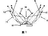
图7示出采用第二反光镜对光束从光源的中心范围的偏转;Figure 7 shows the deflection of the light beam from the center range of the light source using a second mirror;
图8示出采用第二反光镜对光束从光源的中心范围的偏转,其中沿照射条带的长度的光线聚焦的强度大于沿其宽度聚焦的强度;Figure 8 illustrates the deflection of the light beam from the central extent of the light source using a second mirror, where the light rays are focused with greater intensity along the length of the illuminated strip than along its width;
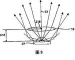
图9示出用凸透镜对来自中心范围的光线的聚焦;Figure 9 shows the focusing of rays from the central range with a convex lens;
图10示出用凸透镜对来自中心范围的光线的聚焦,其中沿照射条带的长度的光线聚焦的强度大于沿其宽度聚焦的强度;Figure 10 shows the focusing of light rays from the central region with a convex lens, where light rays are focused with greater intensity along the length of the illuminated strip than along its width;
图11示出用设置在前面的散射体实现两个相邻的光源的光线的至少部分的重叠;Fig. 11 shows the at least partial overlap of the light rays of two adjacent light sources with a diffuser arranged in front;
图12光学系统的侧视图;The side view of the optical system of Fig. 12;
图13示出设置在一个被冷却介质穿流的支座上的安装有光源的基片;Figure 13 shows a substrate with a light source installed on a support through which a cooling medium flows;
图14示出被冷却介质相互反向穿流的支座;Fig. 14 shows the supports through which the cooling medium flows in opposite directions;
图15示出用两个帕尔帖元件进行冷却的支座;Figure 15 shows a support cooled by two Peltier elements;
图16为行摄像机和光源的时间特性曲线;Fig. 16 is the time characteristic curve of line camera and light source;
图17为反射模件的立体图。Fig. 17 is a perspective view of a reflection module.
例如在印刷机中,优选在轮转印刷机中,特别是在采用胶印印刷工艺的印刷机中,一在图1中所示的材料03的表面在用箭头示出的移动方向04上移动。通过一例如设置在印刷机上例如在图中未示出的输送装置实现移动,其中在下面还将详细说明的光学系统工作时材料03优选仅在唯一一个移动方向04上移动,确切地说线性移动。被移动的材料03的速度是相同的或是可改变的。For example, in a printing press, preferably a rotary printing press, in particular a printing press using offset printing technology, the surface of a material 03 shown in FIG. 1 is moved in a direction of movement 04 indicated by an arrow. The movement takes place, for example, on a printing press with a conveying device, not shown in the figures, wherein the
材料03优选是平面的和扁平的,例如是单张纸03或是材料带03。材料03特别是由纸张构成的承印材料03,例如是有价证券03或纸币。材料03的表面02具有凸纹或通常突出于表面02的或作为下凹压入表面的结构,其中凸纹或结构的高度或深度与材料03的宽度B03相比非常小。至少一部分材料03的表面02例如通过附着反光的材料,例如漆或薄膜,通过嵌入窗线或在材料03上的另一种优选金属涂布形成反光结构。The
图2中仅示意示出的照明装置06在材料03的表面02上生成优选作为照射条带01的照射的图像01,所述照射条带具有长度L01和宽度B01(图1),其中宽度B01在材料03的表面02上垂直于长度L01延伸。照射条带01的宽度B01优选在材料03的移动方向04上定向,而照射条带01的长度L01优选平行于材料03的宽度B03定向和在材料03的部分宽度B03或在其整个宽度B03上延伸。照射条带01的宽度B01例如为3mm,优选为8mm。材料03的移动方向04因此优选至少基本平行于照射条带01的宽度B01定向,其中材料03的移动方向04在被照射条带01的长度L01和宽度B01展开的平面内。材料03优选至少在照射条带01的范围内不被拱形弯曲。The
照射装置06具有多个成行并列设置的光源07,从而使整个照射装置06成行状结构。照射装置06的成行设置的光源07优选平行于照射条带01的长度L01设置。光源07与材料03的表面02分别具有一个间距A07,其中所述间距A07优选在30mm至200mm之间,特别是在70mm至140mm之间。光源07的间距A07优选分别垂直于材料03的表面02。照射装置06的所有光源07优选结构相同,例如作为浅色的强光的发光二极管07或激光二极管07。在照明装置06内也可以设置多组分别具有多个成行并列设置的光源07,其中各组光源07的光学特性,例如由各组光源辐射的光线的波长不同。例如一组光源07辐射白色的光线,而另一组光源07辐射单色的光线。一个与照射装置06连接的控制装置23可以根据需要,例如根据材料03表面02的特性根据光线的颜色对各个光源07或光源07组进行选择和分别单独地以及相互独立地进行驱动,即有选择地激活。因此控制装置23可以对一组光源07独立于至少另一组光源07对其亮度和/或发光时间长度进行控制。而且还可以有选择地对单独的光源07或有选择地对光源07组进行激活,可以改变光源07生成的照明条带01的长度,以便以简单的方式使照明条带01的长度L01与例如有待照射的材料03的宽度B03适配。而且还可以在照明装置06的纵向上的材料03的表面仅照射选出的范围,其中照射的范围在照射装置06的纵向上被未被照射的或例如被其它颜色的光线照射的范围中断。其中照射条带01通常优选位于光源07辐射的光线的直接的或被偏转的光程内的焦点外面。The illuminating
照射装置06例如由多个行状的并列排列的模件M61-M65(图12)构成,所述模件分别具有多个行状并列设置的光源07,其中两个相邻的模件M61-M65之间的接缝26优选倾斜于照射条带01的长度L01设置。照射装置06的各个模件M61-M65的功能例如是相同的。例如一个与被照射的材料03的宽度B03相符的由多个并列排列的模件M61-M65组成的照射装置06的行的长度可以通过接通有关模件M61-M65的行状设置的光源07被激活。而且各个选出的模件M61-M65的光源07独立于其它模件M61-M65的光源07被激活。The illuminating
图3的两维图中示出照射装置06的单独的一个光源07。所述光源07将光线辐射到立体角ω内,其中立体角ω是一个对球截取的面AK,即展开的直至半球大小的球面AK。The two-dimensional representation in FIG. 3 shows a single
图4举例示出四个在图3中所示的光源07,所述光源成行状并列设置在一共同的基片21上。优选属于相应的光源07的电源22设置在同一基片21上。电源22优选是一个恒流电源22,特别是一个可控的恒流电源22。FIG. 4 shows an example of four
光学系统优选是设置在印刷机或对印刷产品继续加工的机器内或上的检查系统的组成部分并用于对印刷机生产的印刷品的质量进行判定,除了如图2所示的照射装置06外,至少还有一个采集装置08也属于所述的光学系统,所述采集装置08具有至少一个与材料03的表面02相距一个间隔A09设置的检测器09,其中检测器09对被材料03的表面02反射的光线进行采集。采集装置06例如是一个摄像机08,优选是一个行摄像机08,特别是彩色行摄像机08。而且采集装置08优选具有多个成行并列设置的检测器,其中成行设置的检测器09优选平行于照射装置01的长度和/或平行于材料03的宽度B03设置。在成行设置的检测器09的行之间存在的间隔优选与材料03的移动方向04具有相同的定向,即在材料03的移动方向04上前后顺序设置的检测器09行优选垂直于材料03的移动方向04设置。采集装置08的检测器09例如可以是CCD-阵列09或是一组光电二极管09。采集装置08的检测器09将采集的反射的光线转换成电信号并将电信号输送给一个与采集装置08连接的图像处理装置24,进行评价。The optical system is preferably an integral part of an inspection system arranged in or on a printing press or a machine for further processing of printed products and is used to determine the quality of the printed matter produced by the printing press, except for the illuminating
如图5所示,在光学系统中具有至少一个沿照射条带01的长度L01和/或沿照射条带01的宽度B01定向的作用面12的第一反光镜11与照射装置06的光源07配合,其中第一反光镜11的作用面12将从至少一个照射装置06的光源07辐射入立体角ω的光线限定在第一包面AH1上,所述第一包面AH1小于属于立体角ω的球面AK。第一反光镜11的作用面12可以是平的或下凹的。其中照射装置01至少一沿长度L01定向的第一反光镜11的作用面将照射装置06的一个光源07辐射到立体角ω内的光线较强地限定在第二包面AH2上,所述第二包面小于该第一反光镜11的至少一个沿照射装置01的宽度B01定向的作用面12,如图6对照如图5的光束所示。优选照射装置06的至少一个光源07具有第一反光镜11,所述第一反光镜具有至少两个对应于被光源07辐射的中心线13对称的作用面12。As shown in FIG. 5 , in the optical system there is at least one
如图7和8所示,例如设置有第二反光镜16,用于将来自照射装置06的至少一个光源07在环围中心线13的中心范围14辐射的射线进行偏转,其中其对环围至少一个在中心线13的光路环围的中心范围14内的作用面17设置在由光源07辐射的光线的立体角ω内,其中第二反光镜16的作用面17将至少照射装置06的光源07辐射的光线偏转向第一反光镜11的沿照射条带01的长度L01和/或宽度B01定向的作用面12上。其中光源07辐射的光线优选沿照射条带01的长度L01的聚焦强度大于沿其宽度B01的聚焦强度。且第二反光镜16的作用面17可以是平的或下凹的。在图7至10中分别用带有箭头的实线示出配属给中心范围14的由相应的光源07辐射的光线,与此相反用带有箭头的虚线示出由光源07在其相应的立体角ω内向周边辐射的光线。As shown in FIGS. 7 and 8 , for example, a
另外,与对由照射装置06的至少一个光源07在环围中心光线13的中心范围14内辐射的光线进行偏转相同,也可以如图9和10所示在环围中心光线13的光路的中心范围14在由照射装置06的至少一个光源07辐射的光线的立体角ω内设置有至少一个透镜18,特别是双凸透镜18,其中在光源07与透镜18的中心之间存在一个间距A18,其中所述间距A18优选小于光源07与材料03的表面02之间的间距A07一半。其中透镜18是旋转对称的,以便由光源07辐射的光线优选沿照射条带01的长度L01聚焦的强度大于沿其宽度B01聚焦的强度。In addition, in the same way as deflecting the light rays irradiated by at least one
如图11所示,照射装置06的光源07的优选设置应使照射装置06的至少两个相邻的光源07辐射的光线的相应的立体角ω或至少包面AH1;AH2至少在一个对照射条带01照射的分范围19内相互重叠。特别是当参与的相邻的光源07设置在两个相邻的模件M61-M65内时,将存在这种重叠。而且在图11还示出,在照射装置06的每个单独的光源07上至少沿照射装置01的宽度B01分别设有至少一个第一反光镜11,所述第一反光镜具有至少一个作用面12,优选具有两个相互对称的作用面12。As shown in Figure 11, the preferred setting of the
另外照射装置06在面向材料03的表面02的一侧,即在在照射装置06的出射侧具有一个散射体38,即对光线进行分散的体,例如一个圆柱镜或一个棱柱膜,其中散射体38将光源07向材料03的表面02辐射的光线优选仅沿照射条带01的长度L01分布或至少绝大部分沿照射条带01的长度L01分布。根据一优选实施方式,散射体38和照射装置06的至少一个反光镜11;16在唯一一个被称作反射模件39的构件内形成,其中优选一组例如5至10个成行并列设置的光源07将其光线分别辐射入沿该光源07行设置的反射模件39内。为此光源07设置在与光线出射面正相对的反射模件39的面上或此处甚至嵌入反射模件39内。反射模件39是一个例如由优选透明的塑料采用注塑工艺制成的构件。反射模件39因此优选特别是一个实心的型件,其中在所述型件上共同形成散射体38和和至少一个反射镜11;16,确切地说,在型件上没有将散射体38与至少一个反射镜11;16分隔开的与光学相关的界面。图17举例以立体图示出反射模件39,所述反射模件具有优选在光线出射面上集合在一体的散射体38,其中散射体38在反射模件39的出射面上例如为沟槽结构,即例如在型件上成型。优选用在照射装置06的纵向上延伸的下凹构成反射模件39,其中下凹将反射模件39的光线出射面分成两个优选相同宽度的分范围,其中反射模件39的光线出射面的至少一个分范围,优选每个分范围本身构成透镜,特别是凸透镜。反射模件39的光线出射面的至少一个分范围,优选每个分范围对在反射模件39的光线出射面上出射的光线流在在材料03的表面02上形成的照射条带01的方向上聚焦。反射模件39优选由多个并列排列的段构成,其中每个段形成由一个光源07馈送给反射模件39的光路。反射模件39优选安装在对光源07进行支撑的基片21上或安装在例如具有在反射模件39上形成的安装件41的支座27上。优选分别至少一个反射模件39与每个沿照射条带01的宽度B01设置的模件M61至M65配合。In addition, the illuminating
同样照射装置06的散射体38就对光源07辐射的光线的分布形成和均匀化其作用与反光镜11;16和/或透镜18的设置相同。散射体38特别用于实现对甚至在具有微结构的材料03的表面上的漫射的无阴影的照射,其中尽管光源07分别对材料03的表面02具有间隔A07但照射条带01仍可以同时形成非常亮的照射带。反光镜11;16和/或透镜18以及特别是散射体38的设置用于使光线可以从照射装置06以均匀的光线分布出射和因此即使在材料03的反射的表面02,例如在反射的漆、冷印章、窗线、贴片等上也不会使照射装置06的内部结构,即其各个光源07的设置成像,所以即使在相应的反射角的情况下进行观察也是看不见的。Likewise, the diffuser 38 of the illuminating
图12示出光学系统,其中从一个垂直于材料03的移动方向04的平面进行观察。照射装置06和对材料03的表面02照射的照射条带01相互间隔A07平行设置,但照射装置06的延伸,即其长度B06可以大于照射装置01的长度L01或大于材料03的宽度B03。照射装置06被分成多个模件M61-M65,即在本例中被分成五个成行并列设置的模件M61-M65,其中在每个模件M61-M65中设置的光源07分别将光线辐射到照射条带01上。由照射条带01反射的光线被距材料03的表面02的间距A09处设置的采集装置08的检测器09在沿照射条带01的长度L01展开的立体采集角α内进行采集,其中采集角α在本例中的大小应使检测器可以对被照射条带01在照射条带01的整个长度L01反射的光线进行采集。采集角α在材料03的表面02形成一个横截面,从而采集角α至少采集一部分被照射装置06辐射的光束的在照射条带01的宽度B01上延伸的横截面。被采集角α覆盖的横截面优选至少其大小与在材料03的表面02上被照射条带01的长度L01和宽度B01展开的面积相等。在材料03的移动方向04上照射装置06和采集装置08优选相互间隔设置,从而被照射装置06的光源07向材料03的表面02辐射的光线被材料03的表面02根据“入射角等于反射角”定律向采集装置08的检测器09反射。基于入射角预期的反射角根据材料03的表面02的特性,特别是根据其结构,特别是根据微结构将偏离上述的与完全反射的面的理想条件。FIG. 12 shows an optical system in which the observation is made from a plane perpendicular to the direction of movement 04 of the
由采集装置08对被照射条带01反射的光线摄取的图像的质量主要取决于照射装置06的光源07必须辐射恒定的光强度的光线。由于从光源07辐射的光线的光强度的变化导致在采集装置08内就输送给图像处理装置24的信号导致与被照射的材料03的表面02的特性的变化相同的结果,从而在图像处理装置24内可以对信号变化的原因不加区分。在此情况下由于在图像处理装置24中进行的图像评价不能得出关于被照射的材料03的表面的特性可信的结论。The quality of the image captured by the
一种辅助措施是将被照射装置06的光源辐射的光线的光线强度保持恒定。在照射装置06中采用的光源07优选是强光的发光二极管07或激光二极管07,其光强度与温度有关。在下面将对为了实现恒定的光强度在支座21上设置的光源07进行恒温的措施加以说明。所推荐的方案的优点在于光源的热负荷直接在产生位置被导出,从而可以实现很短的调整时间。An auxiliary measure is to keep the light intensity of the light irradiated by the light source of the illuminating
光源07优选设置在还安装有其它的电子器件的和具有电路的基片21上。发光二极管07或激光二极管07的半导体优选直接与基片21接触,所述基片例如是MCPCB(金属芯印刷电路板)或是具有由铝构成的芯的基片21,和在其对发光二极管07或激光二极管07进行支撑的安装面32上为形成尽可能小的热阻,在其导热的基板上仅具有一个非常薄的涂层。The
图13示出一种基片21,所述基片21具有多个成行设置的光源07,其中所述基片21本身设置在一支座27上,其中支座27优选在成行设置的光源07的下面的支座内部至少具有一个通道28,液体或气体冷却介质,例如水或空气对所述通道进行穿流。优选在支座27的端侧具有与前向流连接的开口29和与回流连接的开口31,其中冷却介质对支座27例如直线穿流。图14示出一种支座27,冷却介质在两个相反的方向穿流所述支座,从而在支座27上沿成行设置的光源07上实现均衡的温度图形。为此通道在支座27的一端上换向180°。FIG. 13 shows a
一在图中未示出的调整装置用于将在前向流的冷却介质的温度和穿流通道28的流量保持恒定。另外调整装置也可以将在前向流的冷却介质的温度与回流的冷却介质的温度之间的差保持恒定。因此冷却介质的绝对温度并不重要,重要的是不得超过由参与的材料的热阻得出的光源07的最大容许温度,由调整装置通过对温度的监视和基于对温度的监视做出的调整干预避免此点的发生。如果没有对温度和流量可调整的冷却介质供使用,也可以通过外部的与基片21连接的冷却器(图中未示出)实现对光源07的冷却。A regulating device (not shown in the figure) is used to keep the temperature of the cooling medium flowing forward and the flow rate through the
图15中示出采用流动的冷却介质的另一方案。安装有光源07的基片21设置在支座27上,其中支座27本身设置在至少一个帕尔帖器件33上,但优选设置在多个帕尔帖器件33上,其中帕尔帖器件33分别与一与支座27隔热的冷却体34连接。为实现通过图中未示出的电子调整装置对至少一个帕尔帖器件33进行调整,直接在支座27上通过一设置在支座上的温度传感器36进行必要的温度测量。当环境温度出现变化时,仅冷却体34的温度发生变化,而不是设置在基片21上的光源07的温度发生变化。电子调整装置可以集成在与照射装置06连接的控制装置23上。Another variant with a flowing cooling medium is shown in FIG. 15 . The
由于在印刷机上或在一对印刷品继续加工的机械上的移动的材料03以每秒几米的速度移动,例如以3米/秒或大于3米/秒的速度移动,其中例如在一单张纸印刷机中每小时将印刷15000个或多于15000个的印帖03和所述印帖穿过印刷机被输送,所以光学系统的设计应能实现对移动材料03的有效的摄像。其中要注意的是,在作为行摄像机08的采集装置08中根据移动材料03的速度被移动的材料03的表面反射的光线的采集量将发生变化。因此摄像的亮度也发生变化。在速度变化很大时,例如在所述机器中通常会出现此情况,所摄取的图像将不能被利用。Due to the moving
替代例如采用行摄像机08的采集装置的摄像,采用编译码器与移动的材料03的速度同步,建议照射装置06的各个光源07或一组光源07的接通时间t3与行摄像机08的触发,即曝光时间t1同步,其中照射装置优选被一由控制装置23控制的电源22,特别是恒流源驱动,从而移动的材料03的表面02与移动的材料03的速度无关始终被相同的光亮度照射。因此可以实现在很宽的移动的材料03的速度范围内被采集装置08,例如行摄像机08摄取的图像的相同的亮度,这是因为控制装置23将照射装置06的各个光源07或一组光源07的接通时间t3始终保持在小于行摄像机08的曝光时间t1的缘故。Instead of taking pictures of the acquisition device, for example with the
如上所述,优选在曝光装置06中设置有多组光源07,优选分别有至少一个电源22,特别是恒流源22与所述光源配合。光源07的接通时间t3通过与照射装置06连接的控制装置23,例如分组地相互独立地被相应的电源22驱动,从而可以在照射装置06的优选成行设置的光源07的长度上对光量度图形进行调整。优选沿照射条带01的长度L01进行的光量度图形的调整的优点是,可以通过一图中未示出的采集装置08,例如行摄像机08的光学装置对传输损耗进行补偿。As mentioned above, preferably multiple groups of
另外一例如与控制装置23连接的光传感器37可以对照射装置06的光源07的辐射的光量度进行测量,以便根据光传感器37的测量信号将通过控制装置23被电源22驱动的光源07的接通时间与例如光源07的衰减特性进行适配调整,并采用对光源07的驱动,例如对因老化导致的光量度的减少加以补偿。而且控制装置23还可以将光源07的接通时间t3例如与被照射的材料03的不同的光学特性进行适配调整,特别是自动地进行适配调整。Another
图16示出采集装置08,例如行摄像机08的时间特性曲线和照射装置06的光源07的时间特性曲线。行摄像机08根据上面的第一时间特性曲线在一定的时间点上被接通,从而在该时间点上行摄像机08的曝光时间t1开始。在曝光时间t1后紧接着是取决于移动材料03的速度的断开时间t2,所述断开时间位于两个在材料03的移动方向上先后相邻的摄像机08的图像行之间。至少一个根据对行摄像机08的控制触发的光源07如图16中中间的第二时间特性曲线通过被控制装置23控制的电源22与行摄像机08的曝光时间t1同步被驱动,其中在光源07接通的迟延时间t4后,即在物理条件决定的时间后直至光线辐射开始时,该光源在接通时间t3被保持接通状态,其中接通时间t3,优选由迟延时间t4和接通时间t3构成的和小于行摄像机08的曝光时间t1。行摄像机08和光源07的时间特性曲线以上述固定的相关性周期地进行重复。在图16中的下面的第三时间特性曲线作为与在接通时间t3触发的光源的比较示出恒定光源的接通时间t5的时间特性曲线。FIG. 16 shows the time characteristic curve of the
附图标记对照表 Reference Signs Comparison Table
01 图像,照射条带01 Image, illuminated strip
02 表面02 Surface
03 材料,单张纸,材料带,承印材料,有价证券,纸币03 Materials, sheets, tapes, printing materials, securities, banknotes
04 移动方向04 Direction of movement
05 -05 -
06 照射装置06 Irradiation device
07 光源,发光二极管,激光二极管07 Light source, light emitting diode, laser diode
08 采集装置,摄像机,行摄像机,彩色行摄像机08 Acquisition device, video camera, line camera, color line camera
09 检测器,CCD-阵列,光电二极管09 Detector, CCD-array, photodiode
10 -10 -
11 第一反光镜11 first mirror
12 作用面12 Acting surface
13 中心光线13 Center Ray
14 中心范围14 center range
15 -15 -
16 第二反光镜16 Second mirror
17 作用面17 Acting surface
18 透镜18 lens
19 分范围19 point range
20 -20 -
21 基片21 Substrate
22 电源,恒流电源22 Power supply, constant current power supply
23 控制装置23 control device
24 图像处理装置24 Image processing device
25 -25 -
26 接缝26 Seams
27 支座27 Support
28 通路28 access
29 开口29 opening
30 -30 -
31 开口31 opening
32 安装侧32 Installation side
33 帕尔帖器件33 Peltier device
34 冷却体34 cooling body
35 -35 -
36 温度传感器36 Temperature sensor
37 光传感器37 light sensor
38 散射体38 Scatterers
39 反射模件39 reflection module
40 -40 -
41 安装件41 Mounting parts
A07 间隔A07 Interval
A09 间隔A09 Interval
A18 间隔A18 Interval
B01 宽度B01 Width
B03 宽度B03 Width
B06 长度B06 Length
L01 长度L01 Length
Z18 中心Z18 center
AH1 第一包面AH1 The first bag of noodles
AH2 第二包面AH2 second bread
AK 面,球形表面AK surface, spherical surface
M61 模件M61 module
M62 模件M62 module
M63 模件M63 module
M64 模件M64 module
M65 模件M65 module
t1 曝光时间t1 exposure time
t2 断开时间t2 disconnection time
t3 接通时间t3 Turn-on time
t4 迟延时间t4 Delay time
t5 接通时间t5 Turn-on time
α 采集角α acquisition angle
ω 立体角ω solid angle
Claims (107)
Applications Claiming Priority (3)
| Application Number | Priority Date | Filing Date | Title |
|---|---|---|---|
| DE102004014541.5 | 2004-03-23 | ||
| DE102004014541ADE102004014541B3 (en) | 2004-03-23 | 2004-03-23 | Optical system e.g. for banknote checking device, inspection system or flat bed scanner, providing uniform intensity illumination strip on surface of moving material web |
| PCT/EP2005/051155WO2005093395A1 (en) | 2004-03-23 | 2005-03-15 | Optical system for creating an illuminating strip |
Publications (2)
| Publication Number | Publication Date |
|---|---|
| CN1957247Atrue CN1957247A (en) | 2007-05-02 |
| CN1957247B CN1957247B (en) | 2010-05-05 |
Family
ID=34399823
Family Applications (1)
| Application Number | Title | Priority Date | Filing Date |
|---|---|---|---|
| CN2005800166468AExpired - Fee RelatedCN1957247B (en) | 2004-03-23 | 2005-03-15 | Optical system for generating illumination strip |
Country Status (6)
| Country | Link |
|---|---|
| US (1) | US7682040B2 (en) |
| EP (1) | EP1730500B1 (en) |
| CN (1) | CN1957247B (en) |
| AT (1) | ATE366924T1 (en) |
| DE (2) | DE102004014541B3 (en) |
| WO (1) | WO2005093395A1 (en) |
Cited By (4)
| Publication number | Priority date | Publication date | Assignee | Title |
|---|---|---|---|---|
| CN106066330A (en)* | 2016-06-23 | 2016-11-02 | 昆山辉杰视自动化科技有限公司 | A kind of illuminator for line scanning and detecting system |
| CN106213904A (en)* | 2016-09-14 | 2016-12-14 | 浙江维融电子科技股份有限公司 | A kind of self-help bank sales counter |
| CN107850552A (en)* | 2015-06-02 | 2018-03-27 | 韩国生产技术研究院 | Optical Inspection Method for Carbon Fiber Reinforced Plastic Components |
| CN110778946A (en)* | 2019-11-18 | 2020-02-11 | 隋功然 | LED projection lamp device |
Families Citing this family (17)
| Publication number | Priority date | Publication date | Assignee | Title |
|---|---|---|---|---|
| JP2007013913A (en)* | 2005-05-30 | 2007-01-18 | Toyota Industries Corp | Lighting unit and original-reading apparatus |
| DE102005031957B4 (en) | 2005-07-08 | 2007-03-22 | Koenig & Bauer Ag | Apparatus for inspecting a substrate with non-uniform reflective surfaces |
| DE102005047913B3 (en) | 2005-10-06 | 2007-06-14 | Texmag Gmbh Vertriebsgesellschaft Gmbh | Device for emission of linear light |
| DE102006045626A1 (en)* | 2006-09-27 | 2008-04-03 | Giesecke & Devrient Gmbh | Device and method for the optical examination of value documents |
| DE102007009580A1 (en)* | 2007-02-26 | 2008-08-28 | Evonik Röhm Gmbh | Lighting device for use in scanner, sensor unit and attachment for detection of light-absorbing and light-diverting defects integrated in flat bed scanner, has transmitted light unit |
| DE102007014811A1 (en) | 2007-03-28 | 2008-10-09 | Rehau Ag + Co | Light-emitting arrangement |
| RU2402815C1 (en) | 2009-04-10 | 2010-10-27 | Общество С Ограниченной Ответственностью "Конструкторское Бюро "Дорс" (Ооо "Кб "Дорс") | Device for verification of banknotes |
| US20130284946A1 (en) | 2010-11-02 | 2013-10-31 | Kba-Notasys Sa | Device for irradiating substrate material in the form of a sheet or web and uses thereof |
| RU2447499C1 (en)* | 2010-12-21 | 2012-04-10 | Общество С Ограниченной Ответственностью "Конструкторское Бюро "Дорс" (Ооо "Кб "Дорс") | Device for measuring optical characteristics of document |
| DE102011002181A1 (en)* | 2011-04-19 | 2012-10-25 | Bundesdruckerei Gmbh | Method and device for checking security features in security documents |
| AT512200A1 (en)* | 2011-11-30 | 2013-06-15 | Ait Austrian Inst Technology | METHOD FOR RECORDING A LINE IMAGE |
| DE102012110793B4 (en)* | 2012-11-09 | 2020-09-03 | R.A.M. Realtime Application Measurement Gmbh | Device and method for imaging a web-shaped material |
| US8797611B2 (en) | 2012-12-12 | 2014-08-05 | Hewlett-Packard Development Company, L.P. | Illumination assembly |
| US9188733B2 (en) | 2013-06-07 | 2015-11-17 | Steelcase Inc. | Panel light assembly |
| DE102013221334A1 (en)* | 2013-10-21 | 2015-04-23 | Volkswagen Aktiengesellschaft | Method and measuring device for evaluating structural differences of a reflecting surface |
| US11442020B2 (en) | 2016-10-07 | 2022-09-13 | Hutchinson Technology Incorporated | On-axis and diffuse illumination for inspection systems |
| EP3748342B1 (en)* | 2019-06-06 | 2023-05-03 | Gebrüder Loepfe AG | Optical sensor for measuring a property of an elongate textile body in a uniform optical field |
Family Cites Families (28)
| Publication number | Priority date | Publication date | Assignee | Title |
|---|---|---|---|---|
| JPS6139771A (en) | 1984-07-31 | 1986-02-25 | Canon Inc | Image reader |
| US4972093A (en)* | 1987-10-09 | 1990-11-20 | Pressco Inc. | Inspection lighting system |
| JPH02535A (en)* | 1987-11-07 | 1990-01-05 | Minolta Camera Co Ltd | Thermal transfer color printer |
| JPH01255371A (en) | 1988-04-05 | 1989-10-12 | Fujitsu Ltd | System for driving light emitting diode |
| US5132791A (en)* | 1990-09-25 | 1992-07-21 | Ball Corporation | Optical sheet inspection system |
| DE4102122C2 (en) | 1990-12-08 | 1994-02-17 | Schoeller Felix Jun Papier | Method for visually checking the formation of a unidirectional web of photographic base paper or cardboard |
| EP0490097B1 (en)* | 1990-12-08 | 1997-03-26 | FELIX SCHOELLER JR. GMBH & CO. KG | Process for investigating transparent webs, especially photographic paper supports |
| JPH053527A (en) | 1991-06-25 | 1993-01-08 | Canon Inc | Adhesive image sensor |
| JPH06291939A (en)* | 1993-03-30 | 1994-10-18 | Toshiba Lighting & Technol Corp | Led light source device, reader and reader integrating device |
| DE4314219A1 (en) | 1993-04-30 | 1994-11-03 | Jenoptik Jena Gmbh | Arrangement for selective measurement of remission |
| DE4321177A1 (en) | 1993-06-25 | 1995-01-05 | Heidelberger Druckmasch Ag | Device for parallel image inspection and color control on a printed product |
| US5519496A (en)* | 1994-01-07 | 1996-05-21 | Applied Intelligent Systems, Inc. | Illumination system and method for generating an image of an object |
| DE19511782C2 (en) | 1995-03-30 | 1997-07-31 | Kurandt System Gmbh | Process for checking color printing originals and device for carrying out the process |
| DE19532877A1 (en)* | 1995-09-06 | 1997-03-13 | Giesecke & Devrient Gmbh | Device for linear lighting of sheet material, such as. B. banknotes or securities |
| US5713661A (en)* | 1995-10-23 | 1998-02-03 | Northeast Robotics, Inc. | Hockey puck shaped continuous diffuse illumination apparatus and method |
| US5936353A (en)* | 1996-04-03 | 1999-08-10 | Pressco Technology Inc. | High-density solid-state lighting array for machine vision applications |
| JPH09277593A (en)* | 1996-04-19 | 1997-10-28 | Oki Electric Ind Co Ltd | Light receiving and emitting element module and formation thereof |
| DE19617009C2 (en) | 1996-04-27 | 1999-05-20 | Roland Man Druckmasch | Photoelectric measuring device |
| US5690417A (en)* | 1996-05-13 | 1997-11-25 | Optical Gaging Products, Inc. | Surface illuminator with means for adjusting orientation and inclination of incident illumination |
| US5949584A (en)* | 1997-05-13 | 1999-09-07 | Northeast Robotics Llc | Wafer |
| US6022124A (en)* | 1997-08-19 | 2000-02-08 | Ppt Vision, Inc. | Machine-vision ring-reflector illumination system and method |
| US6473165B1 (en)* | 2000-01-21 | 2002-10-29 | Flex Products, Inc. | Automated verification systems and methods for use with optical interference devices |
| JP2002142082A (en)* | 2000-10-31 | 2002-05-17 | Pfu Ltd | Image reading device |
| DE10061070A1 (en) | 2000-12-08 | 2002-06-13 | Isra Vision Systems Ag | Elongated light source for use in inspection areas, particularly for examination of the surface of bands of cloth or material during production, with the length of the light source readily adjustable due to its modular design |
| JP3889992B2 (en)* | 2002-05-17 | 2007-03-07 | 株式会社ミツトヨ | Ring lighting device |
| DE20213431U1 (en) | 2002-08-31 | 2002-11-07 | MAN Roland Druckmaschinen AG, 63075 Offenbach | Equipment for quality control on printed matter |
| DE20303574U1 (en) | 2003-03-06 | 2003-04-30 | MAN Roland Druckmaschinen AG, 63075 Offenbach | Image inspection system for a printing press |
| DE102004003613B4 (en)* | 2004-01-25 | 2015-01-08 | grapho metronic Meß- und Regeltechnik GmbH | Apparatus for capturing an image from a predetermined portion of a moving piece of printed matter |
- 2004
- 2004-03-23DEDE102004014541Apatent/DE102004014541B3/ennot_activeWithdrawn - After Issue
- 2005
- 2005-03-15USUS10/594,092patent/US7682040B2/ennot_activeExpired - Fee Related
- 2005-03-15ATAT05731852Tpatent/ATE366924T1/enactive
- 2005-03-15DEDE502005001025Tpatent/DE502005001025D1/ennot_activeExpired - Lifetime
- 2005-03-15EPEP05731852Apatent/EP1730500B1/ennot_activeExpired - Lifetime
- 2005-03-15CNCN2005800166468Apatent/CN1957247B/ennot_activeExpired - Fee Related
- 2005-03-15WOPCT/EP2005/051155patent/WO2005093395A1/enactiveIP Right Grant
Cited By (5)
| Publication number | Priority date | Publication date | Assignee | Title |
|---|---|---|---|---|
| CN107850552A (en)* | 2015-06-02 | 2018-03-27 | 韩国生产技术研究院 | Optical Inspection Method for Carbon Fiber Reinforced Plastic Components |
| CN106066330A (en)* | 2016-06-23 | 2016-11-02 | 昆山辉杰视自动化科技有限公司 | A kind of illuminator for line scanning and detecting system |
| CN106213904A (en)* | 2016-09-14 | 2016-12-14 | 浙江维融电子科技股份有限公司 | A kind of self-help bank sales counter |
| CN106213904B (en)* | 2016-09-14 | 2022-02-22 | 维融科技股份有限公司 | Self-service bank counter |
| CN110778946A (en)* | 2019-11-18 | 2020-02-11 | 隋功然 | LED projection lamp device |
Also Published As
| Publication number | Publication date |
|---|---|
| DE102004014541B3 (en) | 2005-05-04 |
| CN1957247B (en) | 2010-05-05 |
| WO2005093395A1 (en) | 2005-10-06 |
| ATE366924T1 (en) | 2007-08-15 |
| EP1730500B1 (en) | 2007-07-11 |
| DE502005001025D1 (en) | 2007-08-23 |
| US7682040B2 (en) | 2010-03-23 |
| US20070188722A1 (en) | 2007-08-16 |
| EP1730500A1 (en) | 2006-12-13 |
Similar Documents
| Publication | Publication Date | Title |
|---|---|---|
| CN1957247A (en) | Optical system for generating illumination strips | |
| CN1933973A (en) | Optical system used to generate the illuminated image | |
| US6598994B1 (en) | Multi-angle inspection of manufactured products | |
| CN1185853C (en) | Multifunction Monitor Module for Printers | |
| US6286978B1 (en) | Light array system and method for illumination of objects imaged by imaging systems | |
| US8322872B2 (en) | Linear light diffusing structure for document scanners | |
| EP2773094B1 (en) | Lighting unit and image scanner using same | |
| CN101834970B (en) | Image reading apparatus | |
| CN103307492A (en) | LED condensation light source and material sorting device based on same | |
| US10571405B2 (en) | Quality control station for a sheet element processing machine and illumination unit for the quality control station | |
| JP3139822U (en) | Scanning device | |
| CN107702889A (en) | Linear light concentrator and optical detection apparatus | |
| JP2016092752A (en) | Light irradiation apparatus, image reading apparatus, and image forming apparatus | |
| JP2012160309A (en) | Light source unit and image reading device using the same | |
| JP2004191214A (en) | Line lighting system, and inspection device using line lighting system | |
| US20040009005A1 (en) | Image reading apparatus | |
| CN211786525U (en) | Linear condenser and optical detection device | |
| CA2584580A1 (en) | Container inspection by directly focusing a light emitting die element onto the container | |
| JP2005277879A (en) | Scanner light source unit | |
| JP2010166498A (en) | Lighting device and image reading device | |
| JP6162590B2 (en) | Line illumination device and image reading device | |
| JP2007201826A (en) | Image reading apparatus and image forming apparatus | |
| JP2005354511A (en) | Film scanner | |
| JP2005277158A (en) | Scanner light source unit |
Legal Events
| Date | Code | Title | Description |
|---|---|---|---|
| C06 | Publication | ||
| PB01 | Publication | ||
| C10 | Entry into substantive examination | ||
| SE01 | Entry into force of request for substantive examination | ||
| C14 | Grant of patent or utility model | ||
| GR01 | Patent grant | ||
| C17 | Cessation of patent right | ||
| CF01 | Termination of patent right due to non-payment of annual fee | Granted publication date:20100505 Termination date:20130315 |