CN1953035A - Gate pole driving circuit and liquid crystal display having the same - Google Patents
Gate pole driving circuit and liquid crystal display having the sameDownload PDFInfo
- Publication number
- CN1953035A CN1953035ACNA2006101359553ACN200610135955ACN1953035ACN 1953035 ACN1953035 ACN 1953035ACN A2006101359553 ACNA2006101359553 ACN A2006101359553ACN 200610135955 ACN200610135955 ACN 200610135955ACN 1953035 ACN1953035 ACN 1953035A
- Authority
- CN
- China
- Prior art keywords
- gate
- level
- signal
- shift register
- output
- Prior art date
- Legal status (The legal status is an assumption and is not a legal conclusion. Google has not performed a legal analysis and makes no representation as to the accuracy of the status listed.)
- Granted
Links
Images


Classifications
- G—PHYSICS
- G09—EDUCATION; CRYPTOGRAPHY; DISPLAY; ADVERTISING; SEALS
- G09G—ARRANGEMENTS OR CIRCUITS FOR CONTROL OF INDICATING DEVICES USING STATIC MEANS TO PRESENT VARIABLE INFORMATION
- G09G3/00—Control arrangements or circuits, of interest only in connection with visual indicators other than cathode-ray tubes
- G09G3/20—Control arrangements or circuits, of interest only in connection with visual indicators other than cathode-ray tubes for presentation of an assembly of a number of characters, e.g. a page, by composing the assembly by combination of individual elements arranged in a matrix no fixed position being assigned to or needed to be assigned to the individual characters or partial characters
- G09G3/34—Control arrangements or circuits, of interest only in connection with visual indicators other than cathode-ray tubes for presentation of an assembly of a number of characters, e.g. a page, by composing the assembly by combination of individual elements arranged in a matrix no fixed position being assigned to or needed to be assigned to the individual characters or partial characters by control of light from an independent source
- G09G3/36—Control arrangements or circuits, of interest only in connection with visual indicators other than cathode-ray tubes for presentation of an assembly of a number of characters, e.g. a page, by composing the assembly by combination of individual elements arranged in a matrix no fixed position being assigned to or needed to be assigned to the individual characters or partial characters by control of light from an independent source using liquid crystals
- G09G3/3611—Control of matrices with row and column drivers
- G09G3/3674—Details of drivers for scan electrodes
- G09G3/3677—Details of drivers for scan electrodes suitable for active matrices only
- G—PHYSICS
- G02—OPTICS
- G02F—OPTICAL DEVICES OR ARRANGEMENTS FOR THE CONTROL OF LIGHT BY MODIFICATION OF THE OPTICAL PROPERTIES OF THE MEDIA OF THE ELEMENTS INVOLVED THEREIN; NON-LINEAR OPTICS; FREQUENCY-CHANGING OF LIGHT; OPTICAL LOGIC ELEMENTS; OPTICAL ANALOGUE/DIGITAL CONVERTERS
- G02F1/00—Devices or arrangements for the control of the intensity, colour, phase, polarisation or direction of light arriving from an independent light source, e.g. switching, gating or modulating; Non-linear optics
- G02F1/01—Devices or arrangements for the control of the intensity, colour, phase, polarisation or direction of light arriving from an independent light source, e.g. switching, gating or modulating; Non-linear optics for the control of the intensity, phase, polarisation or colour
- G02F1/13—Devices or arrangements for the control of the intensity, colour, phase, polarisation or direction of light arriving from an independent light source, e.g. switching, gating or modulating; Non-linear optics for the control of the intensity, phase, polarisation or colour based on liquid crystals, e.g. single liquid crystal display cells
- G02F1/133—Constructional arrangements; Operation of liquid crystal cells; Circuit arrangements
- G—PHYSICS
- G09—EDUCATION; CRYPTOGRAPHY; DISPLAY; ADVERTISING; SEALS
- G09G—ARRANGEMENTS OR CIRCUITS FOR CONTROL OF INDICATING DEVICES USING STATIC MEANS TO PRESENT VARIABLE INFORMATION
- G09G3/00—Control arrangements or circuits, of interest only in connection with visual indicators other than cathode-ray tubes
- G09G3/20—Control arrangements or circuits, of interest only in connection with visual indicators other than cathode-ray tubes for presentation of an assembly of a number of characters, e.g. a page, by composing the assembly by combination of individual elements arranged in a matrix no fixed position being assigned to or needed to be assigned to the individual characters or partial characters
- G—PHYSICS
- G09—EDUCATION; CRYPTOGRAPHY; DISPLAY; ADVERTISING; SEALS
- G09G—ARRANGEMENTS OR CIRCUITS FOR CONTROL OF INDICATING DEVICES USING STATIC MEANS TO PRESENT VARIABLE INFORMATION
- G09G2300/00—Aspects of the constitution of display devices
- G09G2300/04—Structural and physical details of display devices
- G09G2300/0404—Matrix technologies
- G09G2300/0408—Integration of the drivers onto the display substrate
Landscapes
- Engineering & Computer Science (AREA)
- Physics & Mathematics (AREA)
- General Physics & Mathematics (AREA)
- Theoretical Computer Science (AREA)
- Computer Hardware Design (AREA)
- Crystallography & Structural Chemistry (AREA)
- Chemical & Material Sciences (AREA)
- Nonlinear Science (AREA)
- Mathematical Physics (AREA)
- Optics & Photonics (AREA)
- Control Of Indicators Other Than Cathode Ray Tubes (AREA)
- Liquid Crystal Display Device Control (AREA)
- Liquid Crystal (AREA)
- Shift Register Type Memory (AREA)
Abstract
Translated fromChinese
Description
Translated fromChinese相关申请的交叉参考Cross References to Related Applications
本申请要求于2005年10月18日提交的韩国专利申请No.10-2005-0098144的优先权,在此通过参考引用其整个内容。This application claims priority from Korean Patent Application No. 10-2005-0098144 filed on October 18, 2005, the entire contents of which are hereby incorporated by reference.
技术领域technical field
本发明涉及栅极驱动电路和带有该驱动电路的显示设备。更具体地说,本发明涉及用于使用每个都具有多级的多个移位寄存器来驱动多条栅极线的栅极驱动电路,以及具有该驱动电路的显示设备。The present invention relates to a gate drive circuit and a display device with the drive circuit. More specifically, the present invention relates to a gate driving circuit for driving a plurality of gate lines using a plurality of shift registers each having a plurality of stages, and a display device having the same.
背景技术Background technique
液晶显示器(LCD)是这样的设备:其中将电场施加到已经被注入到两个基板之间的具有各向异性介电常数的液晶物质,并且调整电场的强度以控制被传送到基板上的光量,以便可以在其上显示所期望的图像。A liquid crystal display (LCD) is a device in which an electric field is applied to a liquid crystal substance having an anisotropic dielectric constant that has been injected between two substrates, and the strength of the electric field is adjusted to control the amount of light transmitted to the substrates , so that the desired image can be displayed on it.
以这样的状态在这种LCD的基板上形成多条彼此平行的栅极线和横跨栅极线的多条数据线:栅极线和数据线彼此绝缘,并且将每个像素限定在由这些栅极线和数据线所包围的区域中。在各条栅极线和数据线彼此交叉的部分形成薄膜晶体管(下面称为“TFT”)和像素电极。A plurality of gate lines parallel to each other and a plurality of data lines straddling the gate lines are formed on a substrate of such an LCD in such a state that the gate lines and the data lines are insulated from each other, and each pixel is defined in a region defined by these In the area surrounded by gate lines and data lines. Thin film transistors (hereinafter referred to as "TFTs") and pixel electrodes are formed at portions where respective gate lines and data lines cross each other.
LCD包括用于驱动栅极线的栅极驱动电路和用于驱动数据线的源极驱动电路。如果栅极驱动电路将预定电压施加到栅极线,则分别连接到TFT的两端的数据线和像素电极彼此电连接。此时,源极驱动电路通过数据线施加预定的数据电压到像素电极,以便驱动LCD。The LCD includes a gate driving circuit for driving gate lines and a source driving circuit for driving data lines. If the gate driving circuit applies a predetermined voltage to the gate lines, the data lines and the pixel electrodes respectively connected to both ends of the TFT are electrically connected to each other. At this time, the source driving circuit applies a predetermined data voltage to the pixel electrode through the data line, so as to drive the LCD.
可以使用移位寄存器来驱动栅极驱动电路。A shift register can be used to drive the gate drive circuit.
图1示出了根据现有技术的构成LCD板的栅极驱动电路的移位寄存器的框图。FIG. 1 shows a block diagram of a shift register constituting a gate driving circuit of an LCD panel according to the related art.
该移位寄存器包括多个级21,其每一个包括用于驱动栅极线G1到G5的每一条的第一输出端GOUT、第二输出端SOUT、输入端IN、控制端CT、时钟输入端CK、地电压端VSS和驱动电压端VDD。The shift register comprises a plurality of
级21连接到每条栅极线而第二输出端SOUT连接到随后级的输入端IN和前面级的控制端CT两者,从而将级进行彼此依赖地连接以驱动所有的栅极线。A
为了在LCD上平滑地显示运动图像,应该每秒至少60次驱动栅极线。但是,因为如此配置的移位寄存器具有低操作速度,所以难于如通常所需要的那样驱动多至400条栅极线。In order to smoothly display moving images on the LCD, the gate lines should be driven at least 60 times per second. However, since the shift register thus configured has a low operation speed, it is difficult to drive as many as 400 gate lines as is generally required.
发明内容Contents of the invention
提供本发明的示例实施方式以解决上述问题。因此,本发明的示例实施方式提供用于使用每个都具有多级的多个移位寄存器来驱动多条栅极线的栅极驱动电路,以及具有该栅极驱动电路的显示设备。Example embodiments of the present invention are provided to solve the above-mentioned problems. Accordingly, example embodiments of the present invention provide a gate driving circuit for driving a plurality of gate lines using a plurality of shift registers each having a plurality of stages, and a display device having the same.
根据本发明的示例实施方式,提供用于将驱动信号输出到多条栅极线的栅极驱动电路,其包括用于分别驱动被分为p个组的栅极线的p个移位寄存器(其中p是3或3以上的任意自然数)。每个移位寄存器包括彼此依赖地连接的多个级,而且将开始信号输入到每个移位寄存器的第一级的输入端,并且将来自特定级的输出信号连接到每个移位寄存器的随后级的输入端,从而借助于相应级的输出信号来顺序驱动多条栅极线。According to an exemplary embodiment of the present invention, there is provided a gate driving circuit for outputting a driving signal to a plurality of gate lines including p shift registers ( wherein p is any natural number of 3 or more). Each shift register includes a plurality of stages connected dependently to each other, and a start signal is input to an input terminal of a first stage of each shift register, and an output signal from a specific stage is connected to an input terminal of each shift register. The input terminals of subsequent stages are used to sequentially drive a plurality of gate lines by means of output signals of corresponding stages.
将p个移位寄存器中所使用的p个开始信号彼此移位1/p。The p start signals used in the p shift registers are shifted by 1/p from each other.
每个级可以包括:输入端,用于接收之前级的任何一级中输出的级驱动信号;时钟端,用于接收彼此具有相位差的多个时钟信号中的任何一个时钟信号;控制端,用于接收随后级中的任何一级所输出的级驱动信号;第一输出端,用于输出级驱动信号。Each stage may include: an input terminal for receiving a stage driving signal output in any one of the previous stages; a clock terminal for receiving any one of a plurality of clock signals having a phase difference with each other; a control terminal, It is used to receive the stage driving signal output by any stage in the subsequent stages; the first output terminal is used to output the stage driving signal.
每个级可以还包括第二输出端,用于将级驱动信号输出到随后级的任何一级。Each stage may further include a second output for outputting a stage drive signal to any of the subsequent stages.
在该示例实施方式中,p是为4的自然数,而将栅极线分为以4n-3、4n-2、4n-1和4n(其中n是1或1以上的自然数)为顺序的四个组。In this exemplary embodiment, p is a natural number of 4, and the gate lines are divided into four groups in the order of 4n-3, 4n-2, 4n-1, and 4n (where n is a natural number of 1 or more). groups.
根据本发明的示例实施方式,提供一种显示设备,其包括:显示装置,其包括多条栅极线、与栅极线交叉的多条数据线以及形成在栅极线和数据线之间的开关元件和像素电极;栅极驱动电路,用于选择栅极线和允许连接到所选择的栅极线的开关元件被导通;以及源极驱动电路,用于通过开关元件根据输入的图像数据的导通来驱动连接到像素电极的数据线。栅极驱动电路包括用于分别驱动被分为p个组的栅极线的p个移位寄存器(其中p是3或3以上的任意自然数),每个移位寄存器包括彼此依赖地连接的多个级,并且将开始信号输入到每个移位寄存器的第一级的输入端,而且将来自特定级的输出信号连接到每个移位寄存器的随后级的输入端,从而借助于相应级的输出信号来顺序驱动多条栅极线。According to an exemplary embodiment of the present invention, there is provided a display apparatus including: a display device including a plurality of gate lines, a plurality of data lines intersecting the gate lines, and a display device formed between the gate lines and the data lines. a switching element and a pixel electrode; a gate driving circuit for selecting a gate line and allowing a switching element connected to the selected gate line to be turned on; and a source driving circuit for using the switching element according to input image data conduction to drive the data line connected to the pixel electrode. The gate drive circuit includes p shift registers (where p is an arbitrary natural number of 3 or more) for respectively driving gate lines divided into p groups, and each shift register includes a plurality of mutually dependently connected stages, and the start signal is input to the input of the first stage of each shift register, and the output signal from the particular stage is connected to the input of the subsequent stage of each shift register, thereby by means of the corresponding stage's Output signals to sequentially drive multiple gate lines.
将在p个移位寄存器中所使用的p开始信号彼此移位1/p。The p start signals used in the p shift registers are shifted by 1/p from each other.
每个级可以包括:输入端,用于接收之前级的任何一级所输出的级驱动信号;时钟端,用于接收彼此具有相位差的多个时钟信号中的任何一个时钟信号;控制端,用于接收随后级的任何一级所输出的级驱动信号;第一输出端,用于输出栅极驱动信号。Each stage may include: an input end for receiving a stage drive signal output by any stage of the preceding stage; a clock end for receiving any one of a plurality of clock signals having a phase difference with each other; a control end for It is used to receive the stage drive signal output by any stage of the subsequent stage; the first output terminal is used to output the gate drive signal.
每个级还可以包括第二输出端,用于将级驱动信号输出到随后级的任何一级。Each stage may also include a second output for outputting a stage drive signal to any subsequent stage.
在本示例实施方式中,p是为4的自然数,而将栅极线分为以4n-3、4n-2、4n-1和4n(其中n是1或1以上的自然数)为顺序的四个组。In this exemplary embodiment, p is a natural number of 4, and the gate lines are divided into four groups in the order of 4n-3, 4n-2, 4n-1, and 4n (where n is a natural number of 1 or more). groups.
源极驱动电路在由栅极信号施加到栅极线时的时间段除以p所获得的p个时间端中的最后时间段中施加数据电压。The source driving circuit applies the data voltage in the last time period among p time terminals obtained by dividing the time period when the gate signal is applied to the gate line by p.
附图说明Description of drawings
通过结合附图进行的下面描述,将更加详细地理解本发明的示例实施方式,其中:Exemplary embodiments of the present invention will be understood in more detail from the following description taken in conjunction with the accompanying drawings, in which:
图1示出了根据现有技术构成液晶显示器(LCD)板的栅极驱动电路的移位寄存器的框图;1 shows a block diagram of a shift register constituting a gate drive circuit of a liquid crystal display (LCD) panel according to the prior art;
图2示出了根据本发明示例实施方式的LCD的示意图;Figure 2 shows a schematic diagram of an LCD according to an example embodiment of the present invention;
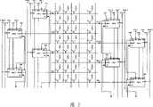
图3示出了构成根据本发明示例实施方式的LCD板的驱动电路的移位寄存器的框图;3 shows a block diagram of a shift register constituting a driving circuit of an LCD panel according to an exemplary embodiment of the present invention;
图4示出了施加到图3中所示的移位寄存器和栅极线的电压的波形图;和FIG. 4 shows waveform diagrams of voltages applied to the shift register and gate lines shown in FIG. 3; and
图5示出了在图3中所示的移位寄存器中的每一级的内部电路的电路图。FIG. 5 shows a circuit diagram of an internal circuit of each stage in the shift register shown in FIG. 3 .
具体实施方式Detailed ways
图2示出了根据本发明的示例实施方式的液晶显示器(LCD)的示意图。FIG. 2 shows a schematic diagram of a liquid crystal display (LCD) according to an example embodiment of the present invention.
如图2所示,根据本发明示例实施方式的LCD包括LCD板100、栅极驱动电路200、源极驱动电路300、驱动电压产生器400、定时控制器500和灰度级电压产生器600。As shown in FIG. 2 , an LCD according to an exemplary embodiment of the present invention includes an
LCD板100包括在行方向中形成的多条栅极线G1、G2、...、和G4n以及在列方向中形成的多条数据线D1、D2、...、Dm。将像素限定在由栅极线和数据线包围的区域中。像素包括连接到栅极线和数据线的薄膜晶体管(下面称为“TFT”)以及像素电极。这里,n和m是1或1以上的自然数。The
如果栅极驱动电路200将预定电压施加到栅极线,则分别连接到TFT的两端的数据线和像素电极彼此电连接。此时,源极驱动电路300通过数据线将预定数据电压施加到像素电极,以便驱动LCD板100。If the
定时控制器500从LCD模块之外的图形控制器(未示出)接收红(R)、绿(G)、蓝(B)数据信号、作为帧排序信号工作的垂直同步信号Vsync、水平同步信号Hsync和主时钟信号CLK,以产生和输出用于驱动栅极和源极驱动电路200和300的数字信号。
从定时控制器500输出到栅极驱动电路200的定时信号包括诸如用于指令开始施加栅极信号到栅极线的垂直开始信号、用于顺序施加栅极信号到每条栅极线的栅极时钟信号和用于允许栅极驱动电路200的输出被使能的栅极导通信号(gate on signal)之类的控制信号。Timing signals output from the
从定时控制器500输出到源极驱动电路300的定时信号包括诸如用于指令开始驱动从图形控制器接收到的RGB数据信号的水平开始信号、用于指令在源极驱动电路300中施加转换为模拟信号的数据信号的信号以及用于在源极驱动电路300中移位数据的水平时钟信号之类的控制信号。The timing signal output from the
驱动电压产生器400产生其每一个都被用作栅极信号的栅极导通(gate-on)和栅极截止(gate-off)电压Von和Voff、以及当产生灰度级电压时作为参考的驱动参考电压AVdd和公共电压Vcom。将栅极导通和栅极截止电压Von和Voff输出到栅极驱动电路200,而且将驱动参考电压AVdd输出到公共电压产生器(未示出)和灰度级电压产生器600。The
此时,栅极驱动电路200从定时控制器500接收栅极时钟信号和垂直开始信号,从驱动电压产生器400接收栅极驱动电压Von和Voff,并且控制器相关TFT,从而将数据电压发送到在LCD板100上的每个相关像素。At this time, the
根据本发明示例实施方式的驱动电路200使用每一个都具有多级的第一到第四移位寄存器来将栅极导通电压Von顺序地施加到栅极线G1、G2、...、G4n,从而允许LCD板的TFT被导通或者截止。The
第一移位寄存器驱动第(4n-3)条栅极线G1、G5、...、和G4n-3;第二移位寄存器驱动第(4n-2)条栅极线G2、G6、...、和G4n-2;第三移位寄存器驱动第(4n-1)条栅极线G3、G7、...、和G4n-1;而第四移位寄存器驱动第(4n)条栅极线G4、G8、...、和G4n。也就是说,栅极驱动电路200使用四个相关移位寄存器来驱动被分类为四个组G1、G2、...、和G4n中的栅极线。The first shift register drives the (4n-3) gate lines G1, G5, ..., and G4n-3; the second shift register drives the (4n-2) gate lines G2, G6, . .., and G4n-2; the third shift register drives the (4n-1)th gate line G3, G7, ..., and G4n-1; and the fourth shift register drives the (4n)th gate line Polar lines G4, G8, . . . , and G4n. That is, the
栅极驱动电路200形成在LCD板100的边缘区域中,更具体地说,形成在LCD板100上不形成像素的非显示区域的两侧处。在本示例实施方式中,将四个移位寄存器的两个移位寄存器排列在一侧而将另外两个移位寄存器排列在另外一侧。而且,当形成LCD板的像素时还可以一同形成栅极驱动电路200。The
灰度级电压产生器600根据从图形控制器接收来的RGB数据的比特数来产生灰度级电压,并且将所产生的灰度级电压发送到源极驱动电路300。The
源极驱动电路300根据从定时控制器500输出的信号将数据电压施加到数据线D1、D2、...、和Dm。The
图3示出了构成图2中所示的LCD板的栅极驱动电路的第一到第四移位寄存器的框图,而图4示出了施加到图3中所示的移位寄存器的电压的波形图。FIG. 3 shows a block diagram of first to fourth shift registers constituting the gate drive circuit of the LCD panel shown in FIG. 2, and FIG. 4 shows voltages applied to the shift registers shown in FIG. waveform diagram.
参照图3,图2的栅极驱动电路200包括带有彼此依赖地连接的多个第一级210(SCR1)的第一移位寄存器;带有彼此依赖地连接的多个第二级220(SCR2)的第二移位寄存器;带有彼此依赖地连接的多个第三级230(SCR3)的第三移位寄存器;和带有彼此依赖地连接的多个第四级240(SCR4)的第二移位寄存器;第一移位寄存器连接到第(4n-3)条栅极线G1、G5、...、和G4n-3;第二移位寄存器连接到第(4n-2)条栅极线G2、G6、...、和G4n-2;第三移位寄存器连接到第(4n-1)条栅极线G3、G7、...、和G4n-1;而第四移位寄存器连接到第(4n)条栅极线G4、G8、...、和G4n。Referring to FIG. 3, the
移位寄存器的每一级包括输入端IN、第一输出端GOUT、第二输出端SOUT、控制端CT、时钟输入端CK、地电压端VSS和驱动电压端VDD。Each stage of the shift register includes an input terminal IN, a first output terminal GOUT, a second output terminal SOUT, a control terminal CT, a clock input terminal CK, a ground voltage terminal VSS and a driving voltage terminal VDD.
将开始信号输入到包括在移位寄存器中的第一级的输入端IN。而且,将每一级的第二输出端SOUT连接到相关移位寄存器的随后级的输入端IN以及其之前级的控制端,从而这些级彼此依赖地连接。A start signal is input to the input terminal IN of the first stage included in the shift register. Furthermore, the second output SOUT of each stage is connected to the input IN of the subsequent stage of the associated shift register and the control terminal of the stage preceding it, so that these stages are connected dependently on each other.
将第一开始信号STV_1输入到第一移位寄存器中的第一级的输入端IN。将每一级的第一输出端GOUT连接到与其对应的每条栅极线G1、G5、...、和G4n-3。将第一时钟信号CKV_1提供给奇数级而将第一反时钟信号CKVB_1提供给偶数级。此时,第一时钟信号CKV_1和第一反时钟信号CKVB_1具有彼此相反的相位。The first start signal STV_1 is input to the input terminal IN of the first stage in the first shift register. The first output terminal GOUT of each stage is connected to each gate line G1, G5, . . . , and G4n-3 corresponding thereto. The first clock signal CKV_1 is provided to odd stages and the first inverted clock signal CKVB_1 is provided to even stages. At this time, the first clock signal CKV_1 and the first inverted clock signal CKVB_1 have phases opposite to each other.
将第二开始信号STV_2输入到第二移位寄存器中的第一级的输入端IN。将每一级的第一输出端GOUT连接到与其对应的每条栅极线G2、G6、...、和G4n-2。将第二时钟信号CKV_2提供给奇数级而将第二反时钟信号CKVB_2提供给偶数级。此时,第二时钟信号CKV_2和第二反时钟信号CKVB_2具有彼此相反的相位。The second start signal STV_2 is input to the input terminal IN of the first stage in the second shift register. The first output terminal GOUT of each stage is connected to each gate line G2, G6, . . . , and G4n-2 corresponding thereto. The second clock signal CKV_2 is provided to the odd stages and the second inverted clock signal CKVB_2 is provided to the even stages. At this time, the second clock signal CKV_2 and the second inverted clock signal CKVB_2 have phases opposite to each other.
将第三开始信号STV_3输入到第三移位寄存器中的第一级的输入端IN。将每一级的第一输出端GOUT连接到与其对应的每条栅极线G3、G7、...、和G4n-1。将第三时钟信号CKV_3提供给奇数级而将第三反时钟信号CKVB_3提供给偶数级。此时,第三时钟信号CKV_3和第三反时钟信号CKVB_3具有彼此相反的相位。The third start signal STV_3 is input to the input terminal IN of the first stage in the third shift register. The first output terminal GOUT of each stage is connected to each gate line G3, G7, . . . , and G4n-1 corresponding thereto. The third clock signal CKV_3 is provided to the odd stages and the third inverted clock signal CKVB_3 is provided to the even stages. At this time, the third clock signal CKV_3 and the third inverted clock signal CKVB_3 have phases opposite to each other.
将第四开始信号STV_4输入到第四移位寄存器中的第一级的输入端IN。将每一级的第一输出端GOUT连接到与其对应的每条栅极线G4、G8、...、和G4n。将第四时钟信号CKV_4提供给奇数级而将第四反时钟信号CKVB_4提供给偶数级。此时,第四时钟信号CKV_4和第四反时钟信号CKVB_4具有彼此相反的相位。The fourth start signal STV_4 is input to the input terminal IN of the first stage in the fourth shift register. The first output terminal GOUT of each stage is connected to each gate line G4, G8, . . . , and G4n corresponding thereto. The fourth clock signal CKV_4 is provided to the odd stages and the fourth inverted clock signal CKVB_4 is provided to the even stages. At this time, the fourth clock signal CKV_4 and the fourth inverted clock signal CKVB_4 have phases opposite to each other.
在移位寄存器中,将随后级的输出信号作为控制信号输入到当前级的控制端CT。此时,输入到控制端CT的控制信号进行工作以将相关级的输出信号向下改变到低状态。以这种方式,顺序地将第一到第四移位寄存器的输出信号设置在高状态,从而可以顺序地驱动栅极线G1到G4n。In the shift register, the output signal of the subsequent stage is input as a control signal to the control terminal CT of the current stage. At this time, the control signal input to the control terminal CT operates to change the output signal of the relevant stage down to a low state. In this way, the output signals of the first to fourth shift registers are sequentially set in a high state, so that the gate lines G1 to G4n can be sequentially driven.
下面将参照图4来详细描述根据本发明示例实施方式的栅极驱动电路的操作。The operation of the gate driving circuit according to an example embodiment of the present invention will be described in detail below with reference to FIG. 4 .
参照图4,在根据本发明的实施方式的第二到第四移位寄存器中所分别使用的第二到第四开始信号是相对于第一开始信号被顺序移位1/4长度的信号。也就是说,第二开始信号是将第一开始信号移位1/4的长度的信号;第三开始信号是将第二开始信号移位1/4的长度的信号;而第四开始信号是将第三开始信号移位1/4的长度的信号。Referring to FIG. 4 , second to fourth start signals respectively used in the second to fourth shift registers according to an embodiment of the present invention are signals sequentially shifted by 1/4 length with respect to the first start signal. That is to say, the second start signal is a signal shifted by the length of 1/4 of the first start signal; the third start signal is a signal of shifted length of 1/4 of the second start signal; and the fourth start signal is A signal that shifts the third start signal by 1/4 of the length.
与第一到第四开始信号类似,第一到第四时钟信号和第一到第四反时钟信号具有这样的关系:第二到第四时钟信号和反时钟信号相对于第一时钟信号和反时钟信号分别顺序移位1/4长度。因此,从第二到第四移位寄存器中输出的栅极信号也相对于从第一移位寄存器输出的栅极信号被顺序移位1/4长度。Similar to the first to fourth start signals, the first to fourth clock signals and the first to fourth inverted clock signals have such a relationship that the second to fourth clock signals and inverted clock signals are relative to the first clock signal and inverted clock signal. The clock signals are sequentially shifted by 1/4 length respectively. Therefore, the gate signals output from the second to fourth shift registers are also sequentially shifted by 1/4 length with respect to the gate signals output from the first shift register.
也就是说,根据本发明示例实施方式的栅极驱动电路200将输出到第一到第八条线G1到G8的栅极信号相对于输出到第一栅极线G1的信号移位1/4长度。That is, the
将参照图4来讨论时间段①。在图4中所示的时间段①中,将用于驱动与第一栅极线G1对应的像素的数据电压D1输出到数据线D1到Dm。此时,由于将栅极信号输出到第一至第四栅极线G1至G4,所以在与第一到第四栅极线G1到G4对应的四条线的像素中充电有数据电压D1。因此,与第一到第四栅极线G1到G4对应的四条线的像素具有彼此相同的数据电压。
随后,将讨论时间段②。由于在时间段②内切断第一栅极线G1的栅极信号,所以维持数据电压D1如同在与第一栅极线G1对应的相关像素中一样。Subsequently,
而且,在时间段②中,将用于驱动与第二栅极线G2对应的像素的数据电压D2输出到数据线D1到Dm。此时,由于将栅极信号输出到第二至第五栅极线G2到G5,所以在与第二到第五栅极线G2到G5对应的四条线的像素中充电数据电压D2。因此,与第二到第五栅极线G2到G5对应的四条线的像素具有彼此相同的数据电压。Also, in the
随后,将讨论时间段③。由于在时间段③中切断第二栅极线G2的栅极信号,所以维持数据电压D2如同在与第二栅极线G2对应的相关像素中一样。Subsequently, the time period ③ will be discussed. Since the gate signal of the second gate line G2 is cut off in the period ③, the data voltage D2 is maintained as in the relevant pixel corresponding to the second gate line G2.
而且,在时间段③中,将用于驱动与第三栅极线G3对应的像素的数据电压D3输出到数据线D1到Dm。此时,由于将栅极信号输出到第三到第六栅极线G3到G6,所以在与第三到第六栅极线G3到G6对应的四条线的像素中充电有数据电压D3。因此,与第三到第六栅极线G3到G6对应的四条线的像素具有彼此相同的数据电压。Also, in the period ③, the data voltage D3 for driving the pixel corresponding to the third gate line G3 is output to the data lines D1 to Dm. At this time, since the gate signal is output to the third to sixth gate lines G3 to G6, pixels of four lines corresponding to the third to sixth gate lines G3 to G6 are charged with the data voltage D3. Accordingly, pixels of four lines corresponding to the third to sixth gate lines G3 to G6 have the same data voltage as each other.
以这样的方式,在时间段④到⑧中分别施加数据电压D4到D8,在与第四到第八栅极线G4到G8对应的像素中分别充电有数据电压D4到D8。In this way, the data voltages D4 to D8 are respectively applied in the
也就是说,将根据本发明示例实施方式的LCD以这样的方式进行配置:将其中把栅极信号施加到栅极线G1到G4n的时间段四等分,而且在所分的时间段的随后时间段中施加数据电压,从而可以在与相关栅极线对应的像素中充电数据电压。That is, the LCD according to the exemplary embodiment of the present invention is configured in such a manner that the time period in which the gate signal is applied to the gate lines G1 to G4n is quartered, and after the divided time period The data voltage is applied during the time period, so that the data voltage can be charged in the pixel corresponding to the relevant gate line.
如果使用这样的栅极驱动电路,其可以驱动是只使用一个移位寄存器的栅极驱动电路所驱动的栅极线四倍的栅极线。If such a gate driving circuit is used, it can drive four times as many gate lines as a gate driving circuit using only one shift register.
虽然已经描述了在根据本发明示例实施方式的栅极驱动电路中使用四个移位寄存器,但是可以使用p个移位寄存器将栅极线分为p个组,而且可以使用移位了1/p的信号驱动p倍的栅极线(其中p是3或3以上的任意自然数)。Although it has been described that four shift registers are used in the gate driving circuit according to the exemplary embodiment of the present invention, p shift registers may be used to divide gate lines into p groups, and a shift of 1/ The p signal drives p times the gate lines (where p is any natural number of 3 or more).
下面,将描述构成移位寄存器的级的内部电路。虽然在上述移位寄存器中存在有执行相同操作的各种电路,但是将以例子的方式仅仅描述在该电路中经常使用的一种电路。Next, the internal circuits constituting the stages of the shift register will be described. Although there are various circuits that perform the same operation in the shift register described above, only one circuit that is often used among such circuits will be described by way of example.
图5示出了包括在移位寄存器中的每个级的内部电路的电路图。FIG. 5 shows a circuit diagram of an internal circuit of each stage included in the shift register.
参照图5,每个级包括第一上拉单元251、第二上拉单元252、第一下拉单元253、第二下拉单元254、上拉驱动单元255和下拉驱动单元256。Referring to FIG. 5 , each stage includes a first pull-up
第一上拉单元251将提供给时钟端CK的信号作为栅极驱动信号输出到第一输出端GOUT。第二上拉单元252将提供给时钟端CK的信号作为级驱动信号输出到第二输出端SOUT。The first pull-up
第一上拉单元251包括第一晶体管NT1,其中栅极电极、源极电极和漏极电极分别连接到第一节点N1、时钟端CK和第一输出端GOUT。第二上拉单元252包括第二晶体管NT2,其中栅极电极、源极电极和漏极电极分别连接到第一节点N1、时钟端CK和第二输出端SOUT。The first pull-up
在已经将第一上拉单元251截止之后,将第一下拉单元253导通以将输出到第一输出端GOUT的栅极驱动信号放电,而且将第二下拉单元254导通以将输出到第二输出端SOUT的级驱动信号放电。After the first pull-up
第一下拉单元253包括第三晶体管NT3,其中栅极电极、源极电极和漏极电极分别连接到第二节点N2、第一输出端GOUT和地电压端VSS。第二下拉单元252包括第四晶体管NT4,其中栅极电极、源极电极和漏极电极分别连接到第二节点N2、第二输出端SOUT和地电压端VSS。The first pull-down
上拉驱动单元255包括第五到第七晶体管NT5、NT6和NT7以导通第一和第二上拉单元251和252。The pull-up
以这样的方式来配置第五晶体管NT5:将栅极电极、漏极电极和源极电极分别连接到输入端IN、驱动电压端VDD和第一节点N1。以这样的方式来配置第六晶体管NT6:将栅极和漏极电极连接到驱动电压端VDD而将源极电极连接到第三节点N3。以这样的方式来配置第七晶体管NT7:将栅极电极、漏极电极和源极电极分别连接到第一节点N1、第三节点N3和地电压端VSS。The fifth transistor NT5 is configured in such a manner that the gate electrode, the drain electrode, and the source electrode are connected to the input terminal IN, the driving voltage terminal VDD, and the first node N1, respectively. The sixth transistor NT6 is configured in such a manner that the gate and drain electrodes are connected to the drive voltage terminal VDD and the source electrode is connected to the third node N3. The seventh transistor NT7 is configured in such a manner that the gate electrode, the drain electrode, and the source electrode are respectively connected to the first node N1, the third node N3, and the ground voltage terminal VSS.
下拉驱动单元256包括第八到第十二晶体管NT8、NT9、NT10、NT11和NT12,以导通第一和第二下拉单元253和254,同时截止第一和第二上拉单元251和252。The pull-down
以这样的方式来配置第八晶体管NT8:将栅极电极、漏极电极和源极电极分别连接到第三节点N3、驱动电压端VDD和第二节点N2。以这样的方式来配置第九晶体管NT9:将栅极电极、漏极电极和源极电极分别连接到第一节点N1、第二节点N2和地电压端VSS。以这样的方式来配置NT10:将栅极电极、漏极电极和源极电极分别连接到输入端IN、第二节点N2和地电压端VSS。The eighth transistor NT8 is configured in such a manner that the gate electrode, the drain electrode, and the source electrode are respectively connected to the third node N3, the driving voltage terminal VDD, and the second node N2. The ninth transistor NT9 is configured in such a manner that the gate electrode, the drain electrode, and the source electrode are respectively connected to the first node N1, the second node N2, and the ground voltage terminal VSS. The NT10 is configured in such a manner that the gate electrode, the drain electrode and the source electrode are respectively connected to the input terminal IN, the second node N2 and the ground voltage terminal VSS.
以这样的方式来配置第十一晶体管NT11:将栅极电极、漏极电极和源极电极分别连接到第二节点N2、第一节点N1和地电压端VSS。以这样的方式来配置第十二晶体管NT12:将栅极电极、漏极电极和源极电极分别连接到控制端CT、第一节点N1和地电压端VSS。The eleventh transistor NT11 is configured in such a manner that a gate electrode, a drain electrode, and a source electrode are respectively connected to the second node N2, the first node N1, and the ground voltage terminal VSS. The twelfth transistor NT12 is configured in such a manner that a gate electrode, a drain electrode, and a source electrode are connected to the control terminal CT, the first node N1, and the ground voltage terminal VSS, respectively.
如果将从之前级的第二输出端SOUT输出的级驱动信号提供给输入端IN,则将第五晶体管NT5导通,从而第一节点N1的电势逐渐增加。随着第一节点N1的电势增加,将第一和第二晶体管NT1和NT2导通,从而将栅极和级驱动信号分别输出到第一和第二输出端GOUT和SOUT。If the stage driving signal output from the second output terminal SOUT of the previous stage is supplied to the input terminal IN, the fifth transistor NT5 is turned on so that the potential of the first node N1 gradually increases. As the potential of the first node N1 increases, the first and second transistors NT1 and NT2 are turned on, thereby outputting gate and stage driving signals to the first and second output terminals GOUT and SOUT, respectively.
同时,因为在将第六晶体管总维持在导通状态中第一节点N1的电势升高,所以如果将第七晶体管NT7导通则第三节点N3的电势下降。Meanwhile, since the potential of the first node N1 rises in always maintaining the sixth transistor in the on state, the potential of the third node N3 falls if the seventh transistor NT7 is turned on.
因为第三节点N3的电势下降,所以第八晶体管NT8维持在截止状态。因此,不将驱动电压提供给第二节点N2。而且,当第一节点N1的电势升高而且因此将第三和第四晶体管NT3和NT4截止时,将第九晶体管NT9导通以将第二节点N2的电势维持在地电压。Since the potential of the third node N3 falls, the eighth transistor NT8 is maintained in an off state. Therefore, the driving voltage is not supplied to the second node N2. Also, when the potential of the first node N1 rises and thus the third and fourth transistors NT3 and NT4 are turned off, the ninth transistor NT9 is turned on to maintain the potential of the second node N2 at the ground voltage.
之后,如果提供通过控制端CT从随后级的第二输出端SOUT输出的级驱动信号,则将第十二晶体管N12导通以将第一节点N1的电势放电到地电压端VSS。因为第一节点N1的电势下降,所以第七和第九晶体管NT7和NT9截止。After that, if the stage driving signal output from the second output terminal SOUT of the subsequent stage through the control terminal CT is supplied, the twelfth transistor N12 is turned on to discharge the potential of the first node N1 to the ground voltage terminal VSS. Since the potential of the first node N1 falls, the seventh and ninth transistors NT7 and NT9 are turned off.
因此,第二节点N2的电势逐渐上升,从而第三和第四晶体管NT3和NT4导通以将从第一和第二输出端GOUT和SOUT输出的栅极驱动信号放电到地电压端VSS。Accordingly, the potential of the second node N2 gradually rises, so that the third and fourth transistors NT3 and NT4 are turned on to discharge the gate driving signal output from the first and second output terminals GOUT and SOUT to the ground voltage terminal VSS.
此时,因为第二节点N2的电势上升,所以第十和第十一晶体管导通。因此,第一节点N1的电势快速地放电。当重复这样的过程时,每个级输出在预定的时间段中维持高状态的级驱动信号和栅极驱动信号。At this time, since the potential of the second node N2 rises, the tenth and eleventh transistors are turned on. Therefore, the potential of the first node N1 is rapidly discharged. When such a process is repeated, each stage outputs a stage driving signal and a gate driving signal maintaining a high state for a predetermined period of time.
如上所述,根据本发明示例实施方式的栅极驱动电路可以使用p个移位寄存器将栅极线分为p个组,并且使用移位了1/p的信号驱动p倍的栅极线(其中p是3或3以上的任意自然数)。因此,由于可以使用多个移位寄存器来驱动许多栅极线,所以能够以较低的成本制造高清晰度的LCD。As described above, the gate driving circuit according to an exemplary embodiment of the present invention can divide the gate lines into p groups using p shift registers, and drive p times the gate lines using a signal shifted by 1/p ( wherein p is any natural number of 3 or more). Accordingly, since many gate lines can be driven using a plurality of shift registers, a high-definition LCD can be manufactured at a lower cost.
本发明前面的实施方式主要说明液晶显示设备,但是显示设备并不限于上述的液晶显示设备。还可以将本发明应用于诸如OLED之类的其他显示设备,OLED使用这样的原理:将半导性有机材料或者结合聚合物制成的发光元件插入在被施加电压的两个电极之间,以使得电流流过发光元件进行发光。The foregoing embodiments of the present invention mainly explained the liquid crystal display device, but the display device is not limited to the above-mentioned liquid crystal display device. The present invention can also be applied to other display devices such as OLEDs, which use the principle that a light-emitting element made of a semiconductive organic material or a bonded polymer is inserted between two electrodes to which a voltage is applied, to Make current flow through the light emitting element to emit light.
虽然已经结合示例实施方式描述了本发明,但是本领域的普通技术人员应该理解,并且不偏离所附权利要求所限定的本发明的范围和精神的情况下,可以对其进行各种修改和变形。Although the present invention has been described in conjunction with exemplary embodiments, it will be understood by those skilled in the art that various modifications and variations may be made thereto without departing from the scope and spirit of the invention as defined in the appended claims .
Claims (11)
Applications Claiming Priority (2)
| Application Number | Priority Date | Filing Date | Title |
|---|---|---|---|
| KR98144/05 | 2005-10-18 | ||
| KR1020050098144AKR101167663B1 (en) | 2005-10-18 | 2005-10-18 | Gate Pole Driving Circuit and Liquid Crystal Display Having the Same |
Publications (2)
| Publication Number | Publication Date |
|---|---|
| CN1953035Atrue CN1953035A (en) | 2007-04-25 |
| CN1953035B CN1953035B (en) | 2010-12-08 |
Family
ID=37947731
Family Applications (1)
| Application Number | Title | Priority Date | Filing Date |
|---|---|---|---|
| CN2006101359553AActiveCN1953035B (en) | 2005-10-18 | 2006-10-17 | Gate drive circuit and display device with same |
Country Status (4)
| Country | Link |
|---|---|
| US (1) | US7969402B2 (en) |
| JP (1) | JP2007114771A (en) |
| KR (1) | KR101167663B1 (en) |
| CN (1) | CN1953035B (en) |
Cited By (3)
| Publication number | Priority date | Publication date | Assignee | Title |
|---|---|---|---|---|
| CN102193104A (en)* | 2010-02-18 | 2011-09-21 | 佳能株式会社 | Radiation detector and radiation detection system |
| CN114267311A (en)* | 2021-12-29 | 2022-04-01 | 惠科股份有限公司 | Source electrode driving circuit, source electrode driving method and display panel |
| CN114743506A (en)* | 2020-12-24 | 2022-07-12 | 乐金显示有限公司 | Gate driver and display device including the same |
Families Citing this family (20)
| Publication number | Priority date | Publication date | Assignee | Title |
|---|---|---|---|---|
| JP4990034B2 (en)* | 2006-10-03 | 2012-08-01 | 三菱電機株式会社 | Shift register circuit and image display apparatus including the same |
| KR101490476B1 (en)* | 2007-11-19 | 2015-02-05 | 삼성디스플레이 주식회사 | Gate driving circuit and display device comprising the same |
| US20110001732A1 (en)* | 2008-02-19 | 2011-01-06 | Hideki Morii | Shift register circuit, display device, and method for driving shift register circuit |
| WO2009104322A1 (en)* | 2008-02-19 | 2009-08-27 | シャープ株式会社 | Display apparatus, display apparatus driving method, and scan signal line driving circuit |
| RU2452038C2 (en)* | 2008-02-19 | 2012-05-27 | Шарп Кабусики Кайся | Display device and display device excitation method |
| US8952880B2 (en)* | 2008-03-19 | 2015-02-10 | Sharp Kabushiki Kaisha | Shift register and liquid crystal display device for detecting anomalous sync signal |
| US20110001752A1 (en)* | 2008-03-19 | 2011-01-06 | Yuuki Ohta | Display panel drive circuit, liquid crystal display device, and method for driving display panel |
| CN101933077B (en)* | 2008-03-19 | 2013-10-16 | 夏普株式会社 | Display panel drive circuit, liquid crystal display device, and display panel drive method |
| KR101512336B1 (en) | 2008-12-29 | 2015-04-15 | 삼성디스플레이 주식회사 | Gate drive circuit and display device having the same |
| KR101752834B1 (en)* | 2009-12-29 | 2017-07-03 | 삼성디스플레이 주식회사 | Gate driving circuit and display apparatus having the same |
| KR101097351B1 (en)* | 2010-05-06 | 2011-12-23 | 삼성모바일디스플레이주식회사 | A scan driving circuit and a display apparatus using the same |
| KR101871188B1 (en)* | 2011-02-17 | 2018-06-28 | 삼성디스플레이 주식회사 | Organic Light Emitting Display and Driving Method Thereof |
| KR101906929B1 (en)* | 2011-10-26 | 2018-10-12 | 삼성디스플레이 주식회사 | Display device |
| KR102193053B1 (en) | 2013-12-30 | 2020-12-21 | 삼성디스플레이 주식회사 | Display panel |
| KR20160024048A (en)* | 2014-08-22 | 2016-03-04 | 삼성디스플레이 주식회사 | Display device |
| KR102306985B1 (en)* | 2014-12-05 | 2021-09-30 | 삼성디스플레이 주식회사 | Display device |
| KR102555084B1 (en)* | 2015-12-30 | 2023-07-13 | 엘지디스플레이 주식회사 | Module for driving gate and gate in panel |
| CN206074968U (en)* | 2016-10-14 | 2017-04-05 | 京东方科技集团股份有限公司 | Array base palte and display device |
| KR102729155B1 (en)* | 2019-12-16 | 2024-11-14 | 삼성디스플레이 주식회사 | Display device and method of driving the same |
| CN114550637A (en)* | 2022-03-29 | 2022-05-27 | 京东方科技集团股份有限公司 | Shift register, gate driver and method, display device |
Family Cites Families (9)
| Publication number | Priority date | Publication date | Assignee | Title |
|---|---|---|---|---|
| TW280898B (en)* | 1994-12-28 | 1996-07-11 | Sharp Kk | The matrix type image display apparatus |
| JP2001166280A (en)* | 1999-12-10 | 2001-06-22 | Nec Corp | Driving method for liquid crystal display device |
| JP3750731B2 (en)* | 2001-03-02 | 2006-03-01 | セイコーエプソン株式会社 | Display panel drive circuit and image display device |
| US7508479B2 (en)* | 2001-11-15 | 2009-03-24 | Samsung Electronics Co., Ltd. | Liquid crystal display |
| KR100913303B1 (en)* | 2003-05-06 | 2009-08-26 | 삼성전자주식회사 | LCD Display |
| KR100959775B1 (en)* | 2003-09-25 | 2010-05-27 | 삼성전자주식회사 | Scan driver, flat panel display having same and driving method thereof |
| JP2005025214A (en) | 2004-08-09 | 2005-01-27 | Sony Corp | Active matrix liquid crystal display device and its driving method |
| KR100599657B1 (en)* | 2005-01-05 | 2006-07-12 | 삼성에스디아이 주식회사 | Display device and driving method thereof |
| KR101147125B1 (en)* | 2005-05-26 | 2012-05-25 | 엘지디스플레이 주식회사 | Shift register and display device using the same and driving method thereof |
- 2005
- 2005-10-18KRKR1020050098144Apatent/KR101167663B1/ennot_activeExpired - Lifetime
- 2006
- 2006-09-14USUS11/521,287patent/US7969402B2/enactiveActive
- 2006-09-25JPJP2006258792Apatent/JP2007114771A/ennot_activeWithdrawn
- 2006-10-17CNCN2006101359553Apatent/CN1953035B/enactiveActive
Cited By (5)
| Publication number | Priority date | Publication date | Assignee | Title |
|---|---|---|---|---|
| CN102193104A (en)* | 2010-02-18 | 2011-09-21 | 佳能株式会社 | Radiation detector and radiation detection system |
| CN114743506A (en)* | 2020-12-24 | 2022-07-12 | 乐金显示有限公司 | Gate driver and display device including the same |
| US12141398B2 (en) | 2020-12-24 | 2024-11-12 | Lg Display Co., Ltd. | Gate driver having a plurality of start circuits and display device including the same |
| CN114267311A (en)* | 2021-12-29 | 2022-04-01 | 惠科股份有限公司 | Source electrode driving circuit, source electrode driving method and display panel |
| CN114267311B (en)* | 2021-12-29 | 2023-04-25 | 惠科股份有限公司 | Source electrode driving circuit, source electrode driving method and display panel |
Also Published As
| Publication number | Publication date |
|---|---|
| CN1953035B (en) | 2010-12-08 |
| US20070085811A1 (en) | 2007-04-19 |
| US7969402B2 (en) | 2011-06-28 |
| KR20070042334A (en) | 2007-04-23 |
| JP2007114771A (en) | 2007-05-10 |
| KR101167663B1 (en) | 2012-07-23 |
Similar Documents
| Publication | Publication Date | Title |
|---|---|---|
| CN1953035B (en) | Gate drive circuit and display device with same | |
| CN103377630B (en) | Liquid crystal display | |
| JP5728465B2 (en) | Liquid crystal display | |
| KR101475298B1 (en) | Gate driving circuit and driving method of the display device having the same | |
| KR101337256B1 (en) | Driving apparatus for display device and display device including the same | |
| CN102117659B (en) | Shift register and display device using the same | |
| US8400390B2 (en) | Gate driving device and liquid crystal display having the same | |
| JP5364122B2 (en) | Display device | |
| US8169395B2 (en) | Apparatus and method of driving liquid crystal display device | |
| KR102020932B1 (en) | Scan Driver and Display Device Using the same | |
| KR102114155B1 (en) | Display device and driving method thereof | |
| JP2008310317A (en) | Driving device for liquid crystal display device and liquid crystal display device including the same | |
| CN101154006A (en) | LCD Monitor | |
| US10217426B2 (en) | Display device | |
| KR20190079855A (en) | Shift register and display device including thereof | |
| CN101587700A (en) | Liquid crystal display and method of driving the same | |
| US20190147824A1 (en) | Gate driving circuit and display device having the same | |
| KR20200003069A (en) | Scan Drive Circuitry, Array Boards and Display Panels | |
| KR102309625B1 (en) | Gate driving circuit, driving metohd for gate driving circuit and display panel using the same | |
| KR101485583B1 (en) | Display apparatus and driving method thereof | |
| KR102135928B1 (en) | A shift register and method for manufacturing the same, and an image display device using the shift register | |
| KR100976986B1 (en) | Gate driving circuit and display device having same | |
| CN1967646B (en) | Driving apparatus for liquid crystal display | |
| KR102306988B1 (en) | A crystal dispplay device | |
| US20080136848A1 (en) | Display driver including grayscale voltage generator having plural resistors in series each having suitable width |
Legal Events
| Date | Code | Title | Description |
|---|---|---|---|
| C06 | Publication | ||
| PB01 | Publication | ||
| C10 | Entry into substantive examination | ||
| SE01 | Entry into force of request for substantive examination | ||
| C14 | Grant of patent or utility model | ||
| GR01 | Patent grant | ||
| ASS | Succession or assignment of patent right | Owner name:SAMSUNG MONITOR CO., LTD. Free format text:FORMER OWNER: SAMSUNG ELECTRONICS CO., LTD. Effective date:20121029 | |
| C41 | Transfer of patent application or patent right or utility model | ||
| TR01 | Transfer of patent right | Effective date of registration:20121029 Address after:Gyeonggi Do, South Korea Patentee after:SAMSUNG DISPLAY Co.,Ltd. Address before:Gyeonggi Do, South Korea Patentee before:Samsung Electronics Co.,Ltd. | |
| TR01 | Transfer of patent right | ||
| TR01 | Transfer of patent right | Effective date of registration:20220824 Address after:9-2, Guangdong Province, Shenzhen Guangming Tang Ming Road Patentee after:TCL China Star Optoelectronics Technology Co.,Ltd. Address before:Gyeonggi Do, South Korea Patentee before:SAMSUNG DISPLAY Co.,Ltd. |