CN1953007B - Flat panel display and operation method thereof - Google Patents
Flat panel display and operation method thereofDownload PDFInfo
- Publication number
- CN1953007B CN1953007BCN2006101528015ACN200610152801ACN1953007BCN 1953007 BCN1953007 BCN 1953007BCN 2006101528015 ACN2006101528015 ACN 2006101528015ACN 200610152801 ACN200610152801 ACN 200610152801ACN 1953007 BCN1953007 BCN 1953007B
- Authority
- CN
- China
- Prior art keywords
- signal
- data
- latch signal
- row latch
- flat
- Prior art date
- Legal status (The legal status is an assumption and is not a legal conclusion. Google has not performed a legal analysis and makes no representation as to the accuracy of the status listed.)
- Active
Links
Images


Classifications
- G—PHYSICS
- G09—EDUCATION; CRYPTOGRAPHY; DISPLAY; ADVERTISING; SEALS
- G09G—ARRANGEMENTS OR CIRCUITS FOR CONTROL OF INDICATING DEVICES USING STATIC MEANS TO PRESENT VARIABLE INFORMATION
- G09G3/00—Control arrangements or circuits, of interest only in connection with visual indicators other than cathode-ray tubes
- G09G3/20—Control arrangements or circuits, of interest only in connection with visual indicators other than cathode-ray tubes for presentation of an assembly of a number of characters, e.g. a page, by composing the assembly by combination of individual elements arranged in a matrix no fixed position being assigned to or needed to be assigned to the individual characters or partial characters
- G09G3/34—Control arrangements or circuits, of interest only in connection with visual indicators other than cathode-ray tubes for presentation of an assembly of a number of characters, e.g. a page, by composing the assembly by combination of individual elements arranged in a matrix no fixed position being assigned to or needed to be assigned to the individual characters or partial characters by control of light from an independent source
- G09G3/36—Control arrangements or circuits, of interest only in connection with visual indicators other than cathode-ray tubes for presentation of an assembly of a number of characters, e.g. a page, by composing the assembly by combination of individual elements arranged in a matrix no fixed position being assigned to or needed to be assigned to the individual characters or partial characters by control of light from an independent source using liquid crystals
- G09G3/3611—Control of matrices with row and column drivers
- G—PHYSICS
- G09—EDUCATION; CRYPTOGRAPHY; DISPLAY; ADVERTISING; SEALS
- G09G—ARRANGEMENTS OR CIRCUITS FOR CONTROL OF INDICATING DEVICES USING STATIC MEANS TO PRESENT VARIABLE INFORMATION
- G09G3/00—Control arrangements or circuits, of interest only in connection with visual indicators other than cathode-ray tubes
- G09G3/20—Control arrangements or circuits, of interest only in connection with visual indicators other than cathode-ray tubes for presentation of an assembly of a number of characters, e.g. a page, by composing the assembly by combination of individual elements arranged in a matrix no fixed position being assigned to or needed to be assigned to the individual characters or partial characters
- G—PHYSICS
- G09—EDUCATION; CRYPTOGRAPHY; DISPLAY; ADVERTISING; SEALS
- G09G—ARRANGEMENTS OR CIRCUITS FOR CONTROL OF INDICATING DEVICES USING STATIC MEANS TO PRESENT VARIABLE INFORMATION
- G09G2310/00—Command of the display device
- G09G2310/02—Addressing, scanning or driving the display screen or processing steps related thereto
- G09G2310/0243—Details of the generation of driving signals
- G09G2310/0245—Clearing or presetting the whole screen independently of waveforms, e.g. on power-on
- G—PHYSICS
- G09—EDUCATION; CRYPTOGRAPHY; DISPLAY; ADVERTISING; SEALS
- G09G—ARRANGEMENTS OR CIRCUITS FOR CONTROL OF INDICATING DEVICES USING STATIC MEANS TO PRESENT VARIABLE INFORMATION
- G09G3/00—Control arrangements or circuits, of interest only in connection with visual indicators other than cathode-ray tubes
- G09G3/20—Control arrangements or circuits, of interest only in connection with visual indicators other than cathode-ray tubes for presentation of an assembly of a number of characters, e.g. a page, by composing the assembly by combination of individual elements arranged in a matrix no fixed position being assigned to or needed to be assigned to the individual characters or partial characters
- G09G3/34—Control arrangements or circuits, of interest only in connection with visual indicators other than cathode-ray tubes for presentation of an assembly of a number of characters, e.g. a page, by composing the assembly by combination of individual elements arranged in a matrix no fixed position being assigned to or needed to be assigned to the individual characters or partial characters by control of light from an independent source
- G09G3/36—Control arrangements or circuits, of interest only in connection with visual indicators other than cathode-ray tubes for presentation of an assembly of a number of characters, e.g. a page, by composing the assembly by combination of individual elements arranged in a matrix no fixed position being assigned to or needed to be assigned to the individual characters or partial characters by control of light from an independent source using liquid crystals
- G09G3/3611—Control of matrices with row and column drivers
- G09G3/3685—Details of drivers for data electrodes
Landscapes
- Engineering & Computer Science (AREA)
- Physics & Mathematics (AREA)
- Computer Hardware Design (AREA)
- General Physics & Mathematics (AREA)
- Theoretical Computer Science (AREA)
- Chemical & Material Sciences (AREA)
- Crystallography & Structural Chemistry (AREA)
- Control Of Indicators Other Than Cathode Ray Tubes (AREA)
- Liquid Crystal (AREA)
- Liquid Crystal Display Device Control (AREA)
Abstract
Translated fromChineseDescription
Translated fromChinese相关申请的交叉参考Cross References to Related Applications
本申请要求于2005年10月18日提交的韩国专利申请第2005-98210号的优先权,其全部内容结合于此作为参考。This application claims priority from Korean Patent Application No. 2005-98210 filed on October 18, 2005, the entire contents of which are hereby incorporated by reference.
技术领域technical field
本发明涉及一种平板显示器。更具体地,本发明涉及一种具有改进的显示质量的平板显示器及其驱动方法。The invention relates to a flat panel display. More particularly, the present invention relates to a flat panel display with improved display quality and a driving method thereof.
背景技术Background technique
近年来,平板显示器被广泛使用。因为其优点,例如重量轻,明显减少的厚度等,平板显示器被广泛地用作电子装置的用户接口。根据在其上显示图像的面板的类型,平板显示器被分成有机发光二极管(OLED)显示器、液晶显示器(LCD)、场致发射显示器(FED)、真空荧光显示器(VFD)、等离子体显示面板(PDP)等。In recent years, flat panel displays have been widely used. Because of its advantages, such as light weight, significantly reduced thickness, etc., flat panel displays are widely used as user interfaces of electronic devices. According to the type of panel on which images are displayed, flat panel displays are classified into Organic Light Emitting Diode (OLED) Displays, Liquid Crystal Displays (LCD), Field Emission Displays (FED), Vacuum Fluorescent Displays (VFD), Plasma Display Panels (PDP) )wait.
包括在LCD中的液晶显示面板包括以矩阵配置的多个像素,其中像素包括用作开关装置的薄膜晶体管。每个像素通过薄膜晶体管来选择性地接收对应于图像信号的数据电压。LCD还包括栅极驱动器,其将栅极导通电压施加到栅极线;数据驱动器,其将图像信号施加到数据线;以及控制电路,其控制栅极驱动器和数据驱动器。A liquid crystal display panel included in an LCD includes a plurality of pixels arranged in a matrix, where the pixels include thin film transistors serving as switching devices. Each pixel selectively receives a data voltage corresponding to an image signal through a thin film transistor. The LCD also includes a gate driver that applies a gate-on voltage to the gate lines; a data driver that applies image signals to the data lines; and a control circuit that controls the gate driver and the data driver.
栅极线提供使薄膜晶体管导通的栅极导通电压或使薄膜晶体管截止的栅极截止电压。例如,当通电时,直流/直流(DC/DC)转换器输出大约-13伏的栅极截止电压。然而,需要预定的时间间隔,直到栅极截止电压稳定在大约-13伏。在栅极截止电压充分稳定在大约-13伏之前,薄膜晶体管维持在轻微导通状态,直到栅极截止电压达到大约-6伏。结果是,数据线具有随机电压电平,使得对应于数据线的随机电压电平的错误图像显示在LCD的液晶显示面板上。如上所述的错误图像被连续地显示在显示面板上大约60毫秒,直到由控制电路输出有效的像素数据信号。The gate line provides a gate-on voltage to turn on the thin film transistor or a gate-off voltage to turn off the thin film transistor. For example, a direct current/direct current (DC/DC) converter outputs a gate-off voltage of approximately -13 volts when powered on. However, a predetermined time interval is required until the gate-off voltage stabilizes at about -13 volts. Before the gate-off voltage is sufficiently stable at about -13 volts, the thin film transistor remains in a slightly on state until the gate-off voltage reaches about -6 volts. As a result, the data lines have random voltage levels, so that erroneous images corresponding to the random voltage levels of the data lines are displayed on the liquid crystal display panel of the LCD. The error image as described above is continuously displayed on the display panel for about 60 milliseconds until a valid pixel data signal is output by the control circuit.
当响应于通电时所具有的彼此相等的特定电压电平的数据信号,驱动电连接到数据驱动器的多个集成电路中的一些集成电路的数据线时,错误图像可能会被突出显示。When the data lines of some of the integrated circuits electrically connected to the data driver are driven in response to data signals having certain voltage levels equal to each other when powered on, an error image may be highlighted.
因此,当前系统在通电之后,通常不允许数据线具有特定电压电平,直到栅极截止电压足够稳定。Therefore, current systems generally do not allow the data lines to have a certain voltage level after power-on until the gate-off voltage is sufficiently stable.
发明内容Contents of the invention
本发明提供了一种具有改进的显示质量的平板显示器。The present invention provides a flat panel display with improved display quality.
本发明还提供了一种适用于制造上述平板显示器的方法。The present invention also provides a method suitable for manufacturing the above-mentioned flat panel display.
在本发明的一个方面,平板显示器包括定时控制器、数据驱动器、和控制电路。定时控制器输出图像数据信号,以及数据驱动器响应于控制信号和图像数据信号来驱动数据线。控制电路产生控制信号,从而在开始电源导通状态之后,将数据线维持在复位状态达预定时间。In one aspect of the present invention, a flat panel display includes a timing controller, a data driver, and a control circuit. The timing controller outputs an image data signal, and the data driver drives the data line in response to the control signal and the image data signal. The control circuit generates a control signal to maintain the data line in a reset state for a predetermined time after starting the power-on state.
定时控制器还输出行锁存信号,以指示通过数据驱动器的数据线的驱动定时。The timing controller also outputs a row latch signal to indicate driving timing of the data lines by the data driver.
控制电路接收外部电源电压和行锁存信号。控制信号在经过预定时间之后,具有与行锁存信号相同的波形。The control circuit receives an external power supply voltage and a row latch signal. The control signal has the same waveform as the row latch signal after a predetermined time elapses.
控制电路还包括延迟电路,用于延迟外部电源电压;脉冲发生器,用于接收外部电源电压和由延迟电路延迟的外部电源电压,以产生脉冲信号;以及逻辑电路,基于行锁存信号和脉冲信号,输出控制信号。The control circuit also includes a delay circuit for delaying the external power supply voltage; a pulse generator for receiving the external power supply voltage and the external power supply voltage delayed by the delay circuit to generate a pulse signal; and a logic circuit based on the row latch signal and the pulse signal, the output control signal.
平板显示器还包括栅极驱动器,用于驱动与一个或多个晶体管通信的栅极线。控制电路产生控制信号,使得在电源导通状态开始之后,使数据线维持在复位状态,直到栅极驱动器使用足够的栅极截至电压驱动栅极线。The flat panel display also includes a gate driver for driving gate lines in communication with the one or more transistors. The control circuit generates a control signal such that after the power-on state is initiated, the data line is maintained in a reset state until the gate driver drives the gate line with a sufficient gate-off voltage.
在本发明的另一方面,平板显示器包括定时控制器、数据驱动器、和控制电路。定时控制器输出第一行锁存信号和图像数据信号。数据驱动器响应于第二行锁存信号和图像数据信号驱动数据线。控制电路接收外部电源电压和第一行锁存信号,并产生第二行锁存信号,从而在开始显示器的电源导通状态之后,使数据线维持在复位状态达预定时间。In another aspect of the present invention, a flat panel display includes a timing controller, a data driver, and a control circuit. The timing controller outputs a first row latch signal and an image data signal. The data driver drives the data lines in response to the second row latch signal and the image data signal. The control circuit receives an external power supply voltage and the first row latch signal, and generates a second row latch signal to maintain the data line in a reset state for a predetermined time after starting a power-on state of the display.
控制电路还包括延迟电路、脉冲发生器、和逻辑电路。延迟电路延迟外部电源电压。脉冲发生器接收外部电源电压和由延迟电路延迟的外部电源电压,以产生脉冲信号。逻辑电路基于第一行锁存信号和脉冲信号,输出第二行锁存信号。The control circuit also includes delay circuits, pulse generators, and logic circuits. The delay circuit delays the external supply voltage. The pulse generator receives the external power supply voltage and the external power supply voltage delayed by the delay circuit to generate a pulse signal. The logic circuit outputs the second row latch signal based on the first row latch signal and the pulse signal.
数据驱动器包括锁存电路,响应于第二行锁存信号,锁存来自定时控制器的图像数据信号;以及输出驱动电路,接收来自锁存电路的图像数据信号并响应于第二行锁存信号驱动数据线。The data driver includes a latch circuit that latches an image data signal from the timing controller in response to a second row latch signal; and an output drive circuit that receives the image data signal from the latch circuit and responds to the second row latch signal Drive data lines.
控制电路输出第二行锁存信号,从而在开始电源导通状态之后,使锁存电路的输出维持复位状态达预定时间。The control circuit outputs a second row latch signal to maintain the output of the latch circuit in a reset state for a predetermined time after the power-on state is started.
在本发明的另一实施例中,平板显示器包括显示面板、定时控制器、数据驱动器、栅极驱动器、和控制电路。显示面板具有数据线、栅极线、和电连接到数据线和栅极线的像素。定时控制器输出控制信号和图像数据信号。数据驱动器响应于控制信号的一部分和图像数据信号来驱动数据线。栅极驱动器响应于控制信号的不同部分来驱动栅极线。控制电路控制数据驱动器,以使在开始电源导通状态之后预定时间内数据线不被图像数据信号驱动。In another embodiment of the present invention, a flat panel display includes a display panel, a timing controller, a data driver, a gate driver, and a control circuit. The display panel has data lines, gate lines, and pixels electrically connected to the data lines and the gate lines. The timing controller outputs control signals and image data signals. The data driver drives the data lines in response to a portion of the control signal and the image data signal. The gate driver drives the gate lines in response to different portions of the control signal. The control circuit controls the data driver so that the data line is not driven by the image data signal for a predetermined time after starting the power-on state.
来自定时控制器的控制信号包括第一行锁存信号,其表示将图像数据信号施加于数据线的定时。The control signals from the timing controller include a first row latch signal indicating timing at which image data signals are applied to the data lines.
控制电路输出第二行锁存信号,以控制数据驱动器。The control circuit outputs a second row latch signal to control the data driver.
控制电路在开始电源导通状态之后,输出具有预定电平的第二行锁存信号达预定时间。The control circuit outputs a second row latch signal having a predetermined level for a predetermined time after starting the power-on state.
控制电路在通电并经过预定时间之后,输出来自定时控制器的第一行锁存信号作为第二行锁存信号。The control circuit outputs the first row latch signal from the timing controller as the second row latch signal after power is turned on and a predetermined time elapses.
控制电路包括延迟电路、脉冲发生器、和逻辑电路。延迟电路延迟外部电源电压。脉冲发生器接收外部电源电压和由延迟电路延迟的外部电源电压,以产生脉冲信号。逻辑电路接收来自脉冲发生器的脉冲信号和来自定时控制器的第一行锁存信号,以输出第二行锁存信号。The control circuit includes delay circuits, pulse generators, and logic circuits. The delay circuit delays the external supply voltage. The pulse generator receives the external power supply voltage and the external power supply voltage delayed by the delay circuit to generate a pulse signal. The logic circuit receives the pulse signal from the pulse generator and the first row latch signal from the timing controller to output the second row latch signal.
控制电路包括:第一电阻器、电容器、第二电阻器、晶体管、第一二极管、和第二二极管。第一电容器具有施加有外部电源电压的第一端。电容器电连接在第一电阻器的第二端和接地之间。第二电阻器具有施加有外部电源电压的第一端。晶体管具有电连接到第一电阻器的第二端的栅极以及电连接在第二电阻器的第二端和接地之间的电流通路。第一二极管具有输出端和电连接到第二电阻器的第二端的输入端。第二二极管具有输出端和施加有来自定时控制器的第一行锁存信号的输入端。第一和第二二极管的输出端彼此共同地连接,并且从第一和第二二极管的输出端输出第二行锁存信号。The control circuit includes: a first resistor, a capacitor, a second resistor, a transistor, a first diode, and a second diode. The first capacitor has a first end applied with an external power supply voltage. A capacitor is electrically connected between the second end of the first resistor and ground. The second resistor has a first end to which an external power supply voltage is applied. The transistor has a gate electrically connected to the second end of the first resistor and a current path electrically connected between the second end of the second resistor and ground. The first diode has an output terminal and an input terminal electrically connected to the second terminal of the second resistor. The second diode has an output terminal and an input terminal applied with the first row latch signal from the timing controller. Output terminals of the first and second diodes are commonly connected to each other, and a second row latch signal is output from the output terminals of the first and second diodes.
数据驱动器包括移位寄存器、数据寄存器、锁存器、数/模转换器以及输出缓冲器。移位寄存器响应于水平起始信号,使时钟信号移位。数据寄存器响应于来自移位寄存器的时钟信号,存储来自定时控制器的图像数据信号。锁存器响应于来自控制电路的第二行锁存信号,将所存储的图像数据信号锁存在数据寄存器中。数/模转换器将来自锁存器的图像数据信号转换为模拟图像信号。输出缓冲器响应于第一行锁存信号,将来自数/模转换器的模拟图像信号输出到数据线。The data driver includes shift registers, data registers, latches, digital-to-analog converters, and output buffers. The shift register shifts the clock signal in response to the horizontal start signal. The data register stores the image data signal from the timing controller in response to the clock signal from the shift register. The latch latches the stored image data signal in the data register in response to the second row latch signal from the control circuit. The digital/analog converter converts the image data signal from the latch into an analog image signal. The output buffer outputs the analog image signal from the digital-to-analog converter to the data line in response to the first row latch signal.
在本发明的另一方面,如下提供了一种平板显示器的驱动方法,其中,平板显示器具有响应于图像数据信号来驱动数据线的数据驱动器。当开启平板显示器的电源时,将数据驱动器复位达预定时间。预定时间是等于或大于将栅极线驱动到足够的栅极截止电压所用时间的时间间隔。In another aspect of the present invention, there is provided a driving method of a flat panel display having a data driver driving a data line in response to an image data signal as follows. When the power of the flat panel display is turned on, the data driver is reset for a predetermined time. The predetermined time is a time interval equal to or greater than the time taken to drive the gate line to a sufficient gate-off voltage.
在本发明的另一方面,如下提供了一种平板显示器的驱动方法,其中,平板显示器具有响应于图像数据信号来驱动数据线的数据驱动器。In another aspect of the present invention, there is provided a driving method of a flat panel display having a data driver driving a data line in response to an image data signal as follows.
当向数据驱动器施加电源电压时,电源电压被延迟。响应于电源电压和延迟的电源电压,产生脉冲信号,并且使数据线复位达等于脉冲信号宽度的时间。脉冲信号是行锁存信号。When the power supply voltage is applied to the data driver, the power supply voltage is delayed. In response to the power supply voltage and the delayed power supply voltage, a pulse signal is generated and the data line is reset for a time equal to the width of the pulse signal. The pulse signal is a row latch signal.
根据如上所述,在将数据驱动电压施加于数据驱动电路之前并且在开始电源导通状态之后,控制数据驱动电路中的锁存电路的行锁存信号被设置为高电平。因此,尽管将数据驱动电压施加于数据驱动电路,也不从锁存电路输出数据驱动信号。According to the above, before applying the data driving voltage to the data driving circuit and after starting the power-on state, the row latch signal controlling the latch circuit in the data driving circuit is set to a high level. Therefore, although the data driving voltage is applied to the data driving circuit, the data driving signal is not output from the latch circuit.
附图说明Description of drawings
通过以下参考附图的详细描述,本发明的上述和其它优点将变得更明显,在附图中:The above and other advantages of the present invention will become more apparent from the following detailed description with reference to the accompanying drawings, in which:
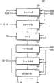
图1是示出根据本发明示例性实施例的作为一种平板显示器的实例的液晶显示器的框图;1 is a block diagram illustrating a liquid crystal display as an example of a flat panel display according to an exemplary embodiment of the present invention;
图2是详细地示出图1的显示器可以使用的数据驱动电路的实施例的框图;2 is a block diagram illustrating in detail an embodiment of a data drive circuit that the display of FIG. 1 can use;
图3是示出图1的显示器可以使用的控制电路的实施例的框图;Figure 3 is a block diagram illustrating an embodiment of a control circuit that may be used with the display of Figure 1;
图4是用于图3中所示的控制电路的信号的时序图;FIG. 4 is a timing diagram of signals for the control circuit shown in FIG. 3;
图5是示出栅极截止电压和第二行锁存信号之间的关系的视图;以及FIG. 5 is a view showing a relationship between a gate-off voltage and a second row latch signal; and
图6是示出根据本发明另一实施例的控制电路的电路图。FIG. 6 is a circuit diagram showing a control circuit according to another embodiment of the present invention.
具体实施方式Detailed ways
应当理解,当元件或层被指出“位于”、“连接到”、“耦合到”另一个元件或层上时,该元件可直接位于、连接到、或耦合到另一个元件或层上,或者也可在其间存在插入的元件或层。相反地,当元件或层被指出“直接位于”、“直接连接到”、“直接耦合到”另一个元件或层上时,是指不存在插入的元件或层。通篇中相同的标号表示相同的元件。正如在此所应用的,术语“和/或”包括任何的以及所有的一个或多个相关所列术语的结合。It will be understood that when an element or layer is referred to as being "on," "connected to," or "coupled to" another element or layer, the element can be directly on, connected to, or coupled to the other element or layer, or Intervening elements or layers may also be present. In contrast, when an element or layer is referred to as being "directly on," "directly connected to," or "directly coupled to" another element or layer, it means that there are no intervening elements or layers present. Like reference numerals refer to like elements throughout. As used herein, the term "and/or" includes any and all combinations of one or more of the associated listed items.
应当理解,尽管在此可能使用术语第一、第二等来描述不同的元件、部件、区域、层、和/或部分,但是这些元件、部件、区域、层、和/或部分并不局限于这些术语。这些术语仅用于将一个元件、部件、区域、层、或部分与另一个区域、层、或部分相区分。因此,在不背离本发明宗旨的情况下,下文所述的第一元件、组件、区域、层、或部分可以称为第二元件、组件、区域、层、或部分。被描述为“第一”的元件并不意味着需要存在“第二”或其它元件。It should be understood that although the terms first, second, etc. may be used herein to describe various elements, components, regions, layers, and/or sections, these elements, components, regions, layers, and/or sections are not limited to these terms. These terms are only used to distinguish one element, component, region, layer or section from another region, layer or section. Therefore, a first element, component, region, layer or section discussed below could be termed a second element, component, region, layer or section without departing from the spirit of the present invention. An element described as a "first" does not imply that a "second" or other element needs to be present.
为了便于说明,在此可能使用诸如“在...之下”、“在...下面”、“下面的”、“在...上面”、以及“上面的”等的空间关系术语,以描述如图中所示的一个元件或机构与另一元件或机构的关系。应当理解,除图中所示的方位之外,空间关系术语将包括使用或操作中的装置的各种不同的方位。例如,如果翻转图中所示的装置,则被描述为在其他元件或机构“下面”或“之下”的元件将被定位为在其他元件或机构的“上面”。因此,示例性术语“在...下面”包括在上面和在下面的方位。装置可以以其它方式定位(旋转90度或在其他方位),并且通过在此使用的空间关系描述符进行相应地解释。For ease of description, spatial relational terms such as "under", "beneath", "beneath", "above", and "above" may be used herein, To describe the relationship of one element or mechanism to another element or mechanism as shown in the figures. It will be understood that the spatially relative terms are intended to encompass different orientations of the device in use or operation in addition to the orientation depicted in the figures. For example, if the device in the figures is turned over, elements described as "below" or "beneath" other elements or features would then be oriented "above" the other elements or features. Thus, the exemplary term "below" encompasses an orientation of above as well as below. A device may be otherwise oriented (rotated 90 degrees or at other orientations) and interpreted accordingly by the spatially relative descriptors used herein.
此使用的术语仅用于描述特定实施例而不是限制本发明的目的。正如在此使用的,单数形式的“一个”、“这个”也包括复数形式,除非文中有其它明确指示。应当进一步理解,当在本说明书中使用术语“包括”和/或“包含”时,是指存在所声称的特征、整数、步骤、操作、元件、和/或部件,但是并不排除还存在或添加一个或多个其它的特征、整数、步骤、操作、元件、部件、和/或其组合。The terminology used herein is for the purpose of describing particular embodiments only and not for the purpose of limiting the invention. As used herein, the singular forms "a", "the" and "the" also include plural forms, unless the context clearly indicates otherwise. It should be further understood that when the terms "comprising" and/or "comprising" are used in this specification, it means that there are claimed features, integers, steps, operations, elements, and/or parts, but it does not exclude that there are also or One or more other features, integers, steps, operations, elements, parts, and/or combinations thereof are added.
除非特别限定,在此所采用的所有的术语(包括技术和科技术语)具有与本发明所属领域的普通技术人员通常所理解的意思相同的解释。而该术语的进一步理解,例如,字典中通常采用的限定意思应该被解释为与相关技术上下文中的意思相一致,并且除非在此进行特别限定,其不应被解释为理想的或者过于正式的解释。Unless otherwise defined, all terms (including technical and scientific terms) used herein have the same meaning as commonly understood by one of ordinary skill in the art to which this invention belongs. For a further understanding of the term, for example, the limited meaning usually adopted in dictionaries should be interpreted as consistent with the meaning in the relevant technical context, and unless specifically defined here, it should not be interpreted as ideal or too formal explain.
以下,将参考附图详细描述本发明的实施例。Hereinafter, embodiments of the present invention will be described in detail with reference to the accompanying drawings.
图1是根据本发明的示例性实施例的作为一种平板显示器的液晶显示器100的框图。FIG. 1 is a block diagram of a liquid crystal display 100 as a type of flat panel display according to an exemplary embodiment of the present invention.
参考图1,液晶显示器100包括定时控制器110、数据驱动电路120、直流/直流(DC/DC)转换器130、栅极驱动电路140、液晶面板150、以及控制电路160。Referring to FIG. 1 , a liquid crystal display 100 includes a timing controller 110 , a
液晶面板150包括多条栅极线G1-Gn、多条与栅极线G1-Gn交叉以形成多个像素的数据线D1-Dm、以及分别形成在多个像素区中的多个像素。像素以矩阵形状排列。每个像素均包括薄膜晶体管、液晶电容器(未示出)、以及存储电容器(未示出)。The liquid crystal panel 150 includes a plurality of gate lines G1-Gn, a plurality of data lines D1-Dm crossing the gate lines G1-Gn to form a plurality of pixels, and a plurality of pixels respectively formed in a plurality of pixel regions. Pixels are arranged in a matrix shape. Each pixel includes a thin film transistor, a liquid crystal capacitor (not shown), and a storage capacitor (not shown).
薄膜晶体管包括栅电极,电连接到栅极线;数据电极,电连接到数据线;以及漏电极,电连接到液晶电容器。当通过栅极驱动电路140顺序选择栅极线G1-Gn,并且以脉冲形状将栅极导通电压VON施加到所选择的栅极线时,连接到所选择的栅极线的薄膜晶体管被导通,并且数据驱动电路120将具有像素信息的电压(对应于所关联像素的期望图像部分的电压)施加于所关联的数据线。具有像素信息的电压通过由栅极导通电压VON导通的薄膜晶体管施加于液晶电容器和存储电容器。结果,液晶电容器和存储电容器被充电,并在液晶面板150上显示预定的图像部分。The thin film transistor includes a gate electrode electrically connected to the gate line; a data electrode electrically connected to the data line; and a drain electrode electrically connected to the liquid crystal capacitor. When the gate lines G1-Gn are sequentially selected by the gate driving circuit 140, and the gate-on voltage VON is applied to the selected gate lines in a pulse shape, the thin film transistors connected to the selected gate lines are turned on. is turned on, and the
定时控制器110接收来自外部图像源的垂直同步信号Vsync、水平同步信号Hsync、数据使能信号DE、时钟信号MCLK、和像素信号RGB。在格式化像素数据RGB之后,定时控制器110输出用于液晶面板150的像素数据信号R’、G’、B’。定时控制器110还将水平起始信号STH和时钟信号HLCK施加到数据驱动电路120,并将第一行锁存信号TP1施加到控制电路160。The timing controller 110 receives a vertical sync signal Vsync, a horizontal sync signal Hsync, a data enable signal DE, a clock signal MCLK, and a pixel signal RGB from an external image source. The timing controller 110 outputs pixel data signals R', G', B' for the liquid crystal panel 150 after formatting the pixel data RGB. The timing controller 110 also applies the horizontal start signal STH and the clock signal HLCK to the
此外,定时控制器110响应于水平同步信号Hsync、垂直同步信号Vsync以及数据使能信号DE,将垂直起始信号STV、栅极时钟信号CPV、和输出使能信号OE施加到栅极驱动电路140。In addition, the timing controller 110 applies a vertical start signal STV, a gate clock signal CPV, and an output enable signal OE to the gate driving circuit 140 in response to the horizontal synchronization signal Hsync, the vertical synchronization signal Vsync, and the data enable signal DE. .
控制电路160接收外部电源电压CVDD和来自定时控制器110的第一行锁存信号TP1,以输出第二行锁存信号TP2。The control circuit 160 receives the external power supply voltage CVDD and the first row latch signal TP1 from the timing controller 110 to output the second row latch signal TP2.
响应于第二行锁存信号TP2以及来自定时控制器110的像素数据信号R’、G’、B’、水平起始信号STH、和时钟信号HCLK,数据驱动电路120输出信号以驱动数据线D1-Dm。在一些实施例中,数据驱动电路120被设置成具有多个集成电路。In response to the second row latch signal TP2 and pixel data signals R′, G′, B′, horizontal start signal STH, and clock signal HCLK from the timing controller 110, the
栅极驱动电路140响应于从定时控制器110施加的信号,顺序地扫描液晶面板150的栅极线G1-Gn。在此,栅极驱动电路140的扫描操作意味着栅极驱动电路140顺序地将栅极导通电压施加到栅极线,使得连接到被施加有栅极导通电压的栅极线的像素处于数据可写状态。例如,对于包括液晶电容器的像素,将足够的栅极导通电压施加到与其相关的栅极线导致相关数据线电压(对应于像素的期望图像部分)和液晶电容器之间的电气通信。The gate driving circuit 140 sequentially scans the gate lines G1 -Gn of the liquid crystal panel 150 in response to signals applied from the timing controller 110 . Here, the scanning operation of the gate driving circuit 140 means that the gate driving circuit 140 sequentially applies the gate-on voltage to the gate lines so that the pixels connected to the gate lines to which the gate-on voltage is applied are at Data can be written. For example, for a pixel that includes a liquid crystal capacitor, applying a sufficient gate-on voltage to its associated gate line results in electrical communication between the associated data line voltage (corresponding to the desired image portion of the pixel) and the liquid crystal capacitor.
DC/DC转换器130响应于外部电源电压CVDD,产生用于驱动液晶显示器100的数据驱动电压DVDD和AVDD、栅极导通电压VON、栅极截止电压VOFF、以及共电极电压VCOM。The DC/DC converter 130 generates data driving voltages DVDD and AVDD, a gate-on voltage VON, a gate-off voltage VOFF, and a common electrode voltage VCOM for driving the liquid crystal display 100 in response to an external power supply voltage CVDD.
图2是详细地示出图1的数据驱动电路120的实施例的框图。FIG. 2 is a block diagram illustrating an embodiment of the
参考图2,数据驱动电路120包括移位寄存器210,产生采样信号;数据寄存器220,响应于采样信号将像素数据R’、G’、B’存储在其中;锁存器230,锁存由数据寄存器220提供的像素数据R’、G’、B’;电平移位器240,增加来自锁存器230的像素数据的幅值;数/模(D/A)转换器250,将从电平移位器240输出的像素数据转换为模拟信号;以及输出缓冲器260。Referring to FIG. 2, the
移位寄存器210响应于时钟信号HCLK,使来自定时控制器110的水平起始信号STH顺序地移位,以输出经移位的水平起始信号作为采样信号。The
数据寄存器220响应于来自移位寄存器210的采样信号,对来自定时控制器110的像素数据R’、G’、B’进行采样,并将采样的像素数据R’、G’、B’存储于此。数据寄存器220具有对应于通过将水平方向上的像素的数量与各个像素数据的位数相乘所得到的值的大小。锁存器230锁存来自数据寄存器220的像素数据R’、G’、B’,并响应于来自控制电路160的第二行锁存信号TP2,输出锁存的像素数据R’、G’、B’。The data register 220 samples the pixel data R', G', B' from the timing controller 110 in response to the sampling signal from the
电平移位器240执行电平位移运算,以增加从锁存器230输出的像素数据R’、G’、B’的电压摆动宽度(voltage swing width)。D/A转换器250将来自电平移位器240的像素数据转换为具有灰度级电压V0-V11的模拟像素数据信号。输出缓冲器260存储从D/A转换器250输出的模拟像素数据信号,并响应于液晶面板150的第二行锁存信号TP2,将具有所存储的模拟像素数据信号提供给数据线D1-Dm。例如,锁存器230在第二行锁存信号TP2的上升沿时,将来自数据寄存器220的像素数据R’、G’、B’输出到电平移位器240,并在第二行锁存信号TP2的下降沿时,输出缓冲器260将来自D/A转换器250的模拟像素数据信号提供给数据线D1-Dm。The
当在开启电源之后,开始将数据驱动电压DVDD施加到数据驱动电路120时,移位寄存器210、数据寄存器220、和锁存器230被驱动,但是在输入第二行锁存信号TP2之前,锁存器230维持在不定状态。当将来自DC/DC转换器130的数据驱动电压AVDD施加到数据驱动电路120时,将从锁存器230输出的像素数据信号通过电平移位器240、D/A转换器250和输出缓冲器260施加到数据线D1-Dm。在栅极截止电压VOFF低于足以使薄膜晶体管截止的电平之前,薄膜晶体管维持在轻微导通状态。结果,通过薄膜晶体管将施加到数据线D1-Dm的像素数据信号传送到液晶电容器,从而在液晶面板150上显示错误的图像。When the data driving voltage DVDD starts to be applied to the
为了防止在液晶面板150上显示错误的图像,在开启电源之后,至少到栅极截止电压低于足以使薄膜晶体管截止之前,电平控制电路160输出高电平的第二行锁存信号TP2,以复位锁存器230的输出。因此,数据驱动电路120可以被维持在复位状态,而第二行锁存信号TP2被维持在高电平。In order to prevent wrong images from being displayed on the liquid crystal panel 150, after the power is turned on, at least until the gate cut-off voltage is lower than enough to turn off the thin film transistor, the level control circuit 160 outputs a high-level second row latch signal TP2, to reset the output of
图3是示出图1的控制电路的框图。FIG. 3 is a block diagram illustrating a control circuit of FIG. 1 .
参考图3,控制电路160包括延迟电路310、脉冲发生器320、和逻辑电路330。延迟电路310将外部电源电压CVDD延迟预定的时间,以输出信号D_CVDD。脉冲发生器320接收信号D_CVDD和外部电源电压CVDD,并输出脉冲信号PLS。逻辑电路330接收来自定时控制器110的第一行锁存信号TP1以及来自脉冲发生器320的脉冲信号PLS,以输出第二行锁存信号TP2。在本发明的示例性实施例中,逻辑电路330可以为逻辑运算电路(其可以包括一个或多个逻辑门)。例如,逻辑电路330可以包括逻辑“或”运算电路。Referring to FIG. 3 , the control circuit 160 includes a delay circuit 310 , a pulse generator 320 , and a logic circuit 330 . The delay circuit 310 delays the external power supply voltage CVDD for a predetermined time to output the signal D_CVDD. The pulse generator 320 receives the signal D_CVDD and the external power supply voltage CVDD, and outputs a pulse signal PLS. The logic circuit 330 receives the first row latch signal TP1 from the timing controller 110 and the pulse signal PLS from the pulse generator 320 to output the second row latch signal TP2 . In an exemplary embodiment of the present invention, the logic circuit 330 may be a logic operation circuit (which may include one or more logic gates). For example, the logic circuit 330 may include a logic "OR" operation circuit.
图4是图3中所示的控制电路160的实施例的信号的时序图。图5是示出栅极截止电压VOFF和第二行锁存信号TP2之间的关系的视图。FIG. 4 is a timing diagram of signals of the embodiment of the control circuit 160 shown in FIG. 3 . FIG. 5 is a view showing the relationship between the gate-off voltage VOFF and the second row latch signal TP2.
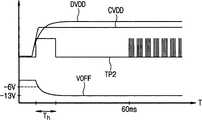
参考图4和图5,在将外部电源电压CVDD施加到液晶显示器100之后,第二行锁存信号TP2维持在高电平达预定时间Th。第二行锁存信号TP2的高电平周期Th对应于延迟电路310的延迟时间,并且基本上与在栅极截止电压VOFF低于足以使薄膜晶体管截止的电平之前所经过的时间相等。在一些实施例中,第二行锁存信号TP2的高电平周期Th大约为5毫秒或更多。Referring to FIGS. 4 and 5, after the external power supply voltage CVDD is applied to the liquid crystal display 100, the second row latch signal TP2 is maintained at a high level for a predetermined timeTh . The high level period Th of the second row latch signal TP2 corresponds to the delay time of the delay circuit 310 and is substantially equal to the time elapsed before the gate-off voltage VOFF is lower than a level sufficient to turn off the thin film transistor. In some embodiments, the high level period Th of the second row latch signal TP2 is about 5 milliseconds or more.
因为在将数据驱动电压DVDD和AVDD施加到数据驱动电路120之前,将第二行锁存信号TP2设置为高电平,所以在将数据驱动电压DVDD和AVDD施加到数据驱动电路120之前,将如图2所示的锁存器230和输出缓冲器260的输出复位。因此,数据线D1-Dm未被驱动,直到栅极截止信号低于足以使薄膜晶体管截止的电平,从而防止在开启液晶显示器100时在液晶面板150上显示错误的图像。如图4所示,在经过由延迟电路320所产生的延迟时间之后,第二行锁存信号TP2显示出与来自定时控制器110的第一行锁存信号TP1相同的波形。Since the second row latch signal TP2 is set to a high level before the data driving voltages DVDD and AVDD are applied to the
图6是示出了根据本发明另一示例性实施例的控制电路600的电路图。FIG. 6 is a circuit diagram illustrating a
参考图6,控制电路600包括延迟电路610、脉冲发生电路620、和输出电路630。延迟电路600包括连接在外部电源电压CVDD和节点613之间的第一电阻器611,并且还包括连接到节点613和接地的电容器612。节点613处的电压在图6中被称作PCVDD。脉冲发生电路620包括第二电阻器621,该第二电阻器具有施加有外部电源电压CVDD的第一端。第二电阻器621的第二端和晶体管622的第一端通过节点623连接。晶体管622的第二端接地,而晶体管622的栅极连接到节点613。Referring to FIG. 6 , the
输出电路630包括第一二极管631,该第一二极管具有连接到第二电阻器621和晶体管622之间的节点623的输入端以及从其输出第二行锁存信号TP2的输出端。节点623处的电压在图6中被称作PLS。输出电路630还包括第二二极管632,该第二二极管具有施加有第一行锁存信号TP1的输入端以及与第一二极管631的输出端和第三电阻器633共同连接的输出端。第三电阻器633连接在第一和第二二极管631和632的输出端与接地之间。从第一和第二二极管631和632的输出端输出第二行锁存信号TP2。The
以下,将详细描述图6中所示的控制单元的操作。Hereinafter, the operation of the control unit shown in FIG. 6 will be described in detail.
在将外部电源电压施加到液晶显示器100之后,外部电源电压CVDD通过第二电阻器621和第一二极管631作为第二行锁存信号TP2被输出,同时晶体管622截止。在经过由第一电阻器611的电阻和电容器612的电容决定的时间之后,晶体管622的栅极处的电压PCVDD从其初始值改变为基本上等于CVDD的电压。在预定时间(也取决于第一电阻器611的电阻和电容器612的电容)之后,当通过第一电阻器611和电容器612使晶体管622导通时,节点623处的电压PLS接近接地,并且二极管631截止。随后,通过第二二极管632的输出端输出来自定时控制器110的第一行锁存信号TP1(即,信号TP1根据其值使二极管632导通和截止)。因此,在开启电源之后,经过由第一电阻器611和电容器612所产生的预定时间(延迟时间),第二行锁存信号TP2具有与来自定时控制器110的第一行锁存信号TP1相同的波形。After the external power supply voltage is applied to the liquid crystal display 100, the external power supply voltage CVDD is output as the second row latch signal TP2 through the
根据以上描述,在开始显示器的电源导通状态时,在将数据驱动电压施加到数据驱动电路之前,控制数据驱动电路中的锁存的行锁存信号被设置为高电平。因此,虽然将数据驱动电压施加到数据驱动电路,但是锁存并没有输出数据信号。结果,因为直到经过预定时间才驱动数据线,所以液晶显示器可以防止在液晶面板上显示错误的图像,其中,预定时间约等于或大于使栅极截止电压低于足以将薄膜晶体管截止的电平的时间。According to the above description, at the start of the power-on state of the display, before the data driving voltage is applied to the data driving circuit, the row latch signal controlling the latch in the data driving circuit is set to a high level. Therefore, although the data driving voltage is applied to the data driving circuit, the latch does not output the data signal. As a result, the liquid crystal display can prevent an erroneous image from being displayed on the liquid crystal panel because the data line is not driven until a predetermined time has elapsed, wherein the predetermined time is approximately equal to or greater than a time for making the gate-off voltage lower than a level sufficient to turn off the thin film transistor. time.
尽管描述了本发明的示例性实施例,但是应该理解本发明不局限于这些示例性实施例,在由权利要求所限定的本发明的精神和范围内,本领域的技术人员可以做出各种改变和修改。Although exemplary embodiments of the present invention have been described, it should be understood that the present invention is not limited to these exemplary embodiments, and those skilled in the art can make various modifications within the spirit and scope of the present invention defined by the claims. change and modification.
Claims (18)
Applications Claiming Priority (3)
| Application Number | Priority Date | Filing Date | Title |
|---|---|---|---|
| KR1020050098210 | 2005-10-18 | ||
| KR1020050098210AKR101267019B1 (en) | 2005-10-18 | 2005-10-18 | Flat panel display |
| KR10-2005-0098210 | 2005-10-18 |
Publications (2)
| Publication Number | Publication Date |
|---|---|
| CN1953007A CN1953007A (en) | 2007-04-25 |
| CN1953007Btrue CN1953007B (en) | 2011-03-16 |
Family
ID=37947722
Family Applications (1)
| Application Number | Title | Priority Date | Filing Date |
|---|---|---|---|
| CN2006101528015AActiveCN1953007B (en) | 2005-10-18 | 2006-10-18 | Flat panel display and operation method thereof |
Country Status (5)
| Country | Link |
|---|---|
| US (1) | US20070085801A1 (en) |
| JP (1) | JP4939847B2 (en) |
| KR (1) | KR101267019B1 (en) |
| CN (1) | CN1953007B (en) |
| TW (1) | TWI420449B (en) |
Families Citing this family (43)
| Publication number | Priority date | Publication date | Assignee | Title |
|---|---|---|---|---|
| EP1825455A4 (en)* | 2004-11-16 | 2009-05-06 | Ignis Innovation Inc | System and driving method for active matrix light emitting device display |
| CA2490858A1 (en) | 2004-12-07 | 2006-06-07 | Ignis Innovation Inc. | Driving method for compensated voltage-programming of amoled displays |
| JP5355080B2 (en) | 2005-06-08 | 2013-11-27 | イグニス・イノベイション・インコーポレーテッド | Method and system for driving a light emitting device display |
| US9489891B2 (en) | 2006-01-09 | 2016-11-08 | Ignis Innovation Inc. | Method and system for driving an active matrix display circuit |
| US9269322B2 (en) | 2006-01-09 | 2016-02-23 | Ignis Innovation Inc. | Method and system for driving an active matrix display circuit |
| WO2007079572A1 (en) | 2006-01-09 | 2007-07-19 | Ignis Innovation Inc. | Method and system for driving an active matrix display circuit |
| KR101408253B1 (en)* | 2007-09-11 | 2014-07-02 | 엘지디스플레이 주식회사 | Driving circuit for a liquid crystal display and driving method thereof |
| EP2277163B1 (en)* | 2008-04-18 | 2018-11-21 | Ignis Innovation Inc. | System and driving method for light emitting device display |
| CA2637343A1 (en) | 2008-07-29 | 2010-01-29 | Ignis Innovation Inc. | Improving the display source driver |
| TWI397037B (en)* | 2008-10-28 | 2013-05-21 | Chunghwa Picture Tubes Ltd | Source driver ic for display and output control circuit thereof |
| US9370075B2 (en) | 2008-12-09 | 2016-06-14 | Ignis Innovation Inc. | System and method for fast compensation programming of pixels in a display |
| US8497828B2 (en) | 2009-11-12 | 2013-07-30 | Ignis Innovation Inc. | Sharing switch TFTS in pixel circuits |
| CA2687631A1 (en) | 2009-12-06 | 2011-06-06 | Ignis Innovation Inc | Low power driving scheme for display applications |
| KR101111529B1 (en)* | 2010-01-29 | 2012-02-15 | 주식회사 실리콘웍스 | Source driver circuit of liquid crystal display |
| CA2696778A1 (en) | 2010-03-17 | 2011-09-17 | Ignis Innovation Inc. | Lifetime, uniformity, parameter extraction methods |
| KR101407308B1 (en)* | 2010-12-14 | 2014-06-13 | 엘지디스플레이 주식회사 | Driving circuit for liquid crystal display device and method for driving the same |
| US20140368491A1 (en) | 2013-03-08 | 2014-12-18 | Ignis Innovation Inc. | Pixel circuits for amoled displays |
| US9886899B2 (en) | 2011-05-17 | 2018-02-06 | Ignis Innovation Inc. | Pixel Circuits for AMOLED displays |
| US9351368B2 (en) | 2013-03-08 | 2016-05-24 | Ignis Innovation Inc. | Pixel circuits for AMOLED displays |
| US9881587B2 (en) | 2011-05-28 | 2018-01-30 | Ignis Innovation Inc. | Systems and methods for operating pixels in a display to mitigate image flicker |
| US9747834B2 (en) | 2012-05-11 | 2017-08-29 | Ignis Innovation Inc. | Pixel circuits including feedback capacitors and reset capacitors, and display systems therefore |
| US9336717B2 (en) | 2012-12-11 | 2016-05-10 | Ignis Innovation Inc. | Pixel circuits for AMOLED displays |
| US9786223B2 (en) | 2012-12-11 | 2017-10-10 | Ignis Innovation Inc. | Pixel circuits for AMOLED displays |
| CA2894717A1 (en) | 2015-06-19 | 2016-12-19 | Ignis Innovation Inc. | Optoelectronic device characterization in array with shared sense line |
| US9721505B2 (en) | 2013-03-08 | 2017-08-01 | Ignis Innovation Inc. | Pixel circuits for AMOLED displays |
| US10442355B2 (en)* | 2014-09-17 | 2019-10-15 | Intel Corporation | Object visualization in bowl-shaped imaging systems |
| CA2873476A1 (en) | 2014-12-08 | 2016-06-08 | Ignis Innovation Inc. | Smart-pixel display architecture |
| CA2886862A1 (en) | 2015-04-01 | 2016-10-01 | Ignis Innovation Inc. | Adjusting display brightness for avoiding overheating and/or accelerated aging |
| CA2898282A1 (en) | 2015-07-24 | 2017-01-24 | Ignis Innovation Inc. | Hybrid calibration of current sources for current biased voltage progra mmed (cbvp) displays |
| US10373554B2 (en) | 2015-07-24 | 2019-08-06 | Ignis Innovation Inc. | Pixels and reference circuits and timing techniques |
| US10657895B2 (en) | 2015-07-24 | 2020-05-19 | Ignis Innovation Inc. | Pixels and reference circuits and timing techniques |
| CA2908285A1 (en) | 2015-10-14 | 2017-04-14 | Ignis Innovation Inc. | Driver with multiple color pixel structure |
| KR102498501B1 (en)* | 2015-12-31 | 2023-02-10 | 엘지디스플레이 주식회사 | Display device and driving method thereof |
| KR102609948B1 (en)* | 2016-09-30 | 2023-12-04 | 엘지디스플레이 주식회사 | Display panel driving unit, its driving method, and display device including the same |
| KR102552006B1 (en) | 2016-11-22 | 2023-07-05 | 주식회사 엘엑스세미콘 | Data driving device and display device including the same |
| KR102399178B1 (en)* | 2017-08-11 | 2022-05-19 | 삼성디스플레이 주식회사 | Data driver and display apparatus having the same |
| KR102505197B1 (en)* | 2018-07-25 | 2023-03-03 | 삼성디스플레이 주식회사 | Display device and driving method thereof |
| KR102715269B1 (en)* | 2018-08-29 | 2024-10-10 | 엘지디스플레이 주식회사 | Gate driver, organic light emitting display apparatus and driving method thereof |
| US11217144B2 (en)* | 2019-11-06 | 2022-01-04 | Silicon Works Co., Ltd. | Driver integrated circuit and display device including the same |
| CN111341242B (en)* | 2020-04-09 | 2021-09-03 | Tcl华星光电技术有限公司 | Circuit driving system, driving chip and display device |
| KR102813513B1 (en)* | 2020-12-31 | 2025-05-27 | 엘지디스플레이 주식회사 | Display device and driving method threrof |
| CN113299244B (en)* | 2021-05-24 | 2023-02-07 | 京东方科技集团股份有限公司 | Voltage control module, driving method and display device |
| KR20230095543A (en)* | 2021-12-22 | 2023-06-29 | 엘지디스플레이 주식회사 | Data Driver and Display Device including the same |
Citations (1)
| Publication number | Priority date | Publication date | Assignee | Title |
|---|---|---|---|---|
| CN1229227A (en)* | 1998-03-17 | 1999-09-22 | 明碁电脑股份有限公司 | Liquid crystal monitor with liquid crystal display panel protection circuit |
Family Cites Families (9)
| Publication number | Priority date | Publication date | Assignee | Title |
|---|---|---|---|---|
| JPS61238026A (en)* | 1985-04-15 | 1986-10-23 | Sharp Corp | Liquid crystal driving device |
| JPH01253798A (en)* | 1988-04-01 | 1989-10-11 | Matsushita Electric Ind Co Ltd | drive circuit |
| JPH04278988A (en)* | 1991-03-07 | 1992-10-05 | Fuji Electric Co Ltd | Display drive circuit for display panel |
| JPH08304773A (en)* | 1995-05-08 | 1996-11-22 | Nippondenso Co Ltd | Matrix type liquid crystal display device |
| US6529190B2 (en)* | 1998-09-30 | 2003-03-04 | Sony Corporation | Method and apparatus for monitoring/shutting down a power line within a display device |
| JP2002101316A (en)* | 2000-09-26 | 2002-04-05 | Mitsubishi Electric Corp | Clock generation circuit and image display device |
| KR100806904B1 (en) | 2001-10-30 | 2008-02-22 | 삼성전자주식회사 | Driving device of liquid crystal display |
| JP4158658B2 (en)* | 2003-09-10 | 2008-10-01 | セイコーエプソン株式会社 | Display driver and electro-optical device |
| TWM253032U (en)* | 2004-03-16 | 2004-12-11 | Niko Semiconductor Co Ltd | Push-pull control signal generation circuit |
- 2005
- 2005-10-18KRKR1020050098210Apatent/KR101267019B1/ennot_activeExpired - Lifetime
- 2006
- 2006-05-23USUS11/440,338patent/US20070085801A1/ennot_activeAbandoned
- 2006-06-13JPJP2006162971Apatent/JP4939847B2/enactiveActive
- 2006-09-11TWTW095133529Apatent/TWI420449B/enactive
- 2006-10-18CNCN2006101528015Apatent/CN1953007B/enactiveActive
Patent Citations (1)
| Publication number | Priority date | Publication date | Assignee | Title |
|---|---|---|---|---|
| CN1229227A (en)* | 1998-03-17 | 1999-09-22 | 明碁电脑股份有限公司 | Liquid crystal monitor with liquid crystal display panel protection circuit |
Also Published As
| Publication number | Publication date |
|---|---|
| KR20070042363A (en) | 2007-04-23 |
| TW200717409A (en) | 2007-05-01 |
| JP4939847B2 (en) | 2012-05-30 |
| JP2007114732A (en) | 2007-05-10 |
| US20070085801A1 (en) | 2007-04-19 |
| CN1953007A (en) | 2007-04-25 |
| KR101267019B1 (en) | 2013-05-30 |
| TWI420449B (en) | 2013-12-21 |
Similar Documents
| Publication | Publication Date | Title |
|---|---|---|
| CN1953007B (en) | Flat panel display and operation method thereof | |
| CN110262696B (en) | Gate driver circuit and touch screen integrated display device | |
| CN102968952B (en) | Scan driver and organic light emitting display device using thereof | |
| CN104751764B (en) | Display device and its driving method | |
| CN111243514B (en) | Pixel driving circuit, driving method thereof and display panel | |
| CN104751763B (en) | The method of the gating shift register of display device and initialization display device | |
| CN100442343C (en) | Liquid crystal display device having a plurality of pixel electrodes | |
| CN103503057B (en) | Scan signal line drive circuit, possess its display device and the driving method of scan signal line | |
| KR101705370B1 (en) | Light emitting control unit and display device using the same | |
| CN101226713A (en) | Display device and method for driving the device | |
| CN103578394B (en) | Gate drive circuit and display device using the gate drive circuit | |
| CN106875895A (en) | Scanner driver, display device and the method for driving display device | |
| CN102486911B (en) | Organic light emitting diode display and driving method thereof | |
| US11205389B2 (en) | Scan driver and display device having same | |
| TW201229992A (en) | Scan driver and driving method thereof | |
| US8390558B2 (en) | Liquid crystal display | |
| KR20120117120A (en) | Pulse output circuit and organic light emitting diode display device using the same | |
| CN103680377B (en) | Gate shift register and use the flat faced display of this gate shift register | |
| US20150170594A1 (en) | Data driver and display device using the same | |
| US20070159439A1 (en) | Liquid crystal display | |
| KR20070118459A (en) | Display | |
| CN115346472A (en) | Gate driver and electroluminescent display device including the gate driver | |
| CN103345905B (en) | Method of Operating an Electrophoretic Display | |
| KR101977247B1 (en) | Shift register and display device using the same | |
| KR20070074841A (en) | Liquid crystal display |
Legal Events
| Date | Code | Title | Description |
|---|---|---|---|
| C06 | Publication | ||
| PB01 | Publication | ||
| C10 | Entry into substantive examination | ||
| SE01 | Entry into force of request for substantive examination | ||
| C14 | Grant of patent or utility model | ||
| GR01 | Patent grant | ||
| ASS | Succession or assignment of patent right | Owner name:SAMSUNG DISPLAY CO., LTD. Free format text:FORMER OWNER: SAMSUNG ELECTRONICS CO., LTD. Effective date:20121219 | |
| C41 | Transfer of patent application or patent right or utility model | ||
| TR01 | Transfer of patent right | Effective date of registration:20121219 Address after:Gyeonggi Do, South Korea Patentee after:Samsung Display Co., Ltd. Address before:Gyeonggi Do, South Korea Patentee before:Samsung Electronics Co., Ltd. |