CN1950781B - Surface-emitting lasers with integrated absorbers - Google Patents
Surface-emitting lasers with integrated absorbersDownload PDFInfo
- Publication number
- CN1950781B CN1950781BCN2005800107807ACN200580010780ACN1950781BCN 1950781 BCN1950781 BCN 1950781BCN 2005800107807 ACN2005800107807 ACN 2005800107807ACN 200580010780 ACN200580010780 ACN 200580010780ACN 1950781 BCN1950781 BCN 1950781B
- Authority
- CN
- China
- Prior art keywords
- absorber
- laser
- surface emitting
- quantum dot
- emitting laser
- Prior art date
- Legal status (The legal status is an assumption and is not a legal conclusion. Google has not performed a legal analysis and makes no representation as to the accuracy of the status listed.)
- Expired - Fee Related
Links
Images


Classifications
- G—PHYSICS
- G06—COMPUTING OR CALCULATING; COUNTING
- G06F—ELECTRIC DIGITAL DATA PROCESSING
- G06F1/00—Details not covered by groups G06F3/00 - G06F13/00 and G06F21/00
- G06F1/04—Generating or distributing clock signals or signals derived directly therefrom
- G06F1/10—Distribution of clock signals, e.g. skew
- G06F1/105—Distribution of clock signals, e.g. skew in which the distribution is at least partially optical
- H—ELECTRICITY
- H01—ELECTRIC ELEMENTS
- H01S—DEVICES USING THE PROCESS OF LIGHT AMPLIFICATION BY STIMULATED EMISSION OF RADIATION [LASER] TO AMPLIFY OR GENERATE LIGHT; DEVICES USING STIMULATED EMISSION OF ELECTROMAGNETIC RADIATION IN WAVE RANGES OTHER THAN OPTICAL
- H01S3/00—Lasers, i.e. devices using stimulated emission of electromagnetic radiation in the infrared, visible or ultraviolet wave range
- H01S3/10—Controlling the intensity, frequency, phase, polarisation or direction of the emitted radiation, e.g. switching, gating, modulating or demodulating
- H01S3/11—Mode locking; Q-switching; Other giant-pulse techniques, e.g. cavity dumping
- H01S3/1106—Mode locking
- H01S3/1112—Passive mode locking
- H01S3/1115—Passive mode locking using intracavity saturable absorbers
- H—ELECTRICITY
- H01—ELECTRIC ELEMENTS
- H01S—DEVICES USING THE PROCESS OF LIGHT AMPLIFICATION BY STIMULATED EMISSION OF RADIATION [LASER] TO AMPLIFY OR GENERATE LIGHT; DEVICES USING STIMULATED EMISSION OF ELECTROMAGNETIC RADIATION IN WAVE RANGES OTHER THAN OPTICAL
- H01S5/00—Semiconductor lasers
- H01S5/04—Processes or apparatus for excitation, e.g. pumping, e.g. by electron beams
- H01S5/041—Optical pumping
- H—ELECTRICITY
- H01—ELECTRIC ELEMENTS
- H01S—DEVICES USING THE PROCESS OF LIGHT AMPLIFICATION BY STIMULATED EMISSION OF RADIATION [LASER] TO AMPLIFY OR GENERATE LIGHT; DEVICES USING STIMULATED EMISSION OF ELECTROMAGNETIC RADIATION IN WAVE RANGES OTHER THAN OPTICAL
- H01S5/00—Semiconductor lasers
- H01S5/10—Construction or shape of the optical resonator, e.g. extended or external cavity, coupled cavities, bent-guide, varying width, thickness or composition of the active region
- H01S5/14—External cavity lasers
- H01S5/141—External cavity lasers using a wavelength selective device, e.g. a grating or etalon
- H—ELECTRICITY
- H01—ELECTRIC ELEMENTS
- H01S—DEVICES USING THE PROCESS OF LIGHT AMPLIFICATION BY STIMULATED EMISSION OF RADIATION [LASER] TO AMPLIFY OR GENERATE LIGHT; DEVICES USING STIMULATED EMISSION OF ELECTROMAGNETIC RADIATION IN WAVE RANGES OTHER THAN OPTICAL
- H01S5/00—Semiconductor lasers
- H01S5/10—Construction or shape of the optical resonator, e.g. extended or external cavity, coupled cavities, bent-guide, varying width, thickness or composition of the active region
- H01S5/18—Surface-emitting [SE] lasers, e.g. having both horizontal and vertical cavities
- H01S5/183—Surface-emitting [SE] lasers, e.g. having both horizontal and vertical cavities having only vertical cavities, e.g. vertical cavity surface-emitting lasers [VCSEL]
- H01S5/18302—Surface-emitting [SE] lasers, e.g. having both horizontal and vertical cavities having only vertical cavities, e.g. vertical cavity surface-emitting lasers [VCSEL] comprising an integrated optical modulator
- H—ELECTRICITY
- H01—ELECTRIC ELEMENTS
- H01S—DEVICES USING THE PROCESS OF LIGHT AMPLIFICATION BY STIMULATED EMISSION OF RADIATION [LASER] TO AMPLIFY OR GENERATE LIGHT; DEVICES USING STIMULATED EMISSION OF ELECTROMAGNETIC RADIATION IN WAVE RANGES OTHER THAN OPTICAL
- H01S5/00—Semiconductor lasers
- H01S5/40—Arrangement of two or more semiconductor lasers, not provided for in groups H01S5/02 - H01S5/30
- H01S5/42—Arrays of surface emitting lasers
- H01S5/423—Arrays of surface emitting lasers having a vertical cavity
- H—ELECTRICITY
- H01—ELECTRIC ELEMENTS
- H01S—DEVICES USING THE PROCESS OF LIGHT AMPLIFICATION BY STIMULATED EMISSION OF RADIATION [LASER] TO AMPLIFY OR GENERATE LIGHT; DEVICES USING STIMULATED EMISSION OF ELECTROMAGNETIC RADIATION IN WAVE RANGES OTHER THAN OPTICAL
- H01S3/00—Lasers, i.e. devices using stimulated emission of electromagnetic radiation in the infrared, visible or ultraviolet wave range
- H01S3/005—Optical devices external to the laser cavity, specially adapted for lasers, e.g. for homogenisation of the beam or for manipulating laser pulses, e.g. pulse shaping
- H01S3/0092—Nonlinear frequency conversion, e.g. second harmonic generation [SHG] or sum- or difference-frequency generation outside the laser cavity
- H—ELECTRICITY
- H01—ELECTRIC ELEMENTS
- H01S—DEVICES USING THE PROCESS OF LIGHT AMPLIFICATION BY STIMULATED EMISSION OF RADIATION [LASER] TO AMPLIFY OR GENERATE LIGHT; DEVICES USING STIMULATED EMISSION OF ELECTROMAGNETIC RADIATION IN WAVE RANGES OTHER THAN OPTICAL
- H01S3/00—Lasers, i.e. devices using stimulated emission of electromagnetic radiation in the infrared, visible or ultraviolet wave range
- H01S3/05—Construction or shape of optical resonators; Accommodation of active medium therein; Shape of active medium
- H01S3/06—Construction or shape of active medium
- H01S3/0602—Crystal lasers or glass lasers
- H01S3/0604—Crystal lasers or glass lasers in the form of a plate or disc
- H—ELECTRICITY
- H01—ELECTRIC ELEMENTS
- H01S—DEVICES USING THE PROCESS OF LIGHT AMPLIFICATION BY STIMULATED EMISSION OF RADIATION [LASER] TO AMPLIFY OR GENERATE LIGHT; DEVICES USING STIMULATED EMISSION OF ELECTROMAGNETIC RADIATION IN WAVE RANGES OTHER THAN OPTICAL
- H01S3/00—Lasers, i.e. devices using stimulated emission of electromagnetic radiation in the infrared, visible or ultraviolet wave range
- H01S3/05—Construction or shape of optical resonators; Accommodation of active medium therein; Shape of active medium
- H01S3/06—Construction or shape of active medium
- H01S3/0602—Crystal lasers or glass lasers
- H01S3/0615—Shape of end-face
- H—ELECTRICITY
- H01—ELECTRIC ELEMENTS
- H01S—DEVICES USING THE PROCESS OF LIGHT AMPLIFICATION BY STIMULATED EMISSION OF RADIATION [LASER] TO AMPLIFY OR GENERATE LIGHT; DEVICES USING STIMULATED EMISSION OF ELECTROMAGNETIC RADIATION IN WAVE RANGES OTHER THAN OPTICAL
- H01S3/00—Lasers, i.e. devices using stimulated emission of electromagnetic radiation in the infrared, visible or ultraviolet wave range
- H01S3/05—Construction or shape of optical resonators; Accommodation of active medium therein; Shape of active medium
- H01S3/06—Construction or shape of active medium
- H01S3/0627—Construction or shape of active medium the resonator being monolithic, e.g. microlaser
- H—ELECTRICITY
- H01—ELECTRIC ELEMENTS
- H01S—DEVICES USING THE PROCESS OF LIGHT AMPLIFICATION BY STIMULATED EMISSION OF RADIATION [LASER] TO AMPLIFY OR GENERATE LIGHT; DEVICES USING STIMULATED EMISSION OF ELECTROMAGNETIC RADIATION IN WAVE RANGES OTHER THAN OPTICAL
- H01S3/00—Lasers, i.e. devices using stimulated emission of electromagnetic radiation in the infrared, visible or ultraviolet wave range
- H01S3/09—Processes or apparatus for excitation, e.g. pumping
- H01S3/091—Processes or apparatus for excitation, e.g. pumping using optical pumping
- H01S3/094—Processes or apparatus for excitation, e.g. pumping using optical pumping by coherent light
- H01S3/094084—Processes or apparatus for excitation, e.g. pumping using optical pumping by coherent light with pump light recycling, i.e. with reinjection of the unused pump light, e.g. by reflectors or circulators
- H—ELECTRICITY
- H01—ELECTRIC ELEMENTS
- H01S—DEVICES USING THE PROCESS OF LIGHT AMPLIFICATION BY STIMULATED EMISSION OF RADIATION [LASER] TO AMPLIFY OR GENERATE LIGHT; DEVICES USING STIMULATED EMISSION OF ELECTROMAGNETIC RADIATION IN WAVE RANGES OTHER THAN OPTICAL
- H01S3/00—Lasers, i.e. devices using stimulated emission of electromagnetic radiation in the infrared, visible or ultraviolet wave range
- H01S3/10—Controlling the intensity, frequency, phase, polarisation or direction of the emitted radiation, e.g. switching, gating, modulating or demodulating
- H01S3/11—Mode locking; Q-switching; Other giant-pulse techniques, e.g. cavity dumping
- H01S3/1106—Mode locking
- H01S3/1112—Passive mode locking
- H01S3/1115—Passive mode locking using intracavity saturable absorbers
- H01S3/1118—Semiconductor saturable absorbers, e.g. semiconductor saturable absorber mirrors [SESAMs]; Solid-state saturable absorbers, e.g. carbon nanotube [CNT] based
- H—ELECTRICITY
- H01—ELECTRIC ELEMENTS
- H01S—DEVICES USING THE PROCESS OF LIGHT AMPLIFICATION BY STIMULATED EMISSION OF RADIATION [LASER] TO AMPLIFY OR GENERATE LIGHT; DEVICES USING STIMULATED EMISSION OF ELECTROMAGNETIC RADIATION IN WAVE RANGES OTHER THAN OPTICAL
- H01S5/00—Semiconductor lasers
- H01S5/02—Structural details or components not essential to laser action
- H01S5/024—Arrangements for thermal management
- H—ELECTRICITY
- H01—ELECTRIC ELEMENTS
- H01S—DEVICES USING THE PROCESS OF LIGHT AMPLIFICATION BY STIMULATED EMISSION OF RADIATION [LASER] TO AMPLIFY OR GENERATE LIGHT; DEVICES USING STIMULATED EMISSION OF ELECTROMAGNETIC RADIATION IN WAVE RANGES OTHER THAN OPTICAL
- H01S5/00—Semiconductor lasers
- H01S5/06—Arrangements for controlling the laser output parameters, e.g. by operating on the active medium
- H01S5/0607—Arrangements for controlling the laser output parameters, e.g. by operating on the active medium by varying physical parameters other than the potential of the electrodes, e.g. by an electric or magnetic field, mechanical deformation, pressure, light, temperature
- H01S5/0608—Arrangements for controlling the laser output parameters, e.g. by operating on the active medium by varying physical parameters other than the potential of the electrodes, e.g. by an electric or magnetic field, mechanical deformation, pressure, light, temperature controlled by light, e.g. optical switch
- H01S5/0609—Arrangements for controlling the laser output parameters, e.g. by operating on the active medium by varying physical parameters other than the potential of the electrodes, e.g. by an electric or magnetic field, mechanical deformation, pressure, light, temperature controlled by light, e.g. optical switch acting on an absorbing region, e.g. wavelength convertors
- H—ELECTRICITY
- H01—ELECTRIC ELEMENTS
- H01S—DEVICES USING THE PROCESS OF LIGHT AMPLIFICATION BY STIMULATED EMISSION OF RADIATION [LASER] TO AMPLIFY OR GENERATE LIGHT; DEVICES USING STIMULATED EMISSION OF ELECTROMAGNETIC RADIATION IN WAVE RANGES OTHER THAN OPTICAL
- H01S5/00—Semiconductor lasers
- H01S5/06—Arrangements for controlling the laser output parameters, e.g. by operating on the active medium
- H01S5/065—Mode locking; Mode suppression; Mode selection ; Self pulsating
- H01S5/0657—Mode locking, i.e. generation of pulses at a frequency corresponding to a roundtrip in the cavity
- H—ELECTRICITY
- H01—ELECTRIC ELEMENTS
- H01S—DEVICES USING THE PROCESS OF LIGHT AMPLIFICATION BY STIMULATED EMISSION OF RADIATION [LASER] TO AMPLIFY OR GENERATE LIGHT; DEVICES USING STIMULATED EMISSION OF ELECTROMAGNETIC RADIATION IN WAVE RANGES OTHER THAN OPTICAL
- H01S5/00—Semiconductor lasers
- H01S5/10—Construction or shape of the optical resonator, e.g. extended or external cavity, coupled cavities, bent-guide, varying width, thickness or composition of the active region
- H01S5/18—Surface-emitting [SE] lasers, e.g. having both horizontal and vertical cavities
- H01S5/183—Surface-emitting [SE] lasers, e.g. having both horizontal and vertical cavities having only vertical cavities, e.g. vertical cavity surface-emitting lasers [VCSEL]
- H01S5/18308—Surface-emitting [SE] lasers, e.g. having both horizontal and vertical cavities having only vertical cavities, e.g. vertical cavity surface-emitting lasers [VCSEL] having a special structure for lateral current or light confinement
- H—ELECTRICITY
- H01—ELECTRIC ELEMENTS
- H01S—DEVICES USING THE PROCESS OF LIGHT AMPLIFICATION BY STIMULATED EMISSION OF RADIATION [LASER] TO AMPLIFY OR GENERATE LIGHT; DEVICES USING STIMULATED EMISSION OF ELECTROMAGNETIC RADIATION IN WAVE RANGES OTHER THAN OPTICAL
- H01S5/00—Semiconductor lasers
- H01S5/10—Construction or shape of the optical resonator, e.g. extended or external cavity, coupled cavities, bent-guide, varying width, thickness or composition of the active region
- H01S5/18—Surface-emitting [SE] lasers, e.g. having both horizontal and vertical cavities
- H01S5/183—Surface-emitting [SE] lasers, e.g. having both horizontal and vertical cavities having only vertical cavities, e.g. vertical cavity surface-emitting lasers [VCSEL]
- H01S5/18341—Intra-cavity contacts
- H—ELECTRICITY
- H01—ELECTRIC ELEMENTS
- H01S—DEVICES USING THE PROCESS OF LIGHT AMPLIFICATION BY STIMULATED EMISSION OF RADIATION [LASER] TO AMPLIFY OR GENERATE LIGHT; DEVICES USING STIMULATED EMISSION OF ELECTROMAGNETIC RADIATION IN WAVE RANGES OTHER THAN OPTICAL
- H01S5/00—Semiconductor lasers
- H01S5/10—Construction or shape of the optical resonator, e.g. extended or external cavity, coupled cavities, bent-guide, varying width, thickness or composition of the active region
- H01S5/18—Surface-emitting [SE] lasers, e.g. having both horizontal and vertical cavities
- H01S5/183—Surface-emitting [SE] lasers, e.g. having both horizontal and vertical cavities having only vertical cavities, e.g. vertical cavity surface-emitting lasers [VCSEL]
- H01S5/18358—Surface-emitting [SE] lasers, e.g. having both horizontal and vertical cavities having only vertical cavities, e.g. vertical cavity surface-emitting lasers [VCSEL] containing spacer layers to adjust the phase of the light wave in the cavity
- H—ELECTRICITY
- H01—ELECTRIC ELEMENTS
- H01S—DEVICES USING THE PROCESS OF LIGHT AMPLIFICATION BY STIMULATED EMISSION OF RADIATION [LASER] TO AMPLIFY OR GENERATE LIGHT; DEVICES USING STIMULATED EMISSION OF ELECTROMAGNETIC RADIATION IN WAVE RANGES OTHER THAN OPTICAL
- H01S5/00—Semiconductor lasers
- H01S5/10—Construction or shape of the optical resonator, e.g. extended or external cavity, coupled cavities, bent-guide, varying width, thickness or composition of the active region
- H01S5/18—Surface-emitting [SE] lasers, e.g. having both horizontal and vertical cavities
- H01S5/183—Surface-emitting [SE] lasers, e.g. having both horizontal and vertical cavities having only vertical cavities, e.g. vertical cavity surface-emitting lasers [VCSEL]
- H01S5/18386—Details of the emission surface for influencing the near- or far-field, e.g. a grating on the surface
- H01S5/18388—Lenses
Landscapes
- Physics & Mathematics (AREA)
- Electromagnetism (AREA)
- Optics & Photonics (AREA)
- General Physics & Mathematics (AREA)
- Condensed Matter Physics & Semiconductors (AREA)
- Engineering & Computer Science (AREA)
- Theoretical Computer Science (AREA)
- Plasma & Fusion (AREA)
- General Engineering & Computer Science (AREA)
- Lasers (AREA)
- Semiconductor Lasers (AREA)
Abstract
Description
Translated fromChinese背景background
发明领域field of invention
本发明的领域一般而言涉及激光器,更具体但不排他地涉及一种具有集成吸收器的表面发射激光器。The field of the invention relates generally to lasers and more particularly but not exclusively to a surface emitting laser with an integrated absorber.
背景信息Background Information
半导体激光器具有包括通信系统和消费电子产品的多种应用。通常,半导体激光器可分为边缘发射激光器或表面发射激光器(SEL)。边缘发射激光器平行于半导体晶片表面发出辐射,而SEL垂直于半导体晶片表面发出辐射。半导体激光器的增益区可通过光泵浦或电泵浦来激发。Semiconductor lasers have a variety of applications including communication systems and consumer electronics. Generally, semiconductor lasers can be classified as edge-emitting lasers or surface-emitting lasers (SELs). Edge-emitting lasers emit radiation parallel to the semiconductor wafer surface, while SELs emit radiation perpendicular to the semiconductor wafer surface. The gain region of a semiconductor laser can be excited by optical or electrical pumping.
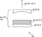
SEL的两种常见类型是垂直腔表面发射激光器(VCSEL)和垂直外腔表面发射激光器(VECSEL)。参考图1A,示出了VCSEL 100。增益区106夹在镜面(mirror)104和镜面108之间。这种镜面包括分布布拉格反射器(DBR)镜面。镜面104和镜面108限定了激光腔112。激光输出110垂直于增益区106从镜面108发射。Two common types of SELs are vertical cavity surface emitting lasers (VCSELs) and vertical external cavity surface emitting lasers (VECSELs). Referring to FIG. 1A , a VCSEL 100 is shown. Gain region 106 is sandwiched between mirror 104 and mirror 108 . Such mirrors include distributed Bragg reflector (DBR) mirrors. Mirror 104 and mirror 108 define laser cavity 112 . Laser output 110 is emitted from mirror 108 perpendicular to gain region 106 .
图1B示出VECSEL 150。镜面158安装在外部并且放置在增益区156上方。镜面154和158限定了激光腔162。镜面154包括DBR镜面。激光输出160从镜面158发射。1B shows VECSEL 150. A mirror 158 is mounted externally and placed above the gain region 156 . Mirrors 154 and 158 define
锁模激光器被用于以皮秒或更小的时间尺度产生狭窄光脉冲。通常,锁模包括对准激光纵模的相位,从而导致在激光输出中短脉冲的周期序列。图1C示出锁模激光器的光功率与时间的关系的曲线图165。激光输出的重复率基于在曲线图165中脉冲之间的周期。锁模可通过主动锁模或被动锁模来实现。主动锁模通过外部受控的调制器来使用频率调制或振幅调制。被动锁模通过可包括可饱和吸收器材料的吸收器来实现。可饱和吸收器材料可由半导体材料制造。可饱和吸收器材料可被固定于可包括DBR镜面的镜面,以形成半导体可饱和吸收镜(SESAM)。Mode-locked lasers are used to generate narrow pulses of light on picosecond or smaller timescales. Typically, mode locking involves aligning the phase of the longitudinal modes of the laser, resulting in a periodic sequence of short pulses in the laser output. Figure 1C shows a graph 165 of optical power versus time for a mode-locked laser. The repetition rate of the laser output is based on the period between pulses in graph 165 . Mode locking can be achieved by active mode locking or passive mode locking. Active mode locking uses frequency modulation or amplitude modulation with an externally controlled modulator. Passive mode locking is achieved by absorbers that may include saturable absorber materials. Saturable absorber materials can be fabricated from semiconductor materials. A saturable absorber material can be fixed to a mirror, which can include a DBR mirror, to form a semiconductor saturable absorber mirror (SESAM).
在被动锁模激光器中,期望的短脉冲激光输出经由吸收器提供。在激光腔中可饱和吸收器的效果是比起具有较低强度的循环辐射的部分来支持具有较高强度的循环辐射的部分。在多次往返后,这往往导致在腔中循环的单个短脉冲的形成。这种机制被称作锁模,因为在频域中它对应于在腔的纵模之间的固定相位关系的产生。在激光腔中的循环脉冲每当撞击输出耦合器时就产生一个输出脉冲。由此产生规则的脉冲序列。In passively mode-locked lasers, the desired short-pulse laser output is provided via an absorber. The effect of the saturable absorber in the laser cavity is to favor the portion of the circulating radiation with a higher intensity than the portion of the circulating radiation with a lower intensity. After many round trips, this often results in the formation of a single short pulse that circulates in the cavity. This mechanism is called mode locking, since in the frequency domain it corresponds to the generation of a fixed phase relationship between the longitudinal modes of the cavity. A cyclic pulse in the laser cavity produces an output pulse each time it hits the output coupler. This results in a regular pulse train.
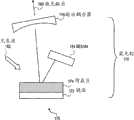
图1D示出具有非集成吸收器的VECSEL 170。VECSEL 170包括在镜面172上成层的增益区174。输出耦合器176放置在增益区174上方。镜面172和输出耦合器176限定了激光腔178。光泵浦182提供用于VECSEL 170的泵浦能量。半导体可饱和吸收镜(SESAM)184提供VECSEL 170的被动锁模,并且与增益区174分离。Figure ID shows a
目前的被动锁模激光器使用通常显示出非常相似的饱和特性的增益区和吸收器材料,以使对锁模而言在增益介质和可饱和吸收器上需要相当不同的模区域。当前在单片结构中这是无法实现的。Current passively mode-locked lasers use gain region and absorber materials that typically exhibit very similar saturation characteristics, so that considerably different mode regions are required on the gain medium and saturable absorber for mode locking. This is currently not achievable in a monolithic architecture.
附图简述Brief description of the drawings
参考下面的附图描述本发明的非限制和非穷举的实施例,其中遍及各种视图的类似的参考数字是指类似的部分,除非另有说明。Non-limiting and non-exhaustive embodiments of the present invention are described with reference to the following drawings, wherein like reference numerals refer to like parts throughout the various views, unless otherwise indicated.
图1A是说明现有技术的VCSEL的结构图。FIG. 1A is a structural diagram illustrating a prior art VCSEL.
图1B是说明现有技术的VECSEL的结构图。FIG. 1B is a structural diagram illustrating a prior art VECSEL.
图1C是说明现有技术的锁模激光器的输出脉冲的曲线图。Figure 1C is a graph illustrating the output pulses of a prior art mode-locked laser.
图1D是说明具有非集成吸收器的现有技术的VECSEL的结构图。Figure ID is a block diagram illustrating a prior art VECSEL with a non-integrated absorber.
图2A是说明根据本发明教导的具有集成吸收器的SEL的一个实施例的结构图。2A is a block diagram illustrating one embodiment of an SEL with an integrated absorber in accordance with the teachings of the present invention.
图2B是说明根据本发明教导的具有集成吸收器的SEL的一个实施例的结构图。2B is a block diagram illustrating one embodiment of an SEL with an integrated absorber in accordance with the teachings of the present invention.
图2C是根据本发明教导的具有集成吸收器的SEL的一个实施例的相对于场强的吸收器和增益层的曲线图。2C is a graph of absorber and gain layer versus field strength for one embodiment of a SEL with an integrated absorber according to the teachings of the present invention.
图2D是根据本发明教导的具有集成吸收器的SEL的一个实施例的通量(fluence)的曲线图。2D is a graph of fluence for one embodiment of a SEL with an integrated absorber according to the teachings of the present invention.
图2E是说明根据本发明教导的集成吸收器的量子点层的一个实施例的结构图。Figure 2E is a structural diagram illustrating one embodiment of a quantum dot layer of an integrated absorber according to the teachings of the present invention.
图2F是说明根据本发明教导的具有集成吸收器的SEL的一个实施例的结构图。Figure 2F is a block diagram illustrating one embodiment of an SEL with an integrated absorber in accordance with the teachings of the present invention.
图2G是说明根据本发明教导的量子阱的一个实施例的结构图。Figure 2G is a block diagram illustrating one embodiment of a quantum well in accordance with the teachings of the present invention.
图3是说明根据本发明教导的具有集成吸收器的SEL的一个实施例的结构图。Figure 3 is a block diagram illustrating one embodiment of an SEL with an integrated absorber in accordance with the teachings of the present invention.
图4是说明根据本发明教导的具有集成吸收器的SEL的一个实施例的结构图。4 is a block diagram illustrating one embodiment of an SEL with an integrated absorber in accordance with the teachings of the present invention.
图5是说明根据本发明教导的具有集成吸收器的SEL的一个实施例的结构图。5 is a block diagram illustrating one embodiment of an SEL with an integrated absorber in accordance with the teachings of the present invention.
图6是说明根据本发明教导的具有集成吸收器的SEL的一个实施例的结构图。FIG. 6 is a block diagram illustrating one embodiment of an SEL with an integrated absorber in accordance with the teachings of the present invention.
图7是说明根据本发明教导的具有集成吸收器的SEL的一个实施例的结构图。7 is a block diagram illustrating one embodiment of an SEL with an integrated absorber in accordance with the teachings of the present invention.
图8是说明根据本发明教导的具有集成吸收器的SEL的一个实施例的结构图。8 is a block diagram illustrating one embodiment of an SEL with an integrated absorber in accordance with the teachings of the present invention.
图9A是说明根据本发明教导的具有集成吸收器的SEL阵列的一个实施例的结构图。9A is a block diagram illustrating one embodiment of an SEL array with integrated absorbers in accordance with the teachings of the present invention.
图9B是说明根据本发明教导的具有集成吸收器的SEL阵列的一个实施例的透视图。9B is a perspective view illustrating one embodiment of a SEL array with integrated absorbers in accordance with the teachings of the present invention.
图10是说明根据本发明教导的通信系统的一个实施例的框图。Figure 10 is a block diagram illustrating one embodiment of a communication system according to the teachings of the present invention.
图11是说明根据本发明教导的计算机系统的一个实施例的框图。Figure 11 is a block diagram illustrating one embodiment of a computer system according to the teachings of the present invention.
图12是说明根据本发明教导的具有量子点可饱和吸收镜的固态激光器的一个实施例的结构图。Figure 12 is a block diagram illustrating one embodiment of a solid state laser with a quantum dot saturable absorber mirror in accordance with the teachings of the present invention.
图13是说明根据本发明教导的具有量子点可饱和吸收镜的固态激光器的一个实施例的结构图。Figure 13 is a block diagram illustrating one embodiment of a solid state laser with a quantum dot saturable absorber mirror in accordance with the teachings of the present invention.
详细描述A detailed description
此处描述具有集成吸收器的表面发射激光器的实施例。在下面的描述中,阐明许多特定细节以提供对本发明实施例的彻底理解。然而在相关领域的技术人员将认识到,在没有一个或多个所述特定细节的情况下,或者利用其它的方法、部件、材料等,本发明的实施例也可以得到实施。在其它情况下,未详细示出或描述众所周知的结构、材料或操作,以避免模糊本发明的多个方面。Embodiments of surface emitting lasers with integrated absorbers are described herein. In the following description, numerous specific details are set forth in order to provide a thorough understanding of embodiments of the invention. One skilled in the relevant art will recognize, however, that embodiments of the invention may be practiced without one or more of these specific details, or with other methods, components, materials, etc. In other instances, well-known structures, materials, or operations are not shown or described in detail to avoid obscuring aspects of the invention.
在整个说明书中提到的“一个实施例”或“实施例”是指结合该实施例描述的特定的特征、结构或特性被包括在本发明的至少一个实施例中。因此,在整个说明书的不同地方出现的短语“在一个实施例中”或“在实施例中”未必是指相同的实施例。此外,特定的特征、结构或特性可以以任何合适的方式被结合在一个或多个实施例中。Reference throughout this specification to "one embodiment" or "an embodiment" means that a particular feature, structure, or characteristic described in connection with the embodiment is included in at least one embodiment of the present invention. Thus, appearances of the phrases "in one embodiment" or "in an embodiment" in various places throughout the specification are not necessarily referring to the same embodiment. Furthermore, the particular features, structures or characteristics may be combined in any suitable manner in one or more embodiments.
本发明的实施例提供具有集成有增益区的吸收器的SEL。SEL的实施例提供具有高重复率(数十到数百吉赫)、高的光学平均输出功率(在电泵浦或光泵浦时数十到数百毫瓦)以及良好的光束质量(M2低于2)的超短脉冲(几十皮秒或更少)。与边缘发射半导体激光器对比,在此描述的实施例允许与锁模所需的高光束质量结合的高功率输出的可自由伸缩的模点尺寸。Embodiments of the invention provide a SEL with an absorber integrated with a gain region. Embodiments of the SEL offer high repetition rates (tens to hundreds of gigahertz), high optical average output power (tens to hundreds of milliwatts when electrically or optically pumped), and good beam quality (M2 Ultrashort pulses (tens of picoseconds or less) lower than 2). In contrast to edge emitting semiconductor lasers, the embodiments described herein allow freely scalable mode spot size for high power output combined with high beam quality required for mode locking.
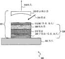
图2A说明SEL 200的一个实施例。图2A的实施例示出具有集成吸收器的光泵浦增益结构,其中吸收器放置在增益区和泵浦镜面之下。吸收器206放置在下镜面204上。下镜面204可包括半导体布拉格堆栈(stack)。下镜面204对于激光是高反射的(HR)。泵浦镜面208放置在吸收器206上。泵浦镜面208对于泵浦是高反射的,以及对于激光是部分反射的。增益区210放置在泵浦镜面208上。抗反射(AR)层212放置在增益区210上。AR层212对于激光和泵浦能量是抗反射的。下镜面204、吸收器206、泵浦镜面208、增益区210和AR层212形成单片增益结构224。在一个实施例中,单片增益结构224在单个制造过程(下面进一步讨论)中从衬底中制造。FIG. 2A illustrates one embodiment of the
输出耦合器216放置在AR层212的上方。输出耦合器216和下镜面204限定了激光腔220。在一个实施例中,输出耦合器216包括曲面输出镜面。在操作中,对SEL 200施加光泵浦214。被动锁模激光输出218从输出耦合器216发射。Output coupler 216 is placed above AR layer 212 . Output coupler 216 and lower mirror 204 define
吸收器206与增益区210集成。吸收器206包括与下镜面204、泵浦镜面208和增益区210的制造过程相适合的半导体材料。吸收器与增益区在同一半导体晶片中集成。为了把吸收器和增益区放置在同一单片结构中,吸收器和增益区应该以类似的模点尺寸操作。为了允许在增益区210和吸收器206中以类似的模尺寸的锁模,吸收器206的饱和通量必须比增益区210的饱和通量小。换言之,在达到饱和之前,增益区可比吸收器处理大得多的功率密度。将会理解,集成通常将导致在增益区和吸收器内部非常类似的模尺寸,因为增益区和吸收器在高斯激光模的瑞利范围内。激光模由下部高反射器(图2中的下镜面204)和输出耦合器(图2中的216)来限定。Absorber 206 is integrated with gain region 210 . Absorber 206 comprises a semiconductor material compatible with the fabrication process of lower mirror 204 , pump mirror 208 and gain region 210 . The absorber is integrated with the gain region in the same semiconductor die. In order to place the absorber and gain region in the same monolithic structure, the absorber and gain region should operate with similar mode spot sizes. To allow mode locking with similar mode sizes in the gain region 210 and the absorber 206 , the saturation flux of the absorber 206 must be smaller than that of the gain region 210 . In other words, the gain region can handle much greater power densities than the absorber before saturation is reached. It will be appreciated that integration will generally result in very similar mode sizes inside the gain region and absorber since the gain region and absorber are within the Rayleigh range of the Gaussian laser mode. The laser mode is defined by the lower high reflector (lower mirror 204 in Figure 2) and the output coupler (216 in Figure 2).
通量描述了在激光腔中每单位面积的光能量。当波通过诸如吸收器或增益区之类的介质时,波的一些功率由于在介质中的吸收而丧失。在吸收与通量的关系曲线中(例如图2D),吸收最初线性依赖于入射通量。当介质达到饱和通量时,曲线从线性形式断开,并且开始变平。Flux describes the light energy per unit area in a laser cavity. When a wave passes through a medium such as an absorber or gain region, some of the wave's power is lost due to absorption in the medium. In absorption vs. flux curves (eg, FIG. 2D ), absorption initially depends linearly on the incident flux. When the medium reaches saturation flux, the curve breaks from its linear form and begins to flatten.
通常,半导体激光器拥有小的增益饱和通量。这对尤其是以结合高的平均激光输出功率的高重复率的被动锁模是重要的。如果增益材料的饱和能量太高,那么可能出现调Q不稳定性,如果需要高重复率,特别是如果同时需要高的激光输出功率,那么该调Q不稳定性是难于抑制的。当半导体激光器具有小的增益饱和能量时,半导体激光器不被这样的调Q不稳定性所限制。Typically, semiconductor lasers have a small gain saturation fluence. This is important especially for passive mode-locking at high repetition rates combined with high average laser output power. If the saturation energy of the gain material is too high, then Q-switching instabilities may arise, which are difficult to suppress if high repetition rates are required, especially if high laser output powers are simultaneously required. Semiconductor lasers are not limited by such Q-switching instabilities when they have small gain saturation energies.
超过几个吉赫(GHz)的重复率需要非常短的激光腔。当对于增益结构和吸收器使用分离设备时,几何约束可能限制可实现的重复率。当在增益结构和吸收器上需要大大不同的模区域时,这种限制变得甚至更严重。Repetition rates in excess of a few gigahertz (GHz) require very short laser cavities. When using separate devices for the gain structure and absorber, geometrical constraints may limit the achievable repetition rate. This limitation becomes even more severe when substantially different mode areas are required on the gain structure and absorber.
在此描述的实施例利用了具有集成吸收器的增益结构。这种结构允许非常短的线性激光腔的简单构造。折叠式镜面是不需要的。使用集成吸收器有效地消除了对于脉冲重复率的几何约束。Embodiments described herein utilize gain structures with integrated absorbers. This structure allows simple construction of very short linear laser cavities. Folding mirrors are not required. The use of an integrated absorber effectively removes the geometric constraints on the pulse repetition rate.
此外,具有减少的饱和通量的集成吸收器允许以高重复率的较高锁模输出功率。如果在吸收器上的模尺寸必须非常小以实现足够的饱和,那么热损害吸收器的危险随着增大功率和重复率而快速上升。当吸收器由显示出较小饱和通量的不同材料制成时,模尺寸可保持很大并且避免热损害,从而允许较高的输出功率和重复率。Furthermore, an integrated absorber with reduced saturation flux allows higher mode-locked output power at high repetition rates. If the mode size on the absorber must be very small to achieve sufficient saturation, the risk of thermal damage to the absorber rises rapidly with increasing power and repetition rate. When the absorber is made of a different material that exhibits a smaller saturation flux, the mode size can be kept large and thermal damage avoided, allowing higher output power and repetition rate.
而且,将吸收器集成到增益结构中可导致低的相位噪声。这可由于紧凑和稳定的装配而导致非常小的定时抖动。Also, integrating the absorber into the gain structure results in low phase noise. This can result in very little timing jitter due to the compact and stable assembly.
对于高重复率而言,吸收器介质的恢复时间通过本领域已知的适合装置来减少。这样的方法包括低温生长或离子轰击。这引入了非辐射复合中心,该中心允许由吸收产生的载波的快速捕获和复合。For high repetition rates, the recovery time of the absorber medium is reduced by suitable means known in the art. Such methods include low temperature growth or ion bombardment. This introduces a non-radiative recombination center that allows fast acquisition and recombination of the carrier produced by absorption.
在此给出减少集成吸收器的饱和通量的各种实施例。在一个实施例中,吸收器206的饱和通量可通过独立地调整增益区210和吸收器206的驻波场强来减少。Various examples of reducing the saturation flux of an integrated absorber are presented herein. In one embodiment, the saturation flux of the absorber 206 can be reduced by independently adjusting the standing wave field strength of the gain region 210 and the absorber 206 .
在调整驻波场强的一个实施例中,吸收器和增益区层适当地放置在驻波图案中。参考图2B,激光波长226的驻波图案被示出在图2A的单片增益结构224中。曲线图228涉及波226的位置与场强的关系。吸收器206的实际位置放置在单片增益结构224中以便使得与波226的峰值场强的位置对准。在可替换的实施例中,下镜面204或输出耦合器216或二者都可被定位以改变波226的形状,以使峰值场强与吸收器206对准。In one embodiment for adjusting the standing wave field strength, the absorber and gain zone layers are suitably placed in the standing wave pattern. Referring to FIG. 2B, a standing wave pattern of
在调整驻波场强的另一实施例中,采用中间镜面结构。中间镜面层可包含对于激光和泵浦波长具有反射性的布拉格镜面。选择对于泵浦波长的反射率,以使在吸收器部分中泵浦光的量合适。在图2A的实施例中,泵浦镜面208是这种中间镜面。选择对于激光波长的反射率,以使可获得耦合腔来独立于在增益区中的场强调整在吸收器部分中的场强。选择在吸收器和增益区之间的场强比,以使饱和通量比合适。In another embodiment for adjusting the standing wave field strength, an intermediate mirror structure is used. The intermediate mirror layer may contain Bragg mirrors that are reflective for the laser and pump wavelengths. The reflectivity for the pump wavelength is chosen such that the amount of pump light is appropriate in the absorber section. In the embodiment of FIG. 2A, the pump mirror 208 is such an intermediate mirror. The reflectivity for the laser wavelength is chosen such that a coupled cavity is available to tune the field strength in the absorber part independently of the field strength in the gain region. The field strength ratio between the absorber and the gain region is chosen such that the saturation flux ratio is appropriate.
在另一实施例中,当在增益区210中采用量子阱(QW)时,可通过在吸收器206中采用量子点来减少吸收器206的饱和通量。吸收器206可包括一层或多层量子点。增益区210可包括一层或多层量子阱。在具有多层的实施例中,透明的间隔物(spacer)层可分离量子点层或量子阱层。单独的量子点或量子阱层可在驻波图案的不同位置中被单独或成组地间隔。在图2C的实施例中,示出了吸收器或增益区的部分。箭头指向量子点层(在吸收器的情况下)或量子阱层(在增益区的情况下)。量子点和量子阱层的数目和单独的位置可用于调整饱和通量、调制深度、以及增益和吸收的波长相关性。In another embodiment, when quantum wells (QWs) are employed in the gain region 210 , the saturation flux of the absorber 206 can be reduced by employing quantum dots in the absorber 206 . The absorber 206 may include one or more layers of quantum dots. The gain region 210 may include one or more layers of quantum wells. In embodiments having multiple layers, a transparent spacer layer may separate the quantum dot layer or the quantum well layer. Individual quantum dots or quantum well layers can be spaced individually or in groups in different positions of the standing wave pattern. In the embodiment of Fig. 2C, part of the absorber or gain region is shown. Arrows point to the quantum dot layer (in case of absorber) or quantum well layer (in case of gain region). The number and individual location of the quantum dot and quantum well layers can be used to tune the saturation flux, modulation depth, and wavelength dependence of gain and absorption.
参考图2D,示出了吸收与通量的关系的曲线图230。曲线231示出具有量子阱(QW)的增益区的通量,而曲线232示出具有量子点(QD)的吸收器的通量。如曲线图230中所示,吸收器的饱和通量(在232a处所示)明显低于增益区的饱和通量(在231a处所示)。Referring to FIG. 2D , a graph 230 of absorption versus flux is shown. Curve 231 shows the flux for the gain region with quantum wells (QW), while curve 232 shows the flux for the absorber with quantum dots (QD). As shown in graph 230, the saturation flux of the absorber (shown at 232a) is significantly lower than the saturation flux of the gain region (shown at 231a).
图2E示出在吸收器中量子点层的实施例。量子点244放置在衬底242上。量子点可通过分子束外延(MBE)或金属有机汽相外延(MOVPE)以自组织的方式生长。用于制造量子点的材料包括砷化铟(InAs)、铟镓砷(InGaAs)、铝镓砷(AlGaAs)或类似物。为了影响在量子点中的跃迁能量,围绕量子点的材料可以是砷化镓(GaAs)、AlGaAs或类似物。在一个实施例中,量子点具有大约10-50纳米(nm)基底直径和大约2-10nm高度。量子点的密度可用来影响吸收的量,即可饱和吸收器部分的调制深度。量子点尺寸的分布可用来在可饱和吸收器部分中实现期望的吸收的谱宽。Figure 2E shows an embodiment of a quantum dot layer in an absorber.
在具有多层量子点的吸收器的实施例中,透明间隔物层放置在量子点244之上。在透明间隔物层之上放置更多的量子点和间隔物层。In an embodiment of an absorber with multiple layers of quantum dots, a transparent spacer layer is placed over the
在又一个实施例中,可通过采用在吸收器206中的量子阱来减少吸收器206的饱和通量,以使吸收器的饱和通量比在增益区210中的量子阱的饱和通量低。在一个实施例中,吸收器206包括一个或多个镓铟氮砷(GaInNAs)的量子阱层,而增益区210包括一个或多个铟镓砷(InGaAs)的量子阱层。在具有多层量子阱的实施例中,透明间隔物层可分离量子阱层。In yet another embodiment, the saturation flux of the absorber 206 can be reduced by using quantum wells in the absorber 206 such that the saturation flux of the absorber is lower than the saturation flux of the quantum wells in the gain region 210 . In one embodiment, absorber 206 includes one or more quantum well layers of gallium indium arsenide (GaInNAs), and gain region 210 includes one or more quantum well layers of indium gallium arsenide (InGaAs). In embodiments having multiple layers of quantum wells, transparent spacer layers may separate the quantum well layers.
参考图2F和2G,示出了具有带有量子阱的增益区和带有量子阱的吸收器部分的SEL的实施例。在图2F中,增益区210包括三个InGaAs的量子阱(QW)层250。吸收器206包括三个GaInNAs的QW层252。激光波长254的驻波图案在单片增益结构224中示出。曲线图256涉及波254的位置与场强的关系。Referring to Figures 2F and 2G, an embodiment of a SEL having a gain region with quantum wells and an absorber section with quantum wells is shown. In FIG. 2F , the gain region 210 includes three quantum well (QW) layers 250 of InGaAs. The absorber 206 includes three QW layers 252 of GaInNAs. The standing wave pattern of laser wavelength 254 is shown in
图2G说明驻留在图2F中QW层的导带内电子的最小能量状态。在QW 258的能级对应于增益区QW层250,以及在QW 260的能级对应于吸收器QW层252。Figure 2G illustrates the minimum energy state of electrons residing in the conduction band of the QW layer in Figure 2F. The energy level at QW 258 corresponds to gain region QW layer 250, and the energy level at QW 260 corresponds to absorber QW layer 252.
在一个实施例中,可通过给吸收器施加电流来调整吸收器206的饱和通量。在下面讨论的图6中说明了SEL的实施例,其具有分离的电接触器(contact)以允许吸收器的调谐。在一个实施例中,可结合降低吸收器的饱和通量的其它方式来进行吸收器的饱和通量的电调整。In one embodiment, the saturation flux of the absorber 206 can be adjusted by applying a current to the absorber. An embodiment of a SEL with separate electrical contacts to allow tuning of the absorber is illustrated in Figure 6 discussed below. In one embodiment, electrical adjustment of the absorber's saturation flux can be done in conjunction with other means of reducing the absorber's saturation flux.
在一个实施例中,下镜面204、吸收器206和增益区210在单个制造过程中被装配以形成单片增益结构224。将会理解,诸如泵浦镜面208和AR层212之类的附加层也可在这个过程期间被制造在单片增益结构224中。在一个实施例中,单片增益结构224在MBE或MOVPE反应器中形成。在该实例中,结构224也可被称为外延堆栈。由于增益区和吸收器对于组合外延生长是相容的,所以它们可被集成到同一单片结构中。In one embodiment, lower mirror 204 , absorber 206 and gain region 210 are assembled in a single fabrication process to form
对于光泵浦实施例,包括蚀刻停止层的衬底被完全移开,以便暴露该结构的顶层(这样的实施例在图2-4中示出)。对于电泵浦实施例,衬底可用作附加腔内间隔物(这样的实施例在图7-9中示出)。可用于制造单片增益结构的衬底包括但不限于砷化镓、磷化铟或类似物。在制造过程中,适当地施加单独的材料助熔剂以实现期望的各种层的合成。For optically pumped embodiments, the substrate including the etch stop layer is removed completely to expose the top layer of the structure (such embodiments are shown in Figures 2-4). For electrically pumped embodiments, the substrate may serve as an additional intracavity spacer (such embodiments are shown in Figures 7-9). Substrates that can be used to fabricate monolithic gain structures include, but are not limited to, gallium arsenide, indium phosphide, or the like. During fabrication, individual material fluxes are applied appropriately to achieve the desired synthesis of the various layers.
在SEL 200中,输出耦合器216可刚性地附着于半导体表面。在下面讨论的另一个实施例中,输出耦合器216在半导体材料自身中被制造以形成微透镜。在这样的实施例中,SEL提供晶片级(wafer-scale)产品和测试。切片后对准是不需要的。此外,这样的晶片级产品允许制造SEL的二维阵列(下面结合图9A和9B讨论)。在又一个实施例中,通过修整温度分布以生成适当的热透镜可以实现在激光腔中光束的必要整形。热透镜可以是由于折射率随着温度的改变以及由例如通过泵浦分布导致的温度分布引起的材料的热膨胀而产生。在这样的情况下,输出耦合器的曲率可被减少或完全忽略。In
再次参考图2A,热沉(heat sink)202与SEL 200耦合。在图2A的实施例中,热沉202被耦合在SEL 200的下镜面204下面。为了减轻与高输出功率相关的发热问题,在此描述的实施例可采用倒置安装。单片增益结构以逆序生长,从蚀刻停止层开始。在解理成各个片之后,外延边与热沉直接结合。衬底可用本领域周知的技术被移开。此安装技术通过强烈地减少半导体结构的厚度来确保非常小的热阻抗。所得的一维热流然后通过与功率水平成比例地进一步增大模区域来允许功率定标,同时在几何结构上,最大的温度变化范围并不由于所增大的模区域而被显著地增大。Referring again to FIG. 2A , a heat sink 202 is coupled to the
再次参考图2A,在一个实施例中,非线性晶体222与输出耦合器216光耦合。在另一实施例中,晶体222放置在激光腔220的内部。晶体222通过二次谐波发生或光参量振荡可用于改变激光输出218的波长。晶体222可包括但不限于磷酸氧钛钾(KTP)、钽铌酸钾(KTN)、铌酸钾(KNbO3)、铌酸锂(LiNbO3)、诸如周期极化LiNbO3之类的周期极化材料或类似物。Referring again to FIG. 2A , in one embodiment,
参考图3,示出了根据本发明的一个实施例的SEL 300。图3的实施例示出具有集成吸收器的光泵浦增益结构,在该结构中,吸收器将泵浦光传输给增益区。增益区310放置在下镜面304上。下镜面304也用作光泵浦314的泵浦镜面。吸收器306放置在增益区310上。AR层312放置在吸收器306上。下镜面304、增益区310、吸收器306以及AR层312形成单片增益结构324。Referring to FIG. 3, an
输出耦合器316放置在AR层312上方并且发射激光输出318。输出耦合器316和下镜面304限定了激光腔320。热沉302在下镜面304下方与SEL 300耦合。An output coupler 316 is placed over the AR layer 312 and emits a laser output 318 . Output coupler 316 and lower mirror 304 define
图4示出根据本发明的一个实施例的SEL 400。图4的实施例示出具有集成吸收器的光泵浦增益结构,在该结构中,从后部泵浦增益区。增益区410放置在下镜面404上。下镜面404对于激光能量是高反射的,但是对于光泵浦能量是抗反射的。泵浦镜面408放置在增益区410上。吸收器406放置在泵浦镜面408上。AR层412放置在吸收器406上。下镜面404、增益区410、泵浦镜面408、吸收器406和AR层412形成单片增益结构424。Figure 4 illustrates an
输出耦合器416放置在AR层416上方并且发射激光输出418。输出耦合器416和下镜面限定了激光腔420。热沉402在下镜面414下方与SEL 400耦合。热沉414包括允许泵浦光从SEL 400的后部进入激光腔420的孔。An output coupler 416 is placed over the AR layer 416 and emits a laser output 418 . The output coupler 416 and lower mirror define a
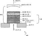
图5示出根据本发明的一个实施例的SEL 500。图5的实施例示出具有集成吸收器的电泵浦增益结构。下镜面504放置在隔离器503上。隔离器503电隔离下镜面504与热沉502。隔离器503包括允许电流在限定的开口中从接触器514a传送到接触器514b、c的开口。增益区510放置在下镜面504上。Figure 5 illustrates an SEL 500 according to one embodiment of the invention. The embodiment of Figure 5 shows an electrically pumped gain structure with an integrated absorber. The lower mirror 504 is placed on the isolator 503 . The isolator 503 electrically isolates the lower mirror 504 from the heat sink 502 . The isolator 503 includes openings that allow current to pass from the contact 514a to the contacts 514b, c in defined openings. The gain region 510 is placed on the lower mirror 504 .
间隔物508放置在增益区510上。在一个实施例中,间隔物508的尺寸在制造时被确定以便对于在接触器514a、b、c之间注入的电流提供足够的长度,以展开来形成在增益部分中有利于基模操作的分布。还要注意,间隔物508的尺寸影响激光腔520的长度和激光输出518的重复率。A spacer 508 is placed on the gain region 510 . In one embodiment, spacer 508 is sized at manufacture to provide sufficient length for current injected between contacts 514a,b,c to expand to form a slit that facilitates fundamental mode operation in the gain section. distributed. Note also that the size of the spacer 508 affects the length of the laser cavity 520 and the repetition rate of the laser output 518 .
吸收器506放置在间隔物508上。AR层512放置在吸收器506上。隔离器503、下镜面504、增益区510、间隔物508、吸收器506和AR层512形成单片增益结构524。Absorber 506 is placed on spacer 508 . AR layer 512 is placed on absorber 506 . Isolator 503 , lower mirror 504 , gain region 510 , spacer 508 , absorber 506 and AR layer 512 form monolithic gain structure 524 .
输出耦合器516放置在AR层512上方并且发射激光输出518。输出耦合器516和下镜面504限定了激光腔520。热沉502在隔离器503下方与SEL 500耦合。SEL 500经由耦合到下镜面504的接触器514a和耦合到间隔物508的接触器514b和514c进行电泵浦。An output coupler 516 is placed over the AR layer 512 and emits a laser output 518 . Output coupler 516 and lower mirror 504 define laser cavity 520 . Heat sink 502 is coupled to SEL 500 below isolator 503. SEL 500 is electrically pumped via contact 514a coupled to lower mirror 504 and contacts 514b and 514c coupled to spacer 508.
图6示出根据本发明的一个实施例的SEL 600。图6的实施例示出具有集成吸收器和用于调谐吸收器的分离的电接触器的电泵浦浦增益结构。下镜面604放置在隔离器603上。吸收器606放置在下镜面604上。Figure 6 illustrates an SEL 600 according to one embodiment of the invention. The embodiment of Figure 6 shows an electrically pumped gain structure with an integrated absorber and separate electrical contacts for tuning the absorber. The lower mirror 604 is placed on the isolator 603 . The absorber 606 is placed on the lower mirror 604 .
电流孔层613放置在吸收器606上。接触器611a和611b允许使用电信号改变吸收器的饱和通量。电流孔层613电隔离吸收器606与增益区610,并且包括允许电流在限定的开口中从接触器614a传送到接触器611a、b的开口。电流孔层对于激光波长是透明的,以允许光在腔620的镜面之间通过。A current hole layer 613 is placed on the absorber 606 . Contactors 611a and 611b allow changing the saturation flux of the absorber using an electrical signal. The current hole layer 613 electrically isolates the absorber 606 from the gain region 610 and includes openings that allow current to pass from the contact 614a to the contacts 611a,b in the defined openings. The current hole layer is transparent to the laser wavelength to allow light to pass between the mirrors of cavity 620 .
增益区610放置在电流孔613上。AR层612放置在增益区610上。隔离器603、下镜面604、吸收器606、电流孔613、增益区610和AR层612形成单片增益结构624。Gain region 610 is placed on current via 613 . AR layer 612 is placed on gain region 610 . The isolator 603 , lower mirror 604 , absorber 606 , current hole 613 , gain region 610 and AR layer 612 form a monolithic gain structure 624 .
输出耦合器616放置在AR层612上方并且发射激光输出618。输出耦合器616和下镜面604限定了激光腔620。热沉602在隔离器603下方与SEL 600耦合。SEL 600经由耦合到下镜面604的接触器614a和耦合到AR层612的接触器614b与614c进行电泵浦。吸收器606可经由耦合到下镜面604的接触器614a和耦合到吸收器层606的接触器611a与611b进行电调谐。An output coupler 616 is placed over the AR layer 612 and emits a laser output 618 . Output coupler 616 and lower mirror 604 define laser cavity 620 . Heat sink 602 is coupled to SEL 600 below isolator 603. SEL 600 is electrically pumped via contact 614a coupled to lower mirror 604 and contacts 614b and 614c coupled to AR layer 612. The absorber 606 is electrically tunable via a contact 614 a coupled to the lower mirror 604 and contacts 611 a and 611 b coupled to the absorber layer 606 .
图7示出根据本发明的一个实施例的SEL 700。图7的实施例示出具有集成吸收器的电泵浦增益结构,其采用介电涂覆的集成微透镜作为输出耦合器。下镜面704放置在隔离器703上。增益区710放置在下镜面704上。吸收器706放置在增益区710上。间隔物709放置在吸收器706上。单片增益结构724包括隔离器703、下镜面704、增益区710、吸收器706和间隔物709。Figure 7 illustrates an SEL 700 according to one embodiment of the invention. The embodiment of Figure 7 shows an electrically pumped gain structure with an integrated absorber that employs a dielectric coated integrated microlens as the output coupler. The lower mirror 704 is placed on the isolator 703 . The gain region 710 is placed on the lower mirror 704 . Absorber 706 is placed on gain region 710 . A spacer 709 is placed on the absorber 706 . Monolithic gain structure 724 includes isolator 703 , lower mirror 704 , gain region 710 , absorber 706 and spacer 709 .
在一个实施例中,单片增益结构724在间隔物709上生长。间隔物709包括诸如砷化镓(GaAs)之类的衬底。参考图7,层将从间隔物709开始、然后是吸收器706等等一直到隔离器703向下生长。在单片结构724生成后,可添加附加层例如间隔物715以完成SEL 700的生产。In one embodiment, monolithic gain structure 724 is grown on spacer 709 . The spacer 709 includes a substrate such as gallium arsenide (GaAs). Referring to FIG. 7 , the layers will grow down starting with spacers 709 , then absorbers 706 and so on until spacers 703 . After the monolithic structure 724 is created, additional layers such as spacers 715 can be added to complete the production of the SEL 700.
折射率匹配层711可放置在间隔物709上。折射率匹配层711避免在腔内部的激光的附加反射。它也提供间隔物715到接触器714b、c和间隔物709的刚性附着。An index matching layer 711 may be placed on the spacer 709 . The index matching layer 711 avoids additional reflection of the laser light inside the cavity. It also provides rigid attachment of spacer 715 to contacts 714b, c and spacer 709 .
间隔物715放置在折射率匹配层711上。间隔物709和715的尺寸可在制造时调整以便实现激光腔720的期望的腔长度。在SEL 700的可替换实施例中,间隔物715不被附着,以使微透镜716放置在折射率匹配层711上。在另一个实施例中,间隔物709在制造期间被移除以使折射率匹配层711放置在吸收器706上。A spacer 715 is placed on the index matching layer 711 . The dimensions of spacers 709 and 715 can be adjusted at the time of manufacture in order to achieve a desired cavity length for laser cavity 720 . In an alternative embodiment of the SEL 700, the spacers 715 are not attached so that the microlenses 716 are placed on the index matching layer 711. In another embodiment, the spacer 709 is removed during fabrication to place the index matching layer 711 on the absorber 706 .
微透镜716放置在间隔物715上。激光输出718从微透镜716发出。微透镜716可被涂覆以提供激光波长的足够反射。激光腔720由下镜面704和微透镜716来限定。热沉702在隔离器703下方与SEL 700耦合。电泵浦经由耦合到下镜面704的接触器714a和耦合到折射率匹配层711的接触器714b与714c被提供给SEL 700。Microlenses 716 are placed on spacers 715 . Laser output 718 emerges from microlens 716 . Microlens 716 may be coated to provide sufficient reflection of the laser wavelength. Laser cavity 720 is defined by lower mirror 704 and microlens 716 . Heat sink 702 is coupled to SEL 700 below isolator 703. Electrical pumping is provided to SEL 700 via contact 714a coupled to lower mirror 704 and contacts 714b and 714c coupled to index matching layer 711.
图8示出根据本发明的一个实施例的SEL 800。图8的实施例示出具有集成吸收器的电泵浦增益结构,其采用由同一衬底制造的介电涂覆的集成微透镜作为增益结构。下镜面804放置在隔离器803上。增益区810放置在下镜面804上。吸收器806放置在增益区810上。Figure 8 illustrates an
包括微透镜816的间隔物809放置在吸收器806上。在SEL 800中,微透镜816由用来生长单片增益结构824的同一片衬底形成。微透镜的顶部形状使用本领域周知的工艺进行蚀刻。微透镜816可被涂覆以提供激光波长的足够反射。如上面结合图7所述,间隔物809的尺寸可生长或蚀刻以实现期望的腔长度。A spacer 809 comprising microlenses 816 is placed on the absorber 806 . In
激光腔820由下镜面804和微透镜816来限定。热沉802在隔离器803下方与SEL 800耦合。电泵浦经由耦合到下镜面804的接触器814a和耦合到间隔物809的接触器814b与814c被提供给SEL 800。在操作中,被动锁模激光输出818从微透镜816发出。
SEL 800提供可进行电泵浦的简单线性腔。SEL 800可生成有高重复率的被动锁模激光输出。在一个实施例中,SEL 800可产生50-100GHz信号。SEL 800是完全集成的,从而导致小尺寸,并且具有晶片水平高容量制造的好处。在一个实施例中,SEL 800采用GaAs MBE制造。The
图9A说明具有集成吸收器的电泵浦SEL的阵列900的一个实施例。阵列900包括SEL 930和SEL 940。热沉902可耦合至SEL 930和940的底部。在其它实施例中,阵列900可包括附加的SEL。Figure 9A illustrates one embodiment of an
SEL 930和SEL 940共用下面的层。下镜面904放置在隔离器903上。增益区910放置在下镜面904上。吸收器906放置在增益区910上。间隔物909放置在吸收器906上。在一个实施例中,SEL 930和SEL 940可彼此电隔离。在一种情况下,这样的隔离可通过在SEL 930和SEL 940之间进行蚀刻来实现。The
SEL 930包括下面的层。折射率匹配层911放置在间隔物909上。间隔物915放置在折射率匹配层911上。微透镜916放置在间隔物915上。激光输出918从微透镜916发出。电泵浦经由耦合到下镜面904的接触器914a和耦合到折射率匹配层911的接触器914b与914c被提供给SEL 930。The
SEL 940包括下面的层。折射率匹配层922放置在间隔物909上。间隔物925放置在折射率匹配层922上。微透镜924放置在间隔物925上。激光输出926从微透镜924发出。电泵浦经由耦合到下镜面904的接触器920a和耦合到折射率匹配层922的接触器920b与920c被提供给SEL 940。The
在一个实施例中,SEL 930和SEL 940是可单独寻址的。耦合到阵列900的控制器(未示出)可提供对每个SEL的控制。在一个实施例中,电泵浦只提供给寻址SEL。在另一个实施例中,间隔物915和925可以是不同的尺寸。在这种情况下,SEL 930的腔长度与SEL 940的腔长度不同,以使SEL 930和940产生具有不同重复率的输出。In one embodiment,
图9B示出二维阵列950的实施例。阵列950包括SEL 951-956,其中至少一个SEL具有如在此所述的集成吸收器。在一个实施例中,每个SEL 951-956是可单独寻址的。在另一个实施例中,每个SEL951-956被配置成以唯一的重复率提供被动锁模输出。在又一个实施例中,每个SEL 951-956被配置成以唯一的功率水平提供被动锁模输出。FIG. 9B shows an embodiment of a two-
图10示出通信系统1000的实施例。光发送器1001包括与多路复用器1003光耦合的SEL阵列1002。SEL阵列1002包括至少一个具有如在此所述的集成吸收器的SEL。多路复用器1003包括选择输入和数据输入。选择输入用于选择SEL阵列1002的SEL。数据输入用于接收调制光发送器1001的输出的数据。可调谐发送器1001输出光信号给与光发送器1001光耦合的光通道1004。在一个实施例中,光信号包括光时分复用(OTDM)信号。光通道1004与网络1006光耦合。在一个实施例中,网络1006是光子分组交换网络。网络1006与光通道1008光耦合。光接收器1010与光通道1008光耦合以接收光信号。在一个实施例中,光通道1004和1008包括光纤。FIG. 10 illustrates an embodiment of a
图11示出计算机系统1100的一个实施例。计算机系统1100包括经由总线1101与处理器1104和存储设备1105耦合的芯片组1102。计算机系统1100还包括系统时钟1 106以提供时钟信号给芯片组1102、处理器1104、存储器1105和总线1101。在另一个实施例中,系统时钟1106只提供时钟信号给处理器1104。在一个实施例中,系统时钟1106输出时钟信号以作为光信号。在其它实施例中,系统时钟1106的时钟信号作为电信号被输出。One embodiment of a computer system 1100 is shown in FIG. 11 . Computer system 1100 includes chipset 1102 coupled to processor 1104 and storage device 1105 via bus 1101 . Computer system 1100 also includes system clock 1 106 to provide clock signals to chipset 1102, processor 1104, memory 1105 and bus 1101. In another embodiment, the system clock 1106 only provides a clock signal to the processor 1104 . In one embodiment, the system clock 1106 outputs the clock signal as an optical signal. In other embodiments, the clock signal of the system clock 1106 is output as an electrical signal.
系统时钟1106包括如在此所述的具有集成吸收器的SEL 1108以用作系统时钟1106的振荡器。在一个实施例中,系统时钟1106可以以10 GHz或更快操作。在另一个实施例中,系统时钟1106可包括一个或多个分频器或一个或多个倍频器,以提供时钟信号给与系统时钟1106耦合的部件。The system clock 1106 includes a SEL 1108 with an integrated sink as described herein for use as an oscillator for the system clock 1106. In one embodiment, system clock 1106 may operate at 10 GHz or faster. In another embodiment, the system clock 1106 may include one or more frequency dividers or one or more frequency multipliers to provide clock signals to components coupled to the system clock 1106 .
图12说明根据本发明的一个实施例的具有量子点半导体可饱和吸收镜(SESAM)1202的固态激光器1200。通常,SESAM调制激光腔中的增益以作为强度的函数。这被动地锁模该激光器。吸收器镜面1202包括一个或多个量子点层,如上所述,其给予吸收器镜面1202低的饱和通量。Figure 12 illustrates a solid state laser 1200 with a quantum dot semiconductor saturable absorber mirror (SESAM) 1202 according to one embodiment of the invention. In general, SESAMs modulate the gain in the laser cavity as a function of intensity. This passively mode locks the laser. The absorber mirror 1202 includes one or more layers of quantum dots, which, as described above, give the absorber mirror 1202 a low saturation flux.
固态激光器1200包括激光介质1204和输出耦合器1206。激光介质1204包括Er:Yb(掺铒镱)、Er:glass(掺铒玻璃)、Nd:Vanadate(掺钕钒酸盐)、Nd:YAG(掺钕钇铝石榴石(Y3Al5O12))、Nd:glass(掺钕玻璃)或类似物。在图12的实施例中,固态激光器1200由二极管泵浦源(未示出)来泵浦。Solid state laser 1200 includes a lasing medium 1204 and an output coupler 1206 . The laser medium 1204 includes Er:Yb (erbium-doped ytterbium), Er:glass (erbium-doped glass), Nd:Vanadate (Nd-doped vanadate), Nd:YAG (Nd-doped yttrium aluminum garnet (Y3 Al5 O12 )), Nd:glass (neodymium-doped glass) or similar. In the embodiment of FIG. 12, solid state laser 1200 is pumped by a diode pump source (not shown).
在固态激光器中采用具有低饱和通量的量子点吸收器1202简化了腔设计,因为大大放宽了对在增益与吸收器材料之间的模尺寸比的要求。另外,可通过增大在吸收器上的模尺寸来大大减少吸收器发热,尤其是以高重复率和对于高的平均功率。The use of quantum dot absorbers 1202 with low saturation fluence in solid-state lasers simplifies cavity design because the requirements on the mode size ratio between gain and absorber materials are greatly relaxed. Additionally, absorber heating can be greatly reduced by increasing the mode size on the absorber, especially at high repetition rates and for high average powers.
图13说明具有集成到固态激光介质1304中的量子点半导体可饱和吸收镜1302的固态激光器1300。激光介质1304包括与上面结合激光介质1204所述的类似的介质。激光介质1304包括曲面反射器1306。量子点半导体可饱和吸收镜1302包括包含半导体布拉格堆栈的高反射器和一个或多个被透明间隔物层分离的量子点吸收器层。选择间隔物层的厚度,以对于光驻波效应(共振或反共振)调整总结构的光厚度。FIG. 13 illustrates a
所说明的本发明实施例的上面的描述,包括在摘要中所描述的内容,并不打算是穷举的或者把本发明限制于所公开的精确形式。尽管此处为了说明的目的描述了本发明的特定实施例和例子,但是正如相关领域的技术人员将认识到的,在本发明范围内的各种等效修改是可能的。The above description of illustrated embodiments of the invention, including what is described in the Abstract, is not intended to be exhaustive or to limit the invention to the precise forms disclosed. While specific embodiments of, and examples for, the invention are described herein for illustrative purposes, various equivalent modifications are possible within the scope of the invention, as those skilled in the relevant art will recognize.
根据上面的详细描述,可以对本发明的实施例进行这些改变。在后面的权利要求书中所采用的术语不应解释为将本发明限定在说明书和权利要求中所公开的特定实施例。而是,本发明的范围将由后面的权利要求书来确定,该权利要求书将根据建立的权利要求解释的原则来解释。These changes can be made to the embodiments of the invention in light of the above detailed description. The terms used in the following claims should not be construed to limit the invention to the specific embodiments disclosed in the specification and claims. Rather, the scope of the invention is to be determined by the following claims, which are to be interpreted in accordance with established doctrines of claim interpretation.
Claims (7)
Applications Claiming Priority (3)
| Application Number | Priority Date | Filing Date | Title |
|---|---|---|---|
| US10/814,050 | 2004-03-31 | ||
| US10/814,050US20060029112A1 (en) | 2004-03-31 | 2004-03-31 | Surface emitting laser with an integrated absorber |
| PCT/US2005/010400WO2005098573A1 (en) | 2004-03-31 | 2005-03-25 | Surface emitting laser with an integrated absorber |
Publications (2)
| Publication Number | Publication Date |
|---|---|
| CN1950781A CN1950781A (en) | 2007-04-18 |
| CN1950781Btrue CN1950781B (en) | 2011-04-20 |
Family
ID=34964379
Family Applications (1)
| Application Number | Title | Priority Date | Filing Date |
|---|---|---|---|
| CN2005800107807AExpired - Fee RelatedCN1950781B (en) | 2004-03-31 | 2005-03-25 | Surface-emitting lasers with integrated absorbers |
Country Status (7)
| Country | Link |
|---|---|
| US (2) | US20060029112A1 (en) |
| EP (1) | EP1735681B1 (en) |
| JP (1) | JP5237631B2 (en) |
| CN (1) | CN1950781B (en) |
| AT (1) | ATE442687T1 (en) |
| DE (1) | DE602005016536D1 (en) |
| WO (1) | WO2005098573A1 (en) |
Families Citing this family (35)
| Publication number | Priority date | Publication date | Assignee | Title |
|---|---|---|---|---|
| US7860143B2 (en)* | 2004-04-30 | 2010-12-28 | Finisar Corporation | Metal-assisted DBRs for thermal management in VCSELs |
| US7309953B2 (en)* | 2005-01-24 | 2007-12-18 | Principia Lightworks, Inc. | Electron beam pumped laser light source for projection television |
| KR101100434B1 (en)* | 2005-05-07 | 2011-12-30 | 삼성전자주식회사 | External resonator type surface emitting laser with rear light pumping |
| US7526009B2 (en)* | 2005-05-07 | 2009-04-28 | Samsung Electronics Co., Ltd. | End-pumped vertical external cavity surface emitting laser |
| DE102005056949B4 (en)* | 2005-09-30 | 2013-08-22 | Osram Opto Semiconductors Gmbh | Optically pumped surface emitting semiconductor laser and optical projection device with such a semiconductor laser |
| WO2007071809A1 (en)* | 2005-12-22 | 2007-06-28 | Reflekron Oy | Semiconductor device and method to fabricate thereof |
| US7801197B2 (en)* | 2006-06-16 | 2010-09-21 | Epicrystals Oy | High power laser device |
| JP2008028379A (en)* | 2006-06-22 | 2008-02-07 | Fujifilm Corp | Mode-locked laser device |
| EP1870972A1 (en)* | 2006-06-22 | 2007-12-26 | Fujifilm Corporation | Mode-locked laser device |
| US8102893B2 (en)* | 2007-06-14 | 2012-01-24 | Necsel Intellectual Property | Multiple emitter VECSEL |
| DE102008030818B4 (en)* | 2008-06-30 | 2022-03-03 | OSRAM Opto Semiconductors Gesellschaft mit beschränkter Haftung | Surface emitting semiconductor laser with multiple active zones |
| US9124064B2 (en) | 2010-05-28 | 2015-09-01 | Daniel Kopf | Ultrashort pulse microchip laser, semiconductor laser, and pump method for thin laser media |
| US8432551B2 (en) | 2010-08-06 | 2013-04-30 | Honeywell International Inc. | Neon or iodine absorption enhanced hene ring laser gyroscope |
| WO2012068563A1 (en)* | 2010-11-19 | 2012-05-24 | Trilumina Corporation | Optical pumping of solid-state laser material using addressable laser array |
| US9025635B2 (en) | 2011-01-24 | 2015-05-05 | Soraa Laser Diode, Inc. | Laser package having multiple emitters configured on a support member |
| US9595813B2 (en) | 2011-01-24 | 2017-03-14 | Soraa Laser Diode, Inc. | Laser package having multiple emitters configured on a substrate member |
| US8687198B2 (en) | 2011-09-20 | 2014-04-01 | Honeywell International Inc. | Coupled cavity dispersion enhanced ring laser gyroscope |
| CN102593720A (en)* | 2012-03-19 | 2012-07-18 | 中国科学院福建物质结构研究所 | Locked mode semiconductor laser based on quantum dot-quantum well mixed structure |
| US9124062B2 (en)* | 2012-03-22 | 2015-09-01 | Palo Alto Research Center Incorporated | Optically pumped surface emitting lasers incorporating high reflectivity/bandwidth limited reflector |
| US9112331B2 (en) | 2012-03-22 | 2015-08-18 | Palo Alto Research Center Incorporated | Surface emitting laser incorporating third reflector |
| US9065241B2 (en)* | 2012-05-11 | 2015-06-23 | Massachusetts Institute Of Technology | Methods, systems, and apparatus for high energy optical-pulse amplification at high average power |
| US9112332B2 (en) | 2012-06-14 | 2015-08-18 | Palo Alto Research Center Incorporated | Electron beam pumped vertical cavity surface emitting laser |
| JP6245629B2 (en)* | 2013-03-26 | 2017-12-13 | 大学共同利用機関法人自然科学研究機構 | In-vehicle ignition system using semiconductor laser pumped solid-state laser device |
| DE102014205022B4 (en)* | 2014-03-18 | 2025-01-16 | Fraunhofer-Gesellschaft zur Förderung der angewandten Forschung e.V. | Optically pumped semiconductor disk laser |
| WO2016049787A1 (en) | 2014-10-02 | 2016-04-07 | ETH Zürich | Pulsed laser |
| US10447004B2 (en)* | 2015-11-19 | 2019-10-15 | Nlight, Inc. | Laser fault tolerance and self-calibration system |
| WO2018093435A2 (en)* | 2016-09-12 | 2018-05-24 | Arizona Board Of Regents On Behalf Of The University Of Arizona | Nonequilibrium pulsed femtosecond semiconductor disk laser with non-equidistant mqw structure |
| EP3573103B1 (en)* | 2017-02-03 | 2021-01-06 | Huawei Technologies Co., Ltd. | Photoelectric conversion apparatus |
| EP3419050A1 (en) | 2017-06-23 | 2018-12-26 | ams International AG | Radiation-hardened package for an electronic device and method of producing a radiation-hardened package |
| CN110892597B (en)* | 2017-07-18 | 2022-11-04 | 索尼公司 | Light emitting device and light emitting device array |
| GB202009952D0 (en)* | 2020-06-30 | 2020-08-12 | Ams Int Ag | Light source |
| EP4241403A4 (en)* | 2021-01-28 | 2024-04-24 | NewPhotonics Ltd. | SYSTEM FOR PULSED OPTICAL DATA TRANSMISSION WITH RECEIVER RESETTABLE CLOCK |
| EP4131674A1 (en) | 2021-08-06 | 2023-02-08 | ETH Zurich | Radiation source |
| CN115102035A (en)* | 2022-05-19 | 2022-09-23 | 福建慧芯激光科技有限公司 | High-efficiency vertical cavity surface EML chip with micro-lens |
| CN115425519A (en)* | 2022-09-30 | 2022-12-02 | 常州纵慧芯光半导体科技有限公司 | A vertical cavity surface emitting laser and its manufacturing method |
Citations (8)
| Publication number | Priority date | Publication date | Assignee | Title |
|---|---|---|---|---|
| US5062115A (en)* | 1990-12-28 | 1991-10-29 | Xerox Corporation | High density, independently addressable, surface emitting semiconductor laser/light emitting diode arrays |
| US5574738A (en)* | 1995-06-07 | 1996-11-12 | Honeywell Inc. | Multi-gigahertz frequency-modulated vertical-cavity surface emitting laser |
| US5627853A (en)* | 1994-03-16 | 1997-05-06 | Coherent, Inc. | Optimized laser energy conversion through automatic mode matched pumping |
| WO2001059895A1 (en)* | 2000-02-11 | 2001-08-16 | Gigatera Ag | Passively mode-locked optically pumped semiconductor external-cavity surface-emitting laser |
| US20020039376A1 (en)* | 2000-10-04 | 2002-04-04 | Samsung Electronics., Ltd. | Micro-lens built-in vertical cavity surface emitting laser |
| US20020110159A1 (en)* | 2001-02-15 | 2002-08-15 | Aculight Corporation | External frequency conversion of surface-emitting diode lasers |
| US20030113078A1 (en)* | 2001-12-13 | 2003-06-19 | Tatum Jimmy A. | Methods, systems and means for providing data communications between data equipment |
| US6628695B1 (en)* | 2002-03-07 | 2003-09-30 | The Board Of Trustees Of The Leland Stanford Junior University | Monolithically integrated mode-locked vertical cavity surface emitting laser (VCSEL) |
Family Cites Families (23)
| Publication number | Priority date | Publication date | Assignee | Title |
|---|---|---|---|---|
| US4860296A (en)* | 1983-12-30 | 1989-08-22 | American Telephone And Telegraph Company, At&T Bell Laboratories | Laser controlled by a multiple-layer heterostructure |
| US4959540A (en)* | 1989-05-15 | 1990-09-25 | International Business Machines Corporation | Optical clock system with optical time delay means |
| US5216263A (en)* | 1990-11-29 | 1993-06-01 | Xerox Corporation | High density, independently addressable, surface emitting semiconductor laser-light emitting diode arrays |
| US5115441A (en)* | 1991-01-03 | 1992-05-19 | At&T Bell Laboratories | Vertical cavity surface emmitting lasers with transparent electrodes |
| US5287376A (en)* | 1992-12-14 | 1994-02-15 | Xerox Corporation | Independently addressable semiconductor diode lasers with integral lowloss passive waveguides |
| US5724375A (en)* | 1996-07-17 | 1998-03-03 | W. L. Gore & Associates, Inc. | Vertical cavity surface emitting laser with enhanced second harmonic generation and method of making same |
| FR2751796B1 (en)* | 1996-07-26 | 1998-08-28 | Commissariat Energie Atomique | SOILDE MICROLASER, OPTICALLY PUMPED BY VERTICAL CAVITY SEMICONDUCTOR LASER |
| US5991318A (en)* | 1998-10-26 | 1999-11-23 | Coherent, Inc. | Intracavity frequency-converted optically-pumped semiconductor laser |
| US6098264A (en)* | 1999-02-17 | 2000-08-08 | Eastman Kodak Company | Method of assembling laser and modulator unit |
| US6418152B1 (en)* | 2000-02-18 | 2002-07-09 | Trw Inc. | Multi-amplifier, high power mode locked laser |
| US6741619B1 (en)* | 2000-04-03 | 2004-05-25 | Massachusetts Institute Of Technology | Semiconductor elements for stabilizing laser output |
| US20020067882A1 (en)* | 2000-05-26 | 2002-06-06 | Guilfoyle Peter S. | Virtual optoelectronic crossbar switch |
| KR100393057B1 (en)* | 2000-10-20 | 2003-07-31 | 삼성전자주식회사 | Vertical cavity surface emitting laser having micro-lens |
| US6710911B2 (en)* | 2001-03-02 | 2004-03-23 | Evident Technologies | Optical wavelength converter |
| JP4095306B2 (en)* | 2002-01-18 | 2008-06-04 | 株式会社リコー | Semiconductor light emitting device, manufacturing method thereof, and optical transmission system |
| AU2002322917A1 (en)* | 2001-08-21 | 2003-03-10 | Luxonics Canada Inc. | Suppression of mode-beating noise in a q-switched pulsed laser using novel q-switch device |
| JP2003121611A (en)* | 2001-10-16 | 2003-04-23 | Canon Inc | Lens made of semiconductor material containing Al, surface-type optical element using the same, and method of manufacturing lens |
| JP3830858B2 (en)* | 2002-01-08 | 2006-10-11 | 独立行政法人科学技術振興機構 | Ultra-high-speed, wide-wavelength optical saturable absorber semiconductor, semiconductor device using the same, and waveguide-type optical-optical switch |
| JP2004063957A (en)* | 2002-07-31 | 2004-02-26 | Hitachi Ltd | Method for manufacturing semiconductor member having semiconductor quantum dots, semiconductor laser, and optical module using the same |
| US7339963B2 (en)* | 2002-11-27 | 2008-03-04 | International Business Machines Corporation | High speed data channel including a CMOS VCSEL driver and a high performance photodetector and CMOS photoreceiver |
| GB2399941A (en)* | 2003-03-24 | 2004-09-29 | Univ Strathclyde | Vertical cavity semiconductor optical devices |
| WO2004110943A2 (en)* | 2003-06-19 | 2004-12-23 | Elop Electro-Optics Industries Ltd. | Glass ceramics for laser systems |
| WO2005094275A2 (en)* | 2004-03-25 | 2005-10-13 | Imra America, Inc. | Optical parametric amplification, optical parametric generation, and optical pumping in optical fibers systems |
- 2004
- 2004-03-31USUS10/814,050patent/US20060029112A1/ennot_activeAbandoned
- 2005
- 2005-03-25ATAT05731285Tpatent/ATE442687T1/ennot_activeIP Right Cessation
- 2005-03-25DEDE602005016536Tpatent/DE602005016536D1/ennot_activeExpired - Lifetime
- 2005-03-25EPEP05731285Apatent/EP1735681B1/ennot_activeExpired - Lifetime
- 2005-03-25CNCN2005800107807Apatent/CN1950781B/ennot_activeExpired - Fee Related
- 2005-03-25WOPCT/US2005/010400patent/WO2005098573A1/enactiveApplication Filing
- 2005-03-25JPJP2007503120Apatent/JP5237631B2/ennot_activeExpired - Fee Related
- 2007
- 2007-03-19USUS11/725,659patent/US7729393B2/ennot_activeExpired - Fee Related
Patent Citations (8)
| Publication number | Priority date | Publication date | Assignee | Title |
|---|---|---|---|---|
| US5062115A (en)* | 1990-12-28 | 1991-10-29 | Xerox Corporation | High density, independently addressable, surface emitting semiconductor laser/light emitting diode arrays |
| US5627853A (en)* | 1994-03-16 | 1997-05-06 | Coherent, Inc. | Optimized laser energy conversion through automatic mode matched pumping |
| US5574738A (en)* | 1995-06-07 | 1996-11-12 | Honeywell Inc. | Multi-gigahertz frequency-modulated vertical-cavity surface emitting laser |
| WO2001059895A1 (en)* | 2000-02-11 | 2001-08-16 | Gigatera Ag | Passively mode-locked optically pumped semiconductor external-cavity surface-emitting laser |
| US20020039376A1 (en)* | 2000-10-04 | 2002-04-04 | Samsung Electronics., Ltd. | Micro-lens built-in vertical cavity surface emitting laser |
| US20020110159A1 (en)* | 2001-02-15 | 2002-08-15 | Aculight Corporation | External frequency conversion of surface-emitting diode lasers |
| US20030113078A1 (en)* | 2001-12-13 | 2003-06-19 | Tatum Jimmy A. | Methods, systems and means for providing data communications between data equipment |
| US6628695B1 (en)* | 2002-03-07 | 2003-09-30 | The Board Of Trustees Of The Leland Stanford Junior University | Monolithically integrated mode-locked vertical cavity surface emitting laser (VCSEL) |
Non-Patent Citations (8)
| Title |
|---|
| E. U.Rafailov, S. J. White, A.A. Lagatsky, A.Miller,W.Sibbett.,Cheng Xing, EA. Avrntin,D. A. Livshits, A.E.Zbukov,V. M. Ustinov.Fast quantum-dot saturable absorber forpassivemodelockingof solid-state lasers.Laser and Electro-Optics Society2.2003,2557-558.* |
| E.U.Rafailov S. J. White |
| G. J. Spu¨ hler, S. Reffert, and M. Haiml,M. Moser,U. Kellera,.Output-coupling semiconductor saturable absorber mirror.APPLIED PHYSICS LETTERS78 18.2001,78(18),2733-2735. |
| G. J. Spu¨ hler, S. Reffert, and M. Haiml,M. Moser,U. Kellera,.Output-coupling semiconductor saturable absorber mirror.APPLIED PHYSICS LETTERS78 18.2001,78(18),2733-2735.* |
| Shin Arahira. Yasuhiro Matsui, Yoh Ogawa.Mode-Locking at Very High Repetition Rates More thanTerahertz in Passively Mode-LockedDistributed-Bragg-Reflector Laser Diodes.IEEE JOURNAL Ob QUANTUM ELECTRONICS32 7.1996,32(7),1211-1224. |
| Shin Arahira. Yasuhiro Matsui, Yoh Ogawa.Mode-Locking at Very High Repetition Rates More thanTerahertz in Passively Mode-LockedDistributed-Bragg-Reflector Laser Diodes.IEEE JOURNAL Ob QUANTUM ELECTRONICS32 7.1996,32(7),1211-1224.* |
| Xiaodong Huang,A. Stintz, Hua Li, L. F. Lester, Julian Cheng,K. J. Malloy.Passive mode-locking in 1.3 mm two-section InAs quantumdot lasers.APPLIED PHYSICS LETTERS78 19.2001,78(19),2825-2827. |
| Xiaodong Huang,A. Stintz, Hua Li, L. F. Lester, Julian Cheng,K. J. Malloy.Passive mode-locking in 1.3 mm two-section InAs quantumdot lasers.APPLIED PHYSICS LETTERS78 19.2001,78(19),2825-2827.* |
Also Published As
| Publication number | Publication date |
|---|---|
| WO2005098573A1 (en) | 2005-10-20 |
| JP2007528130A (en) | 2007-10-04 |
| JP5237631B2 (en) | 2013-07-17 |
| US20070189350A1 (en) | 2007-08-16 |
| US7729393B2 (en) | 2010-06-01 |
| EP1735681A1 (en) | 2006-12-27 |
| EP1735681B1 (en) | 2009-09-09 |
| CN1950781A (en) | 2007-04-18 |
| DE602005016536D1 (en) | 2009-10-22 |
| ATE442687T1 (en) | 2009-09-15 |
| US20060029112A1 (en) | 2006-02-09 |
Similar Documents
| Publication | Publication Date | Title |
|---|---|---|
| CN1950781B (en) | Surface-emitting lasers with integrated absorbers | |
| EP1264373B1 (en) | Passively mode-locked optically pumped semiconductor external-cavity surface-emitting laser | |
| JP4487085B2 (en) | Linked cavity high power semiconductor laser | |
| US9124064B2 (en) | Ultrashort pulse microchip laser, semiconductor laser, and pump method for thin laser media | |
| US7801197B2 (en) | High power laser device | |
| EP1606863B1 (en) | Improvements in and relating to vertical-cavity semiconductor optical devices | |
| US6628695B1 (en) | Monolithically integrated mode-locked vertical cavity surface emitting laser (VCSEL) | |
| JPH1084169A (en) | Solid microlaser provided with optical pumping by direct-axis cavity semiconductor laser | |
| Bellancourt et al. | Modelocked integrated external-cavity surface emitting laser | |
| Laurain et al. | Recent advances in power scaling of high-power optically-pumped semiconductor lasers for ultrashort pulse generation and continuous wave single frequency operation | |
| Garnache et al. | Pico-second passively mode locked surface-emitting laser with self-assembled semiconductor quantum dot absorber | |
| Maas et al. | MIXSELs-a new class of ultrafast semiconductor lasers | |
| Wiemer et al. | A single transverse-mode monolithically integrated long vertical-cavity surface-emitting laser | |
| Schwertfeger et al. | High-power picosecond pulse generation due to mode-locking with a monolithic 10-mm-long four-section DBR laser at 920 nm | |
| Wittwer et al. | Modelocked Integrated External-Cavity Surface Emitting Laser (MIXSEL) generates 660 mW average power in 23-ps pulses at 3 GHz repetition rate | |
| Südmeyer | Power scaling of the MIXSEL: an integrated picosecond semiconductor laser with> 6 W average power | |
| CN119890919A (en) | Picosecond pulse source based on harmonic self-mode-locking semiconductor surface-emitting laser | |
| Rudin et al. | Modelocked Integrated External-Cavity Surface Emitting Laser (MIXSEL) with output power up to 660 mW and repetition rate up to 10 GHz | |
| Okhotnikov | Tailoring the wavelength of semiconductor disk lasers | |
| Sirbu et al. | Wafer-fused 1310 nm and 1550 nm mode-locked semiconductor disk lasers | |
| Okhotnikov et al. | Advances in power scalable, tunable, and mode-locked semiconductor disk lasers | |
| Gerster | Semiconductor Disk Laser on Microchannel Cooler | |
| Lorenser et al. | Passively Mode-Locked Surface-Emitting Semiconductor Lasers with High Repetition Rates of up to 30 GHz | |
| Li et al. | High-power InGaAs VCSEL's single devices and 2D arrays |
Legal Events
| Date | Code | Title | Description |
|---|---|---|---|
| C06 | Publication | ||
| PB01 | Publication | ||
| C10 | Entry into substantive examination | ||
| SE01 | Entry into force of request for substantive examination | ||
| C14 | Grant of patent or utility model | ||
| GR01 | Patent grant | ||
| CF01 | Termination of patent right due to non-payment of annual fee | Granted publication date:20110420 | |
| CF01 | Termination of patent right due to non-payment of annual fee |