CN1947107A - Device for transmitting data between memories - Google Patents
Device for transmitting data between memoriesDownload PDFInfo
- Publication number
- CN1947107A CN1947107ACNA2004800410725ACN200480041072ACN1947107ACN 1947107 ACN1947107 ACN 1947107ACN A2004800410725 ACNA2004800410725 ACN A2004800410725ACN 200480041072 ACN200480041072 ACN 200480041072ACN 1947107 ACN1947107 ACN 1947107A
- Authority
- CN
- China
- Prior art keywords
- memory
- command
- fcdp
- mpc
- controller
- Prior art date
- Legal status (The legal status is an assumption and is not a legal conclusion. Google has not performed a legal analysis and makes no representation as to the accuracy of the status listed.)
- Granted
Links
Images


Classifications
- G—PHYSICS
- G06—COMPUTING OR CALCULATING; COUNTING
- G06F—ELECTRIC DIGITAL DATA PROCESSING
- G06F13/00—Interconnection of, or transfer of information or other signals between, memories, input/output devices or central processing units
- G06F13/14—Handling requests for interconnection or transfer
- G06F13/20—Handling requests for interconnection or transfer for access to input/output bus
- G06F13/28—Handling requests for interconnection or transfer for access to input/output bus using burst mode transfer, e.g. direct memory access DMA, cycle steal
Landscapes
- Engineering & Computer Science (AREA)
- Theoretical Computer Science (AREA)
- Physics & Mathematics (AREA)
- General Engineering & Computer Science (AREA)
- General Physics & Mathematics (AREA)
- Techniques For Improving Reliability Of Storages (AREA)
- Read Only Memory (AREA)
- Communication Control (AREA)
Abstract
Translated fromChinese
Description
Translated fromChinese技术领域technical field
本发明涉及一种用于在存储器间传输数据的装置,如权利要求1中前序特征语句中声称的那样。The invention relates to a device for transferring data between memories as claimed in the preamble characterizing clause of
背景技术Background technique
在微处理器系统中,大量数据必须经常在易失性存储器和非易失性存储器之间传输。当使用易失性存储器中的程序时存取速度通常是较高的,并且因此当系统启动时,为了获得较高的运行速度,数据通常会从非易失性存储器传输到易失性存储器中。当程序正在运行时,为了最优化使用有限的易失性存储器和/或在供电故障时确保保护数据,数据同样在易失性存储器和非易失性存储器之间传输。In microprocessor systems, large amounts of data must frequently be transferred between volatile and nonvolatile memory. Access speed is usually higher when using programs in volatile memory, and therefore when the system starts up, data is usually transferred from non-volatile memory to volatile memory in order to achieve higher operating speed . Data is also transferred between volatile and non-volatile memory while the program is running, in order to optimize the use of the limited volatile memory and/or to ensure protection of the data in the event of a power failure.
存储器访问高度地取决于所使用的存储器的类型。例如向易失性异步RAM中存取相对是简单的。其他存储器装置,如非易失性NAND闪存装置,就需要相对复杂的存取协议。具有NAND结构的非易失性存储器装置,例如InfineonNROM,目前普遍地变得更加显著地重要,确切地说是由于移动设备如数字照相机、移动电话、PDA或笔记本电脑上不断增加的存储器需求和其非常低的价格。对那些最后提到的存储器装置的随机存取是非常慢的并且需要在运行程序前将程序和数据传送到更快的易失性存储器(VM)。由于它们的内部结构,读或写相对较大的数据块是最优化的数据传送模式,例如此相对较大的数据块可以是存储页。为了读取访问,在输出读取命令和页地址给NAND闪存装置之后,首先将数据传送到装置中的缓冲器中,并且此通常需要十分之几微秒的传输时间。当NAND闪存装置发信号表示此传输完成,所有页数据(512或2048字节)可以以每秒40MB的高数据速度传送到易失性存储器中。进一步,NAND闪存装置具有比特误差的倾向,在数据传送到易失性存储器前其需要比特误差检测和比特误差校正。Memory access is highly dependent on the type of memory used. For example, accessing volatile asynchronous RAM is relatively simple. Other memory devices, such as non-volatile NAND flash memory devices, require relatively complex access protocols. Non-volatile memory devices with a NAND structure, such as Infineon NROM, are generally becoming significantly more important these days, precisely due to the ever-increasing memory requirements and other very low price. Random access to those last-mentioned memory devices is very slow and requires transferring programs and data to faster volatile memory (VM) before running the program. Due to their internal structure, reading or writing relatively large data blocks, such as memory pages, is the most optimized data transfer mode. For a read access, after outputting a read command and a page address to a NAND flash device, the data is first transferred into a buffer in the device, and this usually requires a transfer time of a few tenths of microseconds. When the NAND flash device signals that the transfer is complete, all page data (512 or 2048 bytes) can be transferred to volatile memory at a high data rate of 40MB per second. Further, NAND flash memory devices are prone to bit errors, which require bit error detection and bit error correction before data is transferred to volatile memory.
在VM和非易失性存储器(NVM)之间传送的数据以最高可能速度完成以最小化系统启动时间。进一步,当微处理器运行程序时,为了允许程序和数据的动态加载,数据传输时可能的。进一步,微处理器的运行中的数据传送的影响将被最小化。理想地,微处理器在易失性存储器中存储数据传输任务的列表,并仅在这些任务被全部完成以后微处理器才能被中断。Data transfers between the VM and non-volatile memory (NVM) are done at the highest possible speed to minimize system startup time. Further, data transfer is possible in order to allow dynamic loading of programs and data while the microprocessor is running the program. Further, the impact of data transfers on-the-fly by the microprocessor will be minimized. Ideally, the microprocessor stores a list of data transfer tasks in volatile memory, and the microprocessor can be interrupted only after these tasks have all been completed.
在存储器之间的数据传输通常使用直接存储器存取控制器(DMAC)执行。然而,DMAC局限于简单的存取类型并且不能适应更加复杂数据传输协议。在后面的示例中,由微控制器来控制数据传输。Data transfer between memories is typically performed using a direct memory access controller (DMAC). However, DMAC is limited to simple access types and cannot adapt to more complex data transfer protocols. In the latter example, the data transfer is controlled by a microcontroller.
发明内容Contents of the invention
本发明基于提供一种在存储器之间尽可能快地传送数据的装置的目的,并且该装置可以适应更复杂的数据传输协议,但在处理过程中需要尽可能少的硬件,并且具有灵活地匹配广泛不同操作条件的能力。The present invention is based on the object of providing a device for transferring data between memories as quickly as possible, and which can accommodate more complex data transfer protocols, but requires as little hardware as possible during processing, and has the flexibility to match Capability for a wide variety of operating conditions.
根据本发明,通过如权利要求1中所声称的装置来达到此目的。According to the invention, this object is achieved by a device as claimed in
根据本发明的装置的有利的和优选的实施例是权利要求2至20的主旨。Advantageous and preferred embodiments of the device according to the invention are the subject-matter of
本发明的实质是仅使用专用数据传输控制器而不需要额外的装置,因此全部的硬件就最小化,并且现有的硬件可以再使用,如DMAC或传统的存储器控制器。进一步,由于在硬件中仅执行一种基本的传输协议而使得适应性变得最大化。使用一个或同样的硬件结构,所有对不同应用的进一步适应可以由软件来执行。与现有技术相比,其中各自附加的特定的数据传输控制器由专用硬件来匹配各自特定的应用需求,此增加了产品的适应性,因此对降低成本作出了相当大的贡献。The essence of the present invention is to use only a dedicated data transfer controller without additional devices, so the overall hardware is minimized and existing hardware can be reused, such as DMAC or conventional memory controllers. Further, flexibility is maximized since only one basic transport protocol is implemented in hardware. Using one or the same hardware structure, all further adaptations to different applications can be performed by software. Compared with the prior art, in which each additional specific data transmission controller is matched with each specific application requirement by dedicated hardware, this increases the adaptability of the product, thus making a considerable contribution to cost reduction.
附图说明Description of drawings
根据本发明的装置的有利的和优选的示范实施例将在下文中参考附图说明,其中:Advantageous and preferred exemplary embodiments of the device according to the invention will be described hereinafter with reference to the accompanying drawings, in which:
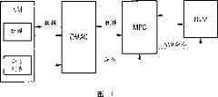
图1示出了根据本发明具有直接存储器存取控制器的装置的第一示范实施例的结构示意图,FIG. 1 shows a schematic structural diagram of a first exemplary embodiment of a device with a direct memory access controller according to the present invention,
图2示出了根据本发明使用直接存储器存取控制器和传统存储器控制器的装置的第二示范实施例的结构示意图,FIG. 2 shows a schematic structural diagram of a second exemplary embodiment of an apparatus using a direct memory access controller and a conventional memory controller according to the present invention,
图3用示意图示出了NAND闪存写操作的数据流,Figure 3 schematically shows the data flow of the NAND flash write operation,
图4用示意图示出了NAND闪存读操作的数据流,Figure 4 schematically shows the data flow of the NAND flash read operation,
图5示出了闪存控制直接存储器存取端口(FCDP)的一个示范实施例的结构示意图,FIG. 5 shows a schematic structural diagram of an exemplary embodiment of a flash control direct memory access port (FCDP),
图6示出了NAND闪存接口的一个示范实施例,Figure 6 shows an exemplary embodiment of a NAND flash interface,
图7用示意图示出了FCDP保护构造的一个示范实施例,Figure 7 schematically shows an exemplary embodiment of the FCDP protection structure,
图8用示意图示出了具有(512+16)×8位页大小的NAND闪存页构造的第一示范实施例,FIG. 8 schematically shows a first exemplary embodiment of a NAND flash page structure with a page size of (512+16)×8 bits,
图9用示意图示出了具有(2048+64)×8位页大小的NAND闪存页构造的第二示范实施例,FIG. 9 schematically shows a second exemplary embodiment of a NAND flash page structure with a page size of (2048+64)×8 bits,
图10用示意图示出了根据图5中所示FCDP示范实施例的FCDP_NFECCCONFIG寄存器,而在这样情况下相关寄存器字段的描述可以在表4中发现,Figure 10 schematically shows the FCDP_NFECCCONFIG register according to the exemplary embodiment of FCDP shown in Figure 5, while in this case the description of the relevant register fields can be found in Table 4,
图11用示意图示出了根据图5中所示FCDP示范实施例的FCDP_MECCPTR寄存器,而在这样情况下相关寄存器字段的描述可以在表5中发现,Figure 11 schematically shows the FCDP_MECCPTR register according to the exemplary embodiment of FCDP shown in Figure 5, while the description of the relevant register fields in this case can be found in Table 5,
图12用示意图示出了根据图5中所示FCDP示范实施例的FCDP_NFSECCPTR寄存器,而在这样情况下相关寄存器字段的描述可以在表6中发现,Figure 12 schematically shows the FCDP_NFSECCPTR register according to the exemplary embodiment of FCDP shown in Figure 5, while the description of the relevant register fields in this case can be found in Table 6,
图13用示意图示出了根据图5中所示FCDP示范实施例的FCDP_NFIECCPTR寄存器,而在这样情况下相关寄存器字段的描述可以在表7中发现,Figure 13 schematically shows the FCDP_NFIECCPTR register according to the exemplary embodiment of FCDP shown in Figure 5, while the description of the relevant register fields in this case can be found in Table 7,
图14用示意图示出了根据图5中所示FCDP示范实施例的FCDP_NFMECCST寄存器,而在这样情况下相关寄存器字段的描述可以在表8中发现,Figure 14 schematically shows the FCDP_NFMECCST register according to the exemplary embodiment of the FCDP shown in Figure 5, while the description of the relevant register fields in this case can be found in Table 8,
图15用示意图示出了根据图5中所示FCDP示范实施例的FCDP_NFSECCST寄存器,而在这样情况下相关寄存器字段的描述可以在表9中发现,Figure 15 schematically shows the FCDP_NFSECCST register according to the exemplary embodiment of FCDP shown in Figure 5, while in this case the description of the relevant register fields can be found in Table 9,
图16示出了保护机构的一个示范实施例的程序运行方案,Figure 16 shows a program operation scheme of an exemplary embodiment of the protection mechanism,
图17用示意图示出了根据图5中所示FCDP示范实施例的FCDP_NFPASSWD寄存器,而在这样情况下相关寄存器字段的描述可以在表10中发现,Figure 17 schematically shows the FCDP_NFPASSWD register according to the exemplary embodiment of FCDP shown in Figure 5, while the description of the relevant register fields in this case can be found in Table 10,
图18用示意图示出了根据图5中所示FCDP示范实施例的FCDP_NFPROTCMD寄存器,而在这样情况下相关寄存器字段的描述可以在表11中发现,Figure 18 schematically shows the FCDP_NFPROTCMD register according to the exemplary embodiment of FCDP shown in Figure 5, while the description of the relevant register fields in this case can be found in Table 11,
图19用示意图示出了根据图5中所示FCDP示范实施例的FCDP_NFADDRWIN1L寄存器,而在这样情况下相关寄存器字段的描述可以在表12中发现,Figure 19 schematically shows the FCDP_NFADDRWIN1L register according to the exemplary embodiment of the FCDP shown in Figure 5, while the description of the relevant register fields in this case can be found in Table 12,
图20用示意图示出了根据图5中所示FCDP示范实施例的FCDP_NFADDRWIN1H寄存器,而在这样情况下相关寄存器字段的描述可以在表13中发现,Figure 20 schematically shows the FCDP_NFADDRWIN1H register according to the exemplary embodiment of FCDP shown in Figure 5, while in this case the description of the relevant register fields can be found in Table 13,
图21用示意图示出了根据图5中所示FCDP示范实施例的FCDP_NFADDRWIN2L寄存器,而在这样情况下相关寄存器字段的描述可以在表14中发现,和Figure 21 schematically shows the FCDP_NFADDRWIN2L register according to the FCDP exemplary embodiment shown in Figure 5, while in this case the description of the relevant register fields can be found in Table 14, and
图22用示意图示出了根据图5中所示FCDP示范实施例的FCDP_NFADDRWIN2H寄存器,而在这样情况下相关寄存器字段的描述可以在表15中发现。FIG. 22 schematically shows the FCDP_NFADDRWIN2H register according to the exemplary embodiment of FCDP shown in FIG. 5 , while the description of the relevant register fields in this case can be found in Table 15.
具体实施方式Detailed ways
当存储器协议控制器(MPC)与DMAC一起使用时,那么其可以适应复杂的存储器传输协议。用于MPC的命令序列是VM中的命令列表的一部分(见图1)。此列表包括用于MPC的命令和用于NVM的附加命令。将要传送到NVM的数据既可以存储在VM中的单独的列表中,也可以作为命令列表的一部分。When a memory protocol controller (MPC) is used with a DMAC, it can accommodate complex memory transfer protocols. The command sequence for MPC is part of the command list in the VM (see Figure 1). This list includes commands for MPC and additional commands for NVM. The data to be transferred to the NVM can either be stored in a separate list in the VM or as part of the command list.
从命令列表中得到的命令通过DMAC传送到NVM。只有MPC命令由MPC解译。用于NVM的命令传到NVM。为了此目的,同样地“输出到NW”命令必须先于NVM命令。由于NVM命令没有在硬件中执行,新的或修改后的NVM命令可以容易地由命令列表的修改来处理。The commands obtained from the command list are transferred to NVM through DMAC. Only MPC commands are interpreted by MPC. Commands for NVM are passed to NVM. Likewise the "Output to NW" command must precede the NVM command for this purpose. Since NVM commands are not implemented in hardware, new or modified NVM commands can be easily handled by modification of the command list.
一旦MPC执行了命令,其通常为DMAC中的命令请求行中下一个命令传送一个请求。然后DMAC从VM传送下一个命令到MPC。持续此序列直到DMAC到达命令列表的末端。然后DMAC传送一个中断信号给微处理器以表明任务已经被完全执行完毕。为了将MPC设为空闲状态,停止命令将作为最后命令输出到MPC。因为一旦VM中建立命令列表的处理完成,微处理器就将在MPC中设置一个“运行”位,所以,通常由微处理器启动传输的开始。在此之后,除非出现错误情况,该处理将不再需要任何微处理器的控制。Once the MPC executes a command, it typically sends a request for the next command in the command request line in the DMAC. The DMAC then transmits the next command from the VM to the MPC. This sequence continues until the DMAC reaches the end of the command list. The DMAC then sends an interrupt signal to the microprocessor to indicate that the task has been fully executed. In order to set the MPC to an idle state, a stop command will be output to the MPC as the last command. The start of the transfer is normally initiated by the microprocessor because the microprocessor will set a "run" bit in the MPC once the process of building the command list in the VM is complete. After that, unless an error condition occurs, the process will no longer require any microprocessor control.
MPC命令是在VM和NVM之间预定数量的数据字的传输的命令。在这种情况下,在DMAC的数据请求线中,MPC发出多个请求数据传输的信号。然后,DMAC将在MPC和VM之间执行数据传输。通常,为了尽可能优化使用在两端之间的数据总线特性,在MPC中对该数据进行缓冲。最小化DMAC负载也是一个主要目的。包(脉冲串)中的数据传输可能是最适宜的解决方案。如果到NVM的总线的带宽比到DMAC的总线的带宽窄,在传输开始前,MPC为从NVM中进行读操作收集来自NVM的合适的数据包。至于向NVM进行的写操作,在其请求下一来自DMAC的数据包之前,MPC将等待直到向NVM进行的写操作完全结束。The MPC command is a command for the transfer of a predetermined number of data words between VM and NVM. In this case, in the data request line of the DMAC, the MPC signals multiple requests for data transfer. The DMAC will then perform data transfers between the MPC and the VM. Usually, this data is buffered in the MPC in order to use as optimally as possible the characteristics of the data bus between the two ends. Minimizing DMAC load is also a major purpose. Data transmission in packets (bursts) is probably the most suitable solution. If the bandwidth of the bus to the NVM is narrower than the bandwidth of the bus to the DMAC, the MPC collects the appropriate packets from the NVM for the read operation from the NVM before the transfer starts. As for the write operation to NVM, the MPC will wait until the write operation to NVM is completely finished before it requests the next packet from the DMAC.
MPC能够具有多条NVM-专用控制线路,例如NAND闪存装置中的占用/就绪线路。MPC命令可以包括关于以那些控制线路所使用的过程的指令,例如在输出对下一命令的请求之前等待控制线路上的电平切换。The MPC can have multiple NVM-specific control lines, such as busy/ready lines in NAND flash memory devices. MPC commands may include instructions on the procedure to be used with those control lines, such as waiting for a level toggle on a control line before outputting a request for the next command.
在NAND闪存装置具有其内部页结构的情况下,在命令脚本中,数据传输可以以大的块被处理,此大的块覆盖多个页。由于NAND闪存装置的专有特征,一个文件可能扩展至超过多个页,这些页任意地分布在该装置的地址区域中。一个完整的文件载入操作可以通过一个命令脚本来执行。此命令脚本必须通过运行在微处理器中的NAND闪存文件系统软件来编译。In the case of a NAND flash device with its internal page structure, in a command script, data transfers can be processed in large blocks covering multiple pages. Due to the unique characteristics of NAND flash memory devices, a file may extend beyond multiple pages, which are randomly distributed in the address area of the device. A complete file loading operation can be performed by a command script. This command script must be compiled by the NAND flash file system software running on the microprocessor.
错误情况由MPC通知微处理器。错误的原因和已被执行的最后命令的地址由微处理器从状态寄存器中读取。所有进一步的请求都被输出到DMAC。微处理器将对错误情况进行处理,并将重启数据传输。由于NVM需要错误检测和错误校正,所以,错误检测代码将由MPC产生,如果需要,错误校正代码也同样由MPC产生。对于读操作,MPC最好先将在读操作期间产生的错误检测代码与非易失性存储器装置(NVM)中存储的错误检测代码继续比较。在读错误的情况下,MPC执行其自身的校正或触发对微处理器的中断。对于写操作,MPC产生错误校正代码,并且将此代码写入到非易失性存储器装置(NVM)中的预定点。对于这一点,以下将进行更加详细地描述。Error conditions are notified to the microprocessor by the MPC. The cause of the error and the address of the last command that has been executed are read by the microprocessor from the status register. All further requests are output to the DMAC. The microprocessor will handle the error condition and will restart the data transfer. Since NVM requires error detection and error correction, the error detection code will be generated by the MPC, and if necessary, the error correction code will also be generated by the MPC. For a read operation, the MPC preferably first proceeds to compare the error detection code generated during the read operation with the error detection code stored in the non-volatile memory device (NVM). In case of a read error, the MPC performs its own correction or triggers an interrupt to the microprocessor. For write operations, the MPC generates an error correction code and writes this code to a predetermined point in a non-volatile memory device (NVM). This point will be described in more detail below.
MPC也可以为写和读操作执行数据压缩和数据解压缩。MPC can also perform data compression and data decompression for write and read operations.
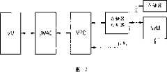
如图2中所说明的,如果在同一存储总线上没有附加其他任何协议,而需要对其他的存储器装置进行控制,则MPC也可以与传统存储器控制器一起使用。外部部件可以共用数据线、地址线和控制信号。如图2中所说明的,专用NVM控制线可以直接连到MPC。As illustrated in Figure 2, the MPC can also be used with conventional memory controllers if there are no other protocols attached to the same memory bus that require control of other memory devices. External components can share data lines, address lines, and control signals. As illustrated in Figure 2, dedicated NVM control lines can be connected directly to the MPC.
在下文中,将参考图3至22具体说明图2中所示的该装置的一个特殊示范实施例。图3用示意图示出了NAND闪存的写操作的数据流,并且图4用示意图示出了NAND闪存的读操作的数据流。图2中的存储器协议控制器(MPC)在图3和4中注解为“闪存控制DMA端口”。FCDP允许闪存装置(NAND闪存和NOR闪存)和RAM之间的独立数据块的传输,这样CPU负荷和片上总线通信量将保持在最小。图3和4中的闪存控制器对应于图2中的传统存储器控制器。Hereinafter, a specific exemplary embodiment of the device shown in FIG. 2 will be described in detail with reference to FIGS. 3 to 22 . FIG. 3 schematically shows a data flow of a write operation of a NAND flash memory, and FIG. 4 schematically shows a data flow of a read operation of a NAND flash memory. The Memory Protocol Controller (MPC) in Figure 2 is annotated "Flash Control DMA Port" in Figures 3 and 4. FCDP allows the transfer of individual blocks of data between flash devices (NAND flash and NOR flash) and RAM so that CPU load and on-chip bus traffic are kept to a minimum. The flash memory controller in FIGS. 3 and 4 corresponds to the conventional memory controller in FIG. 2 .
为了减小CPU负荷,在初始化配置处理之后,与DMAC相结合的FCDP在没有进一步支持的条件下能够传送任何需要的数据量(也就是说在NAND闪存的情况下为页)。In order to reduce the CPU load, after the initial configuration process, FCDP in combination with the DMAC is able to transfer any required amount of data (that is to say pages in the case of NAND flash) without further support.
此外,FCDP产生用于向NAND闪存装置进行写入操作的错误校正代码(ECC),以及用于从NAND闪存装置进行读出操作的错误校正代码的检测。对NOR闪存装置的读访问通过可配置地址产生器的提供来加速。In addition, the FCDP generates error correction code (ECC) for a write operation to the NAND flash memory device, and detection of the error correction code for a read operation from the NAND flash memory device. Read access to NOR flash devices is accelerated by the provision of configurable address generators.
为了减少总线数据通信量,使用内部FIFO,FCDP支持四个传输(32位)的脉冲串传送。To reduce bus data traffic, FCDP supports burst transfers of four transfers (32 bits) using internal FIFOs.
为了使得连接闪存和产生装置特定时间匹配成为可能,FCDP需要一个外部存储器控制器或闪存控制器。图5示出了FCDP的结构示意图,在这种情况下FCDP被解释为处于非常高的电平,也就是说再分成更加低级的块。To make it possible to connect flash memory and generate device-specific time matching, FCDP requires an external memory controller or flash controller. Fig. 5 shows a schematic diagram of the structure of the FCDP, which in this case is interpreted at a very high level, that is to say subdivided into even lower-level blocks.
图5中的FCDP解释为The FCDP in Figure 5 is interpreted as
-同步操作,- synchronous operation,
-具有单独的块(AHB块/AHB=先进高性能总线=现代高性能总线),- have a separate block (AHB block / AHB = Advanced High Performance Bus = Modern High Performance Bus),
-符合AMBA AHB2.0规范(“AMBA”是先进RISC机器有限公司/ARM Ltd的商标并且事实上表示片上总线的标准),- conforms to the AMBA AHB2.0 specification ("AMBA" is a trademark of Advanced RISC Machines Limited/ARM Ltd and de facto denotes the standard for the on-chip bus),
-具有带有AHB莱特(lite)接口的AHB主设备,- has an AHB master with an AHB lite interface,
-具有用于ARM主单元DMAC的接口,- has an interface for the ARM main unit DMAC,
-通过硬件ECC支持NAND闪存读/写,- Support NAND flash read/write via hardware ECC,
-支持NOR闪存读传输,并且-Supports NOR flash read transfers, and
-支持脉冲串模式的读/写传输。- Supports read/write transfers in burst mode.
为了能够获得FCDP的支持,NAND闪存装置必须满足下列要求:In order to be supported by FCDP, a NAND flash device must meet the following requirements:
-支持“CE无关”模式,- Support "CE independent" mode,
-仅在地址或命令周期之后操作“占用/就绪”输出,- the Occupy/Ready output is manipulated only after an address or command cycle,
-列地址包括两个以上地址字节,- the column address consists of two or more address bytes,
-行地址包括四个以上地址字节,- the row address consists of four or more address bytes,
-ECC产生/检测:-ECC generation/detection:
-主区域:超过2048字节- Main area: more than 2048 bytes
-备用区域:超过32字节- Spare area: more than 32 bytes
-页大小(如果不受ECC的块大小的限制):超过4096字节。- Page size (if not limited by ECC's block size): more than 4096 bytes.
AHB从接口执行下列任务:The AHB slave interface performs the following tasks:
-从RAM到FCDP的数据传输(闪存写访问),- data transfer from RAM to FCDP (flash write access),
-从FCDP到RAM的数据传输(闪存读访问),- data transfer from FCDP to RAM (flash read access),
-FCDP配置接口,- FCDP configuration interface,
-FCDP命令接口。- FCDP command interface.
在很多情况下,虽然使用DMA(直接存储器存取)处理数据传输,如果需要,也就是说如果可用的DMA信道是不足的,其也可以通过CPU在中断驱动基线上执行数据传输。In many cases, although data transfers are handled using DMA (Direct Memory Access), it is also possible to perform data transfers on an interrupt-driven basis by the CPU if required, that is, if the available DMA channels are insufficient.
配置接口允许对FCDP控制/状态寄存器的访问。寄存器接口允许被配置成通用操作模式,此模式用于相对大数量的交易,也就是说该交易对现有闪存装置、总线结构、DMA配置、存储器映射等是特殊的。The configuration interface allows access to the FCDP control/status registers. The register interface allows to be configured in a generic mode of operation, which is used for a relatively large number of transactions, that is to say the transactions are specific to existing flash devices, bus structures, DMA configurations, memory maps, etc.
命令接口用作对FCDP执行的控制传输的目的。许多命令也需要特殊的参数。命令接口能够通过DMA被访问,也就是说当前一页已经被完全作用完时,下一页的复制就被触发。The command interface is used for the purpose of control transfers to FCDP execution. Many commands also require special parameters. The command interface can be accessed via DMA, which means that when the previous page has been fully utilized, the copying of the next page is triggered.
AHB主设备接口处理传送到外部存储器接口/来自外部存储器接口的传输。取决于如何设置整个系统,可以将其设计成既可以使用为最优化利用带宽的脉冲串传输,也可以使用为减小AHB上判断延迟的单独传输。为了允许有效地使用脉冲串传输,外部存储器接口应当能够缓冲一定量的数据。The AHB master interface handles transfers to/from the external memory interface. Depending on how the overall system is set up, it can be designed to use either burst transfers for optimal utilization of bandwidth, or individual transfers to reduce decision delays on the AHB. To allow efficient use of burst transfers, the external memory interface should be able to buffer a certain amount of data.
FCDP也可以具有FIFO以允许当一侧在处理其他事务时,在另一侧保持传输,例如当总线访问许可未授权或DMA信道未就绪时。当需要时,FIFO同样允许在一个AHB接口上使用脉冲串传输并且在其他AHB接口上使用单独传输。FCDP can also have FIFOs to allow transmissions to be held on the other side while one side is doing other things, such as when bus access permission is not granted or a DMA channel is not ready. The FIFO also allows the use of burst transfers on one AHB interface and individual transfers on the other AHB interface when required.
FCDP实质上使用组合的传输/接收FIFO(TX/RX FIFO),此FIFO是基于上旋(topspin)外围体系结构概念。然而,由于FCDP的特殊需要,存在几处较小的不同和特定特征:FCDP essentially uses a combined transmit/receive FIFO (TX/RX FIFO), which is based on the topspin peripheral architectural concept. However, due to the specific needs of FCDP, there are several minor differences and specific features:
-在FCDP_FIFO_CFG寄存器中不存在“最大接收包大小”的字段,由于FCDP不需要处理任何未请求的传输,也就是说包大小仅通过命令字来限定。- There is no "maximum received packet size" field in the FCDP_FIFO_CFG register, because FCDP does not need to process any unsolicited transfers, that is to say, the packet size is only limited by the command word.
-由于读取和写入交易的包大小由写入FCDP_COMMAND寄存器的命令字来限定,所以既没有“接收包大小”寄存器(RPS_STAT),也没有“传输包大小”寄存器(TPS_CTRL)。- Since the packet size for read and write transactions is defined by the command word written to the FCDP_COMMAND register, there is neither a "Receive Packet Size" register (RPS_STAT) nor a "Transmit Packet Size" register (TPS_CTRL).
-FIFO总是利用字对齐来进行操作。-FIFOs always operate with word alignment.
-在“接收状态”和“发送状态”之间的切换由写入到FCDP_COMMAND寄存器的命令字来控制。- Switching between "receive state" and "transmit state" is controlled by the command word written to the FCDP_COMMAND register.
-FCDP总是流控制器,对于DMA传输,也就是序列控制器。- FCDP is always the flow controller, and for DMA transfers, the sequence controller.
在此,在说明示范实施例的情况下,FIFO的大小是8×32位。Here, in the case of explaining the exemplary embodiment, the size of the FIFO is 8*32 bits.
为了检测NAND闪存装置的位错误并在可能时校正它们,FCDP提供了错误校正代码(ECC)产生和检测机制。ECC算法为汉明码,其允许单个位错误的校正和在一页中超过两位错误的校正。In order to detect bit errors of NAND flash memory devices and correct them when possible, FCDP provides an error correction code (ECC) generation and detection mechanism. The ECC algorithm is a Hamming code, which allows correction of single bit errors and correction of more than two bit errors in a page.
用于闪存页的主区域中的ECC存储在同一页的备用区域中。在相同的方式,备用区域由第二个ECC进行错误检测,第二ECC同样存储在备用区域中。The ECC used in the main area of a flash page is stored in the spare area of the same page. In the same way, the spare area is subjected to error detection by the second ECC, which is also stored in the spare area.
一旦提供一个合适的启动,ECC就由FCDP产生并且在写访问中被写入到闪存,达到此目的不需要任何CPU的辅助。在读访问中,ECC由从闪存中获得的数据产生并且与存储在闪存中的ECC进行比较。如果发现不匹配,那么将一个错误中断传给CPU,并且停止进一步的交易。这使得CPU可能检测错误是否被校正,并且,如果可能,校正此错误。Once a suitable boot is provided, ECC is generated by FCDP and written to flash memory on a write access, without any CPU assistance for this purpose. In a read access, the ECC is generated from the data obtained from the flash memory and compared with the ECC stored in the flash memory. If a mismatch is found, an error interrupt is passed to the CPU and further transactions are stopped. This makes it possible for the CPU to detect whether an error has been corrected, and, if possible, correct the error.
主区域和备用区域ECC的产生和检测能够彼此相互独立地被激活或撤销。为了允许闪存文件系统能够经常地更换一些信息项,备用区域中的一些位将被排除在ECC结果之外。The generation and detection of the main area and the backup area ECC can be activated or deactivated independently of each other. In order to allow the flash file system to frequently replace some information items, some bits in the spare area will be excluded from the ECC result.
主区域和备用区域ECC的存储器位置,以及一页中无保护部分的存储器位置是可配置的。The memory locations of the main area and the spare area ECC, and the memory locations of the unprotected part in one page are configurable.
使用一个二维等式检测作为ECC。在速度和区域方面此允许一个有效的硬件实现。Use a two-dimensional equation detection as ECC. This allows an efficient hardware implementation in terms of speed and area.
为了检测NAND闪存页中的数据还没有被破坏,存储在闪存中的ECC和当读数据时产生的ECC受到一个异或逻辑操作。这将导致下列情况之一:In order to detect that the data in the NAND flash page has not been corrupted, the ECC stored in the flash and the ECC generated when reading the data are subjected to an XOR logic operation. This will result in one of the following:
-所有位均为0:无错误- all bits are 0: no error
-每一奇偶校验位P<x>和其反码P<x>′彼此不相同(P<x><>P<x>′):可校正错误- Each parity bit P<x> and its inverse P<x>′ are different from each other (P<x><>P<x>′): correctable error
-仅有一位不为0:ECC中错误- only one bit is not 0: error in ECC
-其他情况(随机数据):不可校正错误- other cases (random data): uncorrectable errors
当一个错误发生时,FCDP给CPU产生一个错误中断。然后,错误处理软件以适当的方式处理该错误。When an error occurs, FCDP generates an error interrupt to the CPU. The error handling software then handles the error in an appropriate manner.
如果发生可校正错误,ECC直接指出页中错误位的位置:P8192、P4096、P2048、……、P16:位错误P8、P4、P2、P1的16位字地址:错误的位的位置。If a correctable error occurs, ECC directly points out the position of the wrong bit in the page: P8192, P4096, P2048, ..., P16: 16-bit word address of bit error P8, P4, P2, P1: the position of the wrong bit.
外部存储接口被用于连接闪存装置。The external storage interface is used to connect the flash memory device.
为了与NAND闪存装置相互作用,外部存储器控制器在异步模式下工作。如图6所示,相应于外部16位字地址A(16)和A(17)的内部位地址A(17)和A(18)上两个地址输出线被用于控制NAND闪存输入信号ALE(地址锁存使能)和CLE(命令锁存使能)。In order to interact with the NAND flash memory device, the external memory controller works in asynchronous mode. As shown in Figure 6, the two address output lines on the internal bit addresses A(17) and A(18) corresponding to the external 16-bit word addresses A(16) and A(17) are used to control the NAND flash memory input signal ALE (Address Latch Enable) and CLE (Command Latch Enable).
NAND闪存输出信号R/B仅被FCDP处理。只有在处理执行时间相对较长的命令(读取页、写入页、删除页)时,其被闪存装置设置为低电平。The NAND flash output signal R/B is only processed by FCDP. It is set low by the flash memory device only when processing commands with a relatively long execution time (read page, write page, delete page).
通过同步或异步NOR闪存接口对装置的读访问,需要具有与AHB从端口相配合的存储器控制器。由于AHB总线上的INCR4请求能够由来自闪存装置的脉冲串传输进行处理(INCR4为通常已被接受的,根据AHB规范中特殊脉冲串请求的缩写,其中脉冲串宽度为增量的/INCR/,也就是说已增加的),连接到同步脉冲串NOR闪存的同步脉冲串模式控制器获得较好的传输速度。Read access to the device via a synchronous or asynchronous NOR flash interface requires a memory controller with an AHB slave port. Since the INCR4 request on the AHB bus can be processed by a burst transfer from the flash memory device (INCR4 is generally accepted, according to the abbreviation of the special burst request in the AHB specification, where the burst width is incremented /INCR/, That is to say has been increased), the synchronous burst mode controller connected to the synchronous burst NOR flash memory obtains better transmission speed.
NAND闪存装置和NOR闪存装置通常均具有写保护( WP-写保护)输入。此输入不通过FCDP控制但必须根据装置规范来处理,例如通过将其连接到GPIO(通用输入/输出)或接通复位信号。Both NAND flash memory devices and NOR flash memory devices are usually write-protected ( WP-Write Protect) input. This input is not controlled via FCDP but must be handled according to the device specification, for example by connecting it to a GPIO (General Purpose Input/Output) or switching on a reset signal.
通过将一个命令写入到FCDP命令寄存器,从而初始化每个FCDP处理。此通常是通过在RAM中产生一个命令序列并使DMA控制器根据请求准备将命令写入到FCDP来完成的。第一命令请求由软件通过设定DMA命令请求位来触发。一旦前一个命令执行完毕,FCDP将请求其后的每一个命令。STOP命令用于阻止FCDP请求进一步的命令。Each FCDP transaction is initiated by writing a command to the FCDP Command Register. This is usually done by generating a sequence of commands in RAM and having the DMA controller prepare the commands to be written to the FCDP upon request. The first command request is triggered by software by setting the DMA command request bit. Once the previous command has been executed, FCDP will request each subsequent command. The STOP command is used to prevent FCDP from requesting further commands.
表1提供了FCDP命令的综述。如同所看到的,一些命令需要附加的参数。虽然大部分命令以单个32位字的形式存在,但也一部分命令需要第二个32位字以允许32位地址参数的加密。Table 1 provides an overview of FCDP commands. As you can see, some commands require additional parameters. While most commands exist as a single 32-bit word, some commands require a second 32-bit word to allow encryption of 32-bit address parameters.
表1:FCDP命令综述
下面,表2示出了FCDP寄存器接口的综述。Below, Table 2 shows an overview of the FCDP register interface.
表2:寄存器编程接口
FCDP产生两种类型的DMA请求,特定的数据请求和命令请求。这为设置DMAC的链接表的创建提供了特别的简化。FCDP generates two types of DMA requests, specific data requests and command requests. This provides particular simplification for the creation of linked lists for setting up the DMAC.
只要FCDP命令执行完毕,即产生一个DMA命令请求,并且必须将一个新的命令写入FCDP命令寄存器。该DMA命令请求始终是一个单个的DMA请求。As soon as the FCDP command is executed, a DMA command request is generated and a new command must be written into the FCDP command register. The DMA command request is always a single DMA request.
在闪存读取操作期间FIFO中有足够的数据时,或者在闪存写操作期间FIFO中有足够的空间时,就产生DMA数据请求。所有的传输除最后一个之外均在DMA脉冲串请求中结束,最后一个同样由FCDP命令的传输数量参数确定。最后的传输结束于DMA“最后脉冲串”请求,此请求发送给DMAC,且其必须变成链接表中的下一个条目。A DMA data request is generated when there is enough data in the FIFO during a flash read operation, or when there is enough space in the FIFO during a flash write operation. All transfers except the last one end in a DMA burst request, which is also determined by the number of transfers parameter of the FCDP command. The last transfer ends with a DMA "last burst" request, which is sent to the DMAC and which must become the next entry in the linked table.
如果没有足够多的DMA信道可用,取而代之,使用数据请求中断、“最后数据请求”中断和命令请求中断也是可能的。If not enough DMA channels are available, it is also possible to use the data request interrupt, "last data request" interrupt and command request interrupt instead.
在下文中将对各种中断请求进行更加详细的描述。Various interrupt requests will be described in more detail below.
-命令请求中断(CMD)- Command Request Interrupt (CMD)
命令请求中断的调用向FCDP表明下一命令能够被写入到命令寄存器(FCDP_COMMAND)并且表明以前命令的执行已经全部完成。命令请求中断能够被用于代替DMA命令请求。A command request interrupt call indicates to FCDP that the next command can be written to the command register (FCDP_COMMAND) and that execution of previous commands has been fully completed. A command request interrupt can be used instead of a DMA command request.
-数据脉冲串请求中断(DAT)- Data burst request interrupt (DAT)
根据现在正在执行的是哪个命令,FCDP输出数据脉冲串请求中断以表明数据必须被写入到写缓冲寄存器(FCDP_WRBUF)中或者表明数据必须被从读缓冲寄存器(FCDP_RDBUF)中读出。脉冲串的大小可以被编程为一个字或四个字。除了最后一个脉冲串之外,为在命令所定义的时序范围内的每个数据脉冲串输出数据脉冲串请求。该数据脉冲串请求中断能够用于取代DMA数据脉冲串请求。Depending on which command is currently executing, the FCDP output data burst requests an interrupt to indicate that data must be written into the write buffer register (FCDP_WRBUF) or that data must be read from the read buffer register (FCDP_RDBUF). The burst size can be programmed as one word or four words. A data burst request is output for every data burst within the timing range defined by the command except the last burst. The data burst request interrupt can be used in place of the DMA data burst request.
-“最后数据脉冲串”请求中断(LDAT)- "Last data burst" request interrupt (LDAT)
“最后数据脉冲串”请求中断,其意义实质上与数据脉冲串请求中断相同。唯一的不同在于LDAT是仅为在命令所定义的时序范围内的最后一个脉冲串输出。LDAT能够用于取代DMA“最后脉冲串”请求。The "last data burst" request interrupt is essentially the same as the data burst request interrupt. The only difference is that LDAT is output only for the last burst within the timing range defined by the command. LDAT can be used to replace DMA "last burst" requests.
-主区域ECC错误中断(MECC)- Main area ECC error interrupt (MECC)
当发现从NAND闪存页中读取的ECC与从此页的主区域中读取数据所产生的ECC不匹配时,发生主区域ECC错误中断,并且在FCDP_NFECCCONFIG寄存器中激活主区域ECC检测。直到所有的传输已经完成并且所有的数据已经从FCDP_RDBUF寄存器中读取后,才内部复位主区域ECC错误中断。然后,FCDP等待刷新命令以确保已经与中断延迟无关地识别该错误。在接收到刷新命令后,FCDP通过请求下一个命令恢复到正常操作。When it is found that the ECC read from the NAND flash page does not match the ECC produced by reading data from the main area of this page, a main area ECC error interrupt occurs and the main area ECC detection is activated in the FCDP_NFECCCONFIG register. The main zone ECC error interrupt is not internally reset until all transfers have been completed and all data has been read from the FCDP_RDBUF register. FCDP then waits for a flush command to ensure that the error has been identified regardless of interrupt latency. After receiving a refresh command, FCDP resumes normal operation by requesting the next command.
-备用区域ECC错误中断(SECC)- Spare area ECC error interrupt (SECC)
当发现从NAND闪存页中读取的ECC与从该页的备用区域中读取数据所产生的ECC不匹配时,发生备用区域ECC错误中断,并且在FCDP_NFECCCONFIG寄存器中激活备用区域ECC检测。直到所有的传输已经完成并且所有的数据已经从FCDP_RDBUF寄存器中读取后,才内部上推备用区域ECC错误中断。然后,FCDP等待刷新命令以确保已经与中断延迟无关地识别该错误。在接收到刷新命令后,FCDP通过请求下一个命令恢复到正常操作。When it is found that the ECC read from a NAND flash page does not match the ECC produced by reading data from the spare area of that page, a spare area ECC error interrupt occurs and the spare area ECC detection is activated in the FCDP_NFECCCONFIG register. The spare area ECC error interrupt is not pushed up internally until all transfers have been completed and all data has been read from the FCDP_RDBUF register. FCDP then waits for a flush command to ensure that the error has been identified regardless of interrupt latency. After receiving a refresh command, FCDP resumes normal operation by requesting the next command.
-闪存状态错误中断(ST)- Flash status error interrupt (ST)
在执行NF_CHECK命令之后,当发现从NAND闪存装置读取的状态字节与NAND闪存状态比较寄存器(FCDP_NFCOMP)中定义的期望值不匹配时,发生闪存状态错误中断。比较是根据NAND闪存状态掩码寄存器(FCDP_NFMASK)来执行的。中断服务程序能够从NAND闪存状态寄存器(FCDP_NFSTATUS)中读取实际的状态字节。在闪存状态错误中断之后,FCDP等待刷新命令以确保已经与中断延迟无关地识别该错误。在接收到刷新命令后,FCDP通过请求下一个命令恢复到正常操作。After executing the NF_CHECK command, a flash status error interrupt occurs when it is found that the status byte read from the NAND flash device does not match the expected value defined in the NAND flash status comparison register (FCDP_NFCOMP). The comparison is performed against the NAND Flash Status Mask Register (FCDP_NFMASK). The interrupt service routine can read the actual status byte from the NAND flash status register (FCDP_NFSTATUS). After a flash status error interrupt, FCDP waits for a flush command to ensure that the error has been identified regardless of interrupt latency. After receiving a refresh command, FCDP resumes normal operation by requesting the next command.
-FIFO溢出/欠载错误中断(FIFO)- FIFO overflow/underrun error interrupt (FIFO)
在FIFO为空期间,当对读缓冲寄存器(FCDP_RDBUF)进行读访问时,或者在FIFO为满期间,当对写缓冲寄存器(FCDP_WRBUF)进行写访问时,则发生FIFO溢出/欠载错误中断。A FIFO overflow/underrun error interrupt occurs when a read access is made to the read buffer register (FCDP_RDBUF) while the FIFO is empty, or when a write access is made to the write buffer register (FCDP_WRBUF) while the FIFO is full.
-保护错误中断(PE)- Protection Fault Interrupt (PE)
保护错误中断在下列情况下发生:A protection fault interrupt occurs when:
-一个已经在NAND闪存“保护命令”寄存器(FCDP_NFPROTCMD)中被指定受保护的命令,在一个在NAND闪存地址窗口寄存器(FCDP_NFADDRWIN1L、FCDP_NFADDRWIN2L)中被指定的受保护NAND闪存地址区域(页)中输出。在NAND闪存处理期间的保护错误中断之后(也就是说不是在保护寄存器FCDP_NFPASSW、FCDP_NFPROTCMD、FCDP_NFADDRWIN1L和FCDP_NFADDRWIN1H配置期间,FCDP_MODE.RUN=“0”),FCDP等待刷新命令以确保已经与中断延迟无关地识别该错误。在接收到刷新命令后,FCDP通过请求下一个命令恢复到正常操作。- A command that has been designated as protected in the NAND Flash "Protection Command" register (FCDP_NFPROTCMD) is output in a protected NAND Flash address area (page) designated in the NAND Flash Address Window registers (FCDP_NFADDRWIN1L, FCDP_NFADDRWIN2L) . After a protection fault interrupt during NAND flash processing (i.e. not during configuration of the protection registers FCDP_NFPASSW, FCDP_NFPROTCMD, FCDP_NFADDRWIN1L and FCDP_NFADDRWIN1H, FCDP_MODE.RUN="0"), FCDP waits for a refresh command to ensure that it has been recognized independently of the interrupt latency The error. After receiving a refresh command, FCDP resumes normal operation by requesting the next command.
-通过将校正密码写入到NAND闪存密码寄存器(FCDP_NFPASSWD)中,没有首先打开NAND闪存“保护命令”寄存器(FCDP_NFPROTCMD),NAND闪存“保护命令”寄存器就被写入。- By writing the correction password into the NAND Flash Password Register (FCDP_NFPASSWD), the NAND Flash "Protection Command" Register (FCDP_NFPROTCMD) is written without first opening the NAND Flash "Protection Command" Register (FCDP_NFPROTCMD).
-通过将校正密码写入到NAND闪存密码寄存器(FCDP_NFPASSWD)中,没有首先打开NAND闪存地址窗口1寄存器(FCDP_NFADDRWIN1L),NAND闪存地址窗口1寄存器就被写入。- By writing the calibration password into the NAND Flash Password Register (FCDP_NFPASSWD), the NAND
-一个错误的密码已经被写入NAND闪存密码寄存器(FCDP_NFPASSWD)。- A wrong password has been written to the NAND flash password register (FCDP_NFPASSWD).
-命令错误中断(CE)- Command Error Interrupt (CE)
当未定义命令被写入到命令寄存器FCDP_COMMAND中时,产生命令错误中断。在命令错误中断之后,FCDP等待刷新命令以确保已经与中断延迟无关地识别该错误。在接收到刷新命令后,FCDP通过请求下一个命令恢复到正常操作。When an undefined command is written into the command register FCDP_COMMAND, a command error interrupt is generated. After a command error interrupt, FCDP waits for a flush command to ensure that the error has been identified regardless of the interrupt delay. After receiving a refresh command, FCDP resumes normal operation by requesting the next command.
-命令溢出错误中断(CO)- Command overflow error interrupt (CO)
当在前一命令被完全处理之前将命令写入到命令寄存器FCDP_COMMAND时,也就是说下一命令还没有被请求时,产生命令溢出错误中断。A command overflow error interrupt is generated when a command is written to the command register FCDP_COMMAND before the previous command has been completely processed, that is, when the next command has not been requested.
-AHB错误中断(AE)-AHB error interrupt (AE)
当FCDP中的AHB主接口检测到AHB错误响应时,产生AHB错误中断。该AHB错误的原因必须通过AHB从模块指示给该接口。一旦产生AHB错误中断,命令执行将立即终止,并且FCDP等待刷新命令以确保已经与中断延迟无关地识别该错误。在接收到刷新命令后,FCDP通过请求下一个命令恢复到正常操作。When the AHB master interface in FCDP detects an AHB error response, an AHB error interrupt is generated. The cause of this AHB error must be indicated to this interface by the AHB slave module. Once an AHB error interrupt is generated, command execution is terminated immediately and FCDP waits for a flush command to ensure that the error has been identified regardless of interrupt latency. After receiving a refresh command, FCDP resumes normal operation by requesting the next command.
NAND闪存装置的基址在FCDP配置寄存器中被指定。AHB主接口为NAND闪存装置仅产生三个不同的地址,这三个不同的地址取决于访问类型:The base address of the NAND flash device is specified in the FCDP configuration register. The AHB master interface generates only three different addresses for the NAND flash device, which depend on the type of access:
-<基址>:数据-<base address>: data
-<基址>+0×20000:地址-<base address>+0×20000: address
-<基址>+0×40000:命令-<base address>+0×40000: command
当通过NF_WR命令或NF_RD命令选择INCR4脉冲串传输时,根据AHB规范产生地址。When the INCR4 burst transmission is selected by the NF_WR command or the NF_RD command, the address is generated according to the AHB specification.
NAND闪存页地址和NAND闪存行地址是FCDP命令序列的一部分,并且它们与AHB地址产生无关。NAND Flash Page Address and NAND Flash Row Address are part of the FCDP command sequence, and they are independent of AHB address generation.
对于NOR闪存装置,FCDP为每个读访问产生地址和AHB传输类型(时序的或非时序的):<开始>、<开始>+0×04、<开始>+0×08、<开始>+0×0C、……,<开始>表示传输的序列的初始起始地址。根据AHB规范中所定义的,必须要记住的是,<开始>必须要对准字地址的边界并且脉冲串一定不能超过边界1KB。For NOR flash devices, FCDP generates address and AHB transfer type (sequential or non-sequential) for each read access: <start>, <start>+0×04, <start>+0×08, <start>+ 0×0C, ..., <start> indicates the initial starting address of the transmitted sequence. As defined in the AHB specification, it must be remembered that <start> must be aligned on a word address boundary and the burst must not exceed the boundary by 1KB.
初始起始地址和将要被执行的脉冲串的数量是FCDP命令序列的一部分。The initial starting address and the number of bursts to be executed are part of the FCDP command sequence.
脉冲串模式写命令与脉冲串模式读命令以相同的方式工作。The burst mode write command works in the same way as the burst mode read command.
硬件保护机构防止无意的或未经许可的NAND闪存删除和写操作。A hardware protection mechanism prevents inadvertent or unauthorized NAND flash memory deletion and write operations.
FCDP将写命令和读命令的地址与可用于写的地址区域进行比较。如果地址不在所允许的地址区域内,则FCDP取消到闪存装置的那些命令的输出并且产生错误中断。FCDP compares the addresses of write commands and read commands with the address area available for writing. If the address is not within the allowed address region, FCDP cancels the output of those commands to the flash device and generates an error interrupt.
在页基础上执行保护。保护解锁寄存器的内容指定页地址区域。涉及写和删除保护功能的一套NAND闪存命令必须由软件来定义,例如块删除(D0h)和页编程(10h)。如果所指定的页地址没有位于可容许的地址区域(地址窗口)内并且随后的命令指定为保护命令,则产生保护命令中断,并且关键命令将不被送入NAND闪存。Protection is performed on a page basis. The content of the protection unlock register specifies the page address area. A set of NAND flash commands related to write and erase protection functions must be defined by software, such as block delete (D0h) and page program (10h). If the specified page address is not within the allowable address area (address window) and the subsequent command is specified as a protection command, a protection command interrupt is generated and critical commands will not be sent to the NAND flash memory.
如图7中所示,执行写保护的两个电平N1、N2。只有那些在两个电平N1、N2中均开放的地址区域能被用作写和删除操作。在复位之后,两个锁定处理覆盖了所有地址区域。As shown in FIG. 7, two levels N1, N2 of write protection are performed. Only those address areas that are open in both levels N1, N2 can be used for write and delete operations. After reset, two lock processes cover all address areas.
第一电平地址窗口寄存器的设定允许地址区域的一部分用作写和删除操作。此第一保护电平N1保护例如用于移动电话的程序和主功能,以防止被改写。The setting of the first level address window register allows a part of the address area to be used for write and delete operations. This first protection level N1 protects, for example, programs and main functions of a mobile phone against being overwritten.
在类似的寄存器中指定第二保护电平N2。其可以用作单独的驱动器,例如用于闪存文件系统。The second protection level N2 is specified in a similar register. It can be used as a separate drive, for example for flash file systems.
保护命令设置寄存器和第一电平地址窗口寄存器由密码机构保护。The protection command setting register and the first level address window register are protected by a cryptographic mechanism.
为了减少动态功率损耗,FCDP提供四种不同操作模式,具体而言:To reduce dynamic power loss, FCDP offers four different modes of operation, specifically:
-睡眠:FCDP_CLC寄存器中的外设时钟已经被切断。在此模式下,仅对寄存器的读访问是可能的。- Sleep: Peripheral clock in FCDP_CLC register has been cut off. In this mode, only read access to registers is possible.
-配置:FCDP_CLC寄存器中的外设时钟已经被接通,并且运行模式被去激活(FCDP_MODE.RUN=“0”)。在此模式下,除了FCDP_COMMAND之外,对所有的寄存器都是能进行写访问。大部分外设内核的时钟是无效的。- Configuration: the peripheral clock in the FCDP_CLC register has been switched on and the run mode is deactivated (FCDP_MODE.RUN="0"). In this mode, except for FCDP_COMMAND, all registers are write-accessible. Most of the peripheral core clocks are invalid.
-仅NOR闪存模式操作:FCDP_CLC寄存器中的外设时钟已接通、运行模式使能(FCDP_MODE.RUN=“1”)并且NAND闪存操作被切断(FCDP_MODE.NFEN=“0”)。在此模式下,对配置寄存器的写访问是不可能的。除了NAND闪存命令之外的FCDP命令能被写入到FCDP_COMMAND寄存器中。内核的NAND闪存特殊部分的时钟被切断。- NOR flash mode operation only: peripheral clock in FCDP_CLC register is on, run mode is enabled (FCDP_MODE.RUN = "1") and NAND flash operation is switched off (FCDP_MODE.NFEN = "0"). In this mode, write access to configuration registers is not possible. FCDP commands other than NAND flash commands can be written into the FCDP_COMMAND register. The clock to the NAND flash special part of the core is cut off.
-完全操作:FCDP_CLC寄存器中的外设时钟已接通、运行模式被激活(FCDP_MODE.RUN=“1”)并且NAND闪存操作被启动(FCDP_MODE.NFEN=“1”)。在此模式下,对配置寄存器的写访问是可能的。所有FCDP命令包括NAND闪存命令能被写入到FCDP_COMMAND寄存器。- Full operation: Peripheral clocks in FCDP_CLC registers are on, run mode is activated (FCDP_MODE.RUN="1") and NAND flash operation is started (FCDP_MODE.NFEN="1"). In this mode, write access to configuration registers is possible. All FCDP commands including NAND flash commands can be written to the FCDP_COMMAND register.
最后,在描述的示范实施例中的接口将在下文中更详细地说明。Finally, the interfaces in the described exemplary embodiment will be explained in more detail below.
AHB从接口AHB slave interface
-支持传输尺寸:32位-Support transfer size: 32 bits
-支持脉冲串尺寸:单个、INCR4(FIFO只读/写)-Support burst size: single, INCR4 (FIFO read/write only)
-支持传输响应:对、错。- Support transport response: true, false.
AHB主接口AHB main interface
-支持传输尺寸:32位(对于某些NAND闪存访问+16位)- Support transfer size: 32 bits (+16 bits for some NAND flash access)
-支持脉冲串尺寸:单个、INCR4-Supported burst size: single, INCR4
-AHB莱特接口-AHB Wright interface
DMAC接口DMAC interface
-支持对数据的脉冲串请求和“最后脉冲串”请求- Support for burst requests and "last burst" requests for data
-单个传输能够以同脉冲串传输一样的方式由DMAC处理- A single transfer can be handled by the DMAC in the same way as a burst transfer
-支持对命令的单个请求-Supports a single request for a command
-需要两个独立的用于数据和命令的DMA信道- Requires two separate DMA channels for data and commands
-所有DMA请求能够象中断一样随意被处理- All DMA requests can be handled as interrupts at will
NAND闪存接口NAND flash interface
nand_flash_busy_n_i:链接到闪存装置的Ready/Busy_N输出。此信号完全地异步处理。nand_flash_busy_n_i: Links to the Ready/Busy_N output of the flash device. This signal is handled completely asynchronously.
调试接口debug interface
调试接口允许FCDP的某些内部信号被监控。在装置的监控插脚上对存取有用的这些信号在表3中列出。The debug interface allows certain internal signals of FCDP to be monitored. The signals available for access on the monitor pins of the device are listed in Table 3.
表3:监控信号
在下文中,我们将转为对NAND闪存ECC寄存器的更加全面的描述。In the following, we turn to a more comprehensive description of the NAND flash ECC registers.
FCDP_NFECCCONFIG寄存器可以指定是否通过NF_WR命令将主区域ECC和备用区域ECC写入NAND闪存,以及是否通过NF_RD命令对它们进行检测。主尺寸(MAINSIZE)字段定义了一页的主区域的大小,该页必须是2的幂(32位字)。The FCDP_NFECCCONFIG register can specify whether to write the main area ECC and spare area ECC to the NAND flash memory through the NF_WR command, and whether to detect them through the NF_RD command. The main size (MAINSIZE) field defines the size of the main area of a page, which must be a power of 2 (32-bit words).
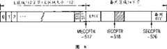
FCDP_NFMECCPTR和FCDP_NFSECCPTR寄存器表示一页中的主区域ECC和备用区域ECC的存储位置。The FCDP_NFMECCPTR and FCDP_NFSECCPTR registers indicate the storage locations of the main area ECC and the spare area ECC in one page.
用于ECC产生/检测的备用区域在由FCDP_NFECCCONFIG.MAINSIZE定义的主区域之后立即开始,并且结束于由FCDP_NFSECCPTR定义的位置。必须使用软件来保证此区域不超过32字节(见图9)。The spare area for ECC generation/detection starts immediately after the main area defined by FCDP_NFECCCONFIG.MAINSIZE and ends at the location defined by FCDP_NFSECCPTR. Software must be used to ensure that this area does not exceed 32 bytes (see Figure 9).
FCDP_NFIECCPTR寄存器定义在一页的备用区域中的16位字,该16位字不包括在ECC产生中。在示范实施例中,其中是不需要该特征的,FCDP_NFIECCPTR能被设定为在有效页尺寸之外的值。The FCDP_NFIECCPTR register defines a 16-bit word in the spare area of a page, which is not included in ECC generation. In an exemplary embodiment, where this feature is not required, FCDP_NFIECCPTR can be set to a value outside the valid page size.
当FCDP_NFSECCPTR和FCDP_NFIECCPTR必须和一个16位边界对准时,FCDP_NFMECCPTR必须和一个32位地址边界对准。While FCDP_NFSECCPTR and FCDP_NFIECCPTR must be aligned to a 16-bit boundary, FCDP_NFMECCPTR must be aligned to a 32-bit address boundary.
必须要记住的是,备用区域ECC必须跟随其要保护的备用区域的一部分。It must be remembered that the spare area ECC must follow the part of the spare area it is intended to protect.
图8示出了页配置的一个实施例。阴影部分不包括在备用区域ECC计算中。Figure 8 shows one embodiment of a page configuration. Shaded areas are not included in the spare area ECC calculation.
FCDP_NFMECCST和FCDP_NFSECCST寄存器各自表示主区域ECC和备用区域ECC。一旦写命令(NF_WR)已经被完全执行,则两个寄存器显示从写入页数据中计算出的ECC。一旦读命令(NF_RD)已经被完全执行,则两个寄存器显示ECC的结果,该ECC是由具有读ECC的读数据通过异或连接计算得到的。The FCDP_NFMECCST and FCDP_NFSECCST registers represent the main area ECC and the spare area ECC, respectively. Once the write command (NF_WR) has been fully executed, two registers show the ECC calculated from the written page data. Once the read command (NF_RD) has been fully executed, the two registers show the result of the ECC calculated from the read data with read ECC by exclusive OR connection.
如果检测启动并且结果不等于零,就产生相关联的ECC错误中断。此时,软件能够读取ECC状态寄存器以确定错误类型并初始化进一步的测量。ECC状态寄存器的配置可以检测其是否是可校正的错误(P<8192..P1>XORP<8192..P1>′),并且允许位错误的位置被有效读取。If the test is enabled and the result is not equal to zero, an associated ECC error interrupt is generated. At this point, software can read the ECC status register to determine the type of error and initiate further measurements. The configuration of the ECC status register can detect whether it is a correctable error (P<8192..P1>XORP<8192..P1>'), and allows the position of the bit error to be effectively read.
在ECC错误中断结束之后,必须将刷新命令写入命令寄存器,确认该错误。After the end of the ECC error interrupt, a refresh command must be written to the command register to acknowledge the error.
下列表4到9应该和附图10到15被一起阅读(表4-图10、表5-图11、表6-图12、等等)。上述最后提及的多个表和多个附图提供了NAND闪存ECC寄存器的可视化的说明。Tables 4 to 9 below should be read together with Figures 10 to 15 (Table 4-10, Table 5-11, Table 6-12, etc.). The above last mentioned tables and figures provide a visual illustration of the NAND flash ECC registers.
表4
表5
表6
表7
表8
表9
参考图16到22,在下文中将更加具体地说明保护寄存器。Referring to FIGS. 16 to 22, the protection register will be described in more detail hereinafter.
图16用图解法示出了保护机构。当指定的NAND闪存行地址(页/块地址)没有位于由NAND闪存地址窗口寄存器(FCDP_NFADDRWIN1L、FCDP_NFADDRWIN1H、FCDP_NFADDRWIN2L和FCDP_NFADDRWIN2H)指定的地址区域中时,那么下列NAND闪存命令与存储在FCDP_NFPROTCMD寄存器中的保护命令列表CMD0……3进行比较。如果发现匹配,则输出保护错误中断,FCDP就停止。否则,NAND闪存命令有效,并且传送到闪存装置(见图7)。Figure 16 shows the protective mechanism diagrammatically. When the specified NAND Flash row address (page/block address) is not located in the address area specified by the NAND Flash Address Window Registers (FCDP_NFADDRWIN1L, FCDP_NFADDRWIN1H, FCDP_NFADDRWIN2L, and FCDP_NFADDRWIN2H), then the following NAND Flash Command list CMD0...3 for comparison. If a match is found, the output protection fault interrupts and FCDP stops. Otherwise, the NAND flash command is valid and sent to the flash device (see Figure 7).
在NF_ADDR命令执行期间,在内部接收NAND闪存行地址。在所有的随后的NF_CMD命令期间,保护机构使用该行地址,直到其他NF_ADDR命令指定新的行地址。因此,为保证保护机构的正确操作,在FCDP_NFPROTCMD寄存器中应该指定第二NAND闪存命令字节(两字节命令周期)。The NAND flash row address is received internally during NF_ADDR command execution. The protection mechanism uses this row address during all subsequent NF_CMD commands until other NF_ADDR commands specify a new row address. Therefore, to ensure correct operation of the protection mechanism, the second NAND flash command byte (two-byte command period) should be specified in the FCDP_NFPROTCMD register.
存在两种可能的方式来切断保护机构:There are two possible ways to switch off the protection mechanism:
1.仅遮蔽在FCDP_NFPROTCMD寄存器中指定的命令(也就是说对NAND闪存装置正在使用无效的命令字节)。1. Only mask commands specified in the FCDP_NFPROTCMD register (that is to say invalid command bytes are being used for NAND flash devices).
2.配置地址窗口寄存器以使其包括全部NAND闪存行地址区域。2. Configure the address window register to include the entire NAND Flash row address region.
CMD1“受保护命令”寄存器和用于第一保护电平N1的地址窗口寄存器(FCDP_NFADDRWIN1L和FCDP_NFADDRWIN1H)均由FCDP_NFPASSWD密码寄存器保护。该密码必须由在复位之后的对该寄存器进行的第一写访问所定义。每个具有相同密码的随后的写访问打开受保护的寄存器用于进行一次并且仅一次写访问。密码寄存器的内容是不能被读取的。The CMD1 "command protected" register and the address window registers for the first protection level N1 (FCDP_NFADDRWIN1L and FCDP_NFADDRWIN1H) are both protected by the FCDP_NFPASSWD password register. The password must be defined by the first write access to this register after reset. Each subsequent write access with the same password opens the protected register for one and only one write access. The contents of the password register cannot be read.
接下来结合图17到22阅读表10到15(表10-图17、表11-图18、表12-图19、等等),表10到15分别提供了单个保护寄存器的更加详细的概述。Next read Tables 10 to 15 in conjunction with Figures 17 to 22 (Table 10-Figure 17, Table 11-Figure 18, Table 12-Figure 19, etc.), which provide a more detailed overview of the individual protection registers, respectively .
表10
表11
需要注意的是,只有当使用FCDP_NFPASSWD密码寄存器打开FCDP_NFPROTCMD寄存器时,才能够对FCDP_NFPROTCMD寄存器进行修改。在写访问之后,该寄存器再次关闭。It should be noted that the FCDP_NFPROTCMD register can only be modified when the FCDP_NFPROTCMD register is opened using the FCDP_NFPASSWD password register. After a write access, this register is closed again.
表12
需要注意的是,只有当使用FCDP_NFPASSWD密码寄存器打开FCDP_NFADDRWIN1L寄存器时,才能够对FCDP_NFADDRWIN1L寄存器进行修改。在写访问之后,该寄存器再次关闭。It should be noted that the FCDP_NFADDRWIN1L register can only be modified when the FCDP_NFADDRWIN1L register is opened using the FCDP_NFPASSWD password register. After a write access, this register is closed again.
表13
需要注意的是,只有当使用FCDP_NFPASSWD密码寄存器打开FCDP_NFADDRWIN1H寄存器时,才能够对FCDP_NFADDRWIN1H寄存器进行修改。在写访问之后,该寄存器再次关闭。It should be noted that the FCDP_NFADDRWIN1H register can only be modified when the FCDP_NFADDRWIN1H register is opened with the FCDP_NFPASSWD password register. After a write access, this register is closed again.
表14
需要注意的是,FCDP_NFADDRWIN2L寄存器是不受密码保护的。It should be noted that the FCDP_NFADDRWIN2L register is not password protected.
表15
需要注意的是,FCDP_NFADDRWIN2H寄存器是不受密码保护的。It should be noted that the FCDP_NFADDRWIN2H register is not password protected.
Claims (20)
Translated fromChineseApplications Claiming Priority (2)
| Application Number | Priority Date | Filing Date | Title |
|---|---|---|---|
| DE102004004796ADE102004004796B4 (en) | 2004-01-30 | 2004-01-30 | Device for data transmission between memories |
| DE102004004796.0 | 2004-01-30 |
Publications (2)
| Publication Number | Publication Date |
|---|---|
| CN1947107Atrue CN1947107A (en) | 2007-04-11 |
| CN100538674C CN100538674C (en) | 2009-09-09 |
Family
ID=34813060
Family Applications (1)
| Application Number | Title | Priority Date | Filing Date |
|---|---|---|---|
| CNB2004800410725AExpired - Fee RelatedCN100538674C (en) | 2004-01-30 | 2004-12-15 | Be used for apparatus for transmitting data between storer |
Country Status (4)
| Country | Link |
|---|---|
| US (1) | US7631153B2 (en) |
| CN (1) | CN100538674C (en) |
| DE (1) | DE102004004796B4 (en) |
| WO (1) | WO2005073865A2 (en) |
Cited By (7)
| Publication number | Priority date | Publication date | Assignee | Title |
|---|---|---|---|---|
| CN101404184B (en)* | 2007-10-04 | 2012-10-10 | 松下电器产业株式会社 | Semiconductor memory device |
| CN106021145A (en)* | 2016-05-25 | 2016-10-12 | 芯启源(上海)半导体科技有限公司 | Application processor, application processing apparatus and command execution method |
| CN106257436A (en)* | 2015-06-16 | 2016-12-28 | Arm 有限公司 | Transmitter, receptor, data transmission system and data transferring method |
| CN108091366A (en)* | 2017-12-29 | 2018-05-29 | 中国电子科技集团公司第五十八研究所 | Flash reading circuits and read method |
| CN108874578A (en)* | 2017-05-16 | 2018-11-23 | 迈来芯科技有限公司 | For supervising and the equipment of initiating port |
| CN110660421A (en)* | 2018-06-29 | 2020-01-07 | 上海磁宇信息科技有限公司 | Magnetic random access memory with error correction and compression circuit |
| WO2020062252A1 (en)* | 2018-09-30 | 2020-04-02 | 华为技术有限公司 | Operational accelerator and compression method |
Families Citing this family (26)
| Publication number | Priority date | Publication date | Assignee | Title |
|---|---|---|---|---|
| US7484016B2 (en) | 2004-06-30 | 2009-01-27 | Intel Corporation | Apparatus and method for high performance volatile disk drive memory access using an integrated DMA engine |
| US7490177B2 (en)* | 2006-01-23 | 2009-02-10 | Infineon Technologies Ag | System method for performing a direct memory access for automatically copying initialization boot code in a new memory architecture |
| TWM298188U (en)* | 2006-01-23 | 2006-09-21 | Genesys Logic Inc | Control device for accessing Non-Volatile memory |
| US7451263B2 (en)* | 2006-02-08 | 2008-11-11 | Infineon Technologies Ag | Shared interface for components in an embedded system |
| US8407429B2 (en)* | 2006-06-21 | 2013-03-26 | Element Cxi, Llc | Multi-context configurable memory controller |
| US7441070B2 (en)* | 2006-07-06 | 2008-10-21 | Qimonda North America Corp. | Method for accessing a non-volatile memory via a volatile memory interface |
| US20080010419A1 (en)* | 2006-07-06 | 2008-01-10 | Rom-Shen Kao | System and Method for Issuing Commands |
| US20080010420A1 (en)* | 2006-07-06 | 2008-01-10 | Rom-Shen Kao | Method for Accessing Control Registers via a Memory Device |
| US20080007569A1 (en)* | 2006-07-06 | 2008-01-10 | Rom-Shen Kao | Control protocol and signaling in a new memory architecture |
| US20080207252A1 (en)* | 2007-02-23 | 2008-08-28 | Magnus Tillgren | Mobile telephone with direct memory access |
| CN101140809A (en)* | 2007-09-07 | 2008-03-12 | 炬力集成电路设计有限公司 | Flash controller supporting pipelined error-correcting code and configurable operations and control method thereof |
| JP2009181425A (en)* | 2008-01-31 | 2009-08-13 | Nec Corp | Memory module |
| US8001434B1 (en)* | 2008-04-14 | 2011-08-16 | Netlist, Inc. | Memory board with self-testing capability |
| JP2010009642A (en)* | 2008-06-24 | 2010-01-14 | Toshiba Corp | Semiconductor memory device and test method thereof |
| US8880970B2 (en) | 2008-12-23 | 2014-11-04 | Conversant Intellectual Property Management Inc. | Error detection method and a system including one or more memory devices |
| EP2359372B1 (en)* | 2008-12-18 | 2020-04-08 | NovaChips Canada Inc. | Error detection method and a system including one or more memory devices |
| US8555143B2 (en)* | 2008-12-22 | 2013-10-08 | Industrial Technology Research Institute | Flash memory controller and the method thereof |
| KR101056258B1 (en)* | 2009-09-14 | 2011-08-11 | 삼성모바일디스플레이주식회사 | Organic light emitting display device and driving method thereof |
| CN101894084B (en)* | 2010-04-13 | 2012-06-27 | 苏州国芯科技有限公司 | Device for writing operation in CLB bus |
| FR2977690B1 (en) | 2011-07-04 | 2013-08-02 | St Microelectronics Rousset | METHOD FOR INITIALIZING PERIPHERAL ORGAN REGISTERS IN A MICROCONTROLLER |
| US10251194B2 (en)* | 2013-06-17 | 2019-04-02 | Nxp Usa, Inc. | Efficient scheduling in asynchronous contention-based system |
| JP6294732B2 (en)* | 2014-03-31 | 2018-03-14 | 株式会社メガチップス | Data transfer control device and memory built-in device |
| US10063263B2 (en)* | 2015-05-20 | 2018-08-28 | International Business Machines Corporation | Extended error correction coding data storage |
| US10459855B2 (en) | 2016-07-01 | 2019-10-29 | Intel Corporation | Load reduced nonvolatile memory interface |
| US10034407B2 (en)* | 2016-07-22 | 2018-07-24 | Intel Corporation | Storage sled for a data center |
| US11307929B2 (en)* | 2019-06-17 | 2022-04-19 | Micron Technology, Inc. | Memory device with status feedback for error correction |
Family Cites Families (7)
| Publication number | Priority date | Publication date | Assignee | Title |
|---|---|---|---|---|
| CN86103678A (en)* | 1985-06-28 | 1986-12-31 | 惠普公司 | Be used for providing the device of I/O notice to processor |
| US6134630A (en)* | 1997-11-14 | 2000-10-17 | 3Ware | High-performance bus architecture for disk array system |
| US6748457B2 (en)* | 2000-02-03 | 2004-06-08 | Realtime Data, Llc | Data storewidth accelerator |
| US6735581B2 (en)* | 2001-05-08 | 2004-05-11 | Sunflare Co., Inc. | Fourier series-based automatic generation system and method for multi-variable fuzzy systems |
| GB0123422D0 (en)* | 2001-09-28 | 2001-11-21 | Memquest Ltd | Improved memory controller |
| US6721820B2 (en)* | 2002-05-15 | 2004-04-13 | M-Systems Flash Disk Pioneers Ltd. | Method for improving performance of a flash-based storage system using specialized flash controllers |
| US20050268157A1 (en)* | 2002-06-06 | 2005-12-01 | Koninklijke Philips Electronics N.V. | Method for writing data to a non-volatile memory embedded in an integrated circuit and corresponding circuit |
- 2004
- 2004-01-30DEDE102004004796Apatent/DE102004004796B4/ennot_activeExpired - Fee Related
- 2004-12-15WOPCT/DE2004/002749patent/WO2005073865A2/enactiveApplication Filing
- 2004-12-15CNCNB2004800410725Apatent/CN100538674C/ennot_activeExpired - Fee Related
- 2006
- 2006-07-28USUS11/460,888patent/US7631153B2/ennot_activeExpired - Lifetime
Cited By (14)
| Publication number | Priority date | Publication date | Assignee | Title |
|---|---|---|---|---|
| CN101404184B (en)* | 2007-10-04 | 2012-10-10 | 松下电器产业株式会社 | Semiconductor memory device |
| CN106257436A (en)* | 2015-06-16 | 2016-12-28 | Arm 有限公司 | Transmitter, receptor, data transmission system and data transferring method |
| CN106257436B (en)* | 2015-06-16 | 2022-04-26 | Arm 有限公司 | Transmitter, receiver, data transmission system, and data transmission method |
| CN106021145A (en)* | 2016-05-25 | 2016-10-12 | 芯启源(上海)半导体科技有限公司 | Application processor, application processing apparatus and command execution method |
| CN106021145B (en)* | 2016-05-25 | 2019-06-14 | 芯启源(上海)半导体科技有限公司 | Application processor, application processing device and command execution method |
| CN108874578B (en)* | 2017-05-16 | 2021-01-12 | 迈来芯科技有限公司 | Device for supervising and initializing ports |
| CN108874578A (en)* | 2017-05-16 | 2018-11-23 | 迈来芯科技有限公司 | For supervising and the equipment of initiating port |
| CN108091366B (en)* | 2017-12-29 | 2021-01-29 | 中国电子科技集团公司第五十八研究所 | Flash reading circuit and reading method |
| CN108091366A (en)* | 2017-12-29 | 2018-05-29 | 中国电子科技集团公司第五十八研究所 | Flash reading circuits and read method |
| CN110660421A (en)* | 2018-06-29 | 2020-01-07 | 上海磁宇信息科技有限公司 | Magnetic random access memory with error correction and compression circuit |
| CN110660421B (en)* | 2018-06-29 | 2021-11-23 | 上海磁宇信息科技有限公司 | Magnetic random access memory with error correction and compression circuit |
| WO2020062252A1 (en)* | 2018-09-30 | 2020-04-02 | 华为技术有限公司 | Operational accelerator and compression method |
| US11960421B2 (en) | 2018-09-30 | 2024-04-16 | Huawei Technologies Co., Ltd. | Operation accelerator and compression method |
| US12367165B2 (en) | 2018-09-30 | 2025-07-22 | Huawei Technologies Co., Ltd. | Operation accelerator and compression method |
Also Published As
| Publication number | Publication date |
|---|---|
| US7631153B2 (en) | 2009-12-08 |
| WO2005073865A3 (en) | 2005-11-24 |
| DE102004004796A1 (en) | 2005-09-01 |
| CN100538674C (en) | 2009-09-09 |
| WO2005073865A2 (en) | 2005-08-11 |
| DE102004004796B4 (en) | 2007-11-29 |
| US20070028030A1 (en) | 2007-02-01 |
Similar Documents
| Publication | Publication Date | Title |
|---|---|---|
| CN1947107A (en) | Device for transmitting data between memories | |
| CN1254739C (en) | Processor and method of operating the processor | |
| CN1149806C (en) | High performance communication controller | |
| CN1320437C (en) | Disk drive array subsystem and external analog controller therefor | |
| CN1249585C (en) | Flash memory system | |
| CN1098490C (en) | I/O control apparatus having check recovery function | |
| CN1181550A (en) | Microprocessor and multiple processors system | |
| CN1288530C (en) | Method and system for restoring memory initialization values | |
| KR20140001924A (en) | Controller and method for performing background operations | |
| CN1121014C (en) | Eight-bit microcontroller having a RISC architecture | |
| CN100346285C (en) | Processor chip, storage control system and method | |
| CN1591374A (en) | Dma transfer controller | |
| CN1881183A (en) | Information processing device, procedure control method and computer program | |
| CN1617160A (en) | Card recognition system for recognizing standard card and non-standard card | |
| CN1243311C (en) | Method and system for overlapped operation | |
| CN1551592A (en) | Data transmission control device, electronic device and data transmission control method | |
| US20110131347A1 (en) | Direct memory access controller with multiple transaction functionality | |
| CN1507591A (en) | Method and apparatus for transmitting an interrupt from a peripheral device to a host computer system | |
| CN1469254A (en) | Processor device, information processing device using same, compiling device and method thereof | |
| CN1790309A (en) | Multiprocessor system | |
| CN1026037C (en) | Production line method and apparatus for high performance instruction execution | |
| CN1804778A (en) | Redundant storage virtualization computer system | |
| CN1893362A (en) | Data transfer control device and electronic instrument | |
| CN1248125C (en) | Data transfer control device, program and method of fabricating electronic instrument | |
| CN2682491Y (en) | Built-in debug function type microcomputer |
Legal Events
| Date | Code | Title | Description |
|---|---|---|---|
| C06 | Publication | ||
| PB01 | Publication | ||
| C10 | Entry into substantive examination | ||
| SE01 | Entry into force of request for substantive examination | ||
| C14 | Grant of patent or utility model | ||
| GR01 | Patent grant | ||
| ASS | Succession or assignment of patent right | Owner name:INFINEON TECHNOLOGIES DELTA GMBH Free format text:FORMER OWNER: INFINEON TECHNOLOGIES AG Effective date:20120720 | |
| C41 | Transfer of patent application or patent right or utility model | ||
| C56 | Change in the name or address of the patentee | Owner name:INTEL MOBILE COMMUNICATIONS GMBH Free format text:FORMER NAME: INTEL MOBILE COMMUNICATIONS TECHNOLOGY GMBH Owner name:INTEL MOBILE COMMUNICATIONS TECHNOLOGY GMBH Free format text:FORMER NAME: INFINEON TECHNOLOGIES DELTA GMBH | |
| CP01 | Change in the name or title of a patent holder | Address after:Neubiberg, Germany Patentee after:Intel Mobile Communications GmbH Address before:Neubiberg, Germany Patentee before:Infineon Technologies AG Address after:Munich, Germany Patentee after:Infineon Technologies AG Address before:Munich, Germany Patentee before:Infineon Technologies AG Address after:Neubiberg, Germany Patentee after:Intel Mobile Communications GmbH Address before:Neubiberg, Germany Patentee before:Intel Mobile Communications GmbH | |
| TR01 | Transfer of patent right | Effective date of registration:20120720 Address after:Neubiberg, Germany Patentee after:Infineon Technologies AG Address before:Munich, Germany Patentee before:Infineon Technologies AG | |
| C56 | Change in the name or address of the patentee | ||
| CP01 | Change in the name or title of a patent holder | Address after:Neubiberg, Germany Patentee after:Intel Mobile Communications GmbH Address before:Neubiberg, Germany Patentee before:Intel Mobile Communications GmbH | |
| CF01 | Termination of patent right due to non-payment of annual fee | Granted publication date:20090909 Termination date:20181215 | |
| CF01 | Termination of patent right due to non-payment of annual fee |