CN1945817A - Semiconductor device and manufacturing method thereof - Google Patents
Semiconductor device and manufacturing method thereofDownload PDFInfo
- Publication number
- CN1945817A CN1945817ACNA2006101418119ACN200610141811ACN1945817ACN 1945817 ACN1945817 ACN 1945817ACN A2006101418119 ACNA2006101418119 ACN A2006101418119ACN 200610141811 ACN200610141811 ACN 200610141811ACN 1945817 ACN1945817 ACN 1945817A
- Authority
- CN
- China
- Prior art keywords
- pad
- bump electrode
- semiconductor device
- semiconductor chip
- semiconductor
- Prior art date
- Legal status (The legal status is an assumption and is not a legal conclusion. Google has not performed a legal analysis and makes no representation as to the accuracy of the status listed.)
- Granted
Links
Images


Classifications
- G—PHYSICS
- G02—OPTICS
- G02F—OPTICAL DEVICES OR ARRANGEMENTS FOR THE CONTROL OF LIGHT BY MODIFICATION OF THE OPTICAL PROPERTIES OF THE MEDIA OF THE ELEMENTS INVOLVED THEREIN; NON-LINEAR OPTICS; FREQUENCY-CHANGING OF LIGHT; OPTICAL LOGIC ELEMENTS; OPTICAL ANALOGUE/DIGITAL CONVERTERS
- G02F1/00—Devices or arrangements for the control of the intensity, colour, phase, polarisation or direction of light arriving from an independent light source, e.g. switching, gating or modulating; Non-linear optics
- G02F1/01—Devices or arrangements for the control of the intensity, colour, phase, polarisation or direction of light arriving from an independent light source, e.g. switching, gating or modulating; Non-linear optics for the control of the intensity, phase, polarisation or colour
- G02F1/13—Devices or arrangements for the control of the intensity, colour, phase, polarisation or direction of light arriving from an independent light source, e.g. switching, gating or modulating; Non-linear optics for the control of the intensity, phase, polarisation or colour based on liquid crystals, e.g. single liquid crystal display cells
- G02F1/133—Constructional arrangements; Operation of liquid crystal cells; Circuit arrangements
- G02F1/1333—Constructional arrangements; Manufacturing methods
- G02F1/1345—Conductors connecting electrodes to cell terminals
- G02F1/13452—Conductors connecting driver circuitry and terminals of panels
- H—ELECTRICITY
- H01—ELECTRIC ELEMENTS
- H01L—SEMICONDUCTOR DEVICES NOT COVERED BY CLASS H10
- H01L21/00—Processes or apparatus adapted for the manufacture or treatment of semiconductor or solid state devices or of parts thereof
- H01L21/02—Manufacture or treatment of semiconductor devices or of parts thereof
- H01L21/04—Manufacture or treatment of semiconductor devices or of parts thereof the devices having potential barriers, e.g. a PN junction, depletion layer or carrier concentration layer
- H01L21/18—Manufacture or treatment of semiconductor devices or of parts thereof the devices having potential barriers, e.g. a PN junction, depletion layer or carrier concentration layer the devices having semiconductor bodies comprising elements of Group IV of the Periodic Table or AIIIBV compounds with or without impurities, e.g. doping materials
- H01L21/28—Manufacture of electrodes on semiconductor bodies using processes or apparatus not provided for in groups H01L21/20 - H01L21/268
- H—ELECTRICITY
- H10—SEMICONDUCTOR DEVICES; ELECTRIC SOLID-STATE DEVICES NOT OTHERWISE PROVIDED FOR
- H10D—INORGANIC ELECTRIC SEMICONDUCTOR DEVICES
- H10D86/00—Integrated devices formed in or on insulating or conducting substrates, e.g. formed in silicon-on-insulator [SOI] substrates or on stainless steel or glass substrates
- H10D86/40—Integrated devices formed in or on insulating or conducting substrates, e.g. formed in silicon-on-insulator [SOI] substrates or on stainless steel or glass substrates characterised by multiple TFTs
- H10D86/60—Integrated devices formed in or on insulating or conducting substrates, e.g. formed in silicon-on-insulator [SOI] substrates or on stainless steel or glass substrates characterised by multiple TFTs wherein the TFTs are in active matrices
- H—ELECTRICITY
- H01—ELECTRIC ELEMENTS
- H01L—SEMICONDUCTOR DEVICES NOT COVERED BY CLASS H10
- H01L21/00—Processes or apparatus adapted for the manufacture or treatment of semiconductor or solid state devices or of parts thereof
- H01L21/02—Manufacture or treatment of semiconductor devices or of parts thereof
- H01L21/04—Manufacture or treatment of semiconductor devices or of parts thereof the devices having potential barriers, e.g. a PN junction, depletion layer or carrier concentration layer
- H01L21/50—Assembly of semiconductor devices using processes or apparatus not provided for in a single one of the groups H01L21/18 - H01L21/326 or H10D48/04 - H10D48/07 e.g. sealing of a cap to a base of a container
- H—ELECTRICITY
- H01—ELECTRIC ELEMENTS
- H01L—SEMICONDUCTOR DEVICES NOT COVERED BY CLASS H10
- H01L23/00—Details of semiconductor or other solid state devices
- H01L23/28—Encapsulations, e.g. encapsulating layers, coatings, e.g. for protection
- H01L23/31—Encapsulations, e.g. encapsulating layers, coatings, e.g. for protection characterised by the arrangement or shape
- H01L23/3157—Partial encapsulation or coating
- H—ELECTRICITY
- H01—ELECTRIC ELEMENTS
- H01L—SEMICONDUCTOR DEVICES NOT COVERED BY CLASS H10
- H01L23/00—Details of semiconductor or other solid state devices
- H01L23/48—Arrangements for conducting electric current to or from the solid state body in operation, e.g. leads, terminal arrangements ; Selection of materials therefor
- H01L23/482—Arrangements for conducting electric current to or from the solid state body in operation, e.g. leads, terminal arrangements ; Selection of materials therefor consisting of lead-in layers inseparably applied to the semiconductor body (electrodes)
- H01L23/485—Arrangements for conducting electric current to or from the solid state body in operation, e.g. leads, terminal arrangements ; Selection of materials therefor consisting of lead-in layers inseparably applied to the semiconductor body (electrodes) consisting of layered constructions comprising conductive layers and insulating layers, e.g. planar contacts
- H—ELECTRICITY
- H01—ELECTRIC ELEMENTS
- H01L—SEMICONDUCTOR DEVICES NOT COVERED BY CLASS H10
- H01L23/00—Details of semiconductor or other solid state devices
- H01L23/52—Arrangements for conducting electric current within the device in operation from one component to another, i.e. interconnections, e.g. wires, lead frames
- H01L23/522—Arrangements for conducting electric current within the device in operation from one component to another, i.e. interconnections, e.g. wires, lead frames including external interconnections consisting of a multilayer structure of conductive and insulating layers inseparably formed on the semiconductor body
- H—ELECTRICITY
- H01—ELECTRIC ELEMENTS
- H01L—SEMICONDUCTOR DEVICES NOT COVERED BY CLASS H10
- H01L24/00—Arrangements for connecting or disconnecting semiconductor or solid-state bodies; Methods or apparatus related thereto
- H01L24/01—Means for bonding being attached to, or being formed on, the surface to be connected, e.g. chip-to-package, die-attach, "first-level" interconnects; Manufacturing methods related thereto
- H01L24/10—Bump connectors ; Manufacturing methods related thereto
- H01L24/11—Manufacturing methods
- H—ELECTRICITY
- H01—ELECTRIC ELEMENTS
- H01L—SEMICONDUCTOR DEVICES NOT COVERED BY CLASS H10
- H01L24/00—Arrangements for connecting or disconnecting semiconductor or solid-state bodies; Methods or apparatus related thereto
- H01L24/01—Means for bonding being attached to, or being formed on, the surface to be connected, e.g. chip-to-package, die-attach, "first-level" interconnects; Manufacturing methods related thereto
- H01L24/10—Bump connectors ; Manufacturing methods related thereto
- H01L24/12—Structure, shape, material or disposition of the bump connectors prior to the connecting process
- H01L24/13—Structure, shape, material or disposition of the bump connectors prior to the connecting process of an individual bump connector
- H—ELECTRICITY
- H10—SEMICONDUCTOR DEVICES; ELECTRIC SOLID-STATE DEVICES NOT OTHERWISE PROVIDED FOR
- H10D—INORGANIC ELECTRIC SEMICONDUCTOR DEVICES
- H10D86/00—Integrated devices formed in or on insulating or conducting substrates, e.g. formed in silicon-on-insulator [SOI] substrates or on stainless steel or glass substrates
- H10D86/40—Integrated devices formed in or on insulating or conducting substrates, e.g. formed in silicon-on-insulator [SOI] substrates or on stainless steel or glass substrates characterised by multiple TFTs
- H10D86/441—Interconnections, e.g. scanning lines
- H—ELECTRICITY
- H01—ELECTRIC ELEMENTS
- H01L—SEMICONDUCTOR DEVICES NOT COVERED BY CLASS H10
- H01L21/00—Processes or apparatus adapted for the manufacture or treatment of semiconductor or solid state devices or of parts thereof
- H01L21/02—Manufacture or treatment of semiconductor devices or of parts thereof
- H01L21/04—Manufacture or treatment of semiconductor devices or of parts thereof the devices having potential barriers, e.g. a PN junction, depletion layer or carrier concentration layer
- H01L21/50—Assembly of semiconductor devices using processes or apparatus not provided for in a single one of the groups H01L21/18 - H01L21/326 or H10D48/04 - H10D48/07 e.g. sealing of a cap to a base of a container
- H01L21/60—Attaching or detaching leads or other conductive members, to be used for carrying current to or from the device in operation
- H01L2021/60007—Attaching or detaching leads or other conductive members, to be used for carrying current to or from the device in operation involving a soldering or an alloying process
- H01L2021/60022—Attaching or detaching leads or other conductive members, to be used for carrying current to or from the device in operation involving a soldering or an alloying process using bump connectors, e.g. for flip chip mounting
- H01L2021/60225—Arrangement of bump connectors prior to mounting
- H01L2021/60232—Arrangement of bump connectors prior to mounting wherein the bump connectors are disposed only on the semiconductor chip
- H—ELECTRICITY
- H01—ELECTRIC ELEMENTS
- H01L—SEMICONDUCTOR DEVICES NOT COVERED BY CLASS H10
- H01L21/00—Processes or apparatus adapted for the manufacture or treatment of semiconductor or solid state devices or of parts thereof
- H01L21/02—Manufacture or treatment of semiconductor devices or of parts thereof
- H01L21/04—Manufacture or treatment of semiconductor devices or of parts thereof the devices having potential barriers, e.g. a PN junction, depletion layer or carrier concentration layer
- H01L21/50—Assembly of semiconductor devices using processes or apparatus not provided for in a single one of the groups H01L21/18 - H01L21/326 or H10D48/04 - H10D48/07 e.g. sealing of a cap to a base of a container
- H01L21/60—Attaching or detaching leads or other conductive members, to be used for carrying current to or from the device in operation
- H01L2021/60007—Attaching or detaching leads or other conductive members, to be used for carrying current to or from the device in operation involving a soldering or an alloying process
- H01L2021/60022—Attaching or detaching leads or other conductive members, to be used for carrying current to or from the device in operation involving a soldering or an alloying process using bump connectors, e.g. for flip chip mounting
- H01L2021/60225—Arrangement of bump connectors prior to mounting
- H01L2021/60262—Lateral distribution of bump connectors prior to mounting
- H—ELECTRICITY
- H01—ELECTRIC ELEMENTS
- H01L—SEMICONDUCTOR DEVICES NOT COVERED BY CLASS H10
- H01L2224/00—Indexing scheme for arrangements for connecting or disconnecting semiconductor or solid-state bodies and methods related thereto as covered by H01L24/00
- H01L2224/01—Means for bonding being attached to, or being formed on, the surface to be connected, e.g. chip-to-package, die-attach, "first-level" interconnects; Manufacturing methods related thereto
- H01L2224/02—Bonding areas; Manufacturing methods related thereto
- H01L2224/023—Redistribution layers [RDL] for bonding areas
- H—ELECTRICITY
- H01—ELECTRIC ELEMENTS
- H01L—SEMICONDUCTOR DEVICES NOT COVERED BY CLASS H10
- H01L2224/00—Indexing scheme for arrangements for connecting or disconnecting semiconductor or solid-state bodies and methods related thereto as covered by H01L24/00
- H01L2224/01—Means for bonding being attached to, or being formed on, the surface to be connected, e.g. chip-to-package, die-attach, "first-level" interconnects; Manufacturing methods related thereto
- H01L2224/02—Bonding areas; Manufacturing methods related thereto
- H01L2224/04—Structure, shape, material or disposition of the bonding areas prior to the connecting process
- H01L2224/0401—Bonding areas specifically adapted for bump connectors, e.g. under bump metallisation [UBM]
- H—ELECTRICITY
- H01—ELECTRIC ELEMENTS
- H01L—SEMICONDUCTOR DEVICES NOT COVERED BY CLASS H10
- H01L2224/00—Indexing scheme for arrangements for connecting or disconnecting semiconductor or solid-state bodies and methods related thereto as covered by H01L24/00
- H01L2224/01—Means for bonding being attached to, or being formed on, the surface to be connected, e.g. chip-to-package, die-attach, "first-level" interconnects; Manufacturing methods related thereto
- H01L2224/02—Bonding areas; Manufacturing methods related thereto
- H01L2224/04—Structure, shape, material or disposition of the bonding areas prior to the connecting process
- H01L2224/06—Structure, shape, material or disposition of the bonding areas prior to the connecting process of a plurality of bonding areas
- H01L2224/0601—Structure
- H01L2224/0603—Bonding areas having different sizes, e.g. different heights or widths
- H—ELECTRICITY
- H01—ELECTRIC ELEMENTS
- H01L—SEMICONDUCTOR DEVICES NOT COVERED BY CLASS H10
- H01L2224/00—Indexing scheme for arrangements for connecting or disconnecting semiconductor or solid-state bodies and methods related thereto as covered by H01L24/00
- H01L2224/01—Means for bonding being attached to, or being formed on, the surface to be connected, e.g. chip-to-package, die-attach, "first-level" interconnects; Manufacturing methods related thereto
- H01L2224/10—Bump connectors; Manufacturing methods related thereto
- H01L2224/11—Manufacturing methods
- H01L2224/1147—Manufacturing methods using a lift-off mask
- H—ELECTRICITY
- H01—ELECTRIC ELEMENTS
- H01L—SEMICONDUCTOR DEVICES NOT COVERED BY CLASS H10
- H01L2224/00—Indexing scheme for arrangements for connecting or disconnecting semiconductor or solid-state bodies and methods related thereto as covered by H01L24/00
- H01L2224/01—Means for bonding being attached to, or being formed on, the surface to be connected, e.g. chip-to-package, die-attach, "first-level" interconnects; Manufacturing methods related thereto
- H01L2224/10—Bump connectors; Manufacturing methods related thereto
- H01L2224/12—Structure, shape, material or disposition of the bump connectors prior to the connecting process
- H01L2224/13—Structure, shape, material or disposition of the bump connectors prior to the connecting process of an individual bump connector
- H01L2224/13001—Core members of the bump connector
- H01L2224/1302—Disposition
- H01L2224/13026—Disposition relative to the bonding area, e.g. bond pad, of the semiconductor or solid-state body
- H01L2224/13027—Disposition relative to the bonding area, e.g. bond pad, of the semiconductor or solid-state body the bump connector being offset with respect to the bonding area, e.g. bond pad
- H—ELECTRICITY
- H01—ELECTRIC ELEMENTS
- H01L—SEMICONDUCTOR DEVICES NOT COVERED BY CLASS H10
- H01L2224/00—Indexing scheme for arrangements for connecting or disconnecting semiconductor or solid-state bodies and methods related thereto as covered by H01L24/00
- H01L2224/01—Means for bonding being attached to, or being formed on, the surface to be connected, e.g. chip-to-package, die-attach, "first-level" interconnects; Manufacturing methods related thereto
- H01L2224/10—Bump connectors; Manufacturing methods related thereto
- H01L2224/12—Structure, shape, material or disposition of the bump connectors prior to the connecting process
- H01L2224/13—Structure, shape, material or disposition of the bump connectors prior to the connecting process of an individual bump connector
- H01L2224/13001—Core members of the bump connector
- H01L2224/13099—Material
- H—ELECTRICITY
- H01—ELECTRIC ELEMENTS
- H01L—SEMICONDUCTOR DEVICES NOT COVERED BY CLASS H10
- H01L2224/00—Indexing scheme for arrangements for connecting or disconnecting semiconductor or solid-state bodies and methods related thereto as covered by H01L24/00
- H01L2224/01—Means for bonding being attached to, or being formed on, the surface to be connected, e.g. chip-to-package, die-attach, "first-level" interconnects; Manufacturing methods related thereto
- H01L2224/10—Bump connectors; Manufacturing methods related thereto
- H01L2224/12—Structure, shape, material or disposition of the bump connectors prior to the connecting process
- H01L2224/14—Structure, shape, material or disposition of the bump connectors prior to the connecting process of a plurality of bump connectors
- H01L2224/1401—Structure
- H01L2224/1403—Bump connectors having different sizes, e.g. different diameters, heights or widths
- H—ELECTRICITY
- H01—ELECTRIC ELEMENTS
- H01L—SEMICONDUCTOR DEVICES NOT COVERED BY CLASS H10
- H01L2224/00—Indexing scheme for arrangements for connecting or disconnecting semiconductor or solid-state bodies and methods related thereto as covered by H01L24/00
- H01L2224/01—Means for bonding being attached to, or being formed on, the surface to be connected, e.g. chip-to-package, die-attach, "first-level" interconnects; Manufacturing methods related thereto
- H01L2224/10—Bump connectors; Manufacturing methods related thereto
- H01L2224/12—Structure, shape, material or disposition of the bump connectors prior to the connecting process
- H01L2224/14—Structure, shape, material or disposition of the bump connectors prior to the connecting process of a plurality of bump connectors
- H01L2224/141—Disposition
- H01L2224/14104—Disposition relative to the bonding areas, e.g. bond pads, of the semiconductor or solid-state body
- H—ELECTRICITY
- H01—ELECTRIC ELEMENTS
- H01L—SEMICONDUCTOR DEVICES NOT COVERED BY CLASS H10
- H01L2224/00—Indexing scheme for arrangements for connecting or disconnecting semiconductor or solid-state bodies and methods related thereto as covered by H01L24/00
- H01L2224/01—Means for bonding being attached to, or being formed on, the surface to be connected, e.g. chip-to-package, die-attach, "first-level" interconnects; Manufacturing methods related thereto
- H01L2224/10—Bump connectors; Manufacturing methods related thereto
- H01L2224/15—Structure, shape, material or disposition of the bump connectors after the connecting process
- H01L2224/16—Structure, shape, material or disposition of the bump connectors after the connecting process of an individual bump connector
- H01L2224/161—Disposition
- H01L2224/16104—Disposition relative to the bonding area, e.g. bond pad
- H01L2224/16105—Disposition relative to the bonding area, e.g. bond pad the bump connector connecting bonding areas being not aligned with respect to each other
- H—ELECTRICITY
- H01—ELECTRIC ELEMENTS
- H01L—SEMICONDUCTOR DEVICES NOT COVERED BY CLASS H10
- H01L2224/00—Indexing scheme for arrangements for connecting or disconnecting semiconductor or solid-state bodies and methods related thereto as covered by H01L24/00
- H01L2224/01—Means for bonding being attached to, or being formed on, the surface to be connected, e.g. chip-to-package, die-attach, "first-level" interconnects; Manufacturing methods related thereto
- H01L2224/26—Layer connectors, e.g. plate connectors, solder or adhesive layers; Manufacturing methods related thereto
- H01L2224/28—Structure, shape, material or disposition of the layer connectors prior to the connecting process
- H01L2224/29—Structure, shape, material or disposition of the layer connectors prior to the connecting process of an individual layer connector
- H01L2224/29001—Core members of the layer connector
- H01L2224/29075—Plural core members
- H—ELECTRICITY
- H01—ELECTRIC ELEMENTS
- H01L—SEMICONDUCTOR DEVICES NOT COVERED BY CLASS H10
- H01L2224/00—Indexing scheme for arrangements for connecting or disconnecting semiconductor or solid-state bodies and methods related thereto as covered by H01L24/00
- H01L2224/01—Means for bonding being attached to, or being formed on, the surface to be connected, e.g. chip-to-package, die-attach, "first-level" interconnects; Manufacturing methods related thereto
- H01L2224/26—Layer connectors, e.g. plate connectors, solder or adhesive layers; Manufacturing methods related thereto
- H01L2224/28—Structure, shape, material or disposition of the layer connectors prior to the connecting process
- H01L2224/29—Structure, shape, material or disposition of the layer connectors prior to the connecting process of an individual layer connector
- H01L2224/29001—Core members of the layer connector
- H01L2224/29099—Material
- H01L2224/29198—Material with a principal constituent of the material being a combination of two or more materials in the form of a matrix with a filler, i.e. being a hybrid material, e.g. segmented structures, foams
- H01L2224/29199—Material of the matrix
- H01L2224/2929—Material of the matrix with a principal constituent of the material being a polymer, e.g. polyester, phenolic based polymer, epoxy
- H—ELECTRICITY
- H01—ELECTRIC ELEMENTS
- H01L—SEMICONDUCTOR DEVICES NOT COVERED BY CLASS H10
- H01L2224/00—Indexing scheme for arrangements for connecting or disconnecting semiconductor or solid-state bodies and methods related thereto as covered by H01L24/00
- H01L2224/01—Means for bonding being attached to, or being formed on, the surface to be connected, e.g. chip-to-package, die-attach, "first-level" interconnects; Manufacturing methods related thereto
- H01L2224/26—Layer connectors, e.g. plate connectors, solder or adhesive layers; Manufacturing methods related thereto
- H01L2224/28—Structure, shape, material or disposition of the layer connectors prior to the connecting process
- H01L2224/29—Structure, shape, material or disposition of the layer connectors prior to the connecting process of an individual layer connector
- H01L2224/29001—Core members of the layer connector
- H01L2224/29099—Material
- H01L2224/29198—Material with a principal constituent of the material being a combination of two or more materials in the form of a matrix with a filler, i.e. being a hybrid material, e.g. segmented structures, foams
- H01L2224/29298—Fillers
- H01L2224/29299—Base material
- H01L2224/293—Base material with a principal constituent of the material being a metal or a metalloid, e.g. boron [B], silicon [Si], germanium [Ge], arsenic [As], antimony [Sb], tellurium [Te] and polonium [Po], and alloys thereof
- H—ELECTRICITY
- H01—ELECTRIC ELEMENTS
- H01L—SEMICONDUCTOR DEVICES NOT COVERED BY CLASS H10
- H01L2224/00—Indexing scheme for arrangements for connecting or disconnecting semiconductor or solid-state bodies and methods related thereto as covered by H01L24/00
- H01L2224/01—Means for bonding being attached to, or being formed on, the surface to be connected, e.g. chip-to-package, die-attach, "first-level" interconnects; Manufacturing methods related thereto
- H01L2224/42—Wire connectors; Manufacturing methods related thereto
- H01L2224/44—Structure, shape, material or disposition of the wire connectors prior to the connecting process
- H01L2224/45—Structure, shape, material or disposition of the wire connectors prior to the connecting process of an individual wire connector
- H01L2224/45001—Core members of the connector
- H01L2224/45099—Material
- H01L2224/451—Material with a principal constituent of the material being a metal or a metalloid, e.g. boron (B), silicon (Si), germanium (Ge), arsenic (As), antimony (Sb), tellurium (Te) and polonium (Po), and alloys thereof
- H01L2224/45117—Material with a principal constituent of the material being a metal or a metalloid, e.g. boron (B), silicon (Si), germanium (Ge), arsenic (As), antimony (Sb), tellurium (Te) and polonium (Po), and alloys thereof the principal constituent melting at a temperature of greater than or equal to 400°C and less than 950°C
- H01L2224/45124—Aluminium (Al) as principal constituent
- H—ELECTRICITY
- H01—ELECTRIC ELEMENTS
- H01L—SEMICONDUCTOR DEVICES NOT COVERED BY CLASS H10
- H01L2224/00—Indexing scheme for arrangements for connecting or disconnecting semiconductor or solid-state bodies and methods related thereto as covered by H01L24/00
- H01L2224/73—Means for bonding being of different types provided for in two or more of groups H01L2224/10, H01L2224/18, H01L2224/26, H01L2224/34, H01L2224/42, H01L2224/50, H01L2224/63, H01L2224/71
- H01L2224/732—Location after the connecting process
- H01L2224/73201—Location after the connecting process on the same surface
- H01L2224/73203—Bump and layer connectors
- H01L2224/73204—Bump and layer connectors the bump connector being embedded into the layer connector
- H—ELECTRICITY
- H01—ELECTRIC ELEMENTS
- H01L—SEMICONDUCTOR DEVICES NOT COVERED BY CLASS H10
- H01L2224/00—Indexing scheme for arrangements for connecting or disconnecting semiconductor or solid-state bodies and methods related thereto as covered by H01L24/00
- H01L2224/80—Methods for connecting semiconductor or other solid state bodies using means for bonding being attached to, or being formed on, the surface to be connected
- H01L2224/83—Methods for connecting semiconductor or other solid state bodies using means for bonding being attached to, or being formed on, the surface to be connected using a layer connector
- H01L2224/838—Bonding techniques
- H01L2224/8385—Bonding techniques using a polymer adhesive, e.g. an adhesive based on silicone, epoxy, polyimide, polyester
- H01L2224/83851—Bonding techniques using a polymer adhesive, e.g. an adhesive based on silicone, epoxy, polyimide, polyester being an anisotropic conductive adhesive
- H—ELECTRICITY
- H01—ELECTRIC ELEMENTS
- H01L—SEMICONDUCTOR DEVICES NOT COVERED BY CLASS H10
- H01L24/00—Arrangements for connecting or disconnecting semiconductor or solid-state bodies; Methods or apparatus related thereto
- H01L24/80—Methods for connecting semiconductor or other solid state bodies using means for bonding being attached to, or being formed on, the surface to be connected
- H01L24/83—Methods for connecting semiconductor or other solid state bodies using means for bonding being attached to, or being formed on, the surface to be connected using a layer connector
- H—ELECTRICITY
- H01—ELECTRIC ELEMENTS
- H01L—SEMICONDUCTOR DEVICES NOT COVERED BY CLASS H10
- H01L2924/00—Indexing scheme for arrangements or methods for connecting or disconnecting semiconductor or solid-state bodies as covered by H01L24/00
- H01L2924/0001—Technical content checked by a classifier
- H01L2924/00011—Not relevant to the scope of the group, the symbol of which is combined with the symbol of this group
- H—ELECTRICITY
- H01—ELECTRIC ELEMENTS
- H01L—SEMICONDUCTOR DEVICES NOT COVERED BY CLASS H10
- H01L2924/00—Indexing scheme for arrangements or methods for connecting or disconnecting semiconductor or solid-state bodies as covered by H01L24/00
- H01L2924/0001—Technical content checked by a classifier
- H01L2924/00012—Relevant to the scope of the group, the symbol of which is combined with the symbol of this group
- H—ELECTRICITY
- H01—ELECTRIC ELEMENTS
- H01L—SEMICONDUCTOR DEVICES NOT COVERED BY CLASS H10
- H01L2924/00—Indexing scheme for arrangements or methods for connecting or disconnecting semiconductor or solid-state bodies as covered by H01L24/00
- H01L2924/0001—Technical content checked by a classifier
- H01L2924/00014—Technical content checked by a classifier the subject-matter covered by the group, the symbol of which is combined with the symbol of this group, being disclosed without further technical details
- H—ELECTRICITY
- H01—ELECTRIC ELEMENTS
- H01L—SEMICONDUCTOR DEVICES NOT COVERED BY CLASS H10
- H01L2924/00—Indexing scheme for arrangements or methods for connecting or disconnecting semiconductor or solid-state bodies as covered by H01L24/00
- H01L2924/01—Chemical elements
- H01L2924/01005—Boron [B]
- H—ELECTRICITY
- H01—ELECTRIC ELEMENTS
- H01L—SEMICONDUCTOR DEVICES NOT COVERED BY CLASS H10
- H01L2924/00—Indexing scheme for arrangements or methods for connecting or disconnecting semiconductor or solid-state bodies as covered by H01L24/00
- H01L2924/01—Chemical elements
- H01L2924/01006—Carbon [C]
- H—ELECTRICITY
- H01—ELECTRIC ELEMENTS
- H01L—SEMICONDUCTOR DEVICES NOT COVERED BY CLASS H10
- H01L2924/00—Indexing scheme for arrangements or methods for connecting or disconnecting semiconductor or solid-state bodies as covered by H01L24/00
- H01L2924/01—Chemical elements
- H01L2924/01013—Aluminum [Al]
- H—ELECTRICITY
- H01—ELECTRIC ELEMENTS
- H01L—SEMICONDUCTOR DEVICES NOT COVERED BY CLASS H10
- H01L2924/00—Indexing scheme for arrangements or methods for connecting or disconnecting semiconductor or solid-state bodies as covered by H01L24/00
- H01L2924/01—Chemical elements
- H01L2924/01015—Phosphorus [P]
- H—ELECTRICITY
- H01—ELECTRIC ELEMENTS
- H01L—SEMICONDUCTOR DEVICES NOT COVERED BY CLASS H10
- H01L2924/00—Indexing scheme for arrangements or methods for connecting or disconnecting semiconductor or solid-state bodies as covered by H01L24/00
- H01L2924/01—Chemical elements
- H01L2924/01022—Titanium [Ti]
- H—ELECTRICITY
- H01—ELECTRIC ELEMENTS
- H01L—SEMICONDUCTOR DEVICES NOT COVERED BY CLASS H10
- H01L2924/00—Indexing scheme for arrangements or methods for connecting or disconnecting semiconductor or solid-state bodies as covered by H01L24/00
- H01L2924/01—Chemical elements
- H01L2924/01029—Copper [Cu]
- H—ELECTRICITY
- H01—ELECTRIC ELEMENTS
- H01L—SEMICONDUCTOR DEVICES NOT COVERED BY CLASS H10
- H01L2924/00—Indexing scheme for arrangements or methods for connecting or disconnecting semiconductor or solid-state bodies as covered by H01L24/00
- H01L2924/01—Chemical elements
- H01L2924/01033—Arsenic [As]
- H—ELECTRICITY
- H01—ELECTRIC ELEMENTS
- H01L—SEMICONDUCTOR DEVICES NOT COVERED BY CLASS H10
- H01L2924/00—Indexing scheme for arrangements or methods for connecting or disconnecting semiconductor or solid-state bodies as covered by H01L24/00
- H01L2924/01—Chemical elements
- H01L2924/01046—Palladium [Pd]
- H—ELECTRICITY
- H01—ELECTRIC ELEMENTS
- H01L—SEMICONDUCTOR DEVICES NOT COVERED BY CLASS H10
- H01L2924/00—Indexing scheme for arrangements or methods for connecting or disconnecting semiconductor or solid-state bodies as covered by H01L24/00
- H01L2924/01—Chemical elements
- H01L2924/01074—Tungsten [W]
- H—ELECTRICITY
- H01—ELECTRIC ELEMENTS
- H01L—SEMICONDUCTOR DEVICES NOT COVERED BY CLASS H10
- H01L2924/00—Indexing scheme for arrangements or methods for connecting or disconnecting semiconductor or solid-state bodies as covered by H01L24/00
- H01L2924/01—Chemical elements
- H01L2924/01078—Platinum [Pt]
- H—ELECTRICITY
- H01—ELECTRIC ELEMENTS
- H01L—SEMICONDUCTOR DEVICES NOT COVERED BY CLASS H10
- H01L2924/00—Indexing scheme for arrangements or methods for connecting or disconnecting semiconductor or solid-state bodies as covered by H01L24/00
- H01L2924/01—Chemical elements
- H01L2924/01079—Gold [Au]
- H—ELECTRICITY
- H01—ELECTRIC ELEMENTS
- H01L—SEMICONDUCTOR DEVICES NOT COVERED BY CLASS H10
- H01L2924/00—Indexing scheme for arrangements or methods for connecting or disconnecting semiconductor or solid-state bodies as covered by H01L24/00
- H01L2924/01—Chemical elements
- H01L2924/01082—Lead [Pb]
- H—ELECTRICITY
- H01—ELECTRIC ELEMENTS
- H01L—SEMICONDUCTOR DEVICES NOT COVERED BY CLASS H10
- H01L2924/00—Indexing scheme for arrangements or methods for connecting or disconnecting semiconductor or solid-state bodies as covered by H01L24/00
- H01L2924/013—Alloys
- H01L2924/014—Solder alloys
- H—ELECTRICITY
- H01—ELECTRIC ELEMENTS
- H01L—SEMICONDUCTOR DEVICES NOT COVERED BY CLASS H10
- H01L2924/00—Indexing scheme for arrangements or methods for connecting or disconnecting semiconductor or solid-state bodies as covered by H01L24/00
- H01L2924/049—Nitrides composed of metals from groups of the periodic table
- H01L2924/0494—4th Group
- H01L2924/04941—TiN
- H—ELECTRICITY
- H01—ELECTRIC ELEMENTS
- H01L—SEMICONDUCTOR DEVICES NOT COVERED BY CLASS H10
- H01L2924/00—Indexing scheme for arrangements or methods for connecting or disconnecting semiconductor or solid-state bodies as covered by H01L24/00
- H01L2924/10—Details of semiconductor or other solid state devices to be connected
- H01L2924/11—Device type
- H01L2924/13—Discrete devices, e.g. 3 terminal devices
- H01L2924/1304—Transistor
- H01L2924/1306—Field-effect transistor [FET]
- H—ELECTRICITY
- H01—ELECTRIC ELEMENTS
- H01L—SEMICONDUCTOR DEVICES NOT COVERED BY CLASS H10
- H01L2924/00—Indexing scheme for arrangements or methods for connecting or disconnecting semiconductor or solid-state bodies as covered by H01L24/00
- H01L2924/10—Details of semiconductor or other solid state devices to be connected
- H01L2924/11—Device type
- H01L2924/14—Integrated circuits
- H—ELECTRICITY
- H01—ELECTRIC ELEMENTS
- H01L—SEMICONDUCTOR DEVICES NOT COVERED BY CLASS H10
- H01L2924/00—Indexing scheme for arrangements or methods for connecting or disconnecting semiconductor or solid-state bodies as covered by H01L24/00
- H01L2924/15—Details of package parts other than the semiconductor or other solid state devices to be connected
- H01L2924/151—Die mounting substrate
- H01L2924/156—Material
- H01L2924/15786—Material with a principal constituent of the material being a non metallic, non metalloid inorganic material
- H01L2924/15788—Glasses, e.g. amorphous oxides, nitrides or fluorides
- H—ELECTRICITY
- H01—ELECTRIC ELEMENTS
- H01L—SEMICONDUCTOR DEVICES NOT COVERED BY CLASS H10
- H01L2924/00—Indexing scheme for arrangements or methods for connecting or disconnecting semiconductor or solid-state bodies as covered by H01L24/00
- H01L2924/19—Details of hybrid assemblies other than the semiconductor or other solid state devices to be connected
- H01L2924/1901—Structure
- H01L2924/1904—Component type
- H01L2924/19043—Component type being a resistor
Landscapes
- Engineering & Computer Science (AREA)
- Physics & Mathematics (AREA)
- Computer Hardware Design (AREA)
- Microelectronics & Electronic Packaging (AREA)
- Power Engineering (AREA)
- General Physics & Mathematics (AREA)
- Condensed Matter Physics & Semiconductors (AREA)
- Manufacturing & Machinery (AREA)
- Nonlinear Science (AREA)
- Mathematical Physics (AREA)
- Crystallography & Structural Chemistry (AREA)
- Chemical & Material Sciences (AREA)
- Optics & Photonics (AREA)
- Internal Circuitry In Semiconductor Integrated Circuit Devices (AREA)
- Wire Bonding (AREA)
- Semiconductor Integrated Circuits (AREA)
Abstract
Description
Translated fromChinese技术领域technical field
本发明涉及一种半导体器件及其制造方法,并且更特别地涉及一种对于在LCD(液晶显示器)驱动器中使用的半导体器件有用的技术。The present invention relates to a semiconductor device and its manufacturing method, and more particularly to a technique useful for a semiconductor device used in an LCD (Liquid Crystal Display) driver.
背景技术Background technique
日本未审专利公开No.Hei 10(1998)-233507公开了一种技术,对于诸如具有多个输出焊盘的驱动器IC之类的半导体集成电路以及诸如电子时钟之类的电子电路设备,该技术能够减小芯片面积,并实现生产效率的提高和成本的降低。Japanese Unexamined Patent Publication No. Hei 10(1998)-233507 discloses a technique for semiconductor integrated circuits such as driver ICs having a plurality of output pads and electronic circuit devices such as electronic clocks. The chip area can be reduced, and the improvement of production efficiency and the reduction of cost can be realized.
具体地,输出焊盘放置在待与该输出焊盘连接的驱动晶体管上方,或者放置在逻辑电路上方,使得它们在平面上相互重叠。此外,不仅铝导线,而且凸点电极或阻挡金属也用于半导体器件的布线互连。同样,在半导体集成电路倒装地电键合在印刷电路板上方的情况下,通过将该半导体集成电路的焊剂凸点与该印刷电路板的导线直接连接形成电连接。在这种情况下,凸点电极作为该半导体集成电路的外部连接端子叠置在晶体管上方。Specifically, an output pad is placed over a driving transistor to be connected to the output pad, or over a logic circuit such that they overlap each other in a plane. Furthermore, not only aluminum wires but also bump electrodes or barrier metals are used for wiring interconnection of semiconductor devices. Also, in the case where a semiconductor integrated circuit is flip-chip electrically bonded over a printed circuit board, the electrical connection is made by directly connecting solder bumps of the semiconductor integrated circuit with wires of the printed circuit board. In this case, the bump electrode is overlaid on the transistor as an external connection terminal of the semiconductor integrated circuit.
例如,上述专利文献的图18示出,凸点输出焊盘位于驱动晶体管上方。因此,由于驱动晶体管与输出焊盘在平面上重叠,所以可减小芯片面积。此外,文献的图26示出,一个扩散区以及另一个扩散区通过凸点互连电连接。与传统结构相比,该结构使得可以具有多个布线层。For example, FIG. 18 of the aforementioned patent document shows that the bump output pad is located above the driving transistor. Therefore, since the driving transistor and the output pad overlap on a plane, the chip area can be reduced. Furthermore, FIG. 26 of the document shows that one diffusion region and the other diffusion region are electrically connected by bump interconnections. This structure makes it possible to have a plurality of wiring layers compared with the conventional structure.
发明内容Contents of the invention
近年来,使用液晶作为显示设备的LCD已经得到迅速的推广。这些LCD由驱动它们的驱动器控制。LCD驱动器包括半导体芯片,其典型地安装在玻璃衬底上。构成LCD驱动器的该半导体芯片具有这样的结构:多个晶体管和多层互连形成于表面上具有凸点电极的半导体衬底上方。该芯片通过形成在表面上的凸点电极安装到玻璃衬底上方。在此,半导体芯片和玻璃衬底通过凸点电极连接。为了增大粘着力,扩大凸点电极面积以增大半导体芯片与玻璃衬底之间的接触面积。换句话说,构成LCD驱动器的半导体芯片的凸点电极远大于用于一般目的的半导体芯片的凸点电极。In recent years, LCDs using liquid crystals as display devices have rapidly spread. These LCDs are controlled by drivers that drive them. An LCD driver includes a semiconductor chip, which is typically mounted on a glass substrate. The semiconductor chip constituting the LCD driver has a structure in which a plurality of transistors and multilayer interconnections are formed over a semiconductor substrate having bump electrodes on the surface. The chip is mounted over a glass substrate through bump electrodes formed on the surface. Here, the semiconductor chip and the glass substrate are connected via bump electrodes. In order to increase the adhesion, the bump electrode area is enlarged to increase the contact area between the semiconductor chip and the glass substrate. In other words, the bump electrodes of the semiconductor chip constituting the LCD driver are much larger than those of the semiconductor chip used for general purposes.
在LCD驱动器中,用作钝化膜的绝缘膜形成在凸点电极下方,并通过绝缘膜中的开口与形成于多层互连的顶层中的焊盘连接。通常,根据凸点电极的面积确定开口的面积和焊盘的面积,以使它们几乎相等。In an LCD driver, an insulating film serving as a passivation film is formed under a bump electrode, and is connected to a pad formed in a top layer of a multilayer interconnection through an opening in the insulating film. Usually, the area of the opening and the area of the pad are determined according to the area of the bump electrode so that they are almost equal.
如上所述,匹配较大凸点电极的焊盘形成于半导体芯片多层互连的顶层中。更具体地,具有几乎与凸点电极相同面积的焊盘形成于顶层中。这意味着为了留出用于在多层互连的顶层中形成不同于焊盘的互连导线的空间,半导体芯片的尺寸必须比较大。As mentioned above, the pads matching the electrodes of the larger bumps are formed in the top layer of the multilayer interconnection of the semiconductor chip. More specifically, pads having almost the same area as the bump electrodes are formed in the top layer. This means that the size of the semiconductor chip must be relatively large in order to leave a space for forming interconnection wires other than pads in the top layer of the multilayer interconnection.
另一个问题在于,在其中凸点电极形成于键合焊盘正上方的普通结构中,凸点电极的位置是固定的,存在关于诸如焊盘之类的布线单元的布局布置的限制。因此,很难采用允许有效地减小半导体芯片尺寸的布局布置。Another problem is that, in a general structure in which a bump electrode is formed right above a bonding pad, the position of the bump electrode is fixed, and there are restrictions on the layout arrangement of wiring units such as pads. Therefore, it is difficult to employ a layout arrangement that allows an effective reduction in the size of the semiconductor chip.
本发明的一个目的是提供一种允许减小半导体芯片尺寸的技术。An object of the present invention is to provide a technique that allows a reduction in the size of a semiconductor chip.
本发明的另一个目的是提供一种允许形成于半导体芯片中的互连导线的布局布置的较大裕度的技术。Another object of the present invention is to provide a technique that allows a larger margin in layout arrangement of interconnection wires formed in a semiconductor chip.
根据本说明书的以下详细描述以及附图,本发明的上述和其他目的以及新颖特征将变得更加明显。The above and other objects and novel features of the present invention will become more apparent from the following detailed description of this specification and the accompanying drawings.
下面简要地概括将在此公开的本发明的优选实施例。The following briefly summarizes preferred embodiments of the invention disclosed herein.
根据本发明的一个方面,一种半导体器件包括半导体芯片,该半导体芯片包括:(a)焊盘,其形成于半导体衬底上方;(b)绝缘膜,其在该焊盘上方,具有一个开口;以及(c)凸点电极,其形成于包括该开口的绝缘膜的上方。在此,凸点电极大于焊盘,并且不同于焊盘的导线通过该绝缘膜形成于凸点电极下方的层中。According to an aspect of the present invention, a semiconductor device includes a semiconductor chip including: (a) a bonding pad formed over a semiconductor substrate; (b) an insulating film having an opening above the bonding pad and (c) a bump electrode formed over the insulating film including the opening. Here, the bump electrode is larger than the pad, and a wire other than the pad is formed in a layer under the bump electrode through the insulating film.
根据本发明的另一个方面,一种半导体器件包括半导体芯片,该半导体芯片包括:(a)焊盘,其形成于半导体衬底上方;(b)绝缘膜,其在该焊盘上方,具有一个开口;以及(c)凸点电极,其形成于包括该开口的绝缘膜的上方。在此,凸点电极大于焊盘;并且凸点电极包括具有较小宽度的第一部分以及具有宽度大于第一部分宽度的第二部分。According to another aspect of the present invention, a semiconductor device includes a semiconductor chip including: (a) a pad formed over a semiconductor substrate; (b) an insulating film over the pad with a an opening; and (c) a bump electrode formed over the insulating film including the opening. Here, the bump electrode is larger than the pad; and the bump electrode includes a first portion having a smaller width and a second portion having a width greater than that of the first portion.
根据本发明的又一个方面,一种半导体器件的制造方法包括以下步骤:(a)在半导体衬底上方的层中形成焊盘以及不同于该焊盘的导线;(b)在该焊盘以及不同于该焊盘的导线上方形成绝缘膜;(c)在该绝缘膜中制作开口以露出焊盘的表面;以及(d)在包括开口的绝缘膜的上方形成凸点电极。在此,通过该绝缘膜在所述凸点电极下方的层中形成该焊盘以及不同于该焊盘的导线。According to still another aspect of the present invention, a manufacturing method of a semiconductor device includes the following steps: (a) forming a bonding pad and a wire different from the bonding pad in a layer above the semiconductor substrate; forming an insulating film over the wire other than the pad; (c) making an opening in the insulating film to expose the surface of the pad; and (d) forming a bump electrode over the insulating film including the opening. Here, the pad and the wire other than the pad are formed in a layer below the bump electrode through the insulating film.
根据本发明的又一个方面,一种半导体器件的制造方法包括以下步骤:(a)在半导体衬底上方形成焊盘;以及(b)在该焊盘上方形成绝缘膜。该方法还包括步骤:(c)在绝缘膜中制作开口以露出焊盘的表面;以及(d)在包括开口的绝缘膜的上方形成凸点电极。在此,凸点电极包括具有较小宽度的第一部分以及具有宽度大于第一部分宽度的第二部分。According to still another aspect of the present invention, a method of manufacturing a semiconductor device includes the steps of: (a) forming a pad over a semiconductor substrate; and (b) forming an insulating film over the pad. The method further includes the steps of: (c) forming an opening in the insulating film to expose a surface of the pad; and (d) forming a bump electrode over the insulating film including the opening. Here, the bump electrode includes a first portion having a smaller width and a second portion having a width greater than that of the first portion.
下面简要描述由本发明的优选实施例带来的效果。Effects brought about by the preferred embodiments of the present invention are briefly described below.
可以有效地使用凸点电极之下的空间并且可以减小半导体芯片的尺寸。可以与凸点电极的位置无关地布置焊盘,这允许包括焊盘的互连导线的布局布置的较大裕度。The space under the bump electrodes can be effectively used and the size of the semiconductor chip can be reduced. The pads can be arranged regardless of the positions of the bump electrodes, which allows a large margin in the layout arrangement of the interconnection wires including the pads.
附图说明Description of drawings
将参考附图更加具体地描述本发明,其中:The invention will be described more particularly with reference to the accompanying drawings, in which:
图1是根据本发明的第一实施例的半导体芯片的平面图;1 is a plan view of a semiconductor chip according to a first embodiment of the present invention;
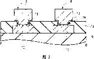
图2是沿着图1中的线A-A’所取的截面图;Fig. 2 is a sectional view taken along line A-A' among Fig. 1;
图3是沿着图1中的线B-B’所取的截面图;Fig. 3 is a sectional view taken along line B-B' among Fig. 1;
图4是图1中的线C所指示的区域的放大平面图,其示出导线形成于线性布置的凸点电极的正下方;FIG. 4 is an enlarged plan view of an area indicated by line C in FIG. 1, which shows that wires are formed right below linearly arranged bump electrodes;
图5是图1中的线D所指示的区域的放大平面图,其示出导线形成于以Z字形图案布置的凸点电极的正下方;FIG. 5 is an enlarged plan view of an area indicated by line D in FIG. 1, showing that wires are formed right below bump electrodes arranged in a zigzag pattern;
图6是表示在根据第一实施例的半导体器件制造工艺中的一个步骤的截面图;6 is a sectional view showing a step in the manufacturing process of the semiconductor device according to the first embodiment;
图7是表示在半导体器件制造工艺中图6中的步骤之后的步骤的截面图;7 is a cross-sectional view showing a step subsequent to the step in FIG. 6 in the semiconductor device manufacturing process;
图8是表示在半导体器件制造工艺中图7中的步骤之后的步骤的截面图;8 is a cross-sectional view showing a step subsequent to the step in FIG. 7 in the semiconductor device manufacturing process;
图9是表示在半导体器件制造工艺中图8中的步骤之后的步骤的截面图;9 is a cross-sectional view showing a step subsequent to the step in FIG. 8 in the semiconductor device manufacturing process;
图10是表示在半导体器件制造工艺中图9中的步骤之后的步骤的截面图;10 is a cross-sectional view showing a step subsequent to the step in FIG. 9 in the semiconductor device manufacturing process;
图11是表示在半导体器件制造工艺中图10中的步骤之后的步骤的截面图;11 is a cross-sectional view showing a step subsequent to the step in FIG. 10 in the semiconductor device manufacturing process;
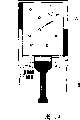
图12表示将半导体芯片安装在玻璃衬底上;Figure 12 shows that semiconductor chips are mounted on a glass substrate;
图13是安装在玻璃衬底上的半导体芯片的放大图;13 is an enlarged view of a semiconductor chip mounted on a glass substrate;
图14表示LCD的一般结构;Figure 14 shows the general structure of LCD;
图15表示另一类型LCD的一般结构;Figure 15 shows the general structure of another type of LCD;
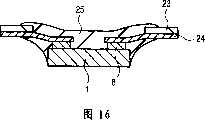
图16表示如何将半导体芯片安装到TCP(带式载体封装)形式的封装衬底上;Fig. 16 shows how to mount a semiconductor chip on a package substrate in the form of a TCP (Tape Carrier Package);
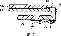
图17表示以TCP形式封装的半导体芯片位于玻璃衬底与印刷电路板之间的例子;17 shows an example in which a semiconductor chip packaged in a TCP form is located between a glass substrate and a printed circuit board;
图18表示如何将半导体芯片安装在COF(薄膜上芯片)形式的封装衬底上;Fig. 18 shows how to mount a semiconductor chip on a package substrate in the form of COF (chip on film);
图19表示以COF形式封装的半导体芯片位于玻璃衬底与印刷电路板之间的例子;Fig. 19 shows an example in which a semiconductor chip packaged in a COF form is located between a glass substrate and a printed circuit board;
图20是根据本发明的第二实施例的半导体芯片的局部平面图;20 is a partial plan view of a semiconductor chip according to a second embodiment of the present invention;
图21是表示第二实施例的一种变体的平面图;以及Fig. 21 is a plan view showing a modification of the second embodiment; and
图22是表示第二实施例的另一种变体的平面图。Fig. 22 is a plan view showing another modification of the second embodiment.
具体实施方式Detailed ways
以下将根据需要分别描述下述的优选实施例,但是除非另有说明,否则这些优选实施例并非是彼此不相关的。这些实施例在整体上或部分地是彼此的变体,并且有时一种描述是另一种描述的具体形式或补充形式。The following preferred embodiments will be described respectively as needed, but unless otherwise stated, these preferred embodiments are not independent of each other. These embodiments are variants of each other in whole or in part, and sometimes one description is a specific form or a supplementary form of another description.
同样,在下述的优选实施例中,即使在元件的数值数据(件数、数值、数量、范围等)是用特定的数值数字来表示时,除非另有说明或者其在理论上限于该特定的数值数字,否则这些数值数据都不限于所表示的特定数值数字;其可以大于或小于该特定的数值数字。Also, in the following preferred embodiments, even when the numerical data (number of pieces, numerical value, quantity, range, etc.) of elements is expressed with a specific numerical value, unless otherwise stated or it is theoretically limited to the specific numerical value Numerals, otherwise such numerical data are not limited to the particular numerical digits represented; they may be greater or less than the particular numerical digits.
在下述的优选实施例中,无需赘言,除非另有说明或在理论上必要,否则其组成元件(包括组成步骤)并非是必需的。In the following preferred embodiments, it goes without saying that unless otherwise stated or theoretically necessary, its constituent elements (including constituent steps) are not essential.
同样地,在下述的优选实施例中,当对某些元件指示特定的形式或位置关系时,除非另有说明或者除非从理论的观点看只应当使用该特定的形式或位置关系,否则其都应当解释为包括与这些特定形式或位置关系等同或相似的形式或位置关系。对于上面提到的数值或范围,情况也是如此。Likewise, in the following preferred embodiments, when specific forms or positional relationships are indicated for certain elements, unless otherwise specified or unless only the specific form or positional relationship should be used from a theoretical point of view, they are all It should be construed as including forms or positional relationships that are equivalent to or similar to these specific forms or positional relationships. The same is true for the values or ranges mentioned above.
接下来,将参考附图详细地描述本发明的优选实施例。在用于说明优选实施例的所有图中,基本上用相同的参考标号表示具有相同功能的元件,并且省略其重复描述。Next, preferred embodiments of the present invention will be described in detail with reference to the accompanying drawings. In all the drawings for explaining the preferred embodiments, elements having the same functions are basically denoted by the same reference numerals, and repeated descriptions thereof are omitted.
第一实施例first embodiment
图1是表示根据第一实施例的半导体芯片1(半导体器件)的结构的平面图。根据第一实施例的半导体芯片1是用于LCD的驱动器。参考图1,半导体芯片1具有半导体衬底2,该衬底例如采取拉长的矩形的形状,并且例如,在其主表面上形成驱动液晶显示器的LCD驱动器。该驱动器具有通过给构成LCD的单元阵列中的每个像素提供电压而控制液晶分子的定向的功能,并且该驱动器包括栅极驱动电路3、源极驱动电路4、液晶电路5、图形RAM(随机访问存储器)6以及外围电路7。FIG. 1 is a plan view showing the structure of a semiconductor chip 1 (semiconductor device) according to a first embodiment. The
在半导体芯片1的外围附近,沿着半导体芯片1的外围以规则的间隔布置多个凸点电极8。这些凸点电极8位于半导体芯片1的元件和互连导线所处的有源区域上方。多个凸点电极8包括用于集成电路的凸点电极,其对于集成电路配置来说是必需的,还包括假电极(dummyelectrode),其对于集成电路配置来说不是必需的。凸点电极8在半导体芯片1的一个长边和两个短边的附近以Z字形图案布置。以Z字形图案布置的多个凸点电极8主要作为用于栅极输出信号或源极输出信号的凸点电极来使用。围绕半导体芯片1的长边的中心以Z字形图案布置的凸点电极8是用于源极输出信号的凸点电极,而沿着半导体芯片1的长边、在其角的附近以Z字形图案布置的那些凸点电极8以及沿着半导体芯片1的短边以Z字形图案布置的那些凸点电极8是用于栅极输出信号的凸点电极。这种Z字形图案使得可以布置很多对栅极输出信号和源极输出信号来说必需的凸点电极,同时又不需要增大半导体芯片1的尺寸。换句话说,可以减小芯片尺寸并且同时增大凸点电极的数目。Near the periphery of the
在半导体芯片1的另一个长边的附近,不是以Z字形图案而是线性地布置凸点电极8。线性布置的凸点电极8是用于数字输入信号或模拟输入信号的凸点电极。同样,假凸点电极围绕半导体芯片1的四个角布置。在图1所示的例子中,用于栅极输出信号或源极输出信号的凸点电极8以Z字形图案布置,并且用于数字输入信号或模拟输入信号的凸点电极8线性地布置。然而,还可以是用于栅极输出信号或源极输出信号的凸点电极8线性地布置,而用于数字输入信号或模拟输入信号的凸点电极8以Z字形图案布置。In the vicinity of the other long side of the
图2是沿着图1中的线A-A’所取的截面图。在图2中,省略了顶层下方的层。尽管没有在图2中示出,但是在半导体衬底上方形成诸如MISFET(金属绝缘体半导体场效应晶体管)之类的半导体元件,并在该半导体元件上方制作多层互连。图2示出了在多层互连结构的顶层之上的多层互连。Fig. 2 is a sectional view taken along line A-A' in Fig. 1 . In Figure 2, the layers below the top layer are omitted. Although not shown in FIG. 2, a semiconductor element such as a MISFET (Metal Insulator Semiconductor Field Effect Transistor) is formed over a semiconductor substrate, and a multilayer interconnection is made over the semiconductor element. Figure 2 shows a multilayer interconnect over the top layer of the multilayer interconnect structure.
如图2所示,在例如氧化硅的绝缘膜9上方制作顶层互连布线。该顶层互连布线包括例如焊盘10和不同于焊盘10的导线11a和11b。导线11a和11b例如是用于信号的信号线或用于电源的电源线或假导线。焊盘10和导线11a、11b例如包括铝膜。As shown in FIG. 2, a top-level interconnection wiring is formed over an insulating
在焊盘10和导线11a、11b上方形成表面保护膜(钝化膜)12,使得覆盖焊盘10和导线11a、11b。例如,表面保护膜12包括氮化硅的绝缘膜。在表面保护膜12中制作开口13以露出焊盘10的表面,并通过UBM膜14作为内层(undercoat)金属膜,在包括开口13的内部的表面保护膜12上方形成凸点电极8。A surface protection film (passivation film) 12 is formed over the
在凸点电极8下方是包括焊盘10和导线11a、11b的布线层以及位于该包括焊盘10和导线11a、11b的布线层下方的多个其他的布线层(未示出)。类似地,在凸点电极8下方形成诸如上述的MISFET之类的半导体元件(未示出)。由此,本实施例使得可以通过有效地利用凸点电极8下方的空间而减小半导体芯片1的芯片面积。Below the
本发明的一个特点在于,开口13和焊盘10小于凸点电极8。传统地,在凸点电极8下方形成尺寸几乎等于凸点电极8的开口13,并且在开口13下方形成大于凸点电极8的焊盘10。换句话说,在凸点电极8下方形成焊盘10,并且焊盘10的尺寸与凸点电极8的尺寸几乎相同。然而,在构成LCD驱动器的半导体芯片1中,应当扩大凸点电极8以便确保其与玻璃衬底的粘着。因此,在凸点电极8下方的层中形成的焊盘10应当较大。如果焊盘10太大,则很难在多层互连的顶层中给不同于焊盘10的导线留下空间,并且因此,必须要增大半导体芯片1的尺寸。另一方面,在这个第一实施例中,如图2所示,开口13和焊盘10小于凸点电极8。换言之,凸点电极8大于焊盘10。以这种方式,当焊盘10小于凸点电极8时,在凸点电极8下方的层中为不同于焊盘10的导线11a、11b留下了空间。这可以如下文来进行。在传统的结构中,由于焊盘10位于凸点电极8正下方的顶层中,所以不可能在同一顶层中制作其他的导线。另一方面,在第一实施例中,由于焊盘10小于凸点电极8,所以在焊盘10所处的同一顶层中凸点电极8的正下方留出可用于其他导线11a、11b的形成的空间。因此,除了焊盘10以外,可以在凸点电极8正下方形成导线11a和11b,使得可以有效地利用凸点电极8正下方的空间,并可以减小半导体芯片1的尺寸。A feature of the present invention is that the
第一实施例的特征在于,凸点电极8的尺寸保持不变,并且焊盘10小于凸点电极8,为不同于用于凸点电极8的焊盘10的导线的形成留出空间。总之,在凸点电极8粘着到玻璃衬底的面积足够大的同时,为不同于焊盘10的导线留出空间以便可以减小半导体芯片1的尺寸。在前面的“背景技术”中引用的专利文献中既没有描述也没有暗示该技术思想,这是第一实施例所独有的。例如,可以通过增大凸点电极的尺寸而不改变焊盘尺寸,制作大于焊盘的凸点电极;然而,在这种情况下,焊盘本身的尺寸没有减小,并且不能获得由于减小焊盘尺寸而留出的空间。因此,不能减小半导体芯片的尺寸。此外,较大的凸点电极导致较大的半导体芯片,这意味着不可能减小半导体芯片的尺寸。如上所述,有两种方法可以实现小于凸点电极的焊盘电极:一种是增大凸点电极的尺寸,另一种是减小焊盘的尺寸。这两种方法在焊盘电极小于凸点电极方面是相同的,但是减小焊盘尺寸的那种方法与另一种方法的明显不同在于,在焊盘所处的同一层中在凸点电极下方为不同于焊盘的导线留出空间。此外,由于焊盘本身的尺寸减小,因此焊盘宽度可以小于不同于焊盘的相对宽的导线,诸如电源线。The first embodiment is characterized in that the size of the
图3是沿着图1的线B-B’所取的截面图。如图3所示,在沿着线B-B’所取的截面中,在绝缘膜9上方形成焊盘10,并且形成表面保护膜12使得覆盖焊盘10。在表面保护膜12中制作开口13,并在开口13的底部露出焊盘10的表面。在包括开口13的内部的表面保护膜12上方通过UBM膜14形成凸点电极8。在沿着线B-B’所取的截面的方向上,焊盘10的宽度几乎等于或大于凸点电极8的宽度。换句话说,在沿着图2中线A-A’所取的截面的方向上,焊盘10的宽度小于凸点电极8的宽度,并且在凸点电极8的正下方形成焊盘10以及其他信号线和电源线。另一方面,在沿着图3中的线B-B’所取的截面的方向上,在凸点电极8的正下方形成的焊盘10的宽度几乎等于凸点电极8的宽度。Fig. 3 is a sectional view taken along line B-B' of Fig. 1 . As shown in FIG. 3 , in a cross section taken along line B-B', a
图4是图1中的区域C的放大平面图,表示导线形成在线性布置的凸点电极8的正下方。如图4所示,矩形凸点电极8沿着短边方向(垂直于长边方向)并排排列。在凸点电极8下方形成表面保护膜12,并且在表面保护膜12中制作开口13。在形成于表面保护膜12中的开口13下方的层中形成焊盘10。焊盘10与部分地埋于开口中的凸点电极8电连接。焊盘10是方形的,并且其一个边稍微长于凸点电极8的短边。因此如图4所示,焊盘10的长度稍微大于凸点电极8的短边方向上的凸点电极8的长度。另一方面,焊盘10的长度远远小于凸点电极8的长边方向上的凸点电极8的长度。具体地,焊盘10小于凸点电极8,并且焊盘10只位于凸点电极8的一端的下方。因此,在凸点电极8的长边方向上,在焊盘10所处的同一布线层中留出空间。在该空间中形成不同于焊盘10的导线11a-11c。根据第一实施例,如上所述,可以在焊盘10所处的同一层中在凸点电极8的正下方形成导线11a-11c。由于可以有效地使用矩形大凸点电极8正下方的空间,因此可以减小半导体芯片的尺寸。FIG. 4 is an enlarged plan view of a region C in FIG. 1, showing that wires are formed right below the linearly arranged
导线11a-11c是信号线、电源线或假导线,并且可以具有不同的宽度。图4表示导线11c宽于导线11a和11b。传统地,焊盘尺寸与凸点电极8的尺寸相似,并且焊盘宽度与其他导线相比相对较大。另一方面,在本第一实施例中,焊盘10小于凸点电极8,并且在凸点电极8的正下方留出可用于形成导线的空间。因此,焊盘10的宽度可能小于例如在上述空间中形成的电源线的宽度。因此,根据第一实施例,焊盘10的宽度可以小于其它导线的宽度。The
导线11a-11c沿着与凸点电极8的长边方向垂直的方向延伸。尽管从有效利用空间的角度出发希望导线11a-11c能够垂直于凸点电极8的长边方向,但是它们并不一定要垂直于凸点电极8的长边方向。例如,依赖于互连图案,导线可以与凸点电极8的长边倾斜地交叉。即使在这种情况下,凸点电极8正下方的空间也是可用的,并且半导体芯片可以更小。Lead
图5是图1中的区域D的放大平面图,表示导线位于以Z字形图案布置的凸点电极8的正下方。如图5所示,如图4中那样,在凸点电极8的长边方向上,凸点电极8的宽度远远大于焊盘10的宽度,并且在焊盘10所处的同一层中在凸点电极8的长边方向上留出空间。在该空间中形成导线11d-11k。当凸点电极8以Z字形图案布置时,它们形成如图5所示的两行。因此,在凸点电极8的正下方留出的空间大于当凸点电极8形成一行时的情况。这意味着如果形成与凸点电极8的尺寸类似的焊盘,则将不可能在凸点电极8的正下方形成除了焊盘之外的其他导线。在这种情况下,当凸点电极8以Z字形图案布置时(这意味着它们布置成两行),可用于形成导线的空间将小于当凸点电极8布置成一行时的情况。然而,如图5所示,在第一实施例中,在第一行中的凸点电极8的正下方形成导线11d-11g,并且在第二行的凸点电极8的正下方形成导线11h-11k。因此,即使当凸点电极8以Z字形图案布置时,也可以几乎与当凸点电极8布置成一行时一样有效地使用凸点电极8正下方的空间。关于半导体芯片的凸点电极8,不仅可以在布置成一行的凸点电极8的下方,而且可以在布置成Z字形图案的凸点电极8的下方形成导线,并且由此可以减小半导体芯片的尺寸。FIG. 5 is an enlarged plan view of a region D in FIG. 1 , showing that the wires are located directly below the
图1中的区域D(图5)中的凸点电极8的数目大于图1的区域C(图4)中的凸点电极8的数目。这是因为在图1的区域D中需要更多的凸点电极8,以便驱动如图15所示的LCD屏幕区域20(稍后将描述)的元件。图1的区域D中的凸点电极8主要用于LCD屏幕区域20的元件的栅极和源极。The number of
接下来,将参考附图描述根据第一实施例的半导体器件的制造方法。例如,在单晶硅的半导体衬底上方形成诸如MISFET之类的半导体元件,并且在该半导体元件上方制作多层互连,尽管没有示出。图6表示在顶层中形成的导线,其中省略了顶层中的导线下方的层。Next, a method of manufacturing the semiconductor device according to the first embodiment will be described with reference to the drawings. For example, a semiconductor element such as a MISFET is formed over a semiconductor substrate of single-crystal silicon, and multilayer interconnections are made over the semiconductor element, although not shown. FIG. 6 shows the wires formed in the top layer, with layers below the wires in the top layer omitted.
例如,如图6所示,形成二氧化硅的绝缘膜9。可以使用CVD(化学汽相淀积)工艺形成绝缘膜9。可以在绝缘膜9上方叠置钛或氮化钛膜、铝膜和钛或氮化铁膜。然后,通过光刻或蚀刻在该叠置膜上进行构图,并且通过该构图工艺形成焊盘10和导线11a、11b。由此形成的焊盘10小于通过稍后将描述的工艺形成的凸点电极。导线11a和11b形成于凸点电极的正下方。For example, as shown in FIG. 6, an insulating
接下来,如图7所示,在其中形成焊盘10和导线11a、11b的绝缘膜9上方形成表面保护膜12。表面保护膜12例如包括氮化硅膜,并通过CVD工艺制成。接下来,通过光刻或蚀刻在表面保护膜12中制作一个开口13。该开口13位于焊盘10上方,并且使焊盘10的表面露出。开口13应当小于焊盘10。Next, as shown in FIG. 7 , a
接下来,如图8所示,在包括开口13的内部的表面保护膜12上方形成UBM(凸点下金属:under bump metal)膜14。UBM膜14通过溅射制成,并且包括钛、镍、钯、钛钨合金、氮化钛或金的单膜,或这些材料的叠层膜。UBM膜14不仅具有改善凸点电极8与焊盘10和表面保护膜12的粘着的功能,而且还具有可以抑制或防止由后续工艺制成的导电膜16的金属元件向导线11a、11b等的移动,或导线11a、11b等的金属元件向导电膜16的移动的阻挡功能。UBM膜14的平面图尺寸大于开口13的尺寸,并且几乎等于导电膜16的尺寸。Next, as shown in FIG. 8 , a UBM (under bump metal)
接着,如图9所示,在UBM膜14上方涂覆光刻胶(resist)膜15之后,通过对光刻胶膜15进行曝光和显影进行构图。以一种不会在凸点电极形成区域中留下光刻胶膜15的方式来进行构图。然后,如图10所示,例如,通过镀覆(plate)形成金膜作为导电膜16。然后,如图11所示,通过去除构图光刻胶膜15以及被光刻胶膜15覆盖的UBM膜14部分,可以形成包括导电膜16和UBM膜14的凸点电极8。接下来,通过对半导体衬底进行划片来生产单独的半导体芯片。Next, as shown in FIG. 9 , after coating a resist film 15 over the
根据第一实施例,由于在凸点电极8的正下方形成的焊盘10较小,因此可以在凸点电极8的下方形成导线11a和11b。可以在凸点电极8的正下方的同一层中形成焊盘10和导线11a、11b,以便能够有效地使用凸点电极8正下方留出的空间,并减小半导体芯片的尺寸。According to the first embodiment, since the
根据第一实施例的半导体器件制造方法与传统的半导体器件制造方法相同,除了以一种在凸点电极8的正下方形成焊盘10以及应当与焊盘10位于同一层中的导线11a和11b的方式来进行构图。因此,制造根据第一实施例的半导体器件不需要复杂的制造工艺。这意味着在不需要任何对制造工艺的重大改变的情况下可以获得有利的效果。The semiconductor device manufacturing method according to the first embodiment is the same as the conventional semiconductor device manufacturing method, except that the
接下来,将如上所述地生产的半导体芯片键合到封装衬底上。图12表示在玻璃衬底17a上方安装半导体芯片1(COG:玻璃上芯片)的情况。如图12所示,在玻璃衬底17a上安装玻璃衬底17b,形成一个LCD屏幕区域。将作为LCD驱动器的半导体芯片1安装到该LCD屏幕区域的附近的玻璃衬底17a上。半导体芯片1具有凸点电极8,其中凸点电极8通过各向异性导电膜19与玻璃衬底17a上形成的端子相连接。该玻璃衬底17a和柔性印刷电路板18同样通过各向异性导电膜19而连接。在以这种方式安装到玻璃衬底17a上的半导体芯片1中,用于输出的凸点电极8与LCD屏幕区域电连接,并且用于输入的凸点电极8与柔性印刷电路板18相连接。Next, the semiconductor chip produced as described above is bonded to the package substrate. FIG. 12 shows a state where a semiconductor chip 1 (COG: Chip On Glass) is mounted over a
图13是安装到玻璃衬底17a上的半导体芯片1的放大图。如图13所示,端子20a位于玻璃衬底17a上方,并且半导体芯片1的凸点电极8与端子20a电连接。在此,凸点电极8和端子20a不是直接连接,而是通过各向异性导电膜19而连接。FIG. 13 is an enlarged view of the
图14表示LCD的一般结构。如图14所示,LCD屏幕区域20位于玻璃衬底上方,并且图像显示在屏幕区域20上。将作为LCD驱动器的半导体芯片1安装在屏幕区域20的附近的玻璃衬底上方。将柔性印刷电路板18安装在半导体芯片1的附近,并且半导体芯片1作为驱动器位于印刷电路板18与LCD屏幕区域20之间。半导体芯片1可以以这种方式安装到玻璃衬底17a上方。Fig. 14 shows the general structure of an LCD. As shown in FIG. 14 , an
迄今为止,已经将LCD驱动器安装到封装衬底上的工艺作为COG的一个例子进行了说明,其中将半导体芯片1安装到玻璃衬底17a上。接下来,将说明封装半导体芯片1的其他形式的工艺。Hitherto, the process of mounting an LCD driver on a package substrate has been described as an example of COG in which the
图15示出了作为半导体芯片封装的非COG例子的TCP(带式载体封装)形式21和COF(薄膜上芯片)形式22。图16示出了如何将半导体芯片1安装到TCP形式的封装衬底上。参考图16,封装衬底是带状(带衬底)的薄膜衬底23,并且,例如,在薄膜衬底23上方形成铜的引线24。将半导体芯片1安装到薄膜衬底23上方,使得凸点电极8粘附到引线24。用树脂25密封半导体芯片1。图17示出了以TCP形式封装的半导体芯片1位于玻璃衬底17a与印刷电路板28之间的例子。如图17所示,玻璃衬底17a通过各向异性导电膜26与形成于薄膜衬底23上方的引线24连接,并且类似地,形成于薄膜衬底23上方的引线24通过各向异性导电膜27与印刷电路板28相连接。FIG. 15 shows a TCP (Tape Carrier Package)
图18示出了如何以COF形式将半导体芯片1安装到封装衬底上。参考图18,封装衬底是带状的薄膜衬底29。如在TCP形式中那样,铜的引线30位于薄膜衬底29上方,但是与TCP形式不同,将引线30固定在薄膜衬底29上正好与凸点电极8相连接的区域。以一种使凸点电极8粘附到引线30的方式将半导体芯片1安装到薄膜衬底29上方。在半导体芯片1与薄膜衬底29之间的间隙中有底层填料(underfill)31。图19示出了以COF形式将半导体芯片1安装到玻璃衬底17a与印刷电路板28之间的例子。如图19所示,玻璃衬底17a通过各向异性导电膜26与形成于薄膜衬底29上方的引线30相连接,并且类似地,形成于薄膜衬底29上方的引线30通过各向异性导电膜27与印刷电路板28相连接。FIG. 18 shows how to mount a
可以以如上所述的各种形式来封装作为LCD驱动器的半导体芯片1。The
第二实施例second embodiment
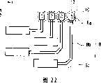
第二实施例涉及具有宽布局裕度的半导体器件,其与凸点电极位置无关地优化焊盘的位置。The second embodiment relates to a semiconductor device with a wide layout margin, which optimizes the position of the pad regardless of the position of the bump electrode.
图20是根据第二实施例的半导体芯片的局部平面图。参考图20,焊盘10通过形成在表面保护膜12中的开口13与作为凸点电极8的一部分的焊盘连接部分8a连接。凸点电极8包括:将与焊盘10连接的焊盘连接部分8a;将与封装衬底的端子连接的端子连接部分8c;以及连接焊盘连接部分8a与端子连接部分8c的布线部分8b。传统的凸点电极只包括连接焊盘的端子连接部分。换句话说,在传统的凸点电极中,端子连接部分还用作焊盘连接部分,这意味着焊盘连接部分与端子连接部分在平面上彼此重叠。另一方面,在根据第二实施例的凸点电极8中,焊盘连接部分8a与端子连接部分8c形成于如平面图中所见的不同位置,并且如平面图中所见的不同位置中的焊盘连接部分8a与端子连接部分8c通过布线部分8b连接。焊盘连接部分8a和端子连接部分8c在导线宽度上大于布线部分8b,如平面图中所见的那样。这是因为焊盘连接部分8a和端子连接部分8c必须分别与玻璃衬底(或薄膜衬底)上的焊盘10和引线连接,并且因此它们的平面表面必须足够大以确保连接。由于布线部分8b的导线宽度相对较小,因此不太可能与其他的布线部分8b接触,从而允许互连布线配置的较大裕度。Fig. 20 is a partial plan view of a semiconductor chip according to the second embodiment. Referring to FIG. 20 , the
由于这样来构造每个凸点电极8,因此焊盘10不以Z字形图案来布置,而是在X方向上布置成一行,同时凸点电极8的端子连接部分8c以Z字形图案布置。这意味着可以与凸点电极的位置无关地确定焊盘的位置。传统地,凸点电极和焊盘在平面上相互重叠;并且当凸点电极在Y方向上以Z字形图案布置时,焊盘也应当在Y方向上以Z字形图案布置。在这种情况下,焊盘布置成两行,并且不同于焊盘的导线不能位于焊盘所处的区域中。因此,在这种情况下,即使当焊盘形成得小于凸点电极以便如上所述地根据第一实施例形成不同于焊盘的导线,也不可能增大用于形成不同于焊盘的导线的空间,因为焊盘在Y方向上形成为两行。另一方面,根据第二实施例,即使当凸点电极8以Z字形图案布置时,焊盘10也不必以Z字形图案布置,而可以如图20所示的那样在X方向上布置成一行。因此,焊盘10所占的空间比焊盘10布置成两行的时候要小。由于焊盘10所占的空间较小,因此可以在焊盘10所处的同一层中在凸点电极8下方留出足够的空间来形成不同于焊盘10的导线11a-11k。因此,可以进一步减小半导体芯片的尺寸。形成于凸点电极8正下方的导线11a-11k不一定是线性的;它们可以是折叠或弯曲的。Since each
如上所述,本发明的一个特点在于,凸点电极8包括焊盘连接部分8a、布线部分8b以及端子连接部分8c,并且焊盘连接部分8a与端子连接部分8c在平面上不重叠。焊盘连接部分8a、布线部分8b以及端子连接部分8c在同一层中。这使得可以在Y方向上延伸的凸点电极8以Z字形图案布置,同时焊盘10在X方向上布置成一行。由于作为凸点电极8的一部分的端子连接部分8c键合到诸如玻璃衬底的封装衬底,因此其宽度形成得大于布线部分8b的宽度以及焊盘连接部分8a的宽度,以便确保所需的粘着力。可以如下来解释本实施例的凸点电极8包括焊盘连接部分8a、布线部分8b和端子连接部分8c的这一特点:凸点电极8包括较窄的布线部分(第一部分)8b以及宽于布线部分8b的端子连接部分(第二部分)8c。这使得与封装衬底接触的面积可以足够大,并且凸点电极8以较小的间隔以Z字形图案布置。换句话说,凸点电极8的端子连接部分8c相对较宽,因为端子连接部分8c将要键合到封装衬底,而布线部分8b的宽度相对较小,因为布线部分8b只是用于连接焊盘连接部分与端子连接部分,因此凸点电极8可以以较小的间隔以Z字形图案布置。As described above, a feature of the present invention is that
根据第二实施例,可以与凸点电极位置无关地确定焊盘的位置,使得有效地减小半导体芯片的尺寸。换句话说,由于允许焊盘配置的较大裕度,因此可以有效地减小半导体芯片的尺寸。此外,由于可以与焊盘10无关地增大凸点电极8的端子连接部分8c的面积,因此可以灵活地改变与封装衬底的接触面积。According to the second embodiment, the position of the pad can be determined independently of the position of the bump electrode, so that the size of the semiconductor chip can be effectively reduced. In other words, since a large margin in pad arrangement is allowed, the size of the semiconductor chip can be effectively reduced. Furthermore, since the area of the
根据第二实施例的半导体器件的制造方法几乎与在第一实施例中的相同。不同之处在于,凸点电极8包括焊盘连接部分8a、布线部分8b以及端子连接部分8c,并且焊盘连接部分8a与端子连接部分8c在平面上不重叠。此外,端子连接部分8c的宽度应当大于布线部分8b的宽度。制造根据第二实施例的半导体器件时考虑了这些方面。The manufacturing method of the semiconductor device according to the second embodiment is almost the same as that in the first embodiment. The difference is that the
接下来,将说明第二实施例的一个变体。图21是第二实施例的一个变体的平面图。图21示出了焊盘10在X方向上布置成一行并且凸点电极8的端子连接部分8c在Y方向上布置成一行的情况。该变体也是通过使用包括焊盘连接部分8a、布线部分8b和端子连接部分8c的凸点电极8来实现的。例如,即使当凸点电极8的端子连接部分8c在Y方向上布置成一行以便符合用户要求时,焊盘10也可以在X方向上布置成一行。焊盘10的位置可以与形成端子连接部分8c的位置无关地进行确定。同样,尽管在图21中没有示出,但不同于焊盘10的导线形成于焊盘10所处的同一层中的凸点电极8的正下方。因此,可以有效地利用凸点电极8正下方的空间,使得减小半导体芯片的尺寸。此外,由于这允许焊盘10的布局布置的较大裕度,因此可以通过优化焊盘10的位置来进一步减小半导体芯片的尺寸。图21表示出凸点电极8的布线部分8b弯曲成直角;然而,作为替代,它们也可以是成曲线的。Next, a modification of the second embodiment will be explained. Fig. 21 is a plan view of a modification of the second embodiment. FIG. 21 shows a case where
图22是表示第二实施例的另一个变体的平面图。图22示出了焊盘10在X方向上布置成一行并且凸点电极8的端子连接部分8c在Y方向上以Z字形图案布置的情况。该变体也是通过使用包括焊盘连接部分8a、布线部分8b以及端子连接部分8c的凸点电极8而实现的。例如,即使当凸点电极8的端子连接部分8c在Y方向上以Z字形图案布置以便符合用户要求时,焊盘10也可以在X方向上布置成一行。焊盘10的位置可以与形成端子连接部分8c的位置无关地进行确定。同样,尽管在图22中没有示出,但不同于焊盘10的导线形成于焊盘10所处的同一层中的凸点电极8的正下方。因此,可以有效地利用凸点电极8正下方的空间,使得减小半导体芯片的尺寸。此外,由于这允许焊盘10的布局布置的较大裕度,因此可以通过优化焊盘10的位置来进一步减小半导体芯片的尺寸。Fig. 22 is a plan view showing another modification of the second embodiment. FIG. 22 shows a case where
迄今为止,已经参照本发明的实施例对本发明人做出的本发明进行了详细的说明。然而,本发明不限于此,并且很明显,在不偏离本发明的精神和范围的情况下,可以以各种方式对这些细节进行修改。So far, the invention made by the present inventors has been described in detail with reference to the embodiments of the invention. However, the present invention is not limited thereto, and it is obvious that the details can be modified in various ways without departing from the spirit and scope of the present invention.
尽管在上述实施例中凸点电极8和焊盘10都沿着半导体芯片的四个边而定位,但是很明显本发明不限于这种情况。例如,焊盘10还可以位于半导体芯片1的四个边的附近,而凸点电极8延伸到半导体芯片1的中心。可选地,焊盘10还可以位于半导体芯片1的中心,而凸点电极8延伸到半导体芯片1的四个边。Although both the
在对上述实施例的描述中,假设了半导体器件用作LCD驱动器,但是本发明并不限于这种情况,并且本发明可以适用于具有凸点电极的各种各样的半导体器件。In the description of the above embodiments, it has been assumed that the semiconductor device is used as an LCD driver, but the present invention is not limited to this case, and the present invention can be applied to various semiconductor devices having bump electrodes.
本发明可以广泛地用于半导体制造工业。The present invention can be widely used in the semiconductor manufacturing industry.
Claims (22)
Applications Claiming Priority (2)
| Application Number | Priority Date | Filing Date | Title |
|---|---|---|---|
| JP2005294902AJP4708148B2 (en) | 2005-10-07 | 2005-10-07 | Semiconductor device |
| JP294902/2005 | 2005-10-07 |
Related Child Applications (2)
| Application Number | Title | Priority Date | Filing Date |
|---|---|---|---|
| CNA2008101685975ADivisionCN101388351A (en) | 2005-10-07 | 2006-09-29 | Semiconductor device and manufacturing method thereof |
| CN2009101597451ADivisionCN101593742B (en) | 2005-10-07 | 2006-09-29 | Semiconductor device and a method of manufacturing the same |
Publications (2)
| Publication Number | Publication Date |
|---|---|
| CN1945817Atrue CN1945817A (en) | 2007-04-11 |
| CN100536119C CN100536119C (en) | 2009-09-02 |
Family
ID=37944332
Family Applications (3)
| Application Number | Title | Priority Date | Filing Date |
|---|---|---|---|
| CN2009101597451AActiveCN101593742B (en) | 2005-10-07 | 2006-09-29 | Semiconductor device and a method of manufacturing the same |
| CNB2006101418119AActiveCN100536119C (en) | 2005-10-07 | 2006-09-29 | Semiconductor device and method for manufacturing the same |
| CNA2008101685975APendingCN101388351A (en) | 2005-10-07 | 2006-09-29 | Semiconductor device and manufacturing method thereof |
Family Applications Before (1)
| Application Number | Title | Priority Date | Filing Date |
|---|---|---|---|
| CN2009101597451AActiveCN101593742B (en) | 2005-10-07 | 2006-09-29 | Semiconductor device and a method of manufacturing the same |
Family Applications After (1)
| Application Number | Title | Priority Date | Filing Date |
|---|---|---|---|
| CNA2008101685975APendingCN101388351A (en) | 2005-10-07 | 2006-09-29 | Semiconductor device and manufacturing method thereof |
Country Status (5)
| Country | Link |
|---|---|
| US (12) | US20070080416A1 (en) |
| JP (1) | JP4708148B2 (en) |
| KR (2) | KR100933201B1 (en) |
| CN (3) | CN101593742B (en) |
| TW (4) | TWI578388B (en) |
Cited By (13)
| Publication number | Priority date | Publication date | Assignee | Title |
|---|---|---|---|---|
| CN101431058B (en)* | 2007-11-09 | 2012-12-26 | 瑞萨电子株式会社 | Semiconductor device and a method of manufacturing the same |
| CN103107721A (en)* | 2011-11-11 | 2013-05-15 | 株式会社电装 | Electric power converter having plurality of semiconductor modules arrayed in successive layers |
| CN103390599A (en)* | 2012-05-07 | 2013-11-13 | 联咏科技股份有限公司 | Chip on film device |
| CN103887251A (en)* | 2014-04-02 | 2014-06-25 | 华进半导体封装先导技术研发中心有限公司 | Fan-out-type wafer-level packaging structure and manufacturing process |
| CN103972212A (en)* | 2013-01-25 | 2014-08-06 | 台湾积体电路制造股份有限公司 | Methods and apparatus for transmission lines in packages |
| CN104241230A (en)* | 2013-06-07 | 2014-12-24 | 瑞萨Sp驱动器公司 | Semiconductor device, display device module and manufacture method thereof |
| CN105575884A (en)* | 2014-10-13 | 2016-05-11 | 中芯国际集成电路制造(上海)有限公司 | Hybrid interconnection structure, manufacturing method thereof, and electronic device comprising hybrid interconnection structure |
| CN105575944A (en)* | 2014-10-13 | 2016-05-11 | 中芯国际集成电路制造(上海)有限公司 | Hybrid interconnection structure, manufacturing method thereof, and electronic device comprising hybrid interconnection structure |
| CN105575883A (en)* | 2014-10-13 | 2016-05-11 | 中芯国际集成电路制造(上海)有限公司 | Hybrid interconnection structure, manufacturing method thereof, and electronic device comprising hybrid interconnection structure |
| CN106449575A (en)* | 2015-08-07 | 2017-02-22 | 晶宏半导体股份有限公司 | Bump structure of semiconductor device |
| CN108732833A (en)* | 2018-05-24 | 2018-11-02 | 京东方科技集团股份有限公司 | Array substrate and preparation method thereof, display device |
| CN110634826A (en)* | 2015-01-13 | 2019-12-31 | 野田士克林股份有限公司 | Semiconductor device with a plurality of transistors |
| CN113725186A (en)* | 2021-11-02 | 2021-11-30 | 北京智芯微电子科技有限公司 | Chip bonding pad structure, chip, wafer and chip bonding pad structure manufacturing method |
Families Citing this family (45)
| Publication number | Priority date | Publication date | Assignee | Title |
|---|---|---|---|---|
| JP4708148B2 (en) | 2005-10-07 | 2011-06-22 | ルネサスエレクトロニクス株式会社 | Semiconductor device |
| TWI378540B (en)* | 2006-10-14 | 2012-12-01 | Advanpack Solutions Pte Ltd | Chip and manufacturing method thereof |
| TW200847114A (en)* | 2007-05-30 | 2008-12-01 | Au Optronics Corp | A circuit signal connection interface, a manufacture method thereof, and an electronic device using the same |
| KR100798896B1 (en)* | 2007-06-07 | 2008-01-29 | 주식회사 실리콘웍스 | Pad Arrangement Structure of Semiconductor Chip |
| US8089156B2 (en)* | 2007-10-24 | 2012-01-03 | Panasonic Corporation | Electrode structure for semiconductor chip with crack suppressing dummy metal patterns |
| JP4585564B2 (en)* | 2007-12-13 | 2010-11-24 | ルネサスエレクトロニクス株式会社 | Semiconductor device |
| JP5395407B2 (en)* | 2008-11-12 | 2014-01-22 | ルネサスエレクトロニクス株式会社 | Semiconductor integrated circuit device for driving display device and manufacturing method of semiconductor integrated circuit device for driving display device |
| JP5331610B2 (en)* | 2008-12-03 | 2013-10-30 | ルネサスエレクトロニクス株式会社 | Semiconductor integrated circuit device |
| US8139370B2 (en)* | 2009-03-24 | 2012-03-20 | Viasat, Inc. | Electronic system having field effect transistors and interconnect bumps on a semiconductor substrate |
| JP5147779B2 (en)* | 2009-04-16 | 2013-02-20 | 新光電気工業株式会社 | Wiring board manufacturing method and semiconductor package manufacturing method |
| US20120080789A1 (en)* | 2009-06-16 | 2012-04-05 | Sharp Kabushiki Kaisha | SEMICONDUCTOR CHIP AND MOUNTING STRUCTURE OF THE SAME (as amended) |
| JP5503208B2 (en) | 2009-07-24 | 2014-05-28 | ルネサスエレクトロニクス株式会社 | Semiconductor device |
| JP5315186B2 (en) | 2009-09-18 | 2013-10-16 | ルネサスエレクトロニクス株式会社 | Manufacturing method of semiconductor device |
| JP5448788B2 (en)* | 2009-12-22 | 2014-03-19 | ルネサスエレクトロニクス株式会社 | Semiconductor device |
| US8193639B2 (en)* | 2010-03-30 | 2012-06-05 | Taiwan Semiconductor Manufacturing Company, Ltd. | Dummy metal design for packaging structures |
| DE102010013519B4 (en)* | 2010-03-31 | 2012-12-27 | Siltronic Ag | Method for polishing a semiconductor wafer |
| JP5746494B2 (en) | 2010-11-24 | 2015-07-08 | ルネサスエレクトロニクス株式会社 | Semiconductor device, liquid crystal display panel, and portable information terminal |
| US8647974B2 (en)* | 2011-03-25 | 2014-02-11 | Ati Technologies Ulc | Method of fabricating a semiconductor chip with supportive terminal pad |
| US20130193570A1 (en)* | 2012-02-01 | 2013-08-01 | Chipbond Technology Corporation | Bumping process and structure thereof |
| US20130292819A1 (en)* | 2012-05-07 | 2013-11-07 | Novatek Microelectronics Corp. | Chip-on-film device |
| KR20140041975A (en) | 2012-09-25 | 2014-04-07 | 삼성전자주식회사 | Bump structures and electrical connection structures having the bump structures |
| JP5466280B2 (en)* | 2012-10-29 | 2014-04-09 | ルネサスエレクトロニクス株式会社 | Semiconductor device |
| JP6180801B2 (en)* | 2013-06-07 | 2017-08-16 | ルネサスエレクトロニクス株式会社 | Semiconductor device |
| JP6305759B2 (en)* | 2013-12-26 | 2018-04-04 | 株式会社ジャパンディスプレイ | Display device |
| US20150187714A1 (en)* | 2013-12-26 | 2015-07-02 | Globalfoundries Singapore Pte. Ltd. | Integrated circuits including copper pillar structures and methods for fabricating the same |
| US9275967B2 (en) | 2014-01-06 | 2016-03-01 | Taiwan Semiconductor Manufacturing Company, Ltd. | Protrusion bump pads for bond-on-trace processing |
| US9418928B2 (en) | 2014-01-06 | 2016-08-16 | Taiwan Semiconductor Manufacturing Company, Ltd. | Protrusion bump pads for bond-on-trace processing |
| JP5759029B2 (en)* | 2014-01-23 | 2015-08-05 | ルネサスエレクトロニクス株式会社 | Semiconductor device |
| JP2015198122A (en)* | 2014-03-31 | 2015-11-09 | シナプティクス・ディスプレイ・デバイス合同会社 | semiconductor device |
| US9312251B2 (en)* | 2014-06-19 | 2016-04-12 | Shenzhen China Star Optoelectronics Technology Co., Ltd. | Display panel and manufacturing method thereof |
| JP5918421B2 (en)* | 2015-06-04 | 2016-05-18 | ルネサスエレクトロニクス株式会社 | Semiconductor device |
| JP5918422B2 (en)* | 2015-06-04 | 2016-05-18 | ルネサスエレクトロニクス株式会社 | Semiconductor device |
| JP6019183B2 (en)* | 2015-06-25 | 2016-11-02 | ルネサスエレクトロニクス株式会社 | Semiconductor device |
| KR102751172B1 (en) | 2016-11-30 | 2025-01-07 | 삼성디스플레이 주식회사 | Display device |
| US10490493B2 (en) | 2016-12-30 | 2019-11-26 | Innolux Corporation | Package structure and manufacturing method thereof |
| US10256179B2 (en)* | 2017-02-06 | 2019-04-09 | Nanya Technology Corporation | Package structure and manufacturing method thereof |
| US20180254257A1 (en)* | 2017-03-06 | 2018-09-06 | Innolux Corporation | Package structure and method of manufacturing package structure |
| TWI649738B (en)* | 2017-11-17 | 2019-02-01 | 英屬開曼群島商錼創科技股份有限公司 | Display panel and its repair method |
| JP7240487B2 (en)* | 2018-09-28 | 2023-03-15 | 華為技術有限公司 | GATE DRIVE CIRCUIT, METHOD FOR CONTROLLING GATE DRIVE CIRCUIT, AND MOBILE TERMINAL |
| KR102734417B1 (en)* | 2019-01-31 | 2024-11-26 | 삼성디스플레이 주식회사 | Display device |
| CN110111687B (en)* | 2019-05-22 | 2021-12-24 | 深圳秋田微电子股份有限公司 | Display device and preparation method thereof |
| CN110707100B (en)* | 2019-10-16 | 2021-12-31 | 友达光电(昆山)有限公司 | Display panel |
| DE102020135087A1 (en) | 2020-03-27 | 2021-09-30 | Samsung Electronics Co., Ltd. | Semiconductor package |
| US11581278B2 (en) | 2020-10-19 | 2023-02-14 | Micron Technology, Inc. | Semiconductor device and method of forming the same |
| KR20230021204A (en) | 2021-08-04 | 2023-02-14 | 삼성전자주식회사 | Chip On Film Package |
Family Cites Families (32)
| Publication number | Priority date | Publication date | Assignee | Title |
|---|---|---|---|---|
| JPH0494656A (en)* | 1990-08-10 | 1992-03-26 | Sawamura Juichi | Production of pumpkin noodle |
| JP2988075B2 (en)* | 1991-10-19 | 1999-12-06 | 日本電気株式会社 | Semiconductor device |
| US5485038A (en)* | 1993-07-15 | 1996-01-16 | Hughes Aircraft Company | Microelectronic circuit substrate structure including photoimageable epoxy dielectric layers |
| JP3046526B2 (en)* | 1995-06-21 | 2000-05-29 | 株式会社村上開明堂 | Heater control device for vehicle rearview mirror |
| JPH0922912A (en)* | 1995-07-05 | 1997-01-21 | Casio Comput Co Ltd | Semiconductor device and manufacturing method thereof |
| US6022792A (en)* | 1996-03-13 | 2000-02-08 | Seiko Instruments, Inc. | Semiconductor dicing and assembling method |
| JP3699237B2 (en) | 1996-03-13 | 2005-09-28 | セイコーインスツル株式会社 | Semiconductor integrated circuit |
| KR100255591B1 (en)* | 1997-03-06 | 2000-05-01 | 구본준 | Wiring connection structure of thin film transistor array and manufacturing method thereof |
| JP3063831B2 (en) | 1997-08-11 | 2000-07-12 | 日本電気株式会社 | Display device and manufacturing method thereof |
| JP3855495B2 (en)* | 1998-10-16 | 2006-12-13 | セイコーエプソン株式会社 | Semiconductor device, semiconductor mounting substrate using the same, liquid crystal display device, and electronic device |
| US6037668A (en)* | 1998-11-13 | 2000-03-14 | Motorola, Inc. | Integrated circuit having a support structure |
| JP4021104B2 (en)* | 1999-08-05 | 2007-12-12 | セイコーインスツル株式会社 | Semiconductor device having bump electrodes |
| JP2001110833A (en)* | 1999-10-06 | 2001-04-20 | Matsushita Electronics Industry Corp | Semiconductor device |
| JP2001144228A (en)* | 1999-11-12 | 2001-05-25 | Sanyo Electric Co Ltd | Semiconductor device and ite manufacturing method |
| JP2001185552A (en)* | 1999-12-27 | 2001-07-06 | Hitachi Ltd | Semiconductor integrated circuit device and method of manufacturing the same |
| JP2002198374A (en)* | 2000-10-16 | 2002-07-12 | Sharp Corp | Semiconductor device and method of manufacturing the same |
| US6501525B2 (en) | 2000-12-08 | 2002-12-31 | Industrial Technology Research Institute | Method for interconnecting a flat panel display having a non-transparent substrate and devices formed |
| JP4008245B2 (en)* | 2002-01-25 | 2007-11-14 | シャープ株式会社 | Display device drive device |
| KR100455678B1 (en)* | 2002-02-06 | 2004-11-06 | 마이크로스케일 주식회사 | Structure and method for manufacturing solder bump of flip chip package |
| JP2005101527A (en) | 2003-08-21 | 2005-04-14 | Seiko Epson Corp | Electronic component mounting structure, electro-optical device, electronic apparatus, and electronic component mounting method |
| KR100585104B1 (en) | 2003-10-24 | 2006-05-30 | 삼성전자주식회사 | Manufacturing method of ultra thin flip chip package |
| JP3880600B2 (en)* | 2004-02-10 | 2007-02-14 | 松下電器産業株式会社 | Semiconductor device and manufacturing method thereof |
| US6900541B1 (en)* | 2004-02-10 | 2005-05-31 | United Microelectronics Corp. | Semiconductor chip capable of implementing wire bonding over active circuits |
| JP4228948B2 (en)* | 2004-03-16 | 2009-02-25 | 日本電気株式会社 | Display device |
| JP3873986B2 (en) | 2004-04-16 | 2007-01-31 | セイコーエプソン株式会社 | Electronic component, mounting structure, electro-optical device, and electronic apparatus |
| US7452803B2 (en)* | 2004-08-12 | 2008-11-18 | Megica Corporation | Method for fabricating chip structure |
| US7241636B2 (en)* | 2005-01-11 | 2007-07-10 | Freescale Semiconductor, Inc. | Method and apparatus for providing structural support for interconnect pad while allowing signal conductance |
| US8319343B2 (en)* | 2005-09-21 | 2012-11-27 | Agere Systems Llc | Routing under bond pad for the replacement of an interconnect layer |
| JP4708148B2 (en)* | 2005-10-07 | 2011-06-22 | ルネサスエレクトロニクス株式会社 | Semiconductor device |
| JP2007214243A (en) | 2006-02-08 | 2007-08-23 | Renesas Technology Corp | Manufacturing method for semiconductor device |
| JP5123510B2 (en)* | 2006-09-28 | 2013-01-23 | ルネサスエレクトロニクス株式会社 | Semiconductor device |
| US8072035B2 (en)* | 2007-06-11 | 2011-12-06 | Renesas Electronics Corporation | Semiconductor device and method of manufacturing the same |
- 2005
- 2005-10-07JPJP2005294902Apatent/JP4708148B2/ennot_activeExpired - Lifetime
- 2006
- 2006-09-29CNCN2009101597451Apatent/CN101593742B/enactiveActive
- 2006-09-29CNCNB2006101418119Apatent/CN100536119C/enactiveActive
- 2006-09-29CNCNA2008101685975Apatent/CN101388351A/enactivePending
- 2006-10-04KRKR1020060097621Apatent/KR100933201B1/enactiveActive
- 2006-10-05TWTW105109509Apatent/TWI578388B/enactive
- 2006-10-05TWTW095137258Apatent/TWI382461B/enactive
- 2006-10-05TWTW101142762Apatent/TWI475604B/enactive
- 2006-10-05TWTW104102471Apatent/TWI538028B/enactive
- 2006-10-06USUS11/543,859patent/US20070080416A1/ennot_activeAbandoned
- 2007
- 2007-12-09USUS11/953,068patent/US7728442B2/enactiveActive
- 2007-12-09USUS11/953,055patent/US7538430B2/enactiveActive
- 2008
- 2008-05-19KRKR1020080046229Apatent/KR100861153B1/enactiveActive
- 2010
- 2010-04-23USUS12/766,567patent/US8183142B2/enactiveActive
- 2012
- 2012-02-14USUS13/396,456patent/US8338968B2/enactiveActive
- 2012-11-20USUS13/682,672patent/US8624403B2/enactiveActive
- 2013
- 2013-12-17USUS14/109,827patent/US9159650B2/enactiveActive
- 2015
- 2015-08-26USUS14/836,342patent/US9576924B2/enactiveActive
- 2016
- 2016-12-01USUS15/366,794patent/US9929185B2/enactiveActive
- 2018
- 2018-02-19USUS15/898,975patent/US10304867B2/enactiveActive
- 2019
- 2019-04-16USUS16/385,129patent/US20190244978A1/ennot_activeAbandoned
- 2020
- 2020-04-07USUS16/842,315patent/US10957719B2/enactiveActive
Cited By (33)
| Publication number | Priority date | Publication date | Assignee | Title |
|---|---|---|---|---|
| US8785318B2 (en) | 2007-11-09 | 2014-07-22 | Renesas Electronics Corporation | Semiconductor device and a method of manufacturing the same |
| US8552552B2 (en) | 2007-11-09 | 2013-10-08 | Renesas Electronics Corporation | Semiconductor device and a method of manufacturing the same |
| US8552555B2 (en) | 2007-11-09 | 2013-10-08 | Renesas Electronics Corporation | Semiconductor device and a method of manufacturing the same |
| US11239191B2 (en) | 2007-11-09 | 2022-02-01 | Renesas Electronics Corporation | Semiconductor device and a method of manufacturing the same |
| US9484286B2 (en) | 2007-11-09 | 2016-11-01 | Renesas Electronics Corporation | Semiconductor device and a method of manufacturing the same |
| US10741517B2 (en) | 2007-11-09 | 2020-08-11 | Renesas Electronics Corporation | Semiconductor device and a method of manufacturing the same |
| CN101431058B (en)* | 2007-11-09 | 2012-12-26 | 瑞萨电子株式会社 | Semiconductor device and a method of manufacturing the same |
| US10204878B2 (en) | 2007-11-09 | 2019-02-12 | Renesas Electronics Corporation | Semiconductor device and a method of manufacturing the same |
| US9508630B2 (en) | 2007-11-09 | 2016-11-29 | Renesas Electronics Corporation | Semiconductor device and a method of manufacturing the same |
| US9484287B2 (en) | 2007-11-09 | 2016-11-01 | Renesas Electronics Corporation | Semiconductor device and a method of manufacturing the same |
| CN103107721A (en)* | 2011-11-11 | 2013-05-15 | 株式会社电装 | Electric power converter having plurality of semiconductor modules arrayed in successive layers |
| CN103107721B (en)* | 2011-11-11 | 2015-06-17 | 株式会社电装 | Electric power converter having plurality of semiconductor modules arrayed in successive layers |
| CN103390599A (en)* | 2012-05-07 | 2013-11-13 | 联咏科技股份有限公司 | Chip on film device |
| US10269746B2 (en) | 2013-01-25 | 2019-04-23 | Taiwan Semiconductor Manufacturing Company, Ltd. | Methods and apparatus for transmission lines in packages |
| US11978712B2 (en) | 2013-01-25 | 2024-05-07 | Taiwan Semiconductor Manufacturing Company, Ltd. | Method of forming semiconductor package transmission lines with micro-bump lines |
| US10840201B2 (en) | 2013-01-25 | 2020-11-17 | Taiwan Semiconductor Manufacturing Company, Ltd. | Methods and apparatus for transmission lines in packages |
| CN103972212A (en)* | 2013-01-25 | 2014-08-06 | 台湾积体电路制造股份有限公司 | Methods and apparatus for transmission lines in packages |
| CN104241230A (en)* | 2013-06-07 | 2014-12-24 | 瑞萨Sp驱动器公司 | Semiconductor device, display device module and manufacture method thereof |
| CN104241230B (en)* | 2013-06-07 | 2018-11-09 | 辛纳普蒂克斯日本合同会社 | Semiconductor devices, display device module and its manufacturing method |
| CN103887251B (en)* | 2014-04-02 | 2016-08-24 | 华进半导体封装先导技术研发中心有限公司 | Fan-out-type wafer level packaging structure and manufacturing process |
| CN103887251A (en)* | 2014-04-02 | 2014-06-25 | 华进半导体封装先导技术研发中心有限公司 | Fan-out-type wafer-level packaging structure and manufacturing process |
| CN105575884B (en)* | 2014-10-13 | 2018-11-16 | 中芯国际集成电路制造(上海)有限公司 | A kind of mixing interconnection structure and its manufacturing method, electronic device |
| CN105575883B (en)* | 2014-10-13 | 2018-11-16 | 中芯国际集成电路制造(上海)有限公司 | A kind of mixing interconnection structure and its manufacturing method, electronic device |
| CN105575884A (en)* | 2014-10-13 | 2016-05-11 | 中芯国际集成电路制造(上海)有限公司 | Hybrid interconnection structure, manufacturing method thereof, and electronic device comprising hybrid interconnection structure |
| CN105575944B (en)* | 2014-10-13 | 2018-08-21 | 中芯国际集成电路制造(上海)有限公司 | A kind of mixing interconnection structure and its manufacturing method, electronic device |
| CN105575944A (en)* | 2014-10-13 | 2016-05-11 | 中芯国际集成电路制造(上海)有限公司 | Hybrid interconnection structure, manufacturing method thereof, and electronic device comprising hybrid interconnection structure |
| CN105575883A (en)* | 2014-10-13 | 2016-05-11 | 中芯国际集成电路制造(上海)有限公司 | Hybrid interconnection structure, manufacturing method thereof, and electronic device comprising hybrid interconnection structure |
| CN110634826A (en)* | 2015-01-13 | 2019-12-31 | 野田士克林股份有限公司 | Semiconductor device with a plurality of transistors |
| CN106449575B (en)* | 2015-08-07 | 2020-07-24 | 晶宏半导体股份有限公司 | Bump structure of semiconductor device |
| CN106449575A (en)* | 2015-08-07 | 2017-02-22 | 晶宏半导体股份有限公司 | Bump structure of semiconductor device |
| CN108732833A (en)* | 2018-05-24 | 2018-11-02 | 京东方科技集团股份有限公司 | Array substrate and preparation method thereof, display device |
| US11735597B2 (en) | 2018-05-24 | 2023-08-22 | Ordos Yuansheng Optoelectronics Co., Ltd. | Array substrate, display panel, display device and method of manufacturing an array substrate |
| CN113725186A (en)* | 2021-11-02 | 2021-11-30 | 北京智芯微电子科技有限公司 | Chip bonding pad structure, chip, wafer and chip bonding pad structure manufacturing method |
Also Published As
Similar Documents
| Publication | Publication Date | Title |
|---|---|---|
| CN1945817A (en) | Semiconductor device and manufacturing method thereof | |
| JP4094656B2 (en) | Semiconductor device | |
| CN1638103A (en) | Tape circuit substrate with reduced size of base film | |
| CN1992247A (en) | Heat-radiating semiconductor chip, tape wiring substrate and tape package using the same | |
| JP4585564B2 (en) | Semiconductor device | |
| TWI361476B (en) | Semiconductor package and display apparatus | |
| JP5259674B2 (en) | Semiconductor device | |
| US20250096085A1 (en) | Chip on film package and display apparatus including the same |
Legal Events
| Date | Code | Title | Description |
|---|---|---|---|
| C06 | Publication | ||
| PB01 | Publication | ||
| C10 | Entry into substantive examination | ||
| SE01 | Entry into force of request for substantive examination | ||
| C14 | Grant of patent or utility model | ||
| GR01 | Patent grant | ||
| ASS | Succession or assignment of patent right | Owner name:RENESAS ELECTRONICS Free format text:FORMER OWNER: RENESAS TECHNOLOGY CORP. Effective date:20100919 | |
| C41 | Transfer of patent application or patent right or utility model | ||
| COR | Change of bibliographic data | Free format text:CORRECT: ADDRESS; FROM: TOKYO, JAPAN TO: KANAGAWA PREFECTURE, JAPAN | |
| TR01 | Transfer of patent right | Effective date of registration:20100919 Address after:Kanagawa Patentee after:Renesas Electronics Corporation Address before:Tokyo, Japan, Japan Patentee before:Renesas Technology Corp. | |
| CP02 | Change in the address of a patent holder | Address after:Tokyo, Japan, Japan Patentee after:Renesas Electronics Corporation Address before:Kanagawa Patentee before:Renesas Electronics Corporation | |
| CP02 | Change in the address of a patent holder |