CN1941353A - Circuit board, and semiconductor device - Google Patents
Circuit board, and semiconductor deviceDownload PDFInfo
- Publication number
- CN1941353A CN1941353ACNA2006101399832ACN200610139983ACN1941353ACN 1941353 ACN1941353 ACN 1941353ACN A2006101399832 ACNA2006101399832 ACN A2006101399832ACN 200610139983 ACN200610139983 ACN 200610139983ACN 1941353 ACN1941353 ACN 1941353A
- Authority
- CN
- China
- Prior art keywords
- semiconductor element
- conductor wiring
- wiring
- auxiliary
- region
- Prior art date
- Legal status (The legal status is an assumption and is not a legal conclusion. Google has not performed a legal analysis and makes no representation as to the accuracy of the status listed.)
- Pending
Links
Images


Classifications
- H—ELECTRICITY
- H01—ELECTRIC ELEMENTS
- H01L—SEMICONDUCTOR DEVICES NOT COVERED BY CLASS H10
- H01L23/00—Details of semiconductor or other solid state devices
- H01L23/48—Arrangements for conducting electric current to or from the solid state body in operation, e.g. leads, terminal arrangements ; Selection of materials therefor
- H01L23/488—Arrangements for conducting electric current to or from the solid state body in operation, e.g. leads, terminal arrangements ; Selection of materials therefor consisting of soldered or bonded constructions
- H01L23/498—Leads, i.e. metallisations or lead-frames on insulating substrates, e.g. chip carriers
- H01L23/4985—Flexible insulating substrates
- H—ELECTRICITY
- H01—ELECTRIC ELEMENTS
- H01L—SEMICONDUCTOR DEVICES NOT COVERED BY CLASS H10
- H01L23/00—Details of semiconductor or other solid state devices
- H01L23/48—Arrangements for conducting electric current to or from the solid state body in operation, e.g. leads, terminal arrangements ; Selection of materials therefor
- H01L23/488—Arrangements for conducting electric current to or from the solid state body in operation, e.g. leads, terminal arrangements ; Selection of materials therefor consisting of soldered or bonded constructions
- H01L23/498—Leads, i.e. metallisations or lead-frames on insulating substrates, e.g. chip carriers
- H01L23/49811—Additional leads joined to the metallisation on the insulating substrate, e.g. pins, bumps, wires, flat leads
- H—ELECTRICITY
- H05—ELECTRIC TECHNIQUES NOT OTHERWISE PROVIDED FOR
- H05K—PRINTED CIRCUITS; CASINGS OR CONSTRUCTIONAL DETAILS OF ELECTRIC APPARATUS; MANUFACTURE OF ASSEMBLAGES OF ELECTRICAL COMPONENTS
- H05K1/00—Printed circuits
- H05K1/02—Details
- H05K1/11—Printed elements for providing electric connections to or between printed circuits
- H05K1/111—Pads for surface mounting, e.g. lay-out
- H—ELECTRICITY
- H01—ELECTRIC ELEMENTS
- H01L—SEMICONDUCTOR DEVICES NOT COVERED BY CLASS H10
- H01L2224/00—Indexing scheme for arrangements for connecting or disconnecting semiconductor or solid-state bodies and methods related thereto as covered by H01L24/00
- H01L2224/01—Means for bonding being attached to, or being formed on, the surface to be connected, e.g. chip-to-package, die-attach, "first-level" interconnects; Manufacturing methods related thereto
- H01L2224/02—Bonding areas; Manufacturing methods related thereto
- H01L2224/04—Structure, shape, material or disposition of the bonding areas prior to the connecting process
- H01L2224/05—Structure, shape, material or disposition of the bonding areas prior to the connecting process of an individual bonding area
- H01L2224/0554—External layer
- H01L2224/05573—Single external layer
- H—ELECTRICITY
- H01—ELECTRIC ELEMENTS
- H01L—SEMICONDUCTOR DEVICES NOT COVERED BY CLASS H10
- H01L2224/00—Indexing scheme for arrangements for connecting or disconnecting semiconductor or solid-state bodies and methods related thereto as covered by H01L24/00
- H01L2224/01—Means for bonding being attached to, or being formed on, the surface to be connected, e.g. chip-to-package, die-attach, "first-level" interconnects; Manufacturing methods related thereto
- H01L2224/10—Bump connectors; Manufacturing methods related thereto
- H01L2224/15—Structure, shape, material or disposition of the bump connectors after the connecting process
- H01L2224/16—Structure, shape, material or disposition of the bump connectors after the connecting process of an individual bump connector
- H—ELECTRICITY
- H01—ELECTRIC ELEMENTS
- H01L—SEMICONDUCTOR DEVICES NOT COVERED BY CLASS H10
- H01L23/00—Details of semiconductor or other solid state devices
- H01L23/48—Arrangements for conducting electric current to or from the solid state body in operation, e.g. leads, terminal arrangements ; Selection of materials therefor
- H01L23/488—Arrangements for conducting electric current to or from the solid state body in operation, e.g. leads, terminal arrangements ; Selection of materials therefor consisting of soldered or bonded constructions
- H01L23/498—Leads, i.e. metallisations or lead-frames on insulating substrates, e.g. chip carriers
- H01L23/49838—Geometry or layout
- H—ELECTRICITY
- H01—ELECTRIC ELEMENTS
- H01L—SEMICONDUCTOR DEVICES NOT COVERED BY CLASS H10
- H01L2924/00—Indexing scheme for arrangements or methods for connecting or disconnecting semiconductor or solid-state bodies as covered by H01L24/00
- H01L2924/01—Chemical elements
- H01L2924/01078—Platinum [Pt]
- H—ELECTRICITY
- H05—ELECTRIC TECHNIQUES NOT OTHERWISE PROVIDED FOR
- H05K—PRINTED CIRCUITS; CASINGS OR CONSTRUCTIONAL DETAILS OF ELECTRIC APPARATUS; MANUFACTURE OF ASSEMBLAGES OF ELECTRICAL COMPONENTS
- H05K1/00—Printed circuits
- H05K1/18—Printed circuits structurally associated with non-printed electric components
- H05K1/189—Printed circuits structurally associated with non-printed electric components characterised by the use of a flexible or folded printed circuit
- H—ELECTRICITY
- H05—ELECTRIC TECHNIQUES NOT OTHERWISE PROVIDED FOR
- H05K—PRINTED CIRCUITS; CASINGS OR CONSTRUCTIONAL DETAILS OF ELECTRIC APPARATUS; MANUFACTURE OF ASSEMBLAGES OF ELECTRICAL COMPONENTS
- H05K2201/00—Indexing scheme relating to printed circuits covered by H05K1/00
- H05K2201/03—Conductive materials
- H05K2201/0332—Structure of the conductor
- H05K2201/0364—Conductor shape
- H05K2201/0367—Metallic bump or raised conductor not used as solder bump
- H—ELECTRICITY
- H05—ELECTRIC TECHNIQUES NOT OTHERWISE PROVIDED FOR
- H05K—PRINTED CIRCUITS; CASINGS OR CONSTRUCTIONAL DETAILS OF ELECTRIC APPARATUS; MANUFACTURE OF ASSEMBLAGES OF ELECTRICAL COMPONENTS
- H05K2201/00—Indexing scheme relating to printed circuits covered by H05K1/00
- H05K2201/09—Shape and layout
- H05K2201/09209—Shape and layout details of conductors
- H05K2201/09654—Shape and layout details of conductors covering at least two types of conductors provided for in H05K2201/09218 - H05K2201/095
- H05K2201/09781—Dummy conductors, i.e. not used for normal transport of current; Dummy electrodes of components
- H—ELECTRICITY
- H05—ELECTRIC TECHNIQUES NOT OTHERWISE PROVIDED FOR
- H05K—PRINTED CIRCUITS; CASINGS OR CONSTRUCTIONAL DETAILS OF ELECTRIC APPARATUS; MANUFACTURE OF ASSEMBLAGES OF ELECTRICAL COMPONENTS
- H05K2201/00—Indexing scheme relating to printed circuits covered by H05K1/00
- H05K2201/10—Details of components or other objects attached to or integrated in a printed circuit board
- H05K2201/10613—Details of electrical connections of non-printed components, e.g. special leads
- H05K2201/10621—Components characterised by their electrical contacts
- H05K2201/10674—Flip chip
- Y—GENERAL TAGGING OF NEW TECHNOLOGICAL DEVELOPMENTS; GENERAL TAGGING OF CROSS-SECTIONAL TECHNOLOGIES SPANNING OVER SEVERAL SECTIONS OF THE IPC; TECHNICAL SUBJECTS COVERED BY FORMER USPC CROSS-REFERENCE ART COLLECTIONS [XRACs] AND DIGESTS
- Y02—TECHNOLOGIES OR APPLICATIONS FOR MITIGATION OR ADAPTATION AGAINST CLIMATE CHANGE
- Y02P—CLIMATE CHANGE MITIGATION TECHNOLOGIES IN THE PRODUCTION OR PROCESSING OF GOODS
- Y02P70/00—Climate change mitigation technologies in the production process for final industrial or consumer products
- Y02P70/50—Manufacturing or production processes characterised by the final manufactured product
Landscapes
- Engineering & Computer Science (AREA)
- Microelectronics & Electronic Packaging (AREA)
- Physics & Mathematics (AREA)
- Condensed Matter Physics & Semiconductors (AREA)
- General Physics & Mathematics (AREA)
- Computer Hardware Design (AREA)
- Power Engineering (AREA)
- Wire Bonding (AREA)
- Structure Of Printed Boards (AREA)
- Structures For Mounting Electric Components On Printed Circuit Boards (AREA)
Abstract
Translated fromChineseDescription
Translated fromChinese技术领域technical field
本发明涉及如薄膜上芯片(COF)所使用的带式载体基板那样的布线基板、及接合该布线基板及半导体元件的半导体器件。The present invention relates to a wiring substrate such as a tape carrier substrate used in a chip-on-film (COF), and a semiconductor device in which the wiring substrate and a semiconductor element are bonded.
背景技术Background technique
作为使用了薄膜基材的封装模块的一种已知有COF(Chip ONFilm)。图5是表示特开2004-327936号公报中所述的COF的一例的一部分的断面图。COF具有在利用柔软的绝缘性薄膜基材1制作的带式载体基板上安装有半导体元件4并由密封树脂5保护的结构,主要用作平板显示器的驱动用驱动器。COF (Chip ON Film) is known as one type of package module using a film base material. Fig. 5 is a cross-sectional view showing part of an example of the COF described in JP-A-2004-327936. The COF has a structure in which a
带式载体基板的主要的要素包括绝缘性的薄膜基材1、形成在其面上的导体布线2及该导体布线2上的突起电极3。根据需要,在导体布线2的一部分和突起电极3上形成有金属镀膜6,在导体布线2的其他部分形成有绝缘树脂的阻焊剂7的层。一般使用聚酰亚胺作为薄膜基材1,使用铜作为导体布线2。并且,突起电极3的形成方法一般是在薄膜基材1上形成导体布线2之后通过金属镀敷形成。The main elements of the tape carrier substrate include an insulating film substrate 1 ,
导体布线2通过突起电极3与半导体元件4上的电极焊盘8连接。连接方法一般是采用在带式载体基板上的半导体安装部涂敷密封树脂之后,使半导体元件4的电极焊盘8和带式载体基板的突起电极相对置,施加超声波、热及压力。
图6是示意地表示使半导体元件4上的电极焊盘8和带式载体基板上的突起电极3互相对置的状态的例子的平面图。但是,考虑到便于看清,是从薄膜基材1侧看省略了薄膜基材1的图示的图。如图6所示,半导体元件4的安装区域的多个导体布线2,一般是以直线状互相平行。6 is a plan view schematically showing an example of a state where electrode pads 8 on the
如上所述,在带式载体基板上安装半导体元件时,对半导体元件4的电极焊盘8和带式载体基板的突起电极3施加超声波、热和压力。这时,半导体元件4的角部特别容易集中由超声波和压力所造成的应力,最外侧的导体布线2容易断线。图7是表示半导体元件4的角部的导体布线2断线的状态。如图7所示,导体布线2的断线部位9沿着突起电极3的半导体元件4的外侧的边最容易出现。As described above, when the semiconductor element is mounted on the tape carrier substrate, ultrasonic waves, heat and pressure are applied to the
作为应对该故障的对策,可以考虑使配置在最外侧的导体布线2比其他导体布线2粗的方法。但是,在此情况下,如上所述突起电极3是在形成导体布线2之后用金属镀敷形成,所以,最外侧的导体布线2的突起电极3形成得比其他导体布线2的突起电极3高。由这样产生的突起电极3的台阶产生接触不良,不适合安装半导体元件4。As a countermeasure against this failure, it is conceivable to make the
并且,随着今后的引线间距变窄而导体布线2的宽度减小,则更容易发生上述断线部位9,成为问题。In addition, as the width of the
发明内容Contents of the invention
本发明的目的是提供一种布线基板,能够抑制由接合布线基板的突起电极和半导体元件的电极焊盘时的应力集中产生的、最外侧的导体布线的断线。An object of the present invention is to provide a wiring board capable of suppressing disconnection of the outermost conductor wiring due to stress concentration when bonding protruding electrodes of the wiring board and electrode pads of a semiconductor element.
本发明的布线基板,作为基本结构具有:挠性绝缘基材;排列设置在上述挠性绝缘基材上的多条导体布线;在上述各导体布线的位于安装半导体元件的区域的端部设置的突起电极;通过使形成在上述半导体元件的电极端子和上述突起电极接合,将上述半导体元件安装在上述导体布线上。The wiring substrate of the present invention has, as a basic structure: a flexible insulating base material; a plurality of conductor wirings arranged in a row on the flexible insulating base material; A protruding electrode; the semiconductor element is mounted on the conductor wiring by bonding an electrode terminal formed on the semiconductor element to the protruding electrode.
为了解决上述问题,本发明的第1构成的布线基板,还具有:辅助导体布线,与最外侧的上述导体布线的外侧邻接,位于安装上述半导体元件的区域的最外侧角部;以及辅助突起电极,在上述辅助导体布线上与上述导体布线上的上述突起电极排列形成;在上述辅助导体布线的、从上述辅助突起电极向上述半导体元件安装区域的外侧方向,在上述辅助突起电极的附近形成了终端;在上述辅助导体布线的、从上述辅助突起电极向上述半导体元件安装区域的内侧方向,在上述辅助突起电极的附近弯曲,并与邻接的最外侧的导体布线的前端连接。In order to solve the above-mentioned problems, the wiring board according to the first configuration of the present invention further includes: an auxiliary conductor wiring adjacent to the outside of the outermost conductor wiring and located at the outermost corner of the region where the semiconductor element is mounted; and an auxiliary bump electrode. , formed on the above-mentioned auxiliary conductor wiring in alignment with the above-mentioned protruding electrodes on the above-mentioned conductor wiring; in the direction of the outside of the above-mentioned auxiliary conductor wiring from the above-mentioned auxiliary protruding electrodes to the above-mentioned semiconductor element mounting area, formed in the vicinity of the above-mentioned auxiliary protruding electrodes The terminal is bent in the vicinity of the auxiliary protruding electrode in the inner direction from the auxiliary protruding electrode toward the semiconductor element mounting region of the auxiliary conductor wiring, and is connected to the tip of the adjacent outermost conductor wiring.
本发明的第2结构的布线基板,位于安装上述半导体元件的区域的最外侧角部的最外侧的上述导体布线,从上述突起电极向上述半导体元件安装区域的外侧方向,在上述突起电极的附近形成了终端;从上述突起电极向上述半导体元件安装区域的内侧方向弯曲,与安装上述半导体元件的区域的排列了上述突起电极的边邻接的边相交叉并向外延伸。In the wiring board according to the second configuration of the present invention, the outermost conductor wiring located at the outermost corner of the region where the semiconductor element is mounted is located in the vicinity of the protrusion electrode from the protrusion electrode toward the outside of the semiconductor element mounting region. A terminal is formed; bent from the protruding electrodes toward the inside of the semiconductor device mounting region, intersects the side adjacent to the side where the protruding electrodes are arranged in the region where the semiconductor device is mounted, and extends outward.
本发明的第3构成的布线基板,位于安装上述半导体元件的区域的最外侧角部的最外侧的上述导体布线,从上述突起电极向上述半导体元件安装区域的外侧方向,在从上述突起电极到安装上述半导体元件的区域的边缘,具有至少一个弯曲部。In the wiring board according to the third configuration of the present invention, the outermost conductor wiring positioned at the outermost corner of the region where the semiconductor element is mounted is arranged from the protruding electrode toward the outer side of the semiconductor element mounting region, from the protruding electrode to the outermost direction of the semiconductor element mounting region. The edge of the region where the semiconductor element is mounted has at least one bent portion.
附图说明Description of drawings
图1是表示本发明实施方式1的带式载体基板的一部分的平面图。FIG. 1 is a plan view showing part of a tape carrier substrate according to Embodiment 1 of the present invention.
图2是表示将该带式载体基板的一部分变形的例子的平面图。Fig. 2 is a plan view showing an example in which part of the tape carrier substrate is deformed.
图3是表示本发明实施方式2的带式载体基板的一部分的平面图。3 is a plan view showing part of a tape carrier substrate according to
图4是表示本发明实施方式3的带式载体基板的一部分的平面图。4 is a plan view showing part of a tape carrier substrate according to
图5是表示使用了现有例的带式载体基板的半导体器件的一部分的断面图。5 is a cross-sectional view showing part of a semiconductor device using a conventional tape carrier substrate.
图6是表示使用了现有例的带式载体基板的一部分的平面图。Fig. 6 is a plan view showing part of a tape carrier substrate using a conventional example.
图7是表示现有例的半导体器件的一部分的平面图。FIG. 7 is a plan view showing part of a conventional semiconductor device.
具体实施方式Detailed ways
本发明的第1结构的布线基板具有:位于半导体元件安装区域的最外侧角部的辅助导体布线、及形成在上述辅助导体布线上的辅助突起电极。在上述辅助导体布线的、从辅助突起电极向外侧方向,在上述辅助突起电极的附近形成了终端;在上述辅助导体布线的、从上述辅助突起电极向上述半导体元件安装区域的内侧方向弯曲,并与邻接的最外侧的导体布线的前端相连接,所以,通过辅助突起电极的配置能够减小对最外侧的导体布线的应力集中,抑制断线。The wiring board according to the first configuration of the present invention includes auxiliary conductor wiring located at the outermost corner of the semiconductor element mounting region, and auxiliary bump electrodes formed on the auxiliary conductor wiring. In the direction of the auxiliary conductor wiring outward from the auxiliary protrusion electrode, a terminal is formed near the auxiliary protrusion electrode; the auxiliary conductor wiring is bent inward from the auxiliary protrusion electrode to the semiconductor element mounting region, and Since it is connected to the tip of the adjacent outermost conductor wiring, stress concentration on the outermost conductor wiring can be reduced and disconnection can be suppressed by disposing the auxiliary protruding electrodes.
希望在第1结构的布线基板中,在上述辅助导体布线的、从上述辅助突起电极向上述半导体元件安装区域的外侧方向,在超过上述辅助突起电极的、长度大于0μm小于300μm的范围的位置形成了终端。In the wiring board of the first structure, it is desirable that the auxiliary conductor wiring is formed at a position exceeding the range of the auxiliary protrusion electrode and having a length greater than 0 μm and less than 300 μm in the direction outside the auxiliary protrusion electrode toward the semiconductor element mounting region. terminal.
并且,希望在上述辅助导体布线的上述半导体元件安装区域的外侧方向的终端的延长线上,具有与上述辅助导体布线不连续形成的假导体布线部。Furthermore, it is desirable to have a dummy conductor wiring portion formed discontinuously from the auxiliary conductor wiring on an extension line of the terminal of the auxiliary conductor wiring in the outer direction of the semiconductor element mounting region.
若采用本发明的第2结构的布线基板,最外侧的上述导体布线在从上述突起电极向上述半导体元件安装区域的外侧方向,在上述突起电极的附近形成了终端,在从上述突起电极向上述半导体元件安装区域的内侧方向弯曲,并同安装半导体元件的区域的、与上述突起电极排列的边相邻接的边进行交叉,向外延伸。这样一来,能够避开向最外侧的导体布线的应力集中的部位的布线,采用另外的路线,能够避免由应力集中造成的断线。According to the wiring board according to the second configuration of the present invention, the outermost conductor wiring is terminated in the vicinity of the protruding electrode in the direction from the protruding electrode to the outside of the semiconductor element mounting region, The inner side of the semiconductor element mounting region is curved, intersects with the side adjacent to the side where the protruding electrodes are arranged in the semiconductor element mounting region, and extends outward. In this way, it is possible to avoid wiring to a stress-concentrated portion of the outermost conductor wiring and to use a different route, thereby avoiding disconnection due to stress concentration.
希望在本发明的第2构成的布线基板中,位于安装上述半导体元件的区域的最外侧角部的最外侧的上述导体布线,从上述突起电极向上述半导体元件安装区域的外侧方向,在超过上述突起电极的、长度大于0μm小于300μm的范围的位置形成了终端。In the wiring board according to the second configuration of the present invention, it is desirable that the conductor wiring located on the outermost side of the outermost corner of the region where the semiconductor element is mounted exceeds the above-mentioned The position of the protruding electrode in the range of length greater than 0 μm and less than 300 μm forms a terminal.
并且,希望在上述最外侧的导体布线的、从上述突起电极向上述半导体元件安装区域的外侧方向的终端的延长线上,具有与上述最外侧的导体布线不连续形成的假导体布线部。In addition, it is desirable to have a dummy conductor wiring portion formed discontinuously from the outermost conductor wiring on an extension line of the outermost conductor wiring from the protruding electrode toward an outer terminal of the semiconductor element mounting region.
若采用第3构成的布线基板,位于最外侧角部的最外侧的上述导体布线,从上述突起电极向上述半导体元件安装区域的外侧方向,在从上述突起电极到安装上述半导体元件的区域的边缘,具有至少一个弯曲部。通过在最外侧的导体布线的应力集中的部位上配置弯曲部,能够缓和应力集中,抑制断线。In the wiring board according to the third configuration, the outermost conductor wiring located at the outermost corner portion is located on the edge of the area from the protrusion electrode to the semiconductor element mounting area in the direction outward from the protrusion electrode to the semiconductor element mounting area. , having at least one bend. By arranging the bent portion at the stress-concentrated portion of the outermost conductor wiring, stress concentration can be alleviated and disconnection can be suppressed.
本发明的半导体器件具有:上述任一结构的布线基板、以及安装在上述布线基板上的半导体元件,上述半导体元件的电极焊盘和上述导体布线通过上述突起电极连接。A semiconductor device according to the present invention includes: a wiring board having any one of the structures described above; and a semiconductor element mounted on the wiring board, wherein electrode pads of the semiconductor element and the conductor lines are connected via the protruding electrodes.
以下参照附图,详细说明本发明的实施方式。但是,对于根据图5~图7说明的现有例的部件相同的部件,标注相同的符号省略详细说明。Embodiments of the present invention will be described in detail below with reference to the drawings. However, the same components as those in the conventional example described with reference to FIGS. 5 to 7 are denoted by the same reference numerals, and detailed description thereof will be omitted.
(实施方式1)(Embodiment 1)
参照图1,详细说明实施方式1的带式载体基板(布线基板)的结构。图1是表示实施方式1的带式载体基板的半导体元件安装部的平面图。但考虑到便于看清,从薄膜基材1(参见图5)侧看的结构,省略薄膜基材1的图示,仅示意地表示导体布线2和突起电极3与半导体元件4上的电极焊盘8的关系。在以下的实施方式中也一样进行图示。Referring to FIG. 1, the structure of the tape carrier board (wiring board) of Embodiment 1 will be described in detail. FIG. 1 is a plan view showing a semiconductor element mounting portion of a tape carrier substrate according to Embodiment 1. FIG. However, considering the ease of seeing, the structure seen from the side of the film substrate 1 (see FIG. 5 ) omits the illustration of the film substrate 1, and only schematically shows the
如图1所示,与半导体元件4上的电极焊盘8相对应,在多个导体布线2上形成有各突起电极3。在最外侧的导体布线10的外侧,即与半导体元件4的最外边角部相对应的位置配置有辅助导体布线11,形成有辅助突起电极12。在辅助导体布线11的、从辅助突起电极12朝向半导体元件4安装区域的外侧的一侧,在辅助突起电极12的附近形成了终端。从辅助突起电极12向半导体元件4安装区域的内侧方向的端部弯曲,与邻接的最外侧的导体布线10的前端相连接。但是,连接辅助导体布线11的导体布线不仅限于邻接的一条导体布线10,也可以包括位于半导体元件4的同一边上的其他导体布线2形成多条导体布线。辅助导体布线11和辅助突起电极12与通常的导体布线2和突起电极3一样形成。As shown in FIG. 1 , each
在以上结构的情况下,在连接半导体元件4的电极焊盘8和布线基板上的突起电极3时,最外侧的导体布线10的突起电极3的端部通过邻接的辅助突起电极12缓和连接时的应力。并且,在从辅助突起电极12向半导体元件4的内侧的区域,实验证明最外侧的导体布线10不易断线,能确保导体布线的导通。In the case of the above structure, when connecting the
而且,虽未图示,希望辅助导体布线11设计成从突起电极3的设计位置突出这样的量,即,形成辅助突起电极12的工序的形成位置偏移量。但是,通过实验已确认,从突起电极3的设计位置的突出量可以设为300μm以下,如此也具有充分的效果。Furthermore, although not shown, it is desirable to design the
图2是表示图1所示的方式的变形例。该例的结构是,从辅助导体布线11的辅助突起电极12,在半导体元件安装区域的外侧方向延长线上,附加了假导体布线部13。FIG. 2 shows a modified example of the form shown in FIG. 1 . In the structure of this example, a dummy conductor wiring portion 13 is added on an extension line in the outer direction of the semiconductor element mounting region from the auxiliary protruding
假导体布线13未与辅助导体布线11上的辅助突起电极12连接。但是,与邻接的最外侧的导体布线10形成为相同的图形。在图2所示的结构的情况下,半导体元件4的角部的导体布线实质上成为连续的图形,所以,在安装半导体器件4时,布线基板的热膨胀不论部位而均匀。其结果,能够避免接合时的突起电极3和电极焊盘8的局部位置偏移。而且,虽未图示,假导体布线13也可以在未图示的区域外与最外侧的导体布线10、或其他导体布线2相连接。The dummy conductor wiring 13 is not connected to the
(实施方式2)(Embodiment 2)
参照图3说明实施方式2的带式载体基板(布线基板)的结构。图3是表示实施方式2的带式载体基板的半导体元件安装部的平面图。The configuration of the tape carrier board (wiring board) according to
在本实施方式中,在与半导体元件4的最外侧角部对应的位置配置的最外侧的导体布线14,其结构不同于其他通常的导体布线2。也就是说,在最外侧的导体布线14中,从突起电极3向半导体器件4安装区域的外侧方向(图的上方),在突起电极3的附近形成了终端。在从突起电极3向半导体元件4安装区域的内侧方向,向同半导体元件4安装区域的与排列了突起电极3的边邻接的边(图的侧边)相交叉的方向弯曲,向外延伸形成了弯曲布线部14a。In the present embodiment, the outermost conductor wiring 14 arranged at a position corresponding to the outermost corner of the
在该结构的情况下,在最外侧的导体布线14,在比突起电极3靠内侧的半导体器件4的区域,导体布线很难断线,所以,能够确保最外侧的导体布线14的导通。而且,与最外侧的导体布线14相邻接的导体布线2,也由于最外侧的导体布线14上的突起电极3和电极焊盘8的抵接而缓和应力,所以能够确保导体布线2的导通。With this configuration, the outermost conductor wiring 14 is less likely to be disconnected in the region of the
而且,虽未图示,希望最外侧的导体布线14设计成从突起电极3的设计位置突出这样的量,即,形成突起电极3的工序的形成位置偏移量以上。通过实验已确认,从突起电极3的设计位置的突出量可以设计成300μm以下,如此也具有充分的效果。Furthermore, although not shown, it is desirable that the outermost conductor wiring 14 is designed to protrude from the designed position of the protruding
再者,虽未图示与图2一样,从最外侧的导体布线14的突起电极3在半导体器件安装区域的外侧方向延长线上,未与突起电极3相连接,但是,能够附加具有与邻接的导体布线2相同图形的假导体布线部。这样,半导体元件4的角部的导体布线成为实质上连续的图形,所以在安装半导体元件4时,布线基板的热膨胀不论部位而均匀。其结果,能够避免接合时的突起电极3和电极焊盘8的局部位置偏移。Furthermore, although not shown, as in FIG. 2, the protruding
(实施方式3)(Embodiment 3)
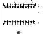
关于实施方式3的带式载体基板(布线基板)的结构,参照图4进行说明。图4是表示实施方式3的带式载体基板的半导体元件安装部的平面图。The configuration of the tape carrier board (wiring board) according to
在本实施方式中,在半导体元件4的与最外侧角部对应的位置配置的最外侧的导体布线15,其结构不同于其他通常的导体布线2。也就是说,最外侧的导体布线15从突起电极3到半导体元件4的安装区域的边缘,具有至少一个弯曲部15a。最外侧的导体布线15的半导体元件4的安装区域内侧的端部,不同于通常的导体布线2的结构。In the present embodiment, the
在这种结构的情况下,最外侧的导体布线15的突起电极3受到的应力由弯曲部15a缓和,所以能够确保最外侧的导体布线15的导通。而且,与最外侧的导体布线15相邻接的导体布线2也由于最外侧的导体布线15上的突起电极3和电极焊盘8的抵接缓和应力,因此,能够确保导体布线2的导通。In the case of such a structure, since the stress received by the protruding
通过以上实施方式,在向布线基板安装半导体元件时能够抑制最外部的导体布线的断线,能够提供具有可靠性的半导体器件。According to the above embodiments, disconnection of the outermost conductor wiring can be suppressed when mounting the semiconductor element on the wiring board, and a reliable semiconductor device can be provided.
Claims (10)
Translated fromChineseApplications Claiming Priority (2)
| Application Number | Priority Date | Filing Date | Title |
|---|---|---|---|
| JP287854/2005 | 2005-09-30 | ||
| JP2005287854AJP4740708B2 (en) | 2005-09-30 | 2005-09-30 | Wiring board and semiconductor device |
Publications (1)
| Publication Number | Publication Date |
|---|---|
| CN1941353Atrue CN1941353A (en) | 2007-04-04 |
Family
ID=37901126
Family Applications (1)
| Application Number | Title | Priority Date | Filing Date |
|---|---|---|---|
| CNA2006101399832APendingCN1941353A (en) | 2005-09-30 | 2006-09-28 | Circuit board, and semiconductor device |
Country Status (5)
| Country | Link |
|---|---|
| US (2) | US7439611B2 (en) |
| JP (1) | JP4740708B2 (en) |
| KR (1) | KR20070037310A (en) |
| CN (1) | CN1941353A (en) |
| TW (1) | TW200721427A (en) |
Families Citing this family (10)
| Publication number | Priority date | Publication date | Assignee | Title |
|---|---|---|---|---|
| JP5164523B2 (en)* | 2006-12-15 | 2013-03-21 | キヤノン株式会社 | Inkjet recording head |
| JP4994968B2 (en)* | 2007-06-21 | 2012-08-08 | キヤノン株式会社 | Inkjet printhead manufacturing method |
| KR101468875B1 (en)* | 2008-03-14 | 2014-12-10 | 삼성전자주식회사 | Flip Chip Package |
| JP4775408B2 (en)* | 2008-06-03 | 2011-09-21 | ソニー株式会社 | Display device, wiring layout method in display device, and electronic apparatus |
| KR102201116B1 (en) | 2019-01-23 | 2021-01-08 | 한국화학연구원 | A process for reducing hazardous substances such as odor vapors and particle matters from asphalt and the system thereof |
| KR102299697B1 (en) | 2019-05-09 | 2021-09-08 | 한국화학연구원 | A process for producing asphalt having less odor vapors and hazardous substances using additives possessing both polar and non-polar functional groups |
| KR102176906B1 (en) | 2019-04-16 | 2020-11-10 | 인성에이앤티 주식회사 | Apparatus for removing bad smell of ascon and method the same |
| KR102458793B1 (en) | 2019-11-18 | 2022-10-25 | 김영중 | Offensive odor and dust removal method generated during ascon manufacturing process |
| KR20240001549A (en)* | 2022-06-27 | 2024-01-03 | 엘지이노텍 주식회사 | Flexible printed circuit board, cof module and electronic device comprising the same |
| KR102493032B1 (en) | 2022-07-15 | 2023-01-31 | 주식회사 메트로엔지니어링 | Gravel circulation dry electrostatic precipitator |
Family Cites Families (15)
| Publication number | Priority date | Publication date | Assignee | Title |
|---|---|---|---|---|
| US5138438A (en)* | 1987-06-24 | 1992-08-11 | Akita Electronics Co. Ltd. | Lead connections means for stacked tab packaged IC chips |
| JPH02137345A (en)* | 1988-11-18 | 1990-05-25 | Nec Corp | Tab-type semiconductor device |
| JPH02205333A (en)* | 1989-02-03 | 1990-08-15 | Hitachi Cable Ltd | Tape carrier for TAB |
| JPH04364744A (en)* | 1991-06-12 | 1992-12-17 | Seiko Epson Corp | Structure of TAB implementation |
| JPH05136312A (en)* | 1991-11-15 | 1993-06-01 | Sony Corp | Semiconductor device |
| JPH0897252A (en)* | 1994-09-28 | 1996-04-12 | Fuji Xerox Co Ltd | Film carrier |
| JPH08316270A (en)* | 1995-05-23 | 1996-11-29 | Hitachi Ltd | Tape carrier and semiconductor device using the same |
| JPH0955407A (en)* | 1995-08-17 | 1997-02-25 | Mitsubishi Electric Corp | Tape carrier structure |
| JPH10199912A (en)* | 1997-01-16 | 1998-07-31 | Hitachi Ltd | Semiconductor device |
| JP3638750B2 (en)* | 1997-03-25 | 2005-04-13 | 株式会社ルネサステクノロジ | Semiconductor device |
| JP2002026083A (en)* | 2000-07-05 | 2002-01-25 | Seiko Epson Corp | Semiconductor device and its manufacturing method, circuit board, and electronic equipment |
| US6451626B1 (en)* | 2001-07-27 | 2002-09-17 | Charles W.C. Lin | Three-dimensional stacked semiconductor package |
| SG120879A1 (en)* | 2002-08-08 | 2006-04-26 | Micron Technology Inc | Packaged microelectronic components |
| JP3565835B1 (en) | 2003-04-28 | 2004-09-15 | 松下電器産業株式会社 | Wiring board, method of manufacturing the same, semiconductor device and method of manufacturing the same |
| JP4786976B2 (en)* | 2005-09-13 | 2011-10-05 | パナソニック株式会社 | WIRING BOARD, MANUFACTURING METHOD THEREOF, AND SEMICONDUCTOR DEVICE |
- 2005
- 2005-09-30JPJP2005287854Apatent/JP4740708B2/ennot_activeExpired - Fee Related
- 2006
- 2006-09-06KRKR1020060085470Apatent/KR20070037310A/ennot_activeWithdrawn
- 2006-09-08TWTW095133141Apatent/TW200721427A/enunknown
- 2006-09-22USUS11/534,288patent/US7439611B2/enactiveActive
- 2006-09-28CNCNA2006101399832Apatent/CN1941353A/enactivePending
- 2008
- 2008-09-09USUS12/283,043patent/US20090020318A1/ennot_activeAbandoned
Also Published As
| Publication number | Publication date |
|---|---|
| US20070075439A1 (en) | 2007-04-05 |
| JP2007103431A (en) | 2007-04-19 |
| TW200721427A (en) | 2007-06-01 |
| US20090020318A1 (en) | 2009-01-22 |
| US7439611B2 (en) | 2008-10-21 |
| JP4740708B2 (en) | 2011-08-03 |
| KR20070037310A (en) | 2007-04-04 |
Similar Documents
| Publication | Publication Date | Title |
|---|---|---|
| CN1941353A (en) | Circuit board, and semiconductor device | |
| CN1227956C (en) | Flexible wiring board, manufacturing method thereof, and display device with flexible wiring board | |
| CN1182579C (en) | Substrate, display device, mounting and bonding method of substrate and IC chip | |
| CN1873967A (en) | Wiring board, semiconductor device, and display module | |
| CN102099905B (en) | Semiconductor device and display device | |
| US20110204497A1 (en) | Semiconductor integrated circuit and method for manufacturing the same | |
| US20090011591A1 (en) | Film substrate, fabrication method thereof, and image display substrate | |
| CN1913138A (en) | Semiconductor device | |
| CN1591841A (en) | Tape circuit substrate and semiconductor chip package using the same | |
| US7176568B2 (en) | Semiconductor device and its manufacturing method, electronic module, and electronic unit | |
| CN114501772A (en) | Flexible printed circuit boards, COF modules and electronic devices including the same | |
| CN101499453B (en) | Printed circuit board and method of manufacturing the same | |
| CN101055862A (en) | Wiring board, semiconductor device using the same, and method for manufacturing wiring board | |
| CN1433073A (en) | Semiconductor device and its making process, circuit board and electronic instrument | |
| TWI378546B (en) | Substrate and package for micro bga | |
| US6853080B2 (en) | Electronic device and method of manufacturing the same, and electronic instrument | |
| US7119423B2 (en) | Semiconductor device and method of manufacturing the same, electronic module, and electronic instrument | |
| JP4488073B2 (en) | Electrical connection device | |
| CN1301047C (en) | Welding disk pattern structure and substrate for carrging electrical components | |
| CN100433950C (en) | Film substrate, fabrication method thereof, and image display substrate | |
| CN1551341A (en) | Semiconductor device, electronic device, electronic device, and method for manufacturing semiconductor device | |
| KR101587269B1 (en) | FLEXIBLE TAPE CARRIER PACKAGE, METHOD FOR MANUFACTURING THE SAME, AND FLEXIBLE TAPE CARRIER | |
| KR20240028215A (en) | Flexible printed circuit board, cof module and electronic device comprising the same | |
| CN1747155A (en) | Substrate with Pad Strengthening Structure | |
| KR20250063243A (en) | Flexible circuit board for chip integration and electronic device having the same |
Legal Events
| Date | Code | Title | Description |
|---|---|---|---|
| C06 | Publication | ||
| PB01 | Publication | ||
| C10 | Entry into substantive examination | ||
| SE01 | Entry into force of request for substantive examination | ||
| AD01 | Patent right deemed abandoned | Effective date of abandoning:20070404 | |
| C20 | Patent right or utility model deemed to be abandoned or is abandoned |