CN1941281B - Method for forming alignment key of semiconductor device - Google Patents
Method for forming alignment key of semiconductor deviceDownload PDFInfo
- Publication number
- CN1941281B CN1941281BCN2006101431876ACN200610143187ACN1941281BCN 1941281 BCN1941281 BCN 1941281BCN 2006101431876 ACN2006101431876 ACN 2006101431876ACN 200610143187 ACN200610143187 ACN 200610143187ACN 1941281 BCN1941281 BCN 1941281B
- Authority
- CN
- China
- Prior art keywords
- layer
- capacitor
- substrate
- forming
- alignment keys
- Prior art date
- Legal status (The legal status is an assumption and is not a legal conclusion. Google has not performed a legal analysis and makes no representation as to the accuracy of the status listed.)
- Active
Links
Images


Classifications
- H—ELECTRICITY
- H01—ELECTRIC ELEMENTS
- H01L—SEMICONDUCTOR DEVICES NOT COVERED BY CLASS H10
- H01L23/00—Details of semiconductor or other solid state devices
- H01L23/544—Marks applied to semiconductor devices or parts, e.g. registration marks, alignment structures, wafer maps
- G—PHYSICS
- G03—PHOTOGRAPHY; CINEMATOGRAPHY; ANALOGOUS TECHNIQUES USING WAVES OTHER THAN OPTICAL WAVES; ELECTROGRAPHY; HOLOGRAPHY
- G03F—PHOTOMECHANICAL PRODUCTION OF TEXTURED OR PATTERNED SURFACES, e.g. FOR PRINTING, FOR PROCESSING OF SEMICONDUCTOR DEVICES; MATERIALS THEREFOR; ORIGINALS THEREFOR; APPARATUS SPECIALLY ADAPTED THEREFOR
- G03F9/00—Registration or positioning of originals, masks, frames, photographic sheets or textured or patterned surfaces, e.g. automatically
- G03F9/70—Registration or positioning of originals, masks, frames, photographic sheets or textured or patterned surfaces, e.g. automatically for microlithography
- G03F9/7073—Alignment marks and their environment
- H—ELECTRICITY
- H10—SEMICONDUCTOR DEVICES; ELECTRIC SOLID-STATE DEVICES NOT OTHERWISE PROVIDED FOR
- H10D—INORGANIC ELECTRIC SEMICONDUCTOR DEVICES
- H10D84/00—Integrated devices formed in or on semiconductor substrates that comprise only semiconducting layers, e.g. on Si wafers or on GaAs-on-Si wafers
- H10D84/80—Integrated devices formed in or on semiconductor substrates that comprise only semiconducting layers, e.g. on Si wafers or on GaAs-on-Si wafers characterised by the integration of at least one component covered by groups H10D12/00 or H10D30/00, e.g. integration of IGFETs
- H10D84/811—Combinations of field-effect devices and one or more diodes, capacitors or resistors
- H—ELECTRICITY
- H01—ELECTRIC ELEMENTS
- H01L—SEMICONDUCTOR DEVICES NOT COVERED BY CLASS H10
- H01L2223/00—Details relating to semiconductor or other solid state devices covered by the group H01L23/00
- H01L2223/544—Marks applied to semiconductor devices or parts
- H01L2223/54453—Marks applied to semiconductor devices or parts for use prior to dicing
- H01L2223/5446—Located in scribe lines
- H—ELECTRICITY
- H01—ELECTRIC ELEMENTS
- H01L—SEMICONDUCTOR DEVICES NOT COVERED BY CLASS H10
- H01L2924/00—Indexing scheme for arrangements or methods for connecting or disconnecting semiconductor or solid-state bodies as covered by H01L24/00
- H01L2924/0001—Technical content checked by a classifier
- H01L2924/0002—Not covered by any one of groups H01L24/00, H01L24/00 and H01L2224/00
Landscapes
- Physics & Mathematics (AREA)
- General Physics & Mathematics (AREA)
- Condensed Matter Physics & Semiconductors (AREA)
- Engineering & Computer Science (AREA)
- Computer Hardware Design (AREA)
- Microelectronics & Electronic Packaging (AREA)
- Power Engineering (AREA)
- Semiconductor Integrated Circuits (AREA)
- Metal-Oxide And Bipolar Metal-Oxide Semiconductor Integrated Circuits (AREA)
- Exposure And Positioning Against Photoresist Photosensitive Materials (AREA)
- Exposure Of Semiconductors, Excluding Electron Or Ion Beam Exposure (AREA)
Abstract
Translated fromChinese
Description
Translated fromChinese技术领域technical field
本发明涉及无需额外的工艺过程形成具有覆盖层的对准键的方法,和制造包括具有覆盖层的对准键的半导体器件的方法。The present invention relates to a method of forming an alignment key with a capping layer without an additional process, and a method of manufacturing a semiconductor device including the alignment key with a capping layer.
背景技术Background technique
由于半导体器件变得密集和高度集成,所以设计规则可以按比例缩小,单元元件可以变得很小。因此,在制造时在半导体衬底和掩模之间需要精确的对准。通常,对准键形成在半导体衬底的划线道中,用于对准半导体衬底和掩模。对准键之一可以形成在与经浅沟槽隔离(STI)工艺等用于限制芯片区的有源区的隔离层一起的划线道中,并可以具有在衬底上方突出的形状。对准键可以用于栅形成工艺、离子注入工艺、用于选择硅化物形成工艺的硅化阻挡层(SBL)、接触形成工艺等。As semiconductor devices become dense and highly integrated, design rules can be scaled down and unit elements can be made very small. Therefore, precise alignment is required between the semiconductor substrate and the mask at the time of manufacture. Typically, alignment keys are formed in scribe lanes of the semiconductor substrate for aligning the semiconductor substrate and the mask. One of the alignment keys may be formed in a scribe lane together with an isolation layer for limiting an active area of a chip area through a shallow trench isolation (STI) process or the like, and may have a shape protruding above a substrate. The alignment key may be used in a gate forming process, an ion implantation process, a silicide barrier layer (SBL) for a selective silicide forming process, a contact forming process, and the like.
因为功率器件例如LCD驱动IC(LDI)等需要用于驱动逻辑电路的低电压操作和用于驱动LCD运行的高电压操作,因此必须使用双栅氧化层。形成双栅氧化层的常规方法可以包括在半导体衬底的芯片区中形成限定有源区的隔离层,和在划线道中同时形成突出对准键。在衬底上形成第一热氧化层之后,除在芯片区域的高电压区域中之外可以湿法蚀刻第一热氧化层,从而形成用于高电压操作的第一栅氧化层。第二热氧化层可以形成在衬底上,从而在低电压区域中形成用于低电压操作的栅氧化层。在高电压区域中第一栅氧化层可以由厚的第一热氧化层形成,在低电压区域中第二栅氧化层可以由薄的第二热氧化层形成。Because power devices such as LCD driver ICs (LDIs) require low-voltage operation for driving logic circuits and high-voltage operation for driving LCD operations, dual gate oxide layers must be used. A conventional method of forming a double gate oxide layer may include forming an isolation layer defining an active region in a chip region of a semiconductor substrate, and simultaneously forming a protruding alignment key in a scribe lane. After forming the first thermal oxide layer on the substrate, the first thermal oxide layer may be wet etched except in the high voltage area of the chip area, thereby forming a first gate oxide layer for high voltage operation. A second thermal oxide layer may be formed on the substrate to form a gate oxide layer for low voltage operation in the low voltage region. The first gate oxide layer may be formed of a thick first thermal oxide layer in the high voltage region, and the second gate oxide layer may be formed of a thin second thermal oxide layer in the low voltage region.
然而,因为形成双栅氧化层的常规方法可以包括为了除去对准键的氧化物层的一部分,使用湿法刻蚀工艺除去低电压区域的第一热氧化层,所以可能降低在衬底表面和对准键之间的台阶高度差。在形成对准键之后,当执行随后的湿法刻蚀工艺时,可能损耗对准键的氧化物层。如果氧化物层的磨损显著,则因为在重复湿法刻蚀工艺过程中可能除去对准键的台阶高度差,因此对准键可以变得与衬底表面相平。如果对准键的台阶高度差被除去,则在随后工艺过程中不能精确地对准,可能发生未对准。However, since the conventional method of forming the dual gate oxide may include removing the first thermal oxide layer in the low voltage region using a wet etch process in order to remove a portion of the oxide layer for the alignment bond, there may be a reduction in the substrate surface and Align the step height difference between the keys. After the alignment key is formed, when a subsequent wet etching process is performed, the oxide layer of the alignment key may be lost. If wear of the oxide layer is significant, the alignment keys may become level with the substrate surface because the step height differences of the alignment keys may be removed during repeated wet etch processes. If the step height difference of the alignment key is removed, accurate alignment cannot be performed in a subsequent process, and misalignment may occur.
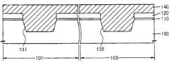
图1A-1F说明形成半导体器件的对准键的常规方法。参照图1A,在半导体衬底100上可以形成衬垫氧化物层110和硬掩模层120。可以使用光刻法等刻蚀硬掩模层120和衬垫氧化物层110,以暴露芯片区域101中的半导体衬底100的一部分,和划线道105中的半导体衬底100的一部分。可以刻蚀暴露的半导体衬底100,从而在芯片区域101中形成第一沟槽131,和在划线道105中形成第二沟槽135。1A-1F illustrate a conventional method of forming an alignment key of a semiconductor device. Referring to FIG. 1A , a
参照图1B,在硬掩模层120上可形成氧化物层140以填充第一沟槽131和第二沟槽135。参照图1C,使用化学机械抛光(CMP)等刻蚀氧化物层140以平面化衬底的表面。因而,可以在第一沟槽131内部形成第一隔离层141,可以在第二沟槽135内部形成第二隔离层145。第一隔离层141可以限定芯片区域101的有源区。Referring to FIG. 1B , an
参照图1D,可以除去硬掩模层120和衬垫氧化物层110。参照图1E,在衬底上沉积光敏层150,并将其图案化以暴露划线道105的第二隔离层145。参照图1F,可以使用光敏层150作为掩模刻蚀暴露的第二隔离层145,从而形成对准键135a。对准键135a可以具有凹槽结构,该凹槽结构相对于衬底表面具有H1的台阶高度差。可以完全地刻蚀第二隔离层145,对准键135a可以具有与第二沟槽135的深度对应的台阶高度差。Referring to FIG. 1D , the
因为将传统的对准键135a凹入以具有低于衬底表面的台阶高度差,当在随后的湿法刻蚀工艺过程中损耗隔离层145的氧化物层时可以仅仅增加台阶高度差。因此,可以避免对准键135a的台阶高度差降低的上述问题,但是因为需要额外的掩模形成工艺过程来形成凹陷的对准键135a,所以工艺过程复杂。Since the conventional alignment key 135a is recessed to have a step difference below the substrate surface, the step difference may only be increased when the oxide layer of the
发明内容Contents of the invention
本发明的示范性实施例提供了没有额外的掩模形成工艺过程而形成用于覆盖对准键的半导体器件的对准键的方法。示范性实施例还提供制造包括当形成用于在芯片区域中形成元件的图案时制造包含在划线道内形成对准键的覆盖层的半导体器件的方法。Exemplary embodiments of the present invention provide a method of forming an alignment key for a semiconductor device covering the alignment key without an additional mask forming process. Exemplary embodiments also provide a method of manufacturing a semiconductor device including manufacturing a capping layer including an alignment key formed in a scribe lane when forming a pattern for forming an element in a chip region.
根据示范性实施例,提供一种形成半导体器件的对准键的方法,其包括:在半导体衬底的芯片区域中形成限定有源区的隔离层,并且在划线道中形成相对于半导体衬底的表面具有台阶高度差的对准键。用于元件的至少一个形成层可以形成在衬底上,并可以转换,以在芯片区域中的半导体衬底上形成元件形成图案。覆盖对准键的覆盖层可以形成在划线道内的半导体衬底上。对准键相对于衬底可以具有大约50

至少一个形成层可以是至少一个绝缘层或者导电层。可以通过图案化和/或刻蚀转换用于元件的至少一个形成层。至少一个形成层可以是至少一个绝缘层并且至少一个绝缘层可以是氮化物层。至少一个形成层可以是导电层并且该导电层可以是多晶硅层。至少一个形成层和覆盖层可以由相对于对准键具有刻蚀选择率的材料组成。对准键可以包含氧化物层等,覆盖层可以包含至少一个形成层,或者可以包含包括至少一个形成层的堆叠层。至少一个形成层可以包括用于形成半导体器件的栅电极或者栅绝缘层的材料、或者用于形成半导体器件的电容器的底电极的材料,或者用于形成半导体器件的电容器的介质层的材料、或者包括用于形成电容器的底电极的材料和/或用于形成半导体器件的介质层的材料的堆叠结构。栅电极可以包括栅氧化层和/或栅绝缘层。The at least one forming layer may be at least one insulating layer or conductive layer. At least one formation layer for elements may be converted by patterning and/or etching. At least one formation layer may be at least one insulating layer and at least one insulating layer may be a nitride layer. At least one forming layer may be a conductive layer and the conductive layer may be a polysilicon layer. At least one of the formation layer and the capping layer may be composed of a material having etch selectivity with respect to the alignment keys. The alignment key may include an oxide layer or the like, and the cover layer may include at least one formation layer, or may include a stacked layer including at least one formation layer. At least one forming layer may comprise a material for forming a gate electrode or a gate insulating layer of a semiconductor device, or a material for forming a bottom electrode of a capacitor of a semiconductor device, or a material for forming a dielectric layer of a capacitor of a semiconductor device, or A stack structure comprising materials for forming a bottom electrode of a capacitor and/or materials for forming a dielectric layer of a semiconductor device. The gate electrode may include a gate oxide layer and/or a gate insulating layer.
形成隔离层和对准键可以包括在衬底上形成衬垫氧化物层和硬掩模层,以衬底上其中形成隔离层和对准键的部分。可以刻蚀衬底的暴露部分以在芯片区域中形成第一沟槽和在划线道内形成第二沟槽。隔离层可以在形成第一沟槽中,对准键可以形成在第二沟槽中。硬掩模层可以具有大约500

附图说明Description of drawings
通过参照附图详细描写示范性实施例将使示范性实施例的上述和其他的特征和优点变得更明显,其中:The above and other features and advantages of exemplary embodiments will become more apparent by describing in detail exemplary embodiments with reference to the accompanying drawings, in which:
图1A-1F说明形成传统的半导体器件的对准键的方法;1A-1F illustrate a method of forming an alignment key of a conventional semiconductor device;
图2A-2F说明根据示范性实施例形成半导体器件的对准键的方法;2A-2F illustrate a method of forming an alignment key of a semiconductor device according to an exemplary embodiment;
图3A-3F说明根据示范性实施例制造半导体器件的方法;3A-3F illustrate a method of fabricating a semiconductor device according to an exemplary embodiment;
图4A-4D说明根据示范性实施例制造半导体器件的方法;和4A-4D illustrate a method of fabricating a semiconductor device according to an exemplary embodiment; and
图5A-5F说明根据示范性实施例制造半导体器件的方法。5A-5F illustrate a method of fabricating a semiconductor device according to an exemplary embodiment.
具体实施方式Detailed ways
现在参照附图更全面地描述各个示范性实施例,其中显示了一些示范性实施例。然而,可以以许多不同的形式实现示范性实施例,且示范性实施例将不应解释为限于在这里阐述的实施例。相反,提供这些实施例以便全面和完全地公开,本公开将示范性实施例的范围完全地传达给本领域的技术人员。整个说明书中相同的数字表示相同的元件。Various exemplary embodiments will now be described more fully with reference to the accompanying drawings, in which some exemplary embodiments are shown. Example embodiments may, however, be embodied in many different forms and should not be construed as limited to the embodiments set forth herein. Rather, these embodiments are provided so that this disclosure will be thorough and complete, and this disclosure will fully convey the scope of the exemplary embodiments to those skilled in the art. Like numbers refer to like elements throughout the specification.
在这里可以使用空间地相对术语,例如“在...之下”、“在...下面”、“下层”、“在...之上”、“上面”等便于描述图中所述的一个元件或者部件与另一元件或者部件的关系。应该理解,空间相对术语除图中描述的方向之外还包含使用中或操作中的器件的不同的方向。例如,如果翻转图中的器件,则描述为“在其他的元件或者部件下面”或者“在其他的元件或者部件之下”将朝向“在其他的元件或者部件之上”。因而,实例术语“在...下面”可以包含高于和低于两个方向。器件可以另外定向(旋转90°或者在其他的方向),并因此解释这里所使用的空间相对描述符。Spatially relative terms may be used here, such as "under", "under", "lower", "on", "above", etc. to facilitate the description of what is described in the drawings The relationship of one element or part to another element or part. It will be understood that spatially relative terms encompass different orientations of the device in use or operation in addition to the orientation depicted in the figures. For example, if the device in the figures is turned over, descriptions of "beneath" or "beneath other elements or features" would then be oriented "above the other elements or features". Thus, the example term "below" can encompass both an orientation of above and below. Devices may be otherwise oriented (rotated 90° or at other orientations), and thus interpret the spatially relative descriptors used herein.
在这里使用的术语仅仅用于描述具体实施例的目的并不打算限制示范性实施例。如在这里使用的,单数形式“一”、和“该”也包含复数形式,除非上下文清楚地指出。还应当理解当在这里使用时,术语“包含”、“包括”说明存在所述部件、整体、步骤、运行、元件、和/或零件,但是不排除存在或者添加一个或多个其他的部件、整体、步骤、运行、元件、零件、和/或它们的组。The terminology used herein is for the purpose of describing particular embodiments only and is not intended to be limiting of the exemplary embodiments. As used herein, the singular forms "a", "an" and "the" also include plural forms unless the context clearly dictates otherwise. It should also be understood that when used herein, the terms "comprises" and "comprising" indicate the presence of the components, wholes, steps, operations, elements, and/or parts, but do not exclude the presence or addition of one or more other components, wholes, steps, operations, elements, parts, and/or groups thereof.
除非另外定义,在这里使用的全部的术语(包括专门的和科学术语)具有与属于该示范性实施例领域的普通技术人员通常理解的意义。进一步理解,术语例如在通常使用的词典中定义的术语应该解释为具有与相关技术的上下文的意义一致,不会解释为理想化或者过度地形式意义,除非在这里清楚地定义。Unless otherwise defined, all terms (including technical and scientific terms) used herein have the same meaning as commonly understood by one of ordinary skill in the art to which this exemplary embodiment belongs. It is further understood that terms such as those defined in commonly used dictionaries should be interpreted as having meanings consistent with the context of related technologies, and will not be interpreted as idealized or excessive formal meanings unless clearly defined herein.
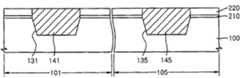
图2A-2F说明根据示范性实施例形成半导体器件的对准键的方法。参照图2A,在半导体衬底200上形成衬垫氧化层210和硬掩模层220。该硬掩模层220可以包括氮化物层等,可以根据待在随后工艺过程中形成的对准键的台阶高度差确定该硬掩模层220的厚度。可以刻蚀硬掩模层220和衬垫氧化物层210以暴露半导体衬底200的一部分。可以暴露其中形成单元元件的半导体衬底200中的芯片区域201的一部分和分离芯片区域201的划线道205的一部分。可以刻蚀半导体衬底200的暴露部分,从而在芯片区域201中形成第一沟槽231,并在划线道205中形成第二沟槽235。第一沟槽231可以形成限定芯片区域201的有源区的隔离层,第二沟槽235可以在划线道205中形成对准键。2A-2F illustrate a method of forming an alignment key of a semiconductor device according to an exemplary embodiment. Referring to FIG. 2A , a
参照图2B,在硬掩模层220上形成绝缘层240以填充第一沟槽231和第二沟槽235。绝缘层240可以由USG、O3-TEOS USG、和/或具有改善的间隙填充特性的高密度等离子体(HDP)氧化物层形成,以允许填充第一和第二沟槽231和235。Referring to FIG. 2B , an insulating
参照图2C,通过化学机械抛光(CMP)等刻蚀绝缘层240以平面化衬底表面。因而,隔离层241可以形成在第一沟槽231的内部,并且对准键245可以形成在第二沟槽235内部。在通过绝缘层240填充第一和第二沟槽231和235之前,由氮化物层形成的衬里、用于减轻衬里和衬底之间应力的作为氧化物缓冲层的热氧化层、和/或中间温度氧化物(MTO)层可以形成在第一和第二沟槽231和235内部。Referring to FIG. 2C, the insulating
参照图2D,可以使用磷酸剥离工艺等除去硬掩模层220和衬垫氧化物层210。隔离层241可以形成在衬底表面和隔离层241之间具有台阶高度差的衬底200的芯片区域201中,突出对准键245可以形成在衬底表面和对准键245之间具有台阶高度差H2的划线道205中。可以依据硬掩模层220的厚度、CMP工艺、和/或硬掩模的磷酸脱膜工艺确定对准键245的台阶高度差H2。对准键245可以具有大约50

参照图2E,可以在具有隔离层241和对准键245的衬底200上形成用于形成元件的层250。该至少一个形成层250可以由相对于隔离层241和对准键245具有刻蚀选择率例如湿法刻蚀选择率等的材料组成。Referring to FIG. 2E , a layer 250 for forming elements may be formed on the
该至少一个形成层250可以包括导电层或者绝缘层。导电层可以是多晶硅层等,绝缘层可以是氮化物层等。可以使用该至少一个形成层250以在芯片区域201中形成单元元件(未显示),并且可以使用用于形成栅和/或电容器的底电极的多晶硅层、和/或用于形成电容器的ONO介质层的氮化物层。另外,当栅绝缘层使用氮化物层时,栅绝缘层可以用于该至少一个形成层250。另外,该至少一个形成层250可以使用用于形成芯片区域201的单元元件的多个层。The at least one forming layer 250 may include a conductive layer or an insulating layer. The conductive layer may be a polysilicon layer or the like, and the insulating layer may be a nitride layer or the like. The at least one formation layer 250 can be used to form a cell element (not shown) in the
参照图2F,可以图案化该至少一个形成层250,从而在芯片区域201中形成用于单元元件的图案251,和在划线道205中形成覆盖层255以覆盖对准键245。因为可以构筑由相对于对准键245具有湿法刻蚀选择率的材料组成的覆盖层255以覆盖对准键245,所以覆盖层255延迟、或者防止对准键245的氧化物层在用于形成单元元件的随后湿法刻蚀工艺过程中被损耗。因而,可以通过覆盖层255保持在对准键245和衬底之间的台阶高度差H2。Referring to FIG. 2F , the at least one formation layer 250 may be patterned to form a pattern 251 for unit elements in the
根据示范性实施例,形成对准键的方法可以保持对准键的台阶高度差,即使没有额外的掩模形成工艺过程,因为覆盖形成在划线道205中的对准键245的覆盖层255可以与形成元件形成图案251以形成芯片区域201的单元元件同时形成。According to an exemplary embodiment, the method of forming the alignment key can maintain the step height difference of the alignment key even without an additional mask forming process because the capping layer 255 covering the
图3A-3F说明根据示范性实施例制造半导体器件的方法。在示范性实施例中,当使用多晶硅层作为该至少一个形成层在芯片区域形成栅和电容器的底电极时,可以在划线道中同时形成对准键的覆盖层。3A-3F illustrate a method of fabricating a semiconductor device according to an exemplary embodiment. In an exemplary embodiment, when the gate and the bottom electrode of the capacitor are formed in the chip region using the polysilicon layer as the at least one formation layer, the capping layer of the alignment key may be simultaneously formed in the scribe lane.
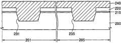
参照图3A,半导体衬底300可以包括其中形成单元元件的芯片区域302和分离芯片区域302的划线道305。可以在芯片区域302的第一区域301中形成MOS晶体管,可以在芯片区域302的第二区域303中形成电容器。可以通过与图2A-2D说明的相同的工艺过程刻蚀衬底300,从而在芯片区域302的第一区域301中形成第一沟槽311,在芯片区域302的第二区域303中形成第二沟槽313,和在划线道305中形成第三沟槽315。用绝缘层例如USG、O3-TEOS USG、和/或HDP氧化物层填充第一、第二和第三沟槽311、313、和315,可以执行CMP工艺等,从而在第一沟槽311和第二沟槽313中分别形成第一隔离层321和第二隔离层323。同时,可以在第三沟槽315中形成突出对准键325。Referring to FIG. 3A , a
参照图3B,可以在具有第一和第二隔离层321和323和形成于其上的对准键325的衬底上形成第一绝缘层330和多晶硅层340。可以通过沉积掺杂p型和/或n型杂质的多晶硅层,或者通过沉积未掺杂的多晶硅层并经离子注入工艺掺杂p型和/或n型杂质,来形成多晶硅层340。参照图3C,可以刻蚀多晶硅层340和第一绝缘层330,从而在第一区域301中形成具有栅氧化层331的栅341。可以在第二区域303中形成电容器的底电极343,覆盖层345可以由划线道305中的单晶硅层形成。第一绝缘层图案333和335可以分别保留在电容器的底电极343和覆盖层345下面。因而,当在芯片区域302中形成栅电极341和电容器底的电极343时,可以在划线道305中同时形成用于对准键325的覆盖层345。Referring to FIG. 3B , a first insulating
图3中的示范性实施例说明在芯片区域302中同时形成栅电极341和电容器的底电极343,但作为选择,可以沉积和图案化多晶硅层,从而在芯片区域302的第一区域301中形成栅341,可以沉积和图案化另一多晶硅层,从而在芯片区域302的第二区域303中形成电容器的底电极343。或者,可以在第二区域303中沉积和图案化多晶硅层,以便形成电容器的底电极343,可以在第一区域301中沉积和图案化多晶硅层,以便形成栅极。可以在形成栅的工艺过程和/或形成电容器的底部电极的工艺过程期间形成覆盖层345,可以在待执行的这些工艺过程的第一个的期间形成覆盖层345。The exemplary embodiment in FIG. 3 illustrates the simultaneous formation of the
示范性实施例还可以说明形成在芯片区域202中的一个晶体管,但是可以形成高压晶体管、中等电压晶体管、和/或低电压晶体管。在芯片区域中形成隔离层和在划线道中形成对准键之后,可以在芯片区域中形成厚的较高电压晶体管的栅绝缘层、中等电压晶体管的栅绝缘层、和/或薄的较低电压晶体管的栅绝缘层。当栅绝缘层由氮化物层形成时,并且同时形成栅绝缘层和覆盖层时,可以在无论从较高电压、中间电压、和/或较低电压晶体管中首先形成哪个栅氧化层的同时形成对准键的覆盖层。Exemplary embodiments may also illustrate one transistor formed in chip region 202 , but high voltage transistors, medium voltage transistors, and/or low voltage transistors may be formed. After the isolation layer is formed in the chip area and the alignment key is formed in the scribe lane, a thick gate insulating layer for higher voltage transistors, a gate insulating layer for medium voltage transistors, and/or a thin lower voltage transistor can be formed in the chip area. Gate insulating layer for voltage transistors. When the gate insulating layer is formed of a nitride layer, and the gate insulating layer and the capping layer are formed at the same time, it may be formed at the same time regardless of which gate oxide layer is formed first from among higher voltage, intermediate voltage, and/or lower voltage transistors. Align the overlay of the key.
参照图3D,可以在衬底上沉积第二绝缘层350。第二绝缘层350可以包括氧化物-氮化物-氧化物(ONO)层、氧化钽层、氧化锆层、氧化铪层、BST氧化物层、PZT和/或SBT氧化物层等的至少一个。参照图3E,可以图案化第二绝缘层350,从而在电容器的底电极343上形成电容器的介质层353。参照图3F,可以在衬底上沉积多晶硅层并对其图案化,从而在电容器的介质层353上形成电容器上电极363。当首先在形成栅341之前形成电容器的底电极343时,可以同时形成栅极341和电容器上电极363。Referring to FIG. 3D, a second insulating layer 350 may be deposited on the substrate. The second insulating layer 350 may include at least one of an oxide-nitride-oxide (ONO) layer, a tantalum oxide layer, a zirconium oxide layer, a hafnium oxide layer, a BST oxide layer, a PZT and/or an SBT oxide layer, and the like. Referring to FIG. 3E , the second insulating layer 350 may be patterned to form a
图4A-4D说明根据示范性实施例制造半导体器件的方法。图4A-4D,当使用多晶硅层和/或ONO层作为至少一个形成层在芯片区域中形成栅极、电容器的底电极、和电容器的介质层时,可在划线道中同时形成对准键的覆盖层。4A-4D illustrate a method of fabricating a semiconductor device according to an exemplary embodiment. 4A-4D, when using the polysilicon layer and/or the ONO layer as at least one formation layer to form the gate, the bottom electrode of the capacitor, and the dielectric layer of the capacitor in the chip area, the alignment keys can be formed simultaneously in the scribe lane overlay.
参照图4A,半导体衬底400可以包括其中将形成单元元件的芯片区域402、和分离芯片区域402的划线道405。可以在芯片区域402的第一区域401中形成MOS晶体管,可以在芯片区域402的第二区域403中形成电容器。与图3A中所述的示范性实施例相同,在芯片区域402的第一区域401和第二区域403中分别形成第一沟槽411和第二沟槽413,并可以在划线道405中形成第三沟槽415。在用氧化物层例如USG、O3-TEOS USG、和/或HDP氧化物层413填充第一、第二和第三沟槽411、413和415之后,可以执行CMP工艺等,从而分别在第一沟槽411、第二沟槽413中形成第一隔离层421和第二隔离层423。同时,可以在第三沟槽415中形成突出对准键425。Referring to FIG. 4A , a semiconductor substrate 400 may include a chip region 402 in which unit elements are to be formed, and a scribe line 405 separating the chip region 402 . A MOS transistor may be formed in a first region 401 of the chip region 402 , and a capacitor may be formed in a second region 403 of the chip region 402 . Same as the exemplary embodiment described in FIG. 3A, a first trench 411 and a second trench 413 are respectively formed in the first region 401 and the second region 403 of the chip region 402, and may be formed in the scribe line 405. A third trench 415 is formed. After filling the first, second, and third trenches 411, 413, and 415 with an oxide layer such as USG, O3-TEOS USG, and/or HDP oxide layer 413, a CMP process, etc., may be performed, respectively, in the first A first isolation layer 421 and a second isolation layer 423 are formed in the trench 411 and the second trench 413 . Meanwhile, a protrusion alignment key 425 may be formed in the third groove 415 .
参照图4B,可以在具有第一和第二隔离层421和423和对准键425的衬底上顺序地形成第一绝缘层430、多晶硅层440和第二绝缘层450。可以通过沉积掺杂p型和/或n型杂质的多晶硅层,或者通过沉积未掺杂的多晶硅层并经离子注入工艺掺杂p型和/或n型杂质形成多晶硅层440。第二绝缘层450可以至少包括氮化物层,例如,氧化物-氮化物-氧化物(ONO)层和/或NO层。Referring to FIG. 4B , a first insulating layer 430 , a polysilicon layer 440 and a second insulating layer 450 may be sequentially formed on the substrate having the first and second isolation layers 421 and 423 and the alignment key 425 . The polysilicon layer 440 may be formed by depositing a polysilicon layer doped with p-type and/or n-type impurities, or by depositing an undoped polysilicon layer and doping p-type and/or n-type impurities through an ion implantation process. The second insulating layer 450 may include at least a nitride layer, for example, an oxide-nitride-oxide (ONO) layer and/or an NO layer.
参照图4C,可以刻蚀多晶硅层440和第一和第二绝缘层430和450,从而在第一区域401中形成具有栅绝缘层431的栅极441。第二绝缘层图案451可以留在栅极441上。可以在第二区域403中形成电容器的底电极443和电容器的介质层453,并且可以在划线道405中形成覆盖层445a。覆盖层455a可以具有包括多晶硅层图案445和第二绝缘层图案455的堆叠结构。第一绝缘层图案433和435可以分别保留在电容器的底电极443和覆盖层445a下面。因而,当在芯片区域402中形成栅电极441和电容器的底电极443时,可以在划线道405中同时形成用于对准键425的覆盖层445a。Referring to FIG. 4C , the polysilicon layer 440 and the first and second insulating layers 430 and 450 may be etched, thereby forming a gate 441 having a gate insulating layer 431 in the first region 401 . The second insulating layer pattern 451 may remain on the gate electrode 441 . A capacitor's bottom electrode 443 and a capacitor's dielectric layer 453 may be formed in the second region 403 , and a capping layer 445 a may be formed in the scribe lane 405 . The capping layer 455 a may have a stack structure including a polysilicon layer pattern 445 and a second insulating layer pattern 455 . The first insulating layer patterns 433 and 435 may remain under the bottom electrode 443 and the capping layer 445a of the capacitor, respectively. Thus, when the gate electrode 441 and the bottom electrode 443 of the capacitor are formed in the chip region 402 , the capping layer 445 a for the alignment key 425 may be simultaneously formed in the scribe lane 405 .
图4中的示范性实施例说明同时形成在芯片区域402中的栅电极441和电容器的底电极443,但作为选择,可以沉积和图案化第一绝缘层和多晶硅层,以在芯片区域402的第一区域401中形成栅极441,可以沉积和图案化另一多晶硅层和第二绝缘层,以在芯片区域402的第二区域403中形成电容器的底电极443和电容器的介质层453。作为选择,可以在第二区域403中形成电容器的底电极443和电容器的介质层453之后,可以在第一区域401中形成栅极441。当形成栅极和/或电容器的底电极和电容器的介质层时可以形成覆盖层445a,并且可以在形成栅极和/或电容器的底电极和电容器的介质层的前面工艺过程中形成覆盖层445a。The exemplary embodiment in FIG. 4 illustrates that the gate electrode 441 and the bottom electrode 443 of the capacitor are simultaneously formed in the chip region 402, but alternatively, the first insulating layer and the polysilicon layer may be deposited and patterned to form the same in the chip region 402. A gate 441 is formed in the first region 401 , and another polysilicon layer and a second insulating layer may be deposited and patterned to form the bottom electrode 443 of the capacitor and the dielectric layer 453 of the capacitor in the second region 403 of the chip region 402 . Alternatively, the gate 441 may be formed in the first region 401 after the bottom electrode 443 of the capacitor and the dielectric layer 453 of the capacitor are formed in the second region 403 . The capping layer 445a may be formed when the gate and/or the bottom electrode of the capacitor and the dielectric layer of the capacitor are formed, and may be formed in a previous process of forming the gate and/or the bottom electrode of the capacitor and the dielectric layer of the capacitor .
参照图4D,在衬底上沉积多晶硅层并图案化之后,可以在电容器的介质层453上形成电容器上电极463。Referring to FIG. 4D, after depositing and patterning a polysilicon layer on the substrate, a capacitor upper electrode 463 may be formed on the dielectric layer 453 of the capacitor.
当在栅极441之前形成电容器的底电极443时,可以同时形成栅极441和电容器上电极463。在图4A至4D中所示的示范性实施例中,可以与图3A至3F所示的示范性实施例一样形成芯片区域402中的较高电压、中间电压、和/或较低电压晶体管。When the bottom electrode 443 of the capacitor is formed before the gate electrode 441, the gate electrode 441 and the capacitor upper electrode 463 may be formed simultaneously. In the exemplary embodiment shown in FIGS. 4A-4D , the higher voltage, intermediate voltage, and/or lower voltage transistors in chip region 402 may be formed as in the exemplary embodiment shown in FIGS. 3A-3F .
图5A-5F说明根据示范性实施例制造半导体器件的方法。在图5中,当使用氮化物层作为器件形成层在芯片区域中形成电容器的介质层时,可以在划线道中同时形成对准键的覆盖层。5A-5F illustrate a method of fabricating a semiconductor device according to an exemplary embodiment. In FIG. 5, when the dielectric layer of the capacitor is formed in the chip region using the nitride layer as the device formation layer, the capping layer of the alignment key can be simultaneously formed in the scribe lane.
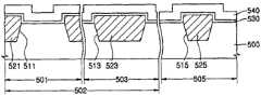
参照图5A,半导体衬底500可以包括其中形成单元元件的芯片区域502、和分离芯片区域502的划线道505。可以在芯片区域502的第一区域501中形成MOS晶体管,可以在芯片区域502的第二区域503中形成电容器。与图3A中的示范性实施例相同,蚀刻衬底500从而在芯片区域502的第一区域501和第二区域503中分别形成第一沟槽511和第二沟槽513,并可以在划线道505中形成第三沟槽515。在用绝缘层,例如,氧化物层例如USG、O3-TEOS USG、和/或HDP氧化物层填充第一、第二和第三沟槽511、513、和515之后,可以执行CMP工艺等,从而在第一沟槽511和第二沟槽513中分别形成第一隔离层521和第二隔离层523。同时,可以在第三沟槽515中形成突出对准键525。Referring to FIG. 5A , a
参照图5B,可以在具有第一和第二隔离层521和523和对准键525的衬底上形成第一绝缘层530和多晶硅层540。可以通过沉积掺杂p型和/或n型杂质的多晶硅层,或者通过沉积未掺杂的多晶硅层并经离子注入工艺掺杂p型和/或n型杂质形成多晶硅层540。参照图5C,可以刻蚀多晶硅层540和绝缘层530,从而在第一区域501中形成具有栅氧化层531的栅极541。可以在第二区域503中形成电容器的底电极543。第一绝缘层图案533可以留在电容器的底电极543下面。Referring to FIG. 5B , a first insulating
图5中的示范性实施例说明同时形成在芯片区域502中的栅电极541和电容器的底电极545,但可以通过沉积和图案化栅氧化层和多晶硅层在芯片区域502的第一区域501中形成栅极541,并且可以通过沉积和图案化另一多晶硅层在芯片区域502的第二区域503中形成电容器的底电极543。作为选择,可以在第二区域503中形成电容器的底电极543之后,可以在第一区域501中形成栅极541。The exemplary embodiment in FIG. 5 illustrates the simultaneous formation of the
参照图5D,可以在衬底上沉积第二绝缘层550。绝缘层550可以至少包括氮化物层,例如,ONO层和/或NO层。参照图5E,可以图案化第二绝缘层550,从而在电容器的底电极543上形成电容器的介质层553。可以在划线道505中同时形成用于对准键525的覆盖层555。因而,可以形成至少包括氮化物层的覆盖层555。参照图5F,可以在衬底上沉积多晶硅层并对其图案化,从而在电容器的介质层553上形成电容器上电极563。在图5A至5F所示的示范性实施例中,可以与图3A至3F所示的示范性实施例一样在芯片区域中形成较高电压、中间电压、和/或较低电压晶体管。Referring to FIG. 5D, a second insulating
如上详细地描述,根据示范性实施例,在划线区中形成相对于衬底具有台阶高度差的对准键之后,并且在芯片区域中形成元件形成图案之前,可以形成用于覆盖对准键的覆盖层。因此,因为额外的掩模形成工艺不是必需的,所以可以简化制造,并且覆盖层在随后的湿法刻蚀工艺过程中可以保护对准键,保持对准键的恒定台阶高度差,可以提高对准。As described above in detail, according to an exemplary embodiment, after an alignment key having a step height difference with respect to a substrate is formed in the scribe area and before an element formation pattern is formed in the chip area, an alignment key for covering may be formed. overlay. Therefore, since an additional mask forming process is not necessary, the manufacturing can be simplified, and the capping layer can protect the alignment keys during the subsequent wet etching process, maintain a constant step height difference of the alignment keys, and improve alignment. allow.
上文说明了示范性实施例并不认为是对其限制。在参照附图所示的示范性实施例具体显示和描述示范性实施例的同时,本领域的普通技术人员应当理解在不脱离权利要求的情况下可以进行方式和细节上的各种变化。The above describes exemplary embodiments and is not to be considered limiting. While exemplary embodiments are specifically shown and described with reference to the exemplary embodiments shown in the drawings, it will be understood by those skilled in the art that various changes in manner and details may be made without departing from the claims.
Claims (19)


Applications Claiming Priority (2)
| Application Number | Priority Date | Filing Date | Title |
|---|---|---|---|
| KR89476/05 | 2005-09-26 | ||
| KR1020050089476AKR100630768B1 (en) | 2005-09-26 | 2005-09-26 | Method for forming alignment key with capping layer and method for manufacturing semiconductor device using same |
Publications (2)
| Publication Number | Publication Date |
|---|---|
| CN1941281A CN1941281A (en) | 2007-04-04 |
| CN1941281Btrue CN1941281B (en) | 2011-02-09 |
Family
ID=37622756
Family Applications (1)
| Application Number | Title | Priority Date | Filing Date |
|---|---|---|---|
| CN2006101431876AActiveCN1941281B (en) | 2005-09-26 | 2006-09-26 | Method for forming alignment key of semiconductor device |
Country Status (5)
| Country | Link |
|---|---|
| US (1) | US7723203B2 (en) |
| JP (1) | JP2007096310A (en) |
| KR (1) | KR100630768B1 (en) |
| CN (1) | CN1941281B (en) |
| DE (1) | DE102006046425B4 (en) |
Families Citing this family (11)
| Publication number | Priority date | Publication date | Assignee | Title |
|---|---|---|---|---|
| KR100800680B1 (en)* | 2006-12-11 | 2008-02-01 | 동부일렉트로닉스 주식회사 | Method of forming interlayer insulating film of semiconductor device |
| KR100850859B1 (en)* | 2006-12-21 | 2008-08-06 | 동부일렉트로닉스 주식회사 | Image Sensor and The Fabricating Method thereof |
| US8119489B2 (en)* | 2008-03-28 | 2012-02-21 | United Microelectronics Corp. | Method of forming a shallow trench isolation structure having a polysilicon capping layer |
| US8013400B1 (en)* | 2008-04-21 | 2011-09-06 | National Semiconductor Corporation | Method and system for scaling channel length |
| JP5821174B2 (en)* | 2010-09-30 | 2015-11-24 | 富士通セミコンダクター株式会社 | Manufacturing method of semiconductor device |
| JP6174893B2 (en)* | 2013-04-16 | 2017-08-02 | ローム株式会社 | Semiconductor device and manufacturing method of semiconductor device |
| US9178066B2 (en)* | 2013-08-30 | 2015-11-03 | Taiwan Semiconductor Manufacturing Company Limited | Methods for forming a semiconductor arrangement with structures having different heights |
| KR102077150B1 (en) | 2013-09-16 | 2020-02-13 | 삼성전자주식회사 | Method for manufacturing semiconductor devices |
| KR102432776B1 (en)* | 2015-10-08 | 2022-08-17 | 에스케이하이닉스 주식회사 | Manufacturing method of semiconductor device |
| KR102563921B1 (en) | 2016-02-02 | 2023-08-04 | 삼성전자 주식회사 | Semiconductor Device |
| US11244907B2 (en) | 2020-01-02 | 2022-02-08 | International Business Machines Corporation | Metal surface preparation for increased alignment contrast |
Citations (4)
| Publication number | Priority date | Publication date | Assignee | Title |
|---|---|---|---|---|
| US5889335A (en)* | 1997-09-09 | 1999-03-30 | Mitsubishi Denki Kabushiki Kaisha | Semiconductor device and method of manufacturing the same |
| US6215197B1 (en)* | 1997-08-25 | 2001-04-10 | Mitsubishi Denki Kabushiki Kaisha | Semiconductor device having a trench isolation structure and an alignment mark area |
| US6440816B1 (en)* | 2001-01-30 | 2002-08-27 | Agere Systems Guardian Corp. | Alignment mark fabrication process to limit accumulation of errors in level to level overlay |
| US6706610B2 (en)* | 2000-03-09 | 2004-03-16 | Fujitsu Limited | Semiconductor device and fabrication process thereof |
Family Cites Families (9)
| Publication number | Priority date | Publication date | Assignee | Title |
|---|---|---|---|---|
| JPH10303096A (en) | 1997-04-23 | 1998-11-13 | Canon Inc | Method for manufacturing semiconductor device capable of protecting alignment mark |
| KR100248155B1 (en) | 1997-12-08 | 2000-03-15 | 김영환 | Method for forming align key of field region |
| JP3080070B2 (en) | 1998-06-12 | 2000-08-21 | 日本電気株式会社 | Semiconductor device and method of manufacturing semiconductor device |
| US6037236A (en) | 1998-08-17 | 2000-03-14 | Taiwan Semiconductor Manufacturing Company | Regeneration of alignment marks after shallow trench isolation with chemical mechanical polishing |
| JP2005150251A (en)* | 2003-11-12 | 2005-06-09 | Renesas Technology Corp | Manufacturing method of semiconductor device and semiconductor device |
| KR100593732B1 (en)* | 2003-11-18 | 2006-06-28 | 삼성전자주식회사 | A semiconductor device having an align key and a method of manufacturing the same |
| JP4439935B2 (en) | 2004-02-02 | 2010-03-24 | Okiセミコンダクタ株式会社 | Manufacturing method of semiconductor device |
| JP2006171344A (en)* | 2004-12-15 | 2006-06-29 | Nippon Sheet Glass Co Ltd | Optical film |
| KR100699860B1 (en)* | 2005-08-12 | 2007-03-27 | 삼성전자주식회사 | Method of forming alignment key in well structure forming process and device isolation formation method using same |
- 2005
- 2005-09-26KRKR1020050089476Apatent/KR100630768B1/enactiveActive
- 2006
- 2006-09-21USUS11/524,318patent/US7723203B2/enactiveActive
- 2006-09-22DEDE102006046425Apatent/DE102006046425B4/enactiveActive
- 2006-09-26JPJP2006260476Apatent/JP2007096310A/enactivePending
- 2006-09-26CNCN2006101431876Apatent/CN1941281B/enactiveActive
Patent Citations (4)
| Publication number | Priority date | Publication date | Assignee | Title |
|---|---|---|---|---|
| US6215197B1 (en)* | 1997-08-25 | 2001-04-10 | Mitsubishi Denki Kabushiki Kaisha | Semiconductor device having a trench isolation structure and an alignment mark area |
| US5889335A (en)* | 1997-09-09 | 1999-03-30 | Mitsubishi Denki Kabushiki Kaisha | Semiconductor device and method of manufacturing the same |
| US6706610B2 (en)* | 2000-03-09 | 2004-03-16 | Fujitsu Limited | Semiconductor device and fabrication process thereof |
| US6440816B1 (en)* | 2001-01-30 | 2002-08-27 | Agere Systems Guardian Corp. | Alignment mark fabrication process to limit accumulation of errors in level to level overlay |
Non-Patent Citations (1)
| Title |
|---|
| JP特开平11-354400A 1999.12.24 |
Also Published As
| Publication number | Publication date |
|---|---|
| KR100630768B1 (en) | 2006-10-04 |
| DE102006046425A1 (en) | 2007-06-06 |
| CN1941281A (en) | 2007-04-04 |
| US20070072386A1 (en) | 2007-03-29 |
| DE102006046425B4 (en) | 2011-03-03 |
| US7723203B2 (en) | 2010-05-25 |
| JP2007096310A (en) | 2007-04-12 |
Similar Documents
| Publication | Publication Date | Title |
|---|---|---|
| CN1941281B (en) | Method for forming alignment key of semiconductor device | |
| TWI695488B (en) | Non-volatile separation gate memory unit with integrated high-K metal control gate and manufacturing method thereof | |
| KR100635424B1 (en) | Nonvolatile semiconductor memory device and manufacturing method therof | |
| US12218209B2 (en) | Contacts for semiconductor devices and methods of forming the same | |
| TW202218093A (en) | Semiconductor device | |
| US20080179678A1 (en) | Two-sided semiconductor-on-insulator structures and methods of manufacturing the same | |
| US11901359B2 (en) | Method of manufacturing a semiconductor device | |
| US20050079661A1 (en) | Recessed gate transistor structure and method of forming the same | |
| US20060108644A1 (en) | Self-aligned double gate device and method for forming same | |
| US7211498B2 (en) | Method of manufacturing an isolation layer of a flash memory | |
| CN111106010B (en) | Transistor with stacked semiconductor layers as channel | |
| US8691703B2 (en) | Method of manufacturing semiconductor device | |
| CN107785377A (en) | The method for manufacturing semiconductor device | |
| CN100394586C (en) | Split gate flash device and method for manufacturing the same | |
| US10109638B1 (en) | Embedded non-volatile memory (NVM) on fully depleted silicon-on-insulator (FD-SOI) substrate | |
| JP2006344809A (en) | Semiconductor device and manufacturing method thereof | |
| US10580684B2 (en) | Self-aligned single diffusion break for fully depleted silicon-on-insulator and method for producing the same | |
| US20040245596A1 (en) | Semiconductor device having trench isolation | |
| US8617991B2 (en) | Method of manufacturing semiconductor device | |
| US8329519B2 (en) | Methods for fabricating a semiconductor device having decreased contact resistance | |
| US20040191992A1 (en) | Flash memory cell and fabrication thereof | |
| US20220416048A1 (en) | Semiconductor structure having stacked gates and method of manufacture thereof | |
| JP4823248B2 (en) | Nonvolatile semiconductor memory device and manufacturing method thereof | |
| CN116569340A (en) | Nanosheet semiconductor device with N/P boundary structure | |
| US20020187615A1 (en) | Method for forming isolations in memory devices with common source lines |
Legal Events
| Date | Code | Title | Description |
|---|---|---|---|
| C06 | Publication | ||
| PB01 | Publication | ||
| C10 | Entry into substantive examination | ||
| SE01 | Entry into force of request for substantive examination | ||
| C14 | Grant of patent or utility model | ||
| GR01 | Patent grant |