CN1937136B - Field-emitting cathode and plane light source - Google Patents
Field-emitting cathode and plane light sourceDownload PDFInfo
- Publication number
- CN1937136B CN1937136BCN2005100375107ACN200510037510ACN1937136BCN 1937136 BCN1937136 BCN 1937136BCN 2005100375107 ACN2005100375107 ACN 2005100375107ACN 200510037510 ACN200510037510 ACN 200510037510ACN 1937136 BCN1937136 BCN 1937136B
- Authority
- CN
- China
- Prior art keywords
- cathode
- light source
- layer
- getter material
- conductive layer
- Prior art date
- Legal status (The legal status is an assumption and is not a legal conclusion. Google has not performed a legal analysis and makes no representation as to the accuracy of the status listed.)
- Expired - Lifetime
Links
Images


Classifications
- H—ELECTRICITY
- H01—ELECTRIC ELEMENTS
- H01J—ELECTRIC DISCHARGE TUBES OR DISCHARGE LAMPS
- H01J61/00—Gas-discharge or vapour-discharge lamps
- H01J61/02—Details
- H01J61/30—Vessels; Containers
- H01J61/305—Flat vessels or containers
- B—PERFORMING OPERATIONS; TRANSPORTING
- B82—NANOTECHNOLOGY
- B82Y—SPECIFIC USES OR APPLICATIONS OF NANOSTRUCTURES; MEASUREMENT OR ANALYSIS OF NANOSTRUCTURES; MANUFACTURE OR TREATMENT OF NANOSTRUCTURES
- B82Y10/00—Nanotechnology for information processing, storage or transmission, e.g. quantum computing or single electron logic
- H—ELECTRICITY
- H01—ELECTRIC ELEMENTS
- H01J—ELECTRIC DISCHARGE TUBES OR DISCHARGE LAMPS
- H01J1/00—Details of electrodes, of magnetic control means, of screens, or of the mounting or spacing thereof, common to two or more basic types of discharge tubes or lamps
- H01J1/02—Main electrodes
- H01J1/30—Cold cathodes, e.g. field-emissive cathode
- H01J1/304—Field-emissive cathodes
- H—ELECTRICITY
- H01—ELECTRIC ELEMENTS
- H01J—ELECTRIC DISCHARGE TUBES OR DISCHARGE LAMPS
- H01J31/00—Cathode ray tubes; Electron beam tubes
- H01J31/08—Cathode ray tubes; Electron beam tubes having a screen on or from which an image or pattern is formed, picked up, converted, or stored
- H01J31/10—Image or pattern display tubes, i.e. having electrical input and optical output; Flying-spot tubes for scanning purposes
- H01J31/12—Image or pattern display tubes, i.e. having electrical input and optical output; Flying-spot tubes for scanning purposes with luminescent screen
- H01J31/123—Flat display tubes
- H01J31/125—Flat display tubes provided with control means permitting the electron beam to reach selected parts of the screen, e.g. digital selection
- H01J31/127—Flat display tubes provided with control means permitting the electron beam to reach selected parts of the screen, e.g. digital selection using large area or array sources, i.e. essentially a source for each pixel group
- H—ELECTRICITY
- H01—ELECTRIC ELEMENTS
- H01J—ELECTRIC DISCHARGE TUBES OR DISCHARGE LAMPS
- H01J61/00—Gas-discharge or vapour-discharge lamps
- H01J61/02—Details
- H01J61/24—Means for obtaining or maintaining the desired pressure within the vessel
- H01J61/26—Means for absorbing or adsorbing gas, e.g. by gettering; Means for preventing blackening of the envelope
- H—ELECTRICITY
- H01—ELECTRIC ELEMENTS
- H01J—ELECTRIC DISCHARGE TUBES OR DISCHARGE LAMPS
- H01J63/00—Cathode-ray or electron-stream lamps
- H01J63/06—Lamps with luminescent screen excited by the ray or stream
- H—ELECTRICITY
- H01—ELECTRIC ELEMENTS
- H01J—ELECTRIC DISCHARGE TUBES OR DISCHARGE LAMPS
- H01J2201/00—Electrodes common to discharge tubes
- H01J2201/30—Cold cathodes
- H01J2201/304—Field emission cathodes
- H01J2201/30446—Field emission cathodes characterised by the emitter material
- H01J2201/30453—Carbon types
- H01J2201/30469—Carbon nanotubes (CNTs)
Landscapes
- Engineering & Computer Science (AREA)
- Chemical & Material Sciences (AREA)
- Nanotechnology (AREA)
- Physics & Mathematics (AREA)
- Mathematical Physics (AREA)
- Theoretical Computer Science (AREA)
- Crystallography & Structural Chemistry (AREA)
- Vessels, Lead-In Wires, Accessory Apparatuses For Cathode-Ray Tubes (AREA)
- Discharge Lamp (AREA)
Abstract
Description
Translated fromChinese【技术领域】【Technical field】
本发明涉及一种场发射装置,尤其涉及一种场发射阴极及一种采用该场发射阴极的平面光源。The invention relates to a field emission device, in particular to a field emission cathode and a planar light source using the field emission cathode.
【背景技术】【Background technique】
碳纳米管(Carbon Nanotube,CNT)是一种新型碳材料,由日本研究人员Iijima在1991年发现,请参见″Helical Microtubules of Graphitic Carbon″,SIijima,Nature,vol.354,p56(1991)。碳纳米管是已知最好的场发射材料之一,其具有极低场发射电压,可传输极大电流密度,且电流极稳定,因而非常适合做场发射电子器件的电子发射源。目前碳纳米管最为热门的研究是平面显示方面的应用,例如应用在字符、图形及图像的显示。除此之外,在电光源领域,碳纳米管也具备潜在的应用前景,例如开发出应用在液晶显示器的背光源或照明用的光源。目前节能型高效光源多数利用水银,从环保角度看这是极为不利的,应当以其它光源取代之。因此利用碳纳米管的场发射特性制作光源是发展的趋势之一。Carbon Nanotube (Carbon Nanotube, CNT) is a new type of carbon material, discovered by Japanese researcher Iijima in 1991, see "Helical Microtubules of Graphic Carbon", SIijima, Nature, vol.354, p56 (1991). Carbon nanotubes are one of the best known field emission materials. They have extremely low field emission voltage, can transmit extremely high current density, and the current is extremely stable, so they are very suitable as electron emission sources for field emission electronic devices. At present, the most popular research on carbon nanotubes is the application of flat display, such as the display of characters, graphics and images. In addition, in the field of electric light sources, carbon nanotubes also have potential application prospects, such as the development of backlights for liquid crystal displays or light sources for lighting. At present, most energy-saving and high-efficiency light sources use mercury, which is extremely unfavorable from the perspective of environmental protection and should be replaced by other light sources. Therefore, it is one of the development trends to use the field emission characteristics of carbon nanotubes to make light sources.
碳纳米管平面光源的内部为一定的真空度。真空度是决定场发射稳定性的一个重要因素,如果碳纳米管阴极附近的真空度太低,将产生打火、气体电离、离子回轰阴极等问题,而将导致阴极发射电流的迅速衰减。因此,场发射阴极通常在高真空下才能稳定工作。The interior of the carbon nanotube planar light source is a certain degree of vacuum. The degree of vacuum is an important factor determining the stability of field emission. If the degree of vacuum near the carbon nanotube cathode is too low, problems such as ignition, gas ionization, and ion bombardment of the cathode will occur, which will lead to a rapid attenuation of the cathode emission current. Therefore, field emission cathodes usually work stably under high vacuum.
【发明内容】【Content of invention】
有鉴于此,有必要提供一种能有效保持一定真空度的场发射阴极及一种采用该场发射阴极的平面光源。In view of this, it is necessary to provide a field emission cathode capable of effectively maintaining a certain degree of vacuum and a planar light source using the field emission cathode.
一种场发射阴极,该场发射阴极包括一阴极导电层及一形成在所述阴极导电层上的电子发射体。其中,所述电子发射体为两层结构,吸气剂材料形成一吸气剂材料层,碳纳米管在所述吸气剂材料层上形成一碳纳米管层,该吸气剂材料层位于所述阴极导电层上。A field emission cathode includes a cathode conductive layer and an electron emitter formed on the cathode conductive layer. Wherein, the electron emitter has a two-layer structure, the getter material forms a getter material layer, and the carbon nanotubes form a carbon nanotube layer on the getter material layer, and the getter material layer is located on the on the cathode conductive layer.
一种平面光源,该平面光源包括一场发射阴极及一阳极。该场发射阴极包括一阴极导电层及一形成在所述阴极导电层上的电子发射体。该阳极包括一阳极导电层及一形成在所述阳极导电层上的荧光体层,该荧光体层和所述电子发射体相对,其中,所述电子发射体为两层结构,吸气剂材料形成一吸气剂材料层,碳纳米管在所述吸气剂材料层上形成一碳纳米管层,该吸气剂材料层位于所述阴极导电层上。A planar light source includes a field emission cathode and an anode. The field emission cathode includes a cathode conductive layer and an electron emitter formed on the cathode conductive layer. The anode includes an anode conductive layer and a phosphor layer formed on the anode conductive layer, the phosphor layer is opposite to the electron emitter, wherein the electron emitter has a two-layer structure, and the getter material A getter material layer is formed, and carbon nanotubes form a carbon nanotube layer on the getter material layer, and the getter material layer is located on the cathode conductive layer.
相较于现有技术,所述的场发射阴极,其电子发射体中含有吸气剂材料层,该吸气剂材料层能在场发射阴极工作过程中维持场发射阴极附近一定的真空度。采用所述场发射阴极的平面光源,光源阴极分布有吸气剂材料层,能维持平面光源内部真空度,以延长平面光源的工作寿命。Compared with the prior art, the electron emitter of the field emission cathode contains a getter material layer, and the getter material layer can maintain a certain degree of vacuum near the field emission cathode during the operation of the field emission cathode. In the planar light source using the field emission cathode, the cathode of the light source is distributed with a getter material layer, which can maintain the internal vacuum of the planar light source and prolong the working life of the planar light source.
【附图说明】【Description of drawings】
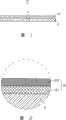
图1为本发明第一实施例提供的一种场发射阴极的截面示意图。FIG. 1 is a schematic cross-sectional view of a field emission cathode provided by the first embodiment of the present invention.
图2为图1中场发射阴极II部分的放大图。Fig. 2 is an enlarged view of part II of the field emission cathode in Fig. 1 .
图3为本发明第二实施例提供的一种场发射阴极的局部放大示意图。Fig. 3 is a partially enlarged schematic diagram of a field emission cathode provided by the second embodiment of the present invention.
图4为本发明第三实施例提供的一种场发射阴极的局部放大示意图。Fig. 4 is a partially enlarged schematic diagram of a field emission cathode provided by the third embodiment of the present invention.
图5为本发明第四实施例提供的一种采用第一、第二或第三实施例场发射阴极的平面光源的截面示意图。Fig. 5 is a schematic cross-sectional view of a planar light source using the field emission cathode of the first, second or third embodiment provided by the fourth embodiment of the present invention.
【具体实施方式】【Detailed ways】
以下将结合附图对本发明作进一步的详细说明。The present invention will be further described in detail below in conjunction with the accompanying drawings.
请一并参阅图1及图2,本发明第一实施例提供一种场发射阴极10,其包括一阴极导电层11及一电子发射体12。Please refer to FIG. 1 and FIG. 2 together. The first embodiment of the present invention provides a
电子发射体12为两层结构,吸气剂材料形成一吸气剂材料层121,碳纳米管在吸气剂材料层121上形成一碳纳米管层122,该吸气剂材料层121位于阴极导电层11上。碳纳米管122可通过化学气相沉积法、电弧放电法或激光蒸发法等现有方法制备,通过离心提纯得到纯度较高的碳纳米管,选取碳纳米管122的长度在5~15微米(μm)范围内为佳。阴极导电层11选用透明导电的氧化铟锡。吸气剂材料层121是非蒸散型吸气剂材料,非蒸散型吸气剂材料可选自钛、锆、钍、稀土金属或其合金。该吸气剂材料层121能在场发射阴极10工作过程中维持场发射阴极10附近一定的真空度。The
请参阅图3,本发明第二实施例提供一种场发射阴极20,其包括一阴极导电层21及一电子发射体22。电子发射体22位于阴极导电层21上,为单层结构。碳纳米管222呈阵列分布,吸气剂材料221分布在碳纳米管222阵列之间。吸气剂材料221是非蒸散型吸气剂材料,非蒸散型吸气剂材料可选自钛、锆、钍、稀土金属或其合金。Referring to FIG. 3 , the second embodiment of the present invention provides a field emission cathode 20 , which includes a cathode
请参阅图4,本发明第三实施例提供一种场发射阴极30,其包括一阴极导电层31及一电子发射体32。电子发射体32为单层结构,碳纳米管322及吸气剂材料321是混合分布。电子发射体32可采用丝网印刷方法制造。将碳纳米管322及吸气剂材料321混合成浆料后,涂覆在阴极导电层31上形成的。该方法简单,技术成熟,使制造成本降低,并有利于大规模生产。吸气剂材料321是非蒸散型吸气剂材料,非蒸散型吸气剂材料可选自钛、锆、钍、稀土金属或其合金。Please refer to FIG. 4 , the third embodiment of the present invention provides a
请参阅图5,本发明第四实施例提供一种平面光源1,其包括:一阴极基板2、一场发射阴极3、一阳极基板6、一阳极4及一边封体9。Referring to FIG. 5 , the fourth embodiment of the present invention provides a planar light source 1 , which includes: a
场发射阴极3形成在阴极基板2朝向平面光源1内部的表面上,采用的是本发明第一、第二或第三实施例提供的场发射阴极10、20或30,阴极基板2选用玻璃板。The field emission cathode 3 is formed on the surface of the
阳极4形成在阳极基板6朝向平面光源1内部的表面上,其包括一阳极导电层43及一荧光体层42,荧光体层42形成在阳极导电层43朝向平面光源1内部的表面上。荧光体层42选用高光电转换效率、低应用电压及长余辉的荧光体层为佳,荧光体层42的发光颜色可根据实际需要而定,可将平面光源1制作成照明用的白光光源或装饰用的彩色光源等。阳极基板6选用透明的玻璃板,阳极导电层43选用透明导电的氧化铟锡,这些都有利于光线的出射。The
为进一步提高平面光源1发光亮度,阳极4还包括一铝膜41,该铝膜41形成在荧光体层42朝向平面光源1内部的表面上。铝膜41的厚度约为50纳米(nm),当电子(图未示)高速从电子发射体射出,由于铝膜41很薄,电子很容易穿过,撞击荧光体层42而使荧光体层42发光形成亮点,此时铝膜41可将荧光体层42向平面光源1内部发射的光反射至平面光源1的外部,有利于提高亮点的亮度从而达到提高平面光源1发光亮度的目的。此外,铝膜41还有散热等其它作用。In order to further improve the luminance of the planar light source 1 , the
边封体9密封连接阴极基板2的边缘和阳极基板6的边缘,以形成一密封的空间。在阴极3与边封体9间及阳极4与边封体9间的间隙分别设有一吸气剂层8、5。本实施例中,位于阳极4与边封体9间的吸气剂层5成环状围绕阳极4,该吸气剂层5靠近荧光体层42,可迅速吸收荧光体层42在受到电子轰击时放出残留在荧光体层42中的气体,有效维持真空度。位于阴极3与边封体9间的吸气剂层8成环状围绕阴极,可进一步维持阴极3附近的真空度,以延长平面光源1的使用寿命。当然,阴极3与边封体9间及阳极4与边封体9间的吸气剂层8、5可设置于阴极3及阳极4的一边、二边或三边。The edge sealing body 9 seals and connects the edge of the
阴极基板2中设有一排气孔11,在对平面光源1进行抽真空作业时,该排气孔11可将气体从平面光源1内部排到外部。在平面光源1外部与阴极基板2中设有排气孔11的对应部位设有一密封装置12,使外部气体不得进入平面光源1内部。An
另外,因平面光源1内部为一定的真空环境,为确保各种尺寸的光源能承受外部大气压力并安全工作,在平面光源1内部设有多个支撑条10,支撑条10的数量视实际需要而定,支撑条10的材料选用透明、坚固的材料为佳。In addition, because the inside of the planar light source 1 is a certain vacuum environment, in order to ensure that light sources of various sizes can withstand external atmospheric pressure and work safely, a plurality of support bars 10 are arranged inside the planar light source 1, and the number of support bars 10 depends on actual needs Depending on the situation, the material of the
本实施例所提供的场发射阴极10、20、30,其电子发射体12、22、32中含有吸气剂材料121、221、321,该吸气剂材料121、221、321能在场发射阴极10、20、30工作过程中维持场发射阴极10、20、30附近一定的真空度。采用该场发射阴极10、20、30的平面光源1,其内部阴极3与边封体9及阳极4与边封体9间分别设有吸气剂层8、5,吸气剂层5靠近荧光体层42,可迅速吸收荧光体层42在受到电子轰击时放出残留在荧光体层42中的气体。吸气剂材料分布广,能进一步维持平面光源1内部真空度,以及延长平面光源1的工作寿命。
另外,本领域技术人员还可在本发明精神内做其它变化。当然,这些依据本发明精神所做的变化,都应包含在本发明所要求保护的范围之内。In addition, those skilled in the art can also make other changes within the spirit of the present invention. Of course, these changes made according to the spirit of the present invention should all be included within the scope of protection claimed by the present invention.
Claims (7)
Priority Applications (2)
| Application Number | Priority Date | Filing Date | Title |
|---|---|---|---|
| CN2005100375107ACN1937136B (en) | 2005-09-22 | 2005-09-22 | Field-emitting cathode and plane light source |
| US11/438,010US7812513B2 (en) | 2005-09-22 | 2006-05-19 | Field emission cathode and planar light source using the same |
Applications Claiming Priority (1)
| Application Number | Priority Date | Filing Date | Title |
|---|---|---|---|
| CN2005100375107ACN1937136B (en) | 2005-09-22 | 2005-09-22 | Field-emitting cathode and plane light source |
Publications (2)
| Publication Number | Publication Date |
|---|---|
| CN1937136A CN1937136A (en) | 2007-03-28 |
| CN1937136Btrue CN1937136B (en) | 2011-01-05 |
Family
ID=37883390
Family Applications (1)
| Application Number | Title | Priority Date | Filing Date |
|---|---|---|---|
| CN2005100375107AExpired - LifetimeCN1937136B (en) | 2005-09-22 | 2005-09-22 | Field-emitting cathode and plane light source |
Country Status (2)
| Country | Link |
|---|---|
| US (1) | US7812513B2 (en) |
| CN (1) | CN1937136B (en) |
Families Citing this family (11)
| Publication number | Priority date | Publication date | Assignee | Title |
|---|---|---|---|---|
| CN100555530C (en)* | 2006-03-24 | 2009-10-28 | 清华大学 | Field emission double-faced display light source and manufacture method thereof |
| CN100573797C (en)* | 2006-07-05 | 2009-12-23 | 清华大学 | The field emission pixel tube of double-side |
| US7635945B2 (en)* | 2006-07-21 | 2009-12-22 | Tsinghua University | Field emission device having a hollow shaped shielding structure |
| CN102403188A (en)* | 2010-09-08 | 2012-04-04 | 海洋王照明科技股份有限公司 | Field emission planar light source and preparation method thereof |
| CN103775909A (en)* | 2012-10-24 | 2014-05-07 | 海洋王照明科技股份有限公司 | Underground lamp |
| CN103838441B (en)* | 2012-11-23 | 2016-09-28 | 北京富纳特创新科技有限公司 | Capacitive touch screen |
| EP3511974B1 (en)* | 2014-12-17 | 2021-02-24 | LightLab Sweden AB | Field emission light source |
| US10175005B2 (en)* | 2015-03-30 | 2019-01-08 | Infinera Corporation | Low-cost nano-heat pipe |
| SE1750878A1 (en)* | 2017-07-05 | 2018-11-20 | Lightlab Sweden Ab | A field emission cathode structure for a field emission arrangement |
| NL2020465B1 (en)* | 2018-02-20 | 2019-08-29 | Univ Delft Tech | Apparatus and method for inspecting a surface of a sample, using a multi-beam charged particle column |
| US10395887B1 (en) | 2018-02-20 | 2019-08-27 | Technische Universiteit Delft | Apparatus and method for inspecting a surface of a sample, using a multi-beam charged particle column |
Citations (1)
| Publication number | Priority date | Publication date | Assignee | Title |
|---|---|---|---|---|
| US6741019B1 (en)* | 1999-10-18 | 2004-05-25 | Agere Systems, Inc. | Article comprising aligned nanowires |
Family Cites Families (8)
| Publication number | Priority date | Publication date | Assignee | Title |
|---|---|---|---|---|
| US5578900A (en)* | 1995-11-01 | 1996-11-26 | Industrial Technology Research Institute | Built in ion pump for field emission display |
| US5866978A (en)* | 1997-09-30 | 1999-02-02 | Fed Corporation | Matrix getter for residual gas in vacuum sealed panels |
| US6630772B1 (en)* | 1998-09-21 | 2003-10-07 | Agere Systems Inc. | Device comprising carbon nanotube field emitter structure and process for forming device |
| BR0001211C1 (en)* | 2000-04-13 | 2002-03-05 | Inst Nac De Tecnologia Da Info | Sending plate structure for fed |
| JP3768908B2 (en)* | 2001-03-27 | 2006-04-19 | キヤノン株式会社 | Electron emitting device, electron source, image forming apparatus |
| JP2003303541A (en) | 2002-04-11 | 2003-10-24 | Sony Corp | Ink for field electron emission electrode, and manufacturing method of field electron emission film, field electron emission electrode, and field electron emission display device using ink |
| JP2003303540A (en)* | 2002-04-11 | 2003-10-24 | Sony Corp | Field electron emission membrane, field electron emission electrode, and field electron emission display device |
| US7157848B2 (en)* | 2003-06-06 | 2007-01-02 | Electrovac Fabrikation Elektrotechnischer Spezialartikel Gmbh | Field emission backlight for liquid crystal television |
- 2005
- 2005-09-22CNCN2005100375107Apatent/CN1937136B/ennot_activeExpired - Lifetime
- 2006
- 2006-05-19USUS11/438,010patent/US7812513B2/enactiveActive
Patent Citations (1)
| Publication number | Priority date | Publication date | Assignee | Title |
|---|---|---|---|---|
| US6741019B1 (en)* | 1999-10-18 | 2004-05-25 | Agere Systems, Inc. | Article comprising aligned nanowires |
Also Published As
| Publication number | Publication date |
|---|---|
| US20070063630A1 (en) | 2007-03-22 |
| US7812513B2 (en) | 2010-10-12 |
| CN1937136A (en) | 2007-03-28 |
Similar Documents
| Publication | Publication Date | Title |
|---|---|---|
| JP4481948B2 (en) | Field emitter cathode, method of manufacturing the same, and planar light source | |
| CN101097829A (en) | Diode field emission pixel tube | |
| TW201241861A (en) | Double-sided light emitting field emission device and manufacturing method thereof | |
| CN1937136B (en) | Field-emitting cathode and plane light source | |
| CN101471224A (en) | Double-side light-emitting surface light source device | |
| JP2008153228A (en) | ELECTRON EMITTING LIGHT EMITTING DEVICE AND LIGHT EMITTING METHOD THEREOF | |
| CN101246804A (en) | Electron emission type light emitting element and light emitting method thereof | |
| CN101211748B (en) | Light source device | |
| JP4036572B2 (en) | Manufacturing method of electron emission source | |
| CN101042982A (en) | Field emission displaying light source and method of making same | |
| US8786171B2 (en) | Field emission light source device and manufacturing method thereof | |
| CN102333393B (en) | Field emission illumination light source | |
| JP5625113B2 (en) | Field emission surface light source and manufacturing method thereof | |
| CN1941263B (en) | Field-transmitting display device | |
| JP2008147193A (en) | Field emission lamp | |
| KR20050077539A (en) | Field emission type backlight unit for lcd | |
| CN101819915A (en) | Split joint type large-area field emission planar light source | |
| JP2011165678A (en) | Surface light source device with both faces emitting light | |
| JP2007066894A (en) | Anode element and field emission display using the anode element | |
| CN1728330A (en) | Field Emission Luminescence Lighting Source | |
| CN2731902Y (en) | Field emitting luminous illumination light source | |
| TWI303075B (en) | Field emission double planes light source and method for making the same | |
| CN202084504U (en) | shadow mask plasma display panel | |
| TWI310574B (en) | Field emission cathode and plane light source | |
| JP2008153222A (en) | Field emission lamp |
Legal Events
| Date | Code | Title | Description |
|---|---|---|---|
| C06 | Publication | ||
| PB01 | Publication | ||
| C10 | Entry into substantive examination | ||
| SE01 | Entry into force of request for substantive examination | ||
| C14 | Grant of patent or utility model | ||
| GR01 | Patent grant | ||
| CI01 | Publication of corrected invention patent application | Correction item:Patentee|Address|Co-patentee Correct:Tsinghua University|Hung Fujin Precision Industrial (Shenzhen) Co., Ltd. False:Hongfujin Precision Industry (Shenzhen) Co., Ltd.|518109 Guangdong city of Shenzhen province Baoan District Longhua Town Industrial Zone tabulaeformis tenth East Ring Road No. 2 two Number:01 Volume:27 | |
| CI03 | Correction of invention patent | Correction item:Patentee|Address|Co-patentee Correct:Tsinghua University|100084 Department of Tsinghua University, Tsinghua University, Tsinghua University, Tsinghua University, Beijing, China|HONG FU JIN PRECISION INDUSTRY (SHENZHEN) Co.,Ltd. False:HONG FU JIN PRECISION INDUSTRY (SHENZHEN) Co.,Ltd.|Guangdong province Shenzhen city Baoan District town Longhua tenth Industrial Zone tabulaeformis East Ring Road No. 2 two Number:01 Page:The title page Volume:27 Correction item:Patentee|Address|Co-patentee Correct:Tsinghua University|Hung Fujin Precision Industrial (Shenzhen) Co., Ltd. False:Hongfujin Precision Industry (Shenzhen) Co., Ltd.|518109 Guangdong city of Shenzhen province Baoan District Longhua Town Industrial Zone tabulaeformis tenth East Ring Road No. 2 two Number:01 Page:The title page Volume:27 | |
| ERR | Gazette correction | Free format text:CORRECT: PATENTEE; ADDRESS; CO-PATENTEE; FROM: HONGFUJIN PRECISION INDUSTRY (SHENZHEN) CO., LTD.;518109 NO. 2, EAST RING ROAD 2, YOUSONG INDUSTRIAL AREA 10, LONGHUA TOWN, BAOAN DISTRICT, SHENZHEN CITY, GUANGDONG PROVINCE TO: TSINGHUA UNIVERSITY;100084 DEPARTMENT OF PHYSICS, TSINGHUA UNIVERSITY, HAIDIAN DISTRICT, BEIJING; HONGFUJIN PRECISION INDUSTRY (SHENZHEN) CO., LTD. | |
| CX01 | Expiry of patent term | Granted publication date:20110105 |