CN1932783A - Memory control apparatus - Google Patents
Memory control apparatusDownload PDFInfo
- Publication number
- CN1932783A CN1932783ACNA2006101534891ACN200610153489ACN1932783ACN 1932783 ACN1932783 ACN 1932783ACN A2006101534891 ACNA2006101534891 ACN A2006101534891ACN 200610153489 ACN200610153489 ACN 200610153489ACN 1932783 ACN1932783 ACN 1932783A
- Authority
- CN
- China
- Prior art keywords
- access
- mentioned
- buffer
- external memory
- address
- Prior art date
- Legal status (The legal status is an assumption and is not a legal conclusion. Google has not performed a legal analysis and makes no representation as to the accuracy of the status listed.)
- Pending
Links
Images


Classifications
- G—PHYSICS
- G06—COMPUTING OR CALCULATING; COUNTING
- G06F—ELECTRIC DIGITAL DATA PROCESSING
- G06F13/00—Interconnection of, or transfer of information or other signals between, memories, input/output devices or central processing units
- G06F13/14—Handling requests for interconnection or transfer
- G06F13/16—Handling requests for interconnection or transfer for access to memory bus
- G06F13/1605—Handling requests for interconnection or transfer for access to memory bus based on arbitration
- G06F13/161—Handling requests for interconnection or transfer for access to memory bus based on arbitration with latency improvement
- G06F13/1626—Handling requests for interconnection or transfer for access to memory bus based on arbitration with latency improvement by reordering requests
- G06F13/1631—Handling requests for interconnection or transfer for access to memory bus based on arbitration with latency improvement by reordering requests through address comparison
Landscapes
- Engineering & Computer Science (AREA)
- Theoretical Computer Science (AREA)
- Physics & Mathematics (AREA)
- General Engineering & Computer Science (AREA)
- General Physics & Mathematics (AREA)
- Storage Device Security (AREA)
- Memory System (AREA)
Abstract
Translated fromChinese
Description
Translated fromChinese技术区域technology area
本发明涉及多个主板共有外部存储器上的数据并进行主板和外部存储器间的数据传送的存储器控制装置。The invention relates to a memory control device for sharing data on an external memory by a plurality of main boards and performing data transmission between the main board and the external memory.
背景技术Background technique
过去,在存储器控制装置中采用了以下技术,即,当对外部存储器进行存取的接口的存取单位比主板的存取单位大时,为了有效地进行外部存储器的读取,设置外部存储器侧的相当于存取单位的数据缓冲器,预先从外部存储器读取数据缓冲器单位的数据进行保存,并且,在连续发生单位地址区域内的读访问(read access)时,不访问外部存储器,而是从数据缓冲器读取。在此,当特定的主板读取由其它主板重写的外部存储器上的数据时,由于数据缓冲器和外部存储器之间不一定匹配,需要对数据缓冲进行无效化。In the past, the following technology has been adopted in the memory control device, that is, when the access unit of the interface for accessing the external memory is larger than the access unit of the motherboard, in order to efficiently read the external memory, the external memory side is provided. In the data buffer corresponding to the access unit, the data of the data buffer unit is read from the external memory in advance and stored, and when read access (read access) in the unit address area occurs consecutively, the external memory is not accessed, but the external memory is not accessed. is read from the data buffer. Here, when a specific motherboard reads data on the external memory rewritten by other motherboards, the data buffer needs to be invalidated because the data buffer does not necessarily match the external memory.
还公开了如下技术,即,为了减少由该无效化存取引起的主板的存取次数,将数据缓冲器的一部分地址(例如16字节边界的每个数据块的、例如开始地址和结束地址)作为特定地址,如果检测出从主板对特定地址的读取,则缓冲器控制装置同时进行数据缓冲器的无效化和从外部存储器的相当于存取单位的读取(参照专利文献1)。It also discloses the following technology, that is, in order to reduce the number of accesses of the main board caused by the invalidation access, a part of the address of the data buffer (for example, the start address and the end address of each data block on the 16-byte boundary) ) as a specific address, if reading of the specific address from the motherboard is detected, the buffer control device simultaneously invalidates the data buffer and reads the corresponding access unit from the external memory (see Patent Document 1).
专利文献1:日本特开平6-243037号公报(第6页、图1)Patent Document 1: Japanese Patent Application Laid-Open No. 6-243037 (page 6, FIG. 1 )
在上述公报公开的装置中,当从主板的存取随机进行时,如果发生对作为数据缓冲器的一部分地址的特定地址的读取,数据缓冲器一定被无效化,所以,存在数据缓冲器的命中率降低、对外部存储器的存取效率恶化的课题。In the device disclosed in the above publication, when the access from the main board is performed randomly, if a specific address as a part of the address of the data buffer is read, the data buffer must be invalidated. Hit rate reduction, deterioration of access efficiency to external memory issues.
而且,当发生了对数据缓冲器进行无效化的必要时,以前执行作为假存取(dummy access)请求发行对外部存储器上的其它地址区域的存取请求的方法,但是,存在为了发出对外部存储器的存取请求而需要多余的存取时间的课题。Moreover, when it is necessary to invalidate the data buffer, a method of issuing an access request to another address area on the external memory as a dummy access request has been previously performed, but there is a method for issuing an access request to the external memory The problem that extra access time is required for memory access requests.
此外,在主板间不进行排他控制的比较简单的系统中,特定的主板为了检测位于外部存储器上的系统状态被其它主板重写的情况,对特定的地址进行轮询存取时,因重复进行对相同地址的读取,数据缓冲器连续被命中,存在不能取得与外部存储器的匹配性的课题,上述公报没有公开其解决方法。In addition, in a relatively simple system that does not perform exclusive control between main boards, when a specific main board performs polling access to a specific address in order to detect that the system state on the external memory has been rewritten by other main boards, due to repeated For reading from the same address, the data buffer is continuously hit, and there is a problem that compatibility with the external memory cannot be obtained, and the above-mentioned publication does not disclose a solution to this problem.
发明内容Contents of the invention
本发明是鉴于上述问题而做出的,其目的在于提供一种存储器控制装置,抑制对外部存储器的存取效率的恶化,同时能够可靠地获得与外部存储器的匹配性。The present invention has been made in view of the above problems, and an object of the present invention is to provide a memory control device capable of reliably obtaining compatibility with the external memory while suppressing deterioration of access efficiency to the external memory.
为了解决上述课题,本发明的存储器控制装置是,进行主板和外部存储器间的数据传送的存储器控制装置,其具备:主板接口,接受来自上述主板的存取请求,输出对上述外部存储器的存取请求;以及外部存储器接口,接受来自上述主板接口的存取请求,进行对上述外部存储器的存取;上述主板接口具备:数据缓冲器,在请求存取时保存从上述外部存储器接口传送的数据;地址缓冲器,保存上述请求存取的地址;第1比较单元,比较新请求存取的地址和被保存在上述地址缓冲器中的地址,输出表示在被保存在上述数据缓冲器中的数据的地址范围内是否一致的第1比较信息;缓冲器控制单元,在上述第1比较信息表示不一致时,对上述外部存储器接口发行上述存取请求,在上述第1比较信息表示一致时,不对上述外部存储器接口发行上述存取请求,而是从上述数据缓冲器对主板进行数据输出;以及特定存取检测单元,当检测出上述存取请求是从上述主板对上述外部存储器上的特定地址的存取请求时,同上述第1比较信息是表示一致还是不一致无关地,判别对上述外部存储器接口是否发行上述存取请求,控制上述缓冲器控制单元。In order to solve the above-mentioned problems, the memory control device of the present invention is a memory control device that performs data transfer between a main board and an external memory, and includes a main board interface that receives an access request from the main board and outputs an access request to the external memory. request; and an external memory interface, accepting an access request from the above-mentioned mainboard interface, and performing access to the above-mentioned external memory; the above-mentioned mainboard interface has: a data buffer, which stores the data transmitted from the above-mentioned external memory interface when requesting access; The address buffer saves the address of the above-mentioned request for access; the 1st comparison unit compares the address of the new request for access with the address stored in the above-mentioned address buffer, and the output represents the data stored in the above-mentioned data buffer The first comparison information of whether the address range is consistent or not; the buffer control unit, when the first comparison information indicates inconsistency, issues the above-mentioned access request to the external memory interface; The memory interface issues the above-mentioned access request, but outputs data from the above-mentioned data buffer to the main board; and the specific access detection unit, when detecting that the above-mentioned access request is from the above-mentioned main board to the specific address on the above-mentioned external memory When requesting, regardless of whether the first comparison information indicates match or inconsistency, it is judged whether or not the access request is issued to the external memory interface, and the buffer control unit is controlled.
而且,也可以是,上述特定存取检测单元具备:第2比较单元,比较上述新请求存取的地址和上述外部存储器上的特定地址,向上述缓冲器控制单元输出表示是否一致的第二比较信息;以及无效化单元,在上述第2比较信息表示一致时,控制上述缓冲器控制单元,以便对上述地址缓冲器的内容进行无效化,并虚拟地进行存取响应。Furthermore, the specific access detection unit may include: a second comparison unit that compares the address newly requested for access with a specific address on the external memory, and outputs a second comparison indicating whether they match to the buffer control unit. information; and invalidation means for controlling the buffer control means to invalidate the content of the address buffer and virtually perform an access response when the second comparison information indicates a match.
而且,也可以是,上述特定地址是,外部存储器接口为了在存取控制时使用,禁止进行来自上述主板的存取的外部存储器上的特定区域的一部分地址。Furthermore, the specific address may be a part of addresses in a specific area on the external memory to which access from the main board is prohibited for use by the external memory interface at the time of access control.
而且,也可以是,上述特定存取检测单元还具备可以任意设定特定地址的特定地址设定寄存器。Furthermore, the specific access detection unit may further include a specific address setting register in which a specific address can be set arbitrarily.
而且,也可以是,上述存储器控制装置还具备假存取发行单元,该假存取发行单元接受表示上述外部存储器上的共有数据已被更新的通知,向上述主板接口发行对上述特定的地址的存取请求。Furthermore, the above-mentioned memory control device may further include a dummy access issuing unit that receives a notification indicating that the shared data on the above-mentioned external memory has been updated, and issues a notification to the above-mentioned specific address to the above-mentioned motherboard interface. access request.
而且,也可以是,上述特定存取检测单元同上述第1比较信息是否表示一致和不一致的任一个无关地,根据上述新请求存取的地址和过去请求存取的地址之间的比较,控制上述缓冲器控制单元,使得强制地发行或禁止对上述外部存储器接口的存取请求。Moreover, it is also possible that the above-mentioned specific access detecting unit controls whether or not the above-mentioned first comparison information indicates any of coincidence or inconsistency, based on a comparison between the address of the new request for access and the address of the past request for access. The buffer control unit forcibly issues or prohibits an access request to the external memory interface.
而且,也可以是,上述特定存取检测单元具备:缓冲器存取历史保存单元,保存表示来自上述主板的存取请求是对上述外部存储器接口的存取请求、还是对上述数据缓冲器的存取请求的历史信息;第3比较单元,比较上述新请求存取的地址和被保存在上述地址缓冲器的地址,向缓冲器更新单元输出表示是否完全一致的第3比较信息;以及缓冲器更新单元,在上述第3比较信息表示一致、上述缓冲器存取历史保存单元的历史信息表示对上述数据缓冲器的存取请求时,控制上述缓冲器控制单元,使得强制地对上述外部存储器接口发行存取请求。Furthermore, the specific access detection unit may include: a buffer access history storage unit that stores whether the access request from the main board is an access request to the external memory interface or a storage to the data buffer. Get the history information of request; The 3rd comparison unit compares the address of the above-mentioned new request access and the address stored in the above-mentioned address buffer, and outputs the 3rd comparison information indicating whether it is completely consistent to the buffer update unit; and the buffer update A means for controlling the buffer control means to forcibly issue data to the external memory interface when the third comparison information indicates a match and the history information of the buffer access history storage means indicates an access request to the data buffer. access request.
而且,也可以是,上述存储器控制装置还具备假存取发行单元,该假存取发行单元接受表示上述外部存储器上的共有数据已被更新的通知,向上述主板接口发行对被保存在上述地址缓冲器的地址的存取请求。Furthermore, the above-mentioned memory control device may further include a dummy access issuing unit, which receives a notification indicating that the shared data on the above-mentioned external memory has been updated, and issues to the above-mentioned main board interface the information stored at the above-mentioned address. An access request for the address of the buffer.
而且,也可以是,上述主板是DMA(直接存储器存取)控制器;上述通知表示上述直接存储器存取控制器的启动请求;当上述假存取发行单元接受到上述通知时,控制上述直接存储器存取控制器,使得在上述存取请求的发行之后开始数据传送。And, also can be, above-mentioned mainboard is DMA (direct memory access) controller; Above-mentioned notice represents the starting request of above-mentioned direct memory access controller; The access controller starts data transfer after the above-mentioned issuance of the access request.
而且,也可以是,上述直接存储器存取控制器具备多个通道;上述通知表示上述多个通道的一个的启动请求;上述存储器控制装置还具备按每个上述通道设定为允许及禁止的某一个值的假存取控制寄存器;对于通过上述通知请求了启动的通道,在上述假存取控制寄存器的值被设定为禁止时,上述假存取发行单元禁止上述存取请求的发行。Furthermore, the direct memory access controller may be provided with a plurality of channels; the notification may indicate an activation request for one of the plurality of channels; A dummy access control register of a value; for a channel that has been requested to be enabled through the notification, when the value of the dummy access control register is set to prohibit, the dummy access issuing unit prohibits issuance of the access request.
而且,也可以是,上述直接存储器存取控制器具备多个通道;上述通知将上述多个通道的一个的启动请求和启动要因一起表示;上述存储器控制装置还具备假存取控制寄存器,该假存取控制寄存器按每个启动要因设定为允许及禁止的某一个值,并且由各通道共用;对于由上述通知表示的启动要因,在上述假存取控制寄存器的值被设定为禁止时,上述假存取发行单元禁止上述存取请求的发行。Furthermore, the direct memory access controller may have a plurality of channels; the notification may indicate an activation request of one of the plurality of channels together with an activation factor; and the memory control device may further include a dummy access control register, and the dummy The access control register is set to a certain value of permission and prohibition for each activation factor, and is shared by each channel; for the activation factor indicated by the above notification, when the value of the above false access control register is set to prohibition , the above-mentioned fake access issuing unit prohibits the above-mentioned issuance of the access request.
而且,也可以是,上述特定存取检测单元具备:存取历史缓冲器,保存至少包含上述过去请求存取的地址的存取信息;第4比较单元,比较至少包含上述新请求存取的地址的新存取信息和被保存在上述存取历史缓冲器的存取信息,输出同一存取是否重复进行的第4比较信息;以及缓冲器无效化单元,在上述第4比较信息表示重复存取时,控制上述缓冲器控制单元,使得对上述外部存储器接口强制地发行存取请求。Moreover, it is also possible that the above-mentioned specific access detection unit includes: an access history buffer, storing access information including at least the address of the above-mentioned past request for access; The new access information and the access information stored in the above-mentioned access history buffer output the 4th comparison information of whether the same access is repeated; , the buffer control unit is controlled such that an access request is forcibly issued to the external memory interface.
而且,也可以是,上述缓冲器无效化单元在控制缓冲器控制单元,以便对外部存储器接口发行存取请求时,当上述第4比较信息表示重复存取时,控制成发行请求在上述新的存取请求中表示的请求大小的数据的存取请求,当上述第4比较信息表示不是重复存取时,控制成发行请求上述数据缓冲器大小的数据的存取请求。Furthermore, when the buffer invalidation unit controls the buffer control unit so as to issue an access request to the external memory interface, when the fourth comparison information indicates repeated access, it may be controlled so that the request is issued in the new memory interface. An access request for data of the requested size indicated in the access request is controlled to issue an access request requesting data of the size of the data buffer when the fourth comparison information indicates that it is not repeated access.
而且,也可以是,上述存储器控制装置还具备缓冲器更新单元,在上述第4比较信息表示重复存取时,上述缓冲器更新单元用从上述外部存储器接口读取的数据更新上述数据缓冲器的内容。In addition, the memory control device may further include a buffer update unit configured to update the data in the data buffer with the data read from the external memory interface when the fourth comparison information indicates repeated access. content.
而且,也可以是,上述外部存储器接口具备:轮询地址设定寄存器,可以任意设定上述外部存储器上的地址;轮询存取历史保存单元,通过对被设定在上述轮询地址设定寄存器中的地址的读访问进行设置,通过写访问进行复位;以及外部存储器选择单元,当发生了从上述主板接口对被设定在上述轮询地址设定寄存器的地址的读访问请求时,如果上述轮询存取历史保存单元被设置,则禁止对上述外部存储器的存取,在同对上述外部存储器进行存取时相比在短时间内,向上述主板接口响应;上述特定存取检测单元还具备缓冲器选择单元,当从上述外部存储器接口在规定时间以内有了响应时,控制上述缓冲器控制单元,向上述主板输出被保存在上述数据缓冲器的数据。Moreover, it is also possible that the above-mentioned external memory interface has: a polling address setting register, which can arbitrarily set the address on the above-mentioned external memory; The read access of the address in the register is set, reset by write access; and the external memory selection unit, when there is a read access request from the above-mentioned motherboard interface to the address that is set in the above-mentioned polling address setting register, if When the above-mentioned polling access history storage unit is set, the access to the above-mentioned external memory is prohibited, and it responds to the above-mentioned motherboard interface in a short time compared with when the above-mentioned external memory is accessed; the above-mentioned specific access detection unit A buffer selection unit is further provided for controlling the buffer control unit to output the data stored in the data buffer to the main board when there is a response from the external memory interface within a predetermined time.
而且,也可以是,上述轮询存取历史保存单元还通过来自上述主板接口的对上述轮询地址以外的读访问进行复位。Furthermore, the polling access history storage unit may also be reset by a read access to other than the polling address from the motherboard interface.
此外,本发明不仅可以作为这样的存储器控制装置来实现,也可以作为将这样的存储器控制装置具有的特征单元所执行的处理作为步骤的存储器控制方法来实现,另外,还可以作为存储器控制用的集成电路装置来实现。In addition, the present invention can be realized not only as such a memory control device, but also as a memory control method including, as steps, processes executed by characteristic units of such a memory control device, and also as a memory control device. integrated circuit device to achieve.
根据涉及本发明的存储器控制装置,由于特定地址被确定在外部存储器上,主板随机地对数据缓冲器内的数据进行存取时,不会进行不希望的数据缓冲器的无效化。由此,可以防止数据缓冲器的命中率的降低,可以有效地对外部存储器进行存取。According to the memory control device according to the present invention, since the specific address is specified on the external memory, when the motherboard randomly accesses the data in the data buffer, the data buffer is not invalidated undesirably. Accordingly, it is possible to prevent a decrease in the hit rate of the data buffer and to efficiently access the external memory.
而且,在发行了对特定地址的存取请求时,数据缓冲器被无效化,不进行对外部存储器的存取,所以,如对被其它主板重写的外部存储器上的数据进行轮询存取时那样,在进行必要的无效化时,无用的存取不会施加到外部存储器。由此,不会增大对外部存储器的存取负载,可以保证数据缓冲器和外部存储器间的匹配性。Moreover, when an access request to a specific address is issued, the data buffer is invalidated and access to the external memory is not performed. Therefore, for example, polling access is performed on data on the external memory rewritten by other motherboards. As always, useless access is not applied to the external memory when necessary invalidation is performed. Accordingly, the matching between the data buffer and the external memory can be ensured without increasing the access load to the external memory.
附图说明Description of drawings
图1是表示第一实施方式的存储器控制装置的功能结构一例的方框图。FIG. 1 is a block diagram showing an example of the functional configuration of a memory control device according to the first embodiment.
图2是表示第一实施方式的存储器控制装置的动作例的流程图。2 is a flowchart showing an example of the operation of the memory control device according to the first embodiment.
图3是表示第二实施方式的存储器控制装置的功能结构一例的方框图。3 is a block diagram showing an example of a functional configuration of a memory control device according to a second embodiment.
图4是表示第二实施方式的存储器控制装置的动作例的流程图。4 is a flowchart showing an example of the operation of the memory control device according to the second embodiment.
图5是表示第三实施方式的存储器控制装置的功能结构一例的方框图。5 is a block diagram showing an example of a functional configuration of a memory control device according to a third embodiment.
图6是表示第三实施方式的存储器控制装置的动作例的流程图。6 is a flowchart showing an example of the operation of the memory control device according to the third embodiment.
图7是表示第四实施方式的存储器控制装置的功能结构一例的方框图。7 is a block diagram showing an example of a functional configuration of a memory control device according to a fourth embodiment.
图8是表示第四实施方式的存储器控制装置的动作例的流程图。8 is a flowchart showing an example of the operation of the memory control device according to the fourth embodiment.
图9是表示第五实施方式的存储器控制装置的功能结构一例的方框图。9 is a block diagram showing an example of a functional configuration of a memory control device according to a fifth embodiment.
图10是表示第五实施方式的存储器控制装置的动作例的流程图。10 is a flowchart showing an example of the operation of the memory control device according to the fifth embodiment.
图11是表示第六实施方式的存储器控制装置的功能结构一例的方框图。11 is a block diagram showing an example of a functional configuration of a memory control device according to a sixth embodiment.
图12是表示第六实施方式的存储器控制装置的动作例的流程图。12 is a flowchart showing an example of the operation of the memory control device according to the sixth embodiment.
图13是表示第七实施方式的存储器控制装置的功能结构一例的方框图。13 is a block diagram showing an example of a functional configuration of a memory control device according to a seventh embodiment.
图14是表示第七实施方式的存储器控制装置的动作例的流程图。14 is a flowchart showing an example of the operation of the memory control device according to the seventh embodiment.
图15是表示第八实施方式的存储器控制装置的功能结构一例的方框图。15 is a block diagram showing an example of a functional configuration of a memory control device according to an eighth embodiment.
图16是表示第八实施方式的存储器控制装置的动作例的流程图。16 is a flowchart showing an example of the operation of the memory control device according to the eighth embodiment.
图17是表示第九实施方式的存储器控制装置的功能结构一例的方框图。17 is a block diagram showing an example of a functional configuration of a memory control device according to a ninth embodiment.
图18是表示第九实施方式的存储器控制装置的动作例的流程图。18 is a flowchart showing an example of the operation of the memory control device according to the ninth embodiment.
具体实施方式Detailed ways
下面,参照附图说明本发明的实施方式。Hereinafter, embodiments of the present invention will be described with reference to the drawings.
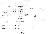
图1是表示第一实施方式的存储器控制装置190的功能结构一例的方框图。在图1中,同存储器控制装置190一起,表示了第1主板100、第2主板130、第3主板150、及外部存储器180。FIG. 1 is a block diagram showing an example of a functional configuration of a memory control device 190 according to the first embodiment. In FIG. 1 , together with the memory control device 190 , the
第1主板100、第2主板130、第3主板150分别经存储器控制装置190存取外部存储器180上的数据。The first
存储器控制装置190是处理从各主板对位于由各主板共有的外部存储器180的共有区域181中的数据的存取请求的装置,包括分别对应第1主板100、第2主板130、第3主板150而设置的第1主板I/F(接口)110、第2主板I/F140、第3主板I/F160、以及外部存储器I/F170。The memory control device 190 is a device for processing access requests from each main board to data in the
外部存储器180与外部存储器I/F170连接,包含共有区域181和特定区域182。The
共有区域181是外部存储器180上的一部分区域,保存在各主板间共有的数据。具体地,共有区域180例如用于从第2主板130向第1主板100的数据传递。The shared
特定区域182是存在于外部存储器180上,例如由于外部存储器I/F在改变存取定时的同步(recync)等的存取控制时使用,用禁止从各主板存取的特定地址表示的区域。The
第1主板100与第1主板I/F110连接,具有CPU101。The first
当重写共有区域181上的数据时,第2主板130对第1主板100输出中断请求信号。当输入了此信号时,第1主板100的CPU101通过向第1主板I/F110输出读访问请求,开始读取共有区域181上的已被重写的数据。When rewriting data on the
第1主板I/F110是接收来自第1主板100的存取请求、发行对外部存储器I/F170的存取请求的接口,包括缓冲器控制部111和特定存取检测部123。The first motherboard I/
缓冲器控制部111包括数据缓冲器112、地址缓冲器113、及第1比较部114。特定地址检测部123包括缓冲器无效化部120、第2比较部121、及特定地址寄存器122。The
数据缓冲器112保存外部存储器180上的至少一部分数据的复制。
地址缓冲器113保存被保存在数据缓冲器112的数据的地址。The
第1比较部114通过比较从第1主板100请求存取的地址、和保存在地址缓冲器113的地址,输出表示从第1主板100请求存取的地址在被保存在数据缓冲器112的数据的地址范围内是否一致的第1比较信息。The
当从缓冲器无效化部120未输出无效化控制信号、且第1比较部114的第1比较信息表示不一致时,缓冲器控制部111对外部存储器I/F170发行存取请求,当表示一致时,向第1主板100输出被保存在数据缓冲器112的数据。When the invalidation control signal is not output from the
从CPU101将外部存储器180中的特定区域182的地址设定并保存在特定地址寄存器122。The address of the
第2比较部121比较从第1主板100请求存取的地址、和被保存在特定地址寄存器122的地址,向缓冲器无效化部120输出表示是否一致的第2比较信息。The second comparison unit 121 compares the address requested for access from the
缓冲器无效化部120从第2比较部121取得第2比较信息,在取得的第2比较信息表示一致时,向缓冲器控制部111输出无效化控制信号。The
如果输入了该无效化控制信号,缓冲器控制部111对数据缓冲器112进行无效化,立即向第1主板100发出存取响应。由此,从第1主板100请求下一次存取时,与第1比较部114的第1比较信息无关,发行对外部存储器I/F170的存取请求。When the invalidation control signal is input, the
数据缓冲器112的无效化具体地是例如用无效的地址更新地址缓存器113进行的,以使第1比较部114同本来的比较结果无关地输出表示不一致的第1比较信息。而且,也可以是,设置表示数据缓冲器是否被无效化的未图示的寄存器,通过更新其内容进行。Specifically, the
第2主板130与第2主板I/F140连接。The second
第2主板I/F140接受来自第2主板130的存取请求,发行对外部存储器I/F170的存取请求。The second main board I/
第3主板150与第3主板I/F160连接。The third
第3主板I/F160接受来自第3主板150的存取请求,发行对外部存储器I/F170的存取请求。The third main board I/
第2主板I/F140及第3主板I/F160分别具有与第1主板I/F110相同的结构,所以省略说明。Since the second main board I/
外部存储器I/F170接受来自第1主板I/F110、第2主板I/F140、第3主板I/F160的各自的存取请求,对外部存储器180进行存取。External memory I/
下面,说明第一实施方式的动作例。Next, an operation example of the first embodiment will be described.
图2是表示第一实施方式的存储器控制装置190的动作例的流程图。FIG. 2 is a flowchart showing an operation example of the memory control device 190 according to the first embodiment.
第1主板100对特定地址寄存器122设定表示外部存储器180上的特定区域182的地址值(S1101)。The
当向外部存储器180上的共有区域181写入了对第1主板100进行传递的数据(S1102)时,第2主板130为了通知应传递的数据已准备好的信息,对第1主板100发行中断请求(S1103)。When the data to be transferred to the first
当第1主板100接受了来自第2主板130的中断请求时,对在通常动作时被禁止存取的外部存储器180上的特定区域182发行写访问请求(S1104)。为了处理该写访问请求,调用作为子程序的第一处理(S1107)。第一处理的详细内容在后面叙述。When the first
第1主板100为了读取由第2主板130写入到外部存储器180上的共有区域181的数据,发行读访问请求(S1105)。为了处理该读访问请求,调用第一处理(S1113)。The first
第1主板100在写入到共有区域181中的数据的读取结束之前,返回S1105发行读访问请求(S1106中的“否”),当读取结束时,结束动作(S1106中的“是”)。The first
下面,说明第一处理。该处理是由第1主板I/F110执行的子程序处理。Next, the first processing will be described. This processing is performed by a subroutine executed by the first main board I/
在来自第2比较部121的第2比较信息表示一致时(S1108的“是”),缓冲器无效化部120通过向缓冲器控制部111输出无效化控制信号,缓冲器控制部111对数据缓冲器112进行无效化,控制成立即对第1主板100进行存取响应(S1109)。在此要注意的是,该存取响应是在与从向外部存储器I/F170发行存取请求开始到进行存取响应的时间相比,充分短的时间内进行。When the second comparison information from the second comparison unit 121 indicates a match (Yes in S1108), the
在第2比较信息表示不一致时,不输出无效化控制信号(S1108的“否”),如果来自第1比较部114的第1比较信息表示一致(S1110的“是”),缓冲器控制部111向第1主板100输出被保存在数据缓冲器112的数据(S1111),如果第1比较信息表示不一致(S1110的“否”),缓冲器控制部111向外部存储器I/F170发行存取请求(S1112)。When the second comparison information indicates inconsistency, the invalidation control signal is not output ("No" in S1108), and if the first comparison information from the
而且,在初始状态下,数据缓冲器112也可以被无效化。如果这样,在最初调用的第一处理中,第1比较信息和第2比较信息都表示不一致(在S1108和S1110都是“否”),必须在步骤S1112发行对外部存储器I/F170的存取请求。Furthermore, in the initial state, the
根据以上结构,可以在数据缓冲器以外的外部存储器上设定用于数据缓冲器的无效化的特定地址。为此,在主板随机地存取数据缓冲器内的数据时,不会进行不希望的数据缓冲器的无效化,可以防止数据缓冲器的命中率的下降,可以有效地对外部存储器进行存取。According to the above configuration, a specific address for invalidating the data buffer can be set in an external memory other than the data buffer. For this reason, when the motherboard randomly accesses the data in the data buffer, the invalidation of the data buffer will not be undesired, the decrease in the hit rate of the data buffer can be prevented, and the external memory can be accessed efficiently. .
而且,在特定的主板对由其它主板重写的外部存储器上的数据进行轮询存取那样,根据需要进行用于无效化的存取时,也不进行对外部存储器的存取,所以,可以省略无用的存取。In addition, when a specific main board performs polling access to data on the external memory rewritten by other main boards, when access for invalidation is performed as needed, access to the external memory is not performed, so it is possible Useless accesses are omitted.
由此,不会因无效化增大对外部存储器的存取负载,而且,在无效化后必须立即进行对外部存储器的存取,所以,能够确实地得到数据缓冲器和外部存储器间的匹配性。Therefore, the access load to the external memory will not be increased due to invalidation, and the access to the external memory must be performed immediately after invalidation, so that the match between the data buffer and the external memory can be reliably obtained. .
在第一实施方式中,说明了将外部存储器上的特定区域的一部分地址作为用于数据缓冲器的无效化的特定地址而利用的结构。In the first embodiment, a configuration is described in which some addresses in a specific area on the external memory are used as specific addresses for invalidating the data buffer.
但是,在第一实施方式的结构中,当外部存储器I/F在存取控制时使用的特定区域不明确时、或者不能确保时,存在不能设定特定地址的课题。为了解决这样的课题,希望不使用外部存储器上的特定区域就可以进行数据缓冲器的无效化的结构。However, in the configuration of the first embodiment, if the specific area used by the external memory I/F for access control is unclear or cannot be secured, there is a problem that a specific address cannot be set. In order to solve such a problem, it is desirable to have a structure that can invalidate the data buffer without using a specific area on the external memory.
下面,在第二实施方式说明这样的结构。Next, such a structure will be described in the second embodiment.
(第二实施方式)(second embodiment)
图3是表示第二实施方式的存储器控制装置191的功能结构一例的方框图。在图3中,与存储器控制装置191一起,表示了第1主板100、第2主板130、第3主板150以及外部存储器180。FIG. 3 is a block diagram showing an example of the functional configuration of the
存储器控制装置191是将在第一实施方式中说明的存储器控制装置190(参照图1)的第1主板I/F110的特定存取检测部123替换为特定存取检测部224而构成。在图3中,对于与存取控制装置190相同的功能模块付与相同标记,省略其说明。The
特定存取检测部224是在发生了对同一地址的连续的存取请求时,将缓冲器控制部111控制成每隔一次强制地对外部存储器180进行存取的单元,包括缓冲器更新部220、缓冲器存取历史保存部221以及第3比较部223。The specific
当有来自第1主板100的存取请求时,缓冲器存取历史保存部221保存表示根据该存取请求进行的存取是对外部存储器I/F170的存取、还是对数据缓冲器112的存取的历史信息。When there is an access request from the
该历史信息具体地表示根据来自第1主板100的上述存取请求是发行了对外部存储器I/F170的存取请求、还是从数据缓冲器112向第1主板100进行了数据输出。The history information specifically indicates whether an access request to the external memory I/
第3比较部223比较从第1主板100请求存取的地址和被保存在地址缓冲器113的地址,向缓冲器更新部220输出是否完全一致的第3比较信息。The
缓冲器更新部220从第3比较部223取得第3比较信息,而且从缓冲器存取历史保存部221取得历史信息。然后,当第3比较信息表示一致、且历史信息表示对数据缓冲器的存取时,向缓冲器控制部111输出更新控制信号。如果提供了该更新控制信号,缓冲器控制部111同第1比较部114的第1比较信息无关地发行对外部存储器I/F170的存取请求。The
下面,说明第二实施方式的动作例。Next, an operation example of the second embodiment will be described.
图4是表示第二实施方式的存储器控制装置191的动作例的流程图。FIG. 4 is a flowchart showing an operation example of the
对于与动作的说明1中说明的存储器控制装置190的动作例(参照图2)相同的步骤,付与相同标记,省略其说明。The steps that are the same as those in the example of the operation of the memory control device 190 (see FIG. 2 ) described in Description of
当第1主板100接受到来自第2主板130的中断请求时,预备地发行对预定为从共有区域首先读取数据的地址的读访问请求(S1201)。为了处理该读访问请求,调用作为子程序的第二处理(S1202)。第二处理的详细内容在下面叙述。When the first
之后,第1主板100为了读取由第2主板130写入到外部存储器180上的共有区域181的数据,发行读访问请求。为了处理该读访问请求,调用第二处理(S1205)。Thereafter, the first
在第二处理中,在来自第3比较部223的第3比较信息表示一致时(S1203的“是”),如果缓冲器存取历史保存部221的历史信息表示对数据缓冲器112的存取(S1204的“是”),缓冲器更新部220通过向缓冲器控制部111输出第1更新控制信号,进行使缓冲器控制部111发行对外部存储器I/F170的存取请求的控制(S1112)。而且,若缓冲器存取历史保存部221的历史信息表示对外部存储器180的存取(S1204的“否”),缓冲器更新部220通过向缓冲器控制部111输出第2更新控制信号,进行使缓冲器控制部111向第1主板100(S1111)输出数据缓冲器112的控制。In the second process, when the third comparison information from the
另一方面,在来自第3比较部223的第3比较信息表示不一致时,不输出第1及第2更新控制信号(S1203的“否”),如果来自第1比较部114的第1比较信息表示一致(S1110的“是”),缓冲器控制部111向第1主板100输出被保存在数据缓冲器112的数据(S1111),若第1比较信息表示不一致(S1110的“否”,缓冲器控制部111向外部存储器I/F170发行存取请求(S1112)。On the other hand, when the third comparison information from the
在此,说明了利用步骤S1201中的预备的读访问,在步骤S1105的最初的数据读取中,不增加对外部存储器的存取负载,就可以保证数据缓冲器和外部存储器间的匹配性。Here, it is explained that by using the preliminary read access in step S1201, in the initial data reading in step S1105, the compatibility between the data buffer and the external memory can be ensured without increasing the access load to the external memory.
在步骤S1201,发行了对预定为从共有区域最初读取的数据的预备的读访问请求,所以,在通过步骤S1105的最初的数据读取调用的步骤S1203中,第3比较信息一定表示一致。In step S1201, a preliminary read access request is issued for the data to be first read from the common area, and therefore, in step S1203 through the first data read call in step S1105, the third comparison information always indicates a match.
在步骤S1204参照缓冲器存取历史保存部221的历史信息。此时的历史信息,根据上述的预备的读访问请求,表示是数据缓冲器112被存取、还是外部存储器180被存取。In step S1204, the history information of the buffer access
在示出了对数据缓冲器112的存取时,在步骤S1112发行对外部存储器I/F的读访问请求,取得最新的数据,所以保证了数据缓冲器112和外部存储器180间的匹配性。When an access to the
另一方面,在示出了对外部存储器180的存取时,在步骤S1111输出数据缓冲器的数据,但其内容是用刚才的预备的存取请求从外部存储器刚取得的最新内容,也保证了数据缓冲器112和外部存储器180间的匹配性。On the other hand, when the access to the
并且,在此两种情况的任意一个中,对外部存储器180的存取一次就可以。And, in either of these two cases, one access to the
根据以上的结构,通过将存取开始地址使用于假存取,即使在外部存储器180上不能设定第一实施方式中记述的那样的特定区域的情况下,也可以获得不增加对外部存储器的无用的存取时间就能够实现数据缓冲器的无效化的效果。According to the above configuration, by using the access start address for the dummy access, even when the specific area described in the first embodiment cannot be set on the
在第二实施方式中,说明了通过对连续的同一地址的读访问,不会增加对外部存储器的无用的存取就能够从外部存储器取得最新数据的结构。In the second embodiment, a configuration is described in which the latest data can be acquired from the external memory without increasing useless access to the external memory by consecutive read accesses to the same address.
但是,在第一实施方式和第二实施方式中存在如下课题,即,为了对数据缓冲器进行无效化从外部存储器取得最新数据,通过程序的执行,需要有意识地发行对特定地址的事先的读访问、或对存取开始地址的预备的读访问,换句话说,需要利用软件的管理。为了解决这样的课题,希望不利用软件的管理就可以进行数据缓冲器的无效化的结构。However, in the first and second embodiments, in order to invalidate the data buffer to obtain the latest data from the external memory, it is necessary to consciously issue a prior read to a specific address by executing the program. Access, or preparatory read access to the access start address, in other words, requires management by software. In order to solve such a problem, it is desirable to have a configuration that can invalidate the data buffer without software management.
下面,用第三实施方式和第四实施方式说明这样的结构。Hereinafter, such a configuration will be described using the third and fourth embodiments.
(第三实施方式)(third embodiment)
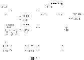
图5是表示第三实施方式的存储器控制装置192的功能结构一例的方框图。在图5中,同存储器控制装置192一起,表示了第1主板100、第2主板130、第3主板150以及外部存储器180。FIG. 5 is a block diagram showing an example of the functional configuration of the
存储器控制装置192是在第一实施方式中说明的存储器控制装置190(参照图1)上追加了假存取发行部302的结构。在图5中,对于与存储器控制装置190相同的功能模块,付与相同的标记,并省略其说明。The
假存取发行部302是从第2主板130接受表示外部存储器180上的共有区域181的数据被更新的通知即中断请求,向第1主板I/F110发行对如上所述的特定地址的存取请求的单元。The dummy
当假存取发行部302从第1主板I/F110接收到对上述存取请求的响应时,向CPU101发行存取结束通知。When receiving a response to the access request from the first motherboard I/
在此,也可以考虑为,中断请求和存取结束通知是相同规格的信号,假存取发行部302中继在第一实施方式中从第2主板130向CPU101供给的中断请求。Here, it is conceivable that the interrupt request and the access end notification are signals of the same specification, and that the dummy
(动作的说明3)(explanation 3 of movement)
下面,说明第三实施方式的动作例。Next, an operation example of the third embodiment will be described.
图6是表示第三实施方式的存储器控制装置192的动作例的流程图。FIG. 6 is a flowchart showing an operation example of the
对于与动作说明1中说明的存储器控制装置190的动作例(参照图2)相同的步骤,付与相同的标记,省略其说明。The same steps as those in the operation example (see FIG. 2 ) of the memory control device 190 described in
当假存取发行部302接受了中断请求时,向第1主板I/F110发行对特定地址的存取请求(在下面,还称为假存取请求)(S1301)。When receiving the interrupt request, the dummy
然后,当假存取发行部302从第1主板I/F110接受到存取响应时,向CPU101发行存取结束通知(S1302)。Then, when receiving an access response from the first motherboard I/
通过以上的结构,从假存取发行部302向第1主板I/F110发行用于无效化的存取,所以具有不需要使用软件有意识地发行假存取请求,并且能够保证数据缓冲器和外部存储器间的匹配性这一点不变化的效果。With the above configuration, since the dummy
(第四实施方式)(fourth embodiment)
下面说明第四实施方式的构成。Next, the configuration of the fourth embodiment will be described.
图7是表示第四实施方式的存储器控制装置193的功能结构一例的方框图。在图7中,同存储器控制装置193一起,表示了第1主板100、第2主板130、第3主板150以及外部存储器180。FIG. 7 is a block diagram showing an example of the functional configuration of the memory control device 193 according to the fourth embodiment. In FIG. 7 , the first
存储器控制装置193是在第二实施方式中说明的存储器控制装置191(参照图3)上追加了假存取发行部402的结构。在图7中,对于与存储器控制装置191相同的模块,付与相同的标记,省略其说明。The memory control device 193 is configured by adding the dummy access issuing unit 402 to the memory control device 191 (see FIG. 3 ) described in the second embodiment. In FIG. 7 , the same blocks as those of the
假存取发行部402是从第2主板130接受表示外部存储器180上的共有区域181的数据被更新的通知即中断请求,向第1主板I/F210发行对上述特定地址的存取请求的单元。The dummy access issuing unit 402 is a unit that receives an interrupt request from the second
当假存取发行部402从第1主板I/F110接收到对上述存取请求的响应时,向CPU101发行存取结束通知。When receiving a response to the access request from the first motherboard I/
在此,也可以考虑为,中断请求和存取结束通知是相同规格的信号,假存取发行部402中继在第二实施方式从第2主板130向CPU101供给的中断请求。Here, it is conceivable that the interrupt request and the access end notification are signals of the same standard, and that the dummy access issuing unit 402 relays the interrupt request supplied from the second
(动作的说明4)(explanation 4 of movement)
下面,说明第四实施方式的动作例。Next, an operation example of the fourth embodiment will be described.
图8是表示第四实施方式的存储器控制装置193的动作例的流程图。FIG. 8 is a flowchart showing an operation example of the memory control device 193 according to the fourth embodiment.
对于与动作说明2中说明的存储器控制装置191的动作例(参照图4)相同的步骤,付与相同的标记,省略其说明。The same steps as those in the operation example (see FIG. 4 ) of the
当假存取发行部302接受到中断请求时,向第1主板I/F210发行对从共有区域最初读取的数据的地址的假存取请求(S1401)。When receiving the interrupt request, the dummy
然后,当假存取发行部402从第1主板I/F210接收到存取响应时,向CPU101发行存取结束通知(S1402)。Then, when receiving an access response from the first motherboard I/
通过以上的结构,从假存取发行部402向第1主板I/F210发行用于无效化的存取,所以,具有不需要利用软件有意识地发行假存取,并且能够保证数据缓冲器和外部存储器间的匹配性这一点不改变的效果。With the above configuration, since the dummy access issuing unit 402 issues an access for invalidation to the first motherboard I/
并且,在第三实施方式和第四实施方式中,说明了如下结构,即代替第1主板100的CPU101,由假存取发行部302及402发行假存取请求,但也可以在具备DMAC(DMA控制器)的主板中适用假存取发行部。该情况下,上述的中断请求表示DMAC的启动请求。DMAC通常不具备用于发行假存取的程序执行功能,所以用DMAC代替假存取发行部发行假存取请求的意义很大。Furthermore, in the third embodiment and the fourth embodiment, the configuration is described in which the dummy access request is issued by the dummy
在第三实施方式及第四实施方式,说明了代替第1主板100的CPU101,由假存取发行部302及402发行假存取请求,由此不需要软件的管理并且能保证数据缓冲器和外部存储器间的匹配性的结构。此外,说明了这样的结构特别适用于具备DMAC的主板。In the third embodiment and the fourth embodiment, instead of the
但是,通常DMAC具有多个通道,其中,可以考虑到,例如像从外部输入输出器件传送数据的通道那样,如果在发生了启动请求时进行假存取,那么存在会产生最初数据被读丢的问题的通道。为此,希望是能够对每个通道或每个启动要因禁止假存取请求的发行的结构。However, a DMAC generally has a plurality of channels. Among them, it can be considered that, for example, as a channel for transferring data from an external I/O device, if a false access is performed when a start request occurs, there is a possibility that the initial data will be read and lost. channel of the problem. Therefore, it is desirable to have a structure that can prohibit issuance of false access requests for each channel or each activation factor.
下面,用第五实施方式和第六实施方式说明那样的结构。Next, such a configuration will be described using the fifth and sixth embodiments.
(第五实施方式)(fifth embodiment)
图9是表示第五实施方式的存储器控制装置194的功能结构一例的方框图。在图9中,同存储器控制装置194一起,表示了第1主板500、第2主板130、第3主板150以及外部存储器180。FIG. 9 is a block diagram showing an example of the functional configuration of the
存储器控制装置194具备在DMAC通道所固有的假存取发行部504及假存取控制寄存器503,来代替第四实施方式中说明的存储器控制装置193(参照图7)的假存取发行部402。在图9中,对于与存储器控制装置193相同的功能模块,付与相同的标记,省略其说明。而且,省略第1主板I/F210的详细记载。The
第1主板500包括CPU101及DMAC501。DMAC501是三通道的DMA控制器,包括第1通道502、第2通道505、及第3通道506。在第1通道502中表示的假存取发行部504及假存取控制寄存器503是存储器控制装置194的一部分。The
当第1通道502从第2主板130接受了启动请求时,根据在例如未图示的构成寄存器中预先设定的内容,开始数据传送。When the
假存取控制寄存器503保存在第1通道502接受了启动请求时是否发行假存取(是允许,还是禁止)的设定,并且向假存取发行部504输出设定内容。The dummy
同样的假存取控制寄存器,也分别设置在第2通道505、第3通道506(省略图示)。The same dummy access control registers are also provided in the
当假存取发行部504接受了启动请求时,如果在假存取控制寄存器503中被设定为允许,那么发行与上述假存取发行部402发行的假存取请求相同的假存取请求,如果被设定为禁止,那么禁止上述假存取请求的发行。When false
同样的假存取发行部,也分别设置在第2通道505、第3通道506(省略图示)。Similar dummy access issuing units are also provided in the
第2通道505、及第3通道506具有与第1通道502相同的结构,当分别接受了启动请求时,在根据假存取控制寄存器的设定内容发行了假存取请求之后,开始预定的数据的传送。The
(第五实施方式)(fifth embodiment)
下面,说明第五实施方式的动作例。Next, an operation example of the fifth embodiment will be described.
图10是表示第五实施方式的存储器控制装置194的动作例的流程图。FIG. 10 is a flowchart showing an operation example of the
对于与动作说明4中说明的存储器控制装置193的动作例(参照图8)相同的步骤,付与相同标记,省略其说明。在此,设假存取发行部504发行与假存取发行部402发行的假存取请求相同的假存取请求,进行说明。The same steps as those in the example of the operation of the memory control device 193 (see FIG. 8 ) described in Operation Description 4 are assigned the same symbols, and their descriptions are omitted. Here, a description will be given assuming that the dummy
CPU101对每个通道进行是否向假存取控制寄存器503发行假存取请求的设定(S1501)。The
当外部存储器180上的共有区域181被更新、从第2主板130接受了作为中断请求的对第1通道502的启动请求时,被请求启动的第1通道502的假存取发行部504参照假存取控制寄存器503的内容,如果设定为允许(S1502的“是”),向第1主板I/F210发行对从共有区域181最初读取的数据的地址的假存取请求,若设定为禁止,禁止上述假存取请求的发行(S1502的“否”)。When the
然后,DMAC501的第1通道502进行共有区域181的数据存取(S1105~S1106)。Then, the
根据以上的结构,可以对每个通道控制DMAC启动时的假存取发行的有无,所以,具有对于不需要假存取、或者假存取有害的通道可以禁止启动时的假存取发行的效果。According to the above structure, it is possible to control the presence or absence of false access issuance at the time of DMAC activation for each channel. Therefore, it is possible to prohibit the issuance of false access at the time of activation for channels that do not require false access or are harmful to false access. Effect.
(第六实施方式)(sixth embodiment)
下面,说明第六实施方式的结构。Next, the configuration of the sixth embodiment will be described.
图11是表示第六实施方式的存储器控制装置195的功能结构一例的方框图。在图11,与存储器控制装置195一起,表示了第1主板600、第2主板130、第3主板150以及外部存储器180。FIG. 11 is a block diagram showing an example of the functional configuration of the
存储器控制装置195具有DMAC的通道所固有的假存取发行部603、以及通道中共通的假存取控制寄存器606,来代替在第四实施方式中说明的存储器控制装置193(参照图7)的假存取发行部402。在图11中,对于与存储器控制装置193相同的功能模块,付与相同的标记,省略其说明。而且,省略第1主板I/F210的详细记载。The
第1主板600包括CPU101、DMAC601、SIF(串行接口)607、及TIMER(定时器)608。DMAC501是三通道的DMA控制器,包括第1通道602、第2通道604、以及第3通道605。而且,如图所示,根据分别与第2主板130、SIF607以及TIMER608的三种启动要因对应的第1启动请求、第2启动请求以及第3启动请求,进行启动。The first
在DMAC601及第1通道602中表示的假存取控制寄存器606及假存取发行部603是存储器控制装置195的一部分。The dummy
当第1通道602从第2主板130接受了启动请求时,按照在例如未图示的构成寄存器中预先设定的内容,开始数据传送。When the
假存取控制寄存器606由第1通道602、第2通道604、第3通道605共用,按每个启动要因、即第1至第3启动请求的每个,保存在接受了启动请求时是否发行假存取(是允许,还是禁止)的设定,向第1通道602至第3通道605输出设定内容。The dummy
当假存取发行部603接受了第1至第3启动请求的一个时,如果对于接受的启动请求在假存取控制寄存器606设定为允许,那么发行与上述假存取发行部402发行的假存取请求相同的假存取请求,如果设定为禁止,则禁止上述假存取请求的发行。When false
同样的假存取发行部也分别设在第2通道604、第3通道605(省略图示)。Similar dummy access issuing units are also provided in the
第2通道604及第3通道605具有与第1通道602相同的构成,当分别接受了第1至第3启动请求的一个时,根据假存取控制寄存器606的设定内容发行了假存取请求之后,开始预定的数据传送。The
(动作说明6)(Action description 6)
下面,说明第六实施方式的动作例。Next, an operation example of the sixth embodiment will be described.
图12是表示第六实施方式的存储器控制装置195的动作例的流程图。FIG. 12 is a flowchart showing an operation example of the
对于与动作说明4中说明的存储器控制装置193的动作例(参照图8)相同的步骤,付与相同标记,省略其说明。在此,设假存取发行部603发行与假存取发行部402发行的假存取请求相同的假存取请求,进行说明。The same steps as those in the example of the operation of the memory control device 193 (see FIG. 8 ) described in Operation Description 4 are assigned the same symbols, and their descriptions are omitted. Here, a description will be given assuming that the dummy
CPU101对每个启动要因进行是否向假存取控制寄存器606发行假存取请求的设定(S1601)。The
当外部存储器180上的共有区域181被更新、从第2主板130接受了作为中断请求的第1启动请求时,向与第1启动请求预先建立了对应的通道(在此设为第1通道602)通知上述第1启动请求。When the
当第1通道602接受了上述第1启动请求时,参照假存取控制寄存器606的内容,如果对第1启动请求设定为允许(S1602的“是”),则向第1主板I/F210发行对从共有区域181最初读取的数据的地址的假存取请求(S1602),如果设定为禁止,则禁止上述假存取请求的发行(S1602的“否”)。When the
然后,DMAC601的第1通道602进行共有区域181的数据的存取(S1105~S1106)。Then, the
根据以上的结构,能够按每个启动要因控制DMAC启动时的假存取发行的有无,所以,具有对于不需要假存取、或者假存取有害的启动要因能够禁止启动时的假存取发行的效果。According to the above configuration, it is possible to control the presence or absence of false access issuance at the time of DMAC activation for each activation factor, so that false access at the time of activation can be prohibited for activation factors that do not require false access or are harmful to false access. The effect of the release.
在背景技术部分,在主板间不进行排他控制的比较简单的系统中,特定的主板为了检测出位于外部存储器上的系统的状态被其它主板重写的情况,在对特定的地址进行轮询存取时,重复进行对相同地址的读取,所以,存在数据缓冲器被连续命中、不能取得与外部存储器的匹配性的课题,并指出了现有技术没有公开示其解决方法。In the background technology section, in a relatively simple system without exclusive control between motherboards, a specific motherboard polls a specific address in order to detect that the state of the system on the external memory is overwritten by other motherboards. When fetching, the same address is repeatedly read, so there is a problem that the data buffer is continuously hit and compatibility with the external memory cannot be obtained, and it is pointed out that the prior art does not disclose a solution to this problem.
为解决这样的课题,希望具有在例如进行轮询存取时能够确实地取得与外部存储器的匹配性的结构。In order to solve such a problem, it is desirable to have a configuration that can reliably acquire compatibility with the external memory when, for example, polling access is performed.
下面,在第七实施方式中说明其结构。Next, the structure of the seventh embodiment will be described.
(第七实施方式)(seventh embodiment)
图13是表示第七实施方式的存储器控制装置196的功能结构一例的方框图。在图13中,与存储器控制装置196一起,表示了第1主板100、第2主板130、第3主板150以及外部存储器180。FIG. 13 is a block diagram showing an example of the functional configuration of the
存储器控制装置196是将第一实施方式中说明的存储器控制装置190(参照图1)的第1主板I/F110中的特定存取检测部123替换为特定存取检测部723而构成。在图13中,对于与存储器控制装置190相同的功能模块,付与相同的标记,省略其说明。The
特定存取检测部723是在连续发生具有相同存取信息的存取请求时,控制缓冲器控制部111以便在其第二次以后的存取请求中一定对外部存储器180进行存取、并且对缓冲器进行无效化的单元,包括缓冲器无效化部720、第4比较部721以及存取历史缓冲器722。The specific
在此,存取信息是指,来自第1主板100的存取请求所具有的参数的一部分或全部,地址、传送大小、读/写的指定是其一例。Here, the access information refers to a part or all of the parameters included in the access request from the
存取历史缓冲器722保存从第1主板100最后接受的存取请求所具有的存取信息。The
第4比较部721比较从第1主板100新接受的存取请求所具有的存取信息、和被保存在存取历史缓冲器722的存取信息,向缓冲器无效化部720输出表示是否一致的第4比较信息。The fourth comparison unit 721 compares the access information included in the access request newly received from the first
第4比较部721对地址一定进行该存取信息的比较,进一步,还可以对传送大小、读/写的指定进行。The fourth comparing unit 721 compares the access information with respect to the address, and further, may perform the designation of the transfer size and read/write.
缓冲器无效化部720从第4比较部721参照第4比较信息,在表示一致时,向缓冲器控制部111输出无效化控制信号。The
当缓冲器控制部111被提供该无效化控制信号时,与第1比较部114的第1比较信息无关地对数据缓冲器112进行无效化,发行对外部存储器I/F170的存取请求。此时,对外部存储器I/F170发行存取请求时的传送大小,使用由保存在存取历史缓冲器722的存取信息表示的传送大小,而且,读取的数据不保存在数据缓冲器112,而是输出到第1主板100。When the invalidation control signal is supplied to the
(动作说明7)(Action Description 7)
下面,说明第七实施方式的动作例。Next, an operation example of the seventh embodiment will be described.
图14是表示第七实施方式的存储器控制装置196的动作例的流程图。FIG. 14 is a flowchart showing an operation example of the
对于与动作说明1中说明的存储器控制装置190的动作例(参照图2)相同的步骤,付与相同标记,省略其说明。The same steps as those in the example of the operation of the memory control device 190 (see FIG. 2 ) described in
第1主板100为了检测出位于外部存储器180上的轮询地址的数据被重写为规定的期待值的情况,发行读访问请求(S1701)。为了处理该读访问请求,调用作为子程序的第三处理(S1703)。第三处理的详细内容后述。The first
第1主板100比较取得的数据和上述期待值,若不一致则返回到步骤S1701,继续进行定时查询(S1702的“否”),如果一致,则跳过定时查询循环(S1702的“是”),前进到规定的处理。The data that the
下面,说明第三处理。该处理是由第1主板I/F710执行的子程序处理。Next, the third processing will be described. This processing is performed by a subroutine executed by the first main board I/
缓冲器无效化部720参照第4比较部721的第4比较信息,在表示一致时(S1704的“是”),向缓冲器控制部111输出无效化控制信号。The
当缓冲器控制部111接受了该无效化控制信号时,与第1比较部114的第1比较信息无关地对数据缓冲器112进行无效化,并且向外部存储器I/F170发行请求从存取历史缓冲器722参照的传送大小的数据的存取请求。缓冲器控制部111不在数据缓冲器112中保存通过该存取请求从外部存储器180取得的数据,就向第1主板100输出(S1705)。When the
在第4比较信息表示不一致时,不输出无效化控制信号(S1704的“否”),根据第1比较信息进行对数据缓冲器或外部存储器的存取(S1110~S1112)。When the fourth comparison information indicates inconsistency, the invalidation control signal is not output ("No" in S1704), and the data buffer or external memory is accessed based on the first comparison information (S1110 to S1112).
通过以上的结构,当重复发行了相同的存取请求时,不是从数据缓冲器、而是从外部存储器进行读取,所以,在特定的主板向外部存储器上的特定地址进行轮询存取时,可以不需要软件的管理就可以保证数据缓冲器和外部存储器间的匹配性。而且,从外部存储器进行读取时,只对必要的传送大小分的数据进行存取请求,所以,具有可以减轻对外部存储器的存取负载的效果。With the above configuration, when the same access request is repeatedly issued, it is not from the data buffer but from the external memory, so when a specific motherboard performs polling access to a specific address on the external memory , the matching between the data buffer and the external memory can be guaranteed without software management. Furthermore, when reading from the external memory, only the necessary transfer size data is requested for access, so there is an effect that the load of access to the external memory can be reduced.
但是,根据第七实施方式的结构,如果重复发行相同的存取请求,那么数据缓冲器一定被无效化,所以,存在将来主板对外部存储器进行存取时的数据缓冲器的命中率下降,对外部存储器的存取效率恶化的课题。However, according to the structure of the seventh embodiment, if the same access request is repeatedly issued, the data buffer will be invalidated, so the hit rate of the data buffer will decrease when the main board accesses the external memory in the future. The problem of poor access efficiency of external memory.
下面,在第八实施方式说明解决其问题的结构。Next, in the eighth embodiment, a configuration for solving the problem will be described.
(第八实施方式)(eighth embodiment)
图15是表示第八实施方式的存储器控制装置197的功能结构一例的方框图。在图15,与存储器控制装置197一起,表示了第1主板100、第2主板130、第3主板150以及外部存储器180。FIG. 15 is a block diagram showing an example of the functional configuration of the
存储器控制装置197是将第七实施方式中说明的存储器控制装置196(参照图13)的第1主板I/F710中的特定存取检测部723替换为特定存取检测部821的结构。在图15中,对于与存储器控制装置196相同的功能模块,付与相同的标记,省略其说明。The
特定存取检测部821是在连续发生具有相同存取信息的存取请求时,控制缓冲器控制部111以便在其第二次以后的存取请求中一定进行对外部存储器180的存取、并且用从外部存储器180读取的数据更新数据缓冲器112的内容的单元,将上述的特定存取检测部723的缓冲器无效化部720替换为缓冲器更新部820构成。The specific
缓冲器更新部820从第4比较部721参照第4比较信息,在表示一致时,向缓冲器控制部111输出更新控制信号。The
当缓冲器控制部111被提供该更新控制信号时,与第1比较部114的第1比较信息无关地发行对外部存储器I/F170的存取请求。然后,向第1主板100输出读取的数据,并且用该数据更新数据缓冲器112的内容。When the update control signal is supplied to the
(动作的说明8)(explanation 8 of movement)
下面,说明第八实施方式的动作例。Next, an operation example of the eighth embodiment will be described.
图16是表示第八实施方式的存储器控制装置197的动作例的流程图。FIG. 16 is a flowchart showing an operation example of the
对于与动作说明7中说明的存储器控制装置196的动作例(参照图14)相同的步骤,付与相同标记,省略其说明。The same steps as those in the operation example of the
第1主板100执行发行对轮询地址的读访问请求的循环处理(S1701~S1702),由于处理该读访问请求,调用作为子程序的第四处理(S1801)。The first
在第四处理中,缓冲器更新部820参照第4比较部721的第4比较信息,在表示一致时(S1802的“是”),向缓冲器控制部111输出更新控制信号。In the fourth process, the
当缓冲器控制部111接受了该更新控制信号时,与第1比较部114的第1比较信息无关地向外部存储器I/F170发行存取请求(S1112)。缓冲器控制部111将通过该存取请求从外部存储器180取得的数据保存在数据缓冲器112,并且向第1主板100输出。When the
在第4比较信息表示不一致时,不输出更新控制信号(S1802的“否”),根据第1比较信息进行对数据缓冲器或外部存储器的存取(S1110~S1112)。When the fourth comparison information indicates inconsistency, the update control signal is not output ("No" in S1802), and the data buffer or external memory is accessed based on the first comparison information (S1110 to S1112).
通过以上的结构,在重复发行了相同存取请求时,数据缓冲器的内容也被更新,所以,将来具有能够防止主板对外部存储器进行存取时的数据缓冲的命中率下降的效果。With the above configuration, when the same access request is repeatedly issued, the contents of the data buffer are updated, so that it is possible to prevent the decrease in the hit rate of the data buffer when the main board accesses the external memory in the future.
但是,根据第七实施方式及第八实施方式的结构,在进行轮询存取期间,每次发生对外部存储器的存取请求,所以,具有来自CPU的存取延迟时间(latency,从CPU发出存取请求到实际取得数据为止的等待时间)变大、并且对外部存储器I/F的存取负载也不必要地增大的课题。However, according to the configurations of the seventh and eighth embodiments, an access request to the external memory is generated every time during the polling access period, so there is an access delay time (latency, issued from the CPU) from the CPU. The waiting time between the access request and the actual acquisition of data) increases, and the access load to the external memory I/F also increases unnecessarily.
下面,在第九实施方式说明解决该课题的结构。Next, a configuration for solving this problem will be described in the ninth embodiment.
(第九实施方式)(ninth embodiment)
图17是表示第九实施方式的存储器控制装置198的功能结构一例的方框图。在图17,与存储器控制装置198一起,表示了第1主板100、第2主板130、第3主板150以及外部存储器180。FIG. 17 is a block diagram showing an example of the functional configuration of the memory control device 198 according to the ninth embodiment. FIG. 17 shows the first
存储器控制装置196是将第八实施方式中说明的存储器控制装置197(参照图15)的第1主板I/F810及外部存储器I/F170分别替换为第1主板I/F910及外部存储器I/F970而构成。在图17中,对于与存储器控制装置197相同的功能模块,付与相同的标记,省略其说明。In the
第1主板I/F910具有在从外部存储器I/F970来的响应比对外部存储器180进行存取时更快时,向第1主板100输出数据缓冲器112的内容的功能。第1主板I/F910是在第1主板I/F810上追加特定存取部922和循环计数器921而构成。特定存取部922是将第1主板I/F810的特定存取检测部821中的缓冲器更新部替换为缓冲器选择部920而得到。The first main board I/F 910 has a function of outputting the contents of the
外部存储器I/F970是同外部存储器I/F170相比追加了管理轮询地址中的数据更新的有无,并且在无更新时对于来自第1主板I/F910的轮询地址的存取请求不对外部存储器180进行存取而尽早响应的功能的单元,是在外部存储器I/F170上追加了轮询地址设定寄存器971、轮询存取历史保存部972、及外部存储器选择部973而构成。Compared with the external memory I/F170, the external memory I/F970 is added to manage the presence or absence of data update in the polling address, and when there is no update, the access request to the polling address from the first motherboard I/F910 is incorrect. The
第1主板I/F910的各部分的详细功能如下。The detailed functions of each part of the first motherboard I/F910 are as follows.
缓冲器选择部920包含与缓冲器更新部820相同的功能,当从第1主板100有存取请求时,从第4比较部721参照第4比较信息,在表示一致时,向缓冲器控制部111输出更新控制信号。The buffer selection part 920 includes the same function as the
当缓冲器控制部111被提供该更新控制信号时,与第1比较部114的第1比较信息无关地发行对外部存储器I/F170的存取请求。When the update control signal is supplied to the
循环计数器921计测从缓冲器控制部111向外部存储器I/F970发行存取请求开始,直到返回存取响应信号的循环次数,向缓冲器选择部920通知计测的循环次数。The loop counter 921 counts the number of loops from when the
如果被通知的循环次数在规定循环以下,缓冲器选择部920向缓冲器控制部111输出第1选择控制信号,如果上述循环次数大于上述规定的循环,向缓冲器控制部111输出第2选择控制信号。If the notified number of cycles is less than a predetermined cycle, the buffer selection unit 920 outputs a first selection control signal to the
当缓冲器控制部111被提供了该第1选择控制信号时,向第1主板100输出数据缓冲器112的数据,当被提供了第2选择控制信号时,向第1主板100输出从外部存储器I/F970送回的数据,并且保存在数据缓冲器112。When the
而且,外部存储器I/F970的各部分的详细功能如下。Also, the detailed functions of each part of the external memory I/F 970 are as follows.
从各主板对轮询地址设定寄存器971任意地设定并保存用于轮询存取的外部存储器180上的轮询地址。The polling address on the
轮询存取历史保存部972保存表示数据缓冲器112和外部存储器180间是否有匹配性的状态值。作为具体的一例,该状态值也可以是,当接收了对从第1主板I/F910、第2主板I/F140、及第3主板I/F160的任一个设定在轮询地址设定寄存器971中的轮询地址的写访问请求时,就复位为“0”;当从第1主板I/F910接受了对上述轮询地址的读访问请求时,就设置为“1”;当从第1主板I/F910接受了对上述轮询地址以外的读访问请求时,就复位为“0”。The polling access history storage unit 972 stores a status value indicating whether or not there is a match between the
在此,状态值“1”表示外部存储器180的轮询地址中的当前数据也被取入到数据缓冲器112而考虑为有匹配性的状态,状态值“0”表示外部存储器180的数据被重写、或者在数据缓冲器112中取入轮询地址以外的数据而考虑为不具有匹配性的状态。Here, the status value "1" indicates that the current data in the polling address of the
当发生了从第1主板I/F910对上述轮询地址的读访问请求时,如果轮询存取历史保存部972的内容是状态值“0”,则外部存储器选择部973对外部存储器180进行存取,将取得的数据返回给第1主板I/F910;如果是状态值“1”,则外部存储器选择部973不对外部存储器180进行存取,而是立刻、即比对外部存储器180进行存取时更短时间内向第1主板I/F910返回响应信号。When a read access request to the polling address from the first motherboard I/F 910 occurs, if the content of the polling access history storage unit 972 is a state value “0”, the external memory selection unit 973 performs a process on the
(动作的说明9)(explanation 9 of the movement)
下面,说明第九实施方式的动作例。Next, an operation example of the ninth embodiment will be described.
图18是表示第九实施方式的存储器控制装置198的动作例的流程图。FIG. 18 is a flowchart showing an operation example of the memory control device 198 according to the ninth embodiment.
对于与动作说明8中说明的存储器控制装置197的动作例(参照图16)相同的步骤,付与相同标记,省略其说明。The same steps as those in the operation example of the
第1主板100执行发行对轮询地址的读访问请求的循环处理(S1701~S1702),为了处理该读访问请求,调用作为子程序的第5处理(S1901)。The first
在第5处理中,缓冲器选择部920参照第4比较部721的第4比较信息,当表示一致时(S1902的“是”),向缓冲器控制部111输出更新控制信号。In the fifth process, the buffer selection unit 920 refers to the fourth comparison information of the fourth comparison unit 721 , and when it indicates a match (YES in S1902 ), outputs an update control signal to the
当缓冲器控制部111接受了该更新控制信号时,与第1比较部114的第1比较信息无关地向外部存储器I/F970发行存取请求(S1903)。当发行了该存取请求时,循环计数器921开始循环次数的计测。When the
当外部存储器I/F970接受了该存取请求时,如上所述地,根据保存在轮询存取历史保存部972中的状态值,或者立刻返回存取响应信号、或者对外部存储器180进行存取而取得轮询地址中的最新数据,向第1主板I/F910返回该数据和存取响应信号。When the external memory I/F 970 accepts the access request, as described above, according to the state value stored in the polling access history storage unit 972, an access response signal is returned immediately, or the
当从外部存储器I/F970返回了存取响应信号时,循环计数器921向缓冲器选择部920通知至今计测的循环次数。When an access response signal is returned from the external memory I/F 970 , the loop counter 921 notifies the buffer selection unit 920 of the number of loops measured so far.
若通知的循环次数在规定的循环以下(S1904的“是”),缓冲器选择部920向缓冲器控制部111输出第1选择控制信号,缓冲器控制部111接受了该第1选择控制信号后,向第1主板100输出数据缓冲器112的数据(S1111)。If the number of cycles notified is less than the specified cycle ("Yes" in S1904), the buffer selection unit 920 outputs the first selection control signal to the
而且,若通知的循环次数大于上述规定的循环(S1904的“否”),缓冲器选择部920向缓冲器控制部111输出第2选择控制信号,缓冲器控制部111接受该第2选择控制信号后,向第1主板100输出从外部存储器I/F170返回的数据,并且保存在数据缓冲器112(S1905)。And, if the number of cycles notified is greater than the predetermined cycle ("No" in S1904), the buffer selection unit 920 outputs a second selection control signal to the
而且,当第4比较信息表示不一致时,不输出上述的更新控制信号(S1902的“否”),根据第1比较信息进行对数据缓冲器或外部存储器的存取(S1110~S1112)。And when the fourth comparison information indicates inconsistency, the above-mentioned update control signal is not output ("No" in S1902), and the data buffer or external memory is accessed based on the first comparison information (S1110-S1112).
通过以上结构,可以得到如下效果:即使在进行轮询存取期间,也不会每次发生对外部存储器的存取请求,抑制来自CPU的存取延迟时间,并且可以减轻对外部存储器I/F的存取负载。With the above structure, the following effects can be obtained: even during polling access, an access request to the external memory does not occur every time, the access delay time from the CPU can be suppressed, and the external memory I/F can be reduced. access load.
而且,通过在外部存储器I/F内具有轮询地址设定寄存器和轮询存取历史保存部、及外部存储器选择部,在外部存储器I/F以快的循环响应时,数据缓冲器的数据总能够再利用,并且发挥降低来自CPU的存取延迟时间的效果。Furthermore, by having a polling address setting register, a polling access history storage unit, and an external memory selection unit in the external memory I/F, when the external memory I/F responds in a fast cycle, the data in the data buffer It can always be reused and exhibits the effect of reducing the access delay time from the CPU.
涉及本发明的存储器控制装置是,在多个主板共有外部存储器、在主板间进行数据传递的系统中,具有保证在对应各主板的主板接口内具有的数据缓冲器和外部存储器间的数据匹配性的结构,所以,作为安装在DVD记录器的系统LSI等是有用的。Related to the memory control device of the present invention, in a system in which a plurality of mainboards share external memory and data is transferred between mainboards, the data compatibility between the data buffer and the external memory in the mainboard interface corresponding to each mainboard is guaranteed. Therefore, it is useful as a system LSI installed in a DVD recorder, etc.
Claims (17)
Translated fromChineseApplications Claiming Priority (2)
| Application Number | Priority Date | Filing Date | Title |
|---|---|---|---|
| JP271033/2005 | 2005-09-16 | ||
| JP2005271033AJP4834362B2 (en) | 2005-09-16 | 2005-09-16 | Memory controller. |
Publications (1)
| Publication Number | Publication Date |
|---|---|
| CN1932783Atrue CN1932783A (en) | 2007-03-21 |
Family
ID=37878627
Family Applications (1)
| Application Number | Title | Priority Date | Filing Date |
|---|---|---|---|
| CNA2006101534891APendingCN1932783A (en) | 2005-09-16 | 2006-09-15 | Memory control apparatus |
Country Status (3)
| Country | Link |
|---|---|
| US (1) | US7516254B2 (en) |
| JP (1) | JP4834362B2 (en) |
| CN (1) | CN1932783A (en) |
Cited By (3)
| Publication number | Priority date | Publication date | Assignee | Title |
|---|---|---|---|---|
| CN102473149A (en)* | 2009-07-20 | 2012-05-23 | 飞思卡尔半导体公司 | Signal processing system, integrated circuit comprising buffer control logic and method therefor |
| CN106371972A (en)* | 2016-08-31 | 2017-02-01 | 天津国芯科技有限公司 | Bus monitoring method and device for ensuring data consistency among primary equipment |
| CN106874230A (en)* | 2015-12-11 | 2017-06-20 | 南车株洲电力机车研究所有限公司 | The daughter board for being applied to PC/104 EBIs and the method for being applied to the daughter board |
Families Citing this family (7)
| Publication number | Priority date | Publication date | Assignee | Title |
|---|---|---|---|---|
| WO2007063858A1 (en)* | 2005-12-02 | 2007-06-07 | Matsushita Electric Industrial Co., Ltd. | Buffer control device and buffer memory |
| RU2419845C2 (en) | 2006-03-28 | 2011-05-27 | Панасоник Электрик Воркс Ко., Лтд. | Network system |
| JP2008139908A (en)* | 2006-11-29 | 2008-06-19 | Matsushita Electric Ind Co Ltd | MEMORY CONTROL DEVICE, COMPUTER SYSTEM, AND DATA REPRODUCTION / RECORDING DEVICE |
| EP2071468A4 (en) | 2006-12-25 | 2010-11-03 | Panasonic Corp | MEMORY CONTROL DEVICE, MEMORY DEVICE, AND MEMORY CONTROL METHOD |
| JP5130754B2 (en)* | 2007-03-15 | 2013-01-30 | 富士通セミコンダクター株式会社 | Semiconductor integrated circuit and memory system |
| KR101505005B1 (en)* | 2008-12-05 | 2015-03-24 | 삼성전자주식회사 | Memory device and management method of memory device |
| KR101056131B1 (en)* | 2009-07-09 | 2011-08-10 | 주식회사 디지털존 | Random Access Device and Random Access Method of Memory |
Family Cites Families (8)
| Publication number | Priority date | Publication date | Assignee | Title |
|---|---|---|---|---|
| JPS54148329A (en)* | 1978-05-15 | 1979-11-20 | Toshiba Corp | Buffer memory control system and information processor containing buffer memory |
| JPS62230164A (en)* | 1985-12-23 | 1987-10-08 | Nec Corp | Degital signal coding/decoding circuit |
| JP2936036B2 (en)* | 1992-10-27 | 1999-08-23 | 富士通株式会社 | Memory access device |
| JPH06243037A (en)* | 1993-02-18 | 1994-09-02 | Mitsubishi Electric Corp | Data look-ahead device |
| JPH06348593A (en)* | 1993-06-03 | 1994-12-22 | Sumitomo Electric Ind Ltd | Data transfer controller |
| US5953538A (en)* | 1996-11-12 | 1999-09-14 | Digital Equipment Corporation | Method and apparatus providing DMA transfers between devices coupled to different host bus bridges |
| JP4370063B2 (en) | 2001-06-27 | 2009-11-25 | 富士通マイクロエレクトロニクス株式会社 | Semiconductor memory device control device and semiconductor memory device control method |
| JP2003281084A (en) | 2002-03-19 | 2003-10-03 | Fujitsu Ltd | Microprocessor for efficient access to external bus |
- 2005
- 2005-09-16JPJP2005271033Apatent/JP4834362B2/ennot_activeExpired - Fee Related
- 2006
- 2006-09-07USUS11/470,742patent/US7516254B2/ennot_activeExpired - Fee Related
- 2006-09-15CNCNA2006101534891Apatent/CN1932783A/enactivePending
Cited By (6)
| Publication number | Priority date | Publication date | Assignee | Title |
|---|---|---|---|---|
| CN102473149A (en)* | 2009-07-20 | 2012-05-23 | 飞思卡尔半导体公司 | Signal processing system, integrated circuit comprising buffer control logic and method therefor |
| CN102473149B (en)* | 2009-07-20 | 2015-02-04 | 飞思卡尔半导体公司 | Signal processing system including buffer control logic, integrated circuit and method thereof |
| CN106874230A (en)* | 2015-12-11 | 2017-06-20 | 南车株洲电力机车研究所有限公司 | The daughter board for being applied to PC/104 EBIs and the method for being applied to the daughter board |
| CN106874230B (en)* | 2015-12-11 | 2020-01-03 | 南车株洲电力机车研究所有限公司 | Daughter board applied to PC/104 bus interface and method applied to daughter board |
| CN106371972A (en)* | 2016-08-31 | 2017-02-01 | 天津国芯科技有限公司 | Bus monitoring method and device for ensuring data consistency among primary equipment |
| CN106371972B (en)* | 2016-08-31 | 2019-04-05 | 天津国芯科技有限公司 | For solving the method for monitoring bus and device of data consistency between main equipment |
Also Published As
| Publication number | Publication date |
|---|---|
| US7516254B2 (en) | 2009-04-07 |
| JP4834362B2 (en) | 2011-12-14 |
| JP2007080220A (en) | 2007-03-29 |
| US20070088855A1 (en) | 2007-04-19 |
Similar Documents
| Publication | Publication Date | Title |
|---|---|---|
| CN1932783A (en) | Memory control apparatus | |
| CN101034381A (en) | Multi-master system and data transfer system | |
| CN1175341C (en) | Interface system and method for asynchronously updating shared resources | |
| CN1517869A (en) | Processor, arithmetic processing method, and priority determination method | |
| CN1280714C (en) | Multi-threaded processor that processes multiple instruction streams independently and softly controls the processing functions of each instruction stream | |
| CN1287282C (en) | Method and system for scheduling real-time periodic tasks | |
| CN1916961A (en) | Interruptible graphic processing unit and control method thereof | |
| CN1175034A (en) | Memory controller and memory control system | |
| CN1629815A (en) | Data processing system with multiple storage systems | |
| CN1912926A (en) | Method and graphics processing unit capable of interrupting graphics processing unit to process multiple programs | |
| CN1586063A (en) | Stream data processing device, stream data processing method, program, and medium | |
| CN1795434A (en) | Program execution control device, program execution control method, control program, and recording medium | |
| CN1916962A (en) | Method and device for storing and restoring state context in graphics processing unit | |
| CN1503150A (en) | Task allocation method in multiprocessor system and multiprocessor system | |
| CN1873689A (en) | Image processing device, method, and storage medium which stores a program | |
| CN1532666A (en) | Information processing device, clock pulse control method and control program of the device | |
| CN1947107A (en) | Device for transmitting data between memories | |
| CN1488097A (en) | Safe method for real-time operation of multitasking applications with error protection to determine control and command | |
| CN1873690A (en) | Image processing device, method, and storage medium which stores a program | |
| CN1315062C (en) | Processor apparatus, information processor using the same, compiling apparatus and method thereof | |
| CN1551592A (en) | Data transmission control device, electronic device and data transmission control method | |
| CN1890624A (en) | Electronic device and control method thereof, host device and control method thereof | |
| CN1385794A (en) | Data transmission controller, electronic device and data transmission method | |
| CN1383066A (en) | Memory controller and large scale integrated circuit | |
| CN1934543A (en) | Cache memory and control method thereof |
Legal Events
| Date | Code | Title | Description |
|---|---|---|---|
| C06 | Publication | ||
| PB01 | Publication | ||
| C10 | Entry into substantive examination | ||
| SE01 | Entry into force of request for substantive examination | ||
| AD01 | Patent right deemed abandoned | Effective date of abandoning:20070321 | |
| C20 | Patent right or utility model deemed to be abandoned or is abandoned |