CN1931522A - Dresser for dressing wafer polishing pad and manufacturing method thereof - Google Patents
Dresser for dressing wafer polishing pad and manufacturing method thereofDownload PDFInfo
- Publication number
- CN1931522A CN1931522ACNA2005101028310ACN200510102831ACN1931522ACN 1931522 ACN1931522 ACN 1931522ACN A2005101028310 ACNA2005101028310 ACN A2005101028310ACN 200510102831 ACN200510102831 ACN 200510102831ACN 1931522 ACN1931522 ACN 1931522A
- Authority
- CN
- China
- Prior art keywords
- trimmer
- grooves
- substrate
- manufacture method
- wafer grinding
- Prior art date
- Legal status (The legal status is an assumption and is not a legal conclusion. Google has not performed a legal analysis and makes no representation as to the accuracy of the status listed.)
- Pending
Links
- 238000004519manufacturing processMethods0.000titleclaimsabstractdescription26
- 238000005498polishingMethods0.000titleabstractdescription23
- 239000000758substrateSubstances0.000claimsabstractdescription30
- 239000000463materialSubstances0.000claimsabstractdescription27
- 238000000034methodMethods0.000claimsabstractdescription25
- 239000002245particleSubstances0.000claimsabstractdescription18
- 238000000227grindingMethods0.000claimsdescription19
- 230000001050lubricating effectEffects0.000claimsdescription13
- 238000009966trimmingMethods0.000claimsdescription12
- OKTJSMMVPCPJKN-UHFFFAOYSA-NCarbonChemical compound[C]OKTJSMMVPCPJKN-UHFFFAOYSA-N0.000claimsdescription11
- 229910052799carbonInorganic materials0.000claimsdescription11
- 229920000052poly(p-xylylene)Polymers0.000claimsdescription8
- UONOETXJSWQNOL-UHFFFAOYSA-Ntungsten carbideChemical compound[W+]#[C-]UONOETXJSWQNOL-UHFFFAOYSA-N0.000claimsdescription6
- 229910000679solderInorganic materials0.000claimsdescription4
- 238000005530etchingMethods0.000claims1
- 239000006061abrasive grainSubstances0.000description36
- 235000012431wafersNutrition0.000description16
- 238000005219brazingMethods0.000description8
- 229910045601alloyInorganic materials0.000description6
- 239000000956alloySubstances0.000description6
- 229910003460diamondInorganic materials0.000description6
- 239000010432diamondSubstances0.000description6
- 238000009713electroplatingMethods0.000description5
- 239000007788liquidSubstances0.000description5
- 229920002120photoresistant polymerPolymers0.000description4
- 239000003929acidic solutionSubstances0.000description3
- 239000012670alkaline solutionSubstances0.000description3
- 230000007547defectEffects0.000description3
- 239000000126substanceSubstances0.000description3
- XUIMIQQOPSSXEZ-UHFFFAOYSA-NSiliconChemical compound[Si]XUIMIQQOPSSXEZ-UHFFFAOYSA-N0.000description2
- 239000002253acidSubstances0.000description2
- 230000002378acidificating effectEffects0.000description2
- 239000003513alkaliSubstances0.000description2
- 229910052810boron oxideInorganic materials0.000description2
- 239000013078crystalSubstances0.000description2
- JKWMSGQKBLHBQQ-UHFFFAOYSA-Ndiboron trioxideChemical compoundO=BOB=OJKWMSGQKBLHBQQ-UHFFFAOYSA-N0.000description2
- 238000009826distributionMethods0.000description2
- 239000002184metalSubstances0.000description2
- 229910052751metalInorganic materials0.000description2
- 239000004065semiconductorSubstances0.000description2
- 229910052710siliconInorganic materials0.000description2
- 239000010703siliconSubstances0.000description2
- 238000001039wet etchingMethods0.000description2
- RYGMFSIKBFXOCR-UHFFFAOYSA-NCopperChemical compound[Cu]RYGMFSIKBFXOCR-UHFFFAOYSA-N0.000description1
- 239000000919ceramicSubstances0.000description1
- 229910052802copperInorganic materials0.000description1
- 239000010949copperSubstances0.000description1
- 238000005553drillingMethods0.000description1
- 230000000694effectsEffects0.000description1
- 238000005323electroformingMethods0.000description1
- 238000005516engineering processMethods0.000description1
- 239000000314lubricantSubstances0.000description1
- 238000012423maintenanceMethods0.000description1
- 239000007769metal materialSubstances0.000description1
- 150000002739metalsChemical class0.000description1
- 238000012986modificationMethods0.000description1
- 230000004048modificationEffects0.000description1
- 238000007517polishing processMethods0.000description1
- 229920002635polyurethanePolymers0.000description1
- 239000004814polyurethaneSubstances0.000description1
- 229920005749polyurethane resinPolymers0.000description1
- 239000011148porous materialSubstances0.000description1
- 239000010935stainless steelSubstances0.000description1
- 229910001220stainless steelInorganic materials0.000description1
- WFKWXMTUELFFGS-UHFFFAOYSA-NtungstenChemical compound[W]WFKWXMTUELFFGS-UHFFFAOYSA-N0.000description1
- 229910052721tungstenInorganic materials0.000description1
- 239000010937tungstenSubstances0.000description1
- 238000009827uniform distributionMethods0.000description1
- 239000012808vapor phaseSubstances0.000description1
- XLYOFNOQVPJJNP-UHFFFAOYSA-NwaterSubstancesOXLYOFNOQVPJJNP-UHFFFAOYSA-N0.000description1
Images


Landscapes
- Mechanical Treatment Of Semiconductor (AREA)
- Finish Polishing, Edge Sharpening, And Grinding By Specific Grinding Devices (AREA)
Abstract
Description
Translated fromChinese技术领域technical field
本发明涉及一种修整晶圆研磨垫的修整器及其制造方法,尤其涉及一种修整晶圆研磨垫的修整器及其制造方法,其中磨粒均匀地分布在修整器上,并稳固地固着在基板上。The invention relates to a dresser for dressing a wafer polishing pad and a manufacturing method thereof, in particular to a dresser for dressing a wafer polishing pad and a manufacturing method thereof, wherein abrasive grains are evenly distributed on the dresser and firmly fixed on the substrate.
背景技术Background technique
在目前半导体制造程序中,随着制造工艺的进步,芯片的线宽与面积都愈来愈小,而导线则愈来愈密集且需要堆栈愈来愈多层,此时芯片表面的平坦化也就越发重要,而化学机械研磨法(Chemical Mechanical Polishing,CMP)是目前唯一能提供全面性平坦化的一种技术。In the current semiconductor manufacturing process, with the progress of the manufacturing process, the line width and area of the chip are getting smaller and smaller, while the wires are getting denser and need to be stacked with more and more layers. At this time, the planarization of the chip surface is also It is becoming more and more important, and chemical mechanical polishing (CMP) is currently the only technology that can provide comprehensive planarization.
在进行CMP时,硅晶圆由一旋转或移动的研磨头压持在一旋转的研磨垫上,研磨垫上注入有研磨液,研磨液一般除了细微研磨粒之外,还包含有酸性或碱性溶液,酸性或碱性溶液的选用视所被研磨的材质而调整,如介电质一般是氧化物,此时研磨液通常选用碱性溶液,若研磨金属材料如钨或铜时,研磨液通常选用酸性溶液。研磨垫的材料一般是聚胺脂(Polyurethane resin),并且研磨垫的表面粗糙且具有孔洞,因此在进行CMP时,虽然硅晶圆研磨所造成的碎屑大部分会被水带走,然而仍有少部分的碎屑会渐渐累积在研磨垫的孔洞中,使得研磨垫表面愈来愈不粗糙,研磨速率降低,造成CMP制程的不稳定性,并使研磨垫快速耗损。When performing CMP, the silicon wafer is held by a rotating or moving grinding head on a rotating grinding pad, and the grinding pad is filled with a grinding liquid. The grinding liquid generally contains acidic or alkaline solutions in addition to fine abrasive particles. , The choice of acidic or alkaline solution depends on the material to be ground. For example, the dielectric is generally an oxide. At this time, the abrasive liquid is usually an alkaline solution. If grinding metal materials such as tungsten or copper, the abrasive liquid is usually selected acidic solution. The material of the polishing pad is generally polyurethane (Polyurethane resin), and the surface of the polishing pad is rough and has holes, so when performing CMP, although most of the debris caused by silicon wafer grinding will be taken away by water, it is still A small amount of debris will gradually accumulate in the pores of the polishing pad, making the surface of the polishing pad less and less rough, reducing the polishing rate, causing instability in the CMP process, and rapidly wearing out the polishing pad.
因此,需要有一修整器,其能将研磨垫表面的碎屑移除,再次活化研磨垫,使制程稳定,此外,修整器也能使研磨液均匀地分布在研磨垫上,使制程更加稳定。Therefore, there is a need for a dresser, which can remove debris on the surface of the polishing pad, reactivate the polishing pad, and stabilize the process. In addition, the dresser can evenly distribute the polishing liquid on the polishing pad, making the process more stable.
现有的修整器较常见的有两种:电镀修整器与合金硬焊修整器,其中电镀修整器的磨粒是以电镀固着于基板上,此种物理性固着的固着力不佳,极易造成磨粒脱落而刮伤晶圆,再者电镀层必需盖住大半个磨粒,才能卡住磨粒,如此则磨粒的凸出高度有限,不能有效修整研磨垫,并常阻塞排屑,因此目前CMP制程较少使用电镀修整器;另外,在合金硬焊修整器中,磨粒是以合金硬焊固着于基板上,此种化学性固着的固着力优选,因此磨粒脱落的情况有大幅改善,但是仍有一些缺点,如磨粒在基板上的分布不均匀,不论是磨粒之间的间隔不均匀或磨粒所在高度的不均匀,均使得磨粒不均匀地施力于研磨垫,极易使部分承受较大力量的磨粒整个脱落或是部分尖角碎裂,仍会造成晶圆刮伤,另外,磨粒分布的间隔太近也极易造成碎屑的堆积,一则使修整器工作效率变差,再则碎屑积累过多,掉落之后也极易刮伤晶圆,因此改良上述问题的各种合金硬焊修整器已被提出。There are two common types of existing dressers: electroplating dressers and alloy brazing dressers. The abrasive grains of the electroplating dressers are fixed on the substrate by electroplating. This kind of physical fixation has poor fixation force and is easy to The abrasive grains fall off and scratch the wafer. Furthermore, the electroplating layer must cover more than half of the abrasive grains to hold the abrasive grains. In this way, the protruding height of the abrasive grains is limited, the polishing pad cannot be effectively trimmed, and the chip removal is often blocked. Therefore, electroplating dressers are rarely used in the current CMP process; in addition, in the alloy brazing dresser, the abrasive grains are fixed on the substrate by alloy brazing. It has been greatly improved, but there are still some shortcomings, such as uneven distribution of abrasive grains on the substrate, whether it is uneven spacing between abrasive grains or uneven height of abrasive grains, all make the abrasive grains exert force on the grinding surface unevenly Pads, it is very easy to cause some of the abrasive particles that bear a large force to fall off completely or part of the sharp corners to be broken, which will still cause wafer scratches. In addition, if the abrasive particles are too close to each other, debris will easily accumulate. Then the working efficiency of the trimmer becomes worse, and the debris accumulates too much, and it is easy to scratch the wafer after falling. Therefore, various alloy brazing trimmers that improve the above problems have been proposed.
在美国专利第6368198号中,揭露有一种修整器及其制造方法,如图1所示,其中以焊料层2将磨粒3固着在基板1上,而磨粒3能够较均匀地分布的原因在于使用一有孔洞的模板(未显示)来将磨粒3导入焊料层2中定位,再进行硬焊,此外,更可以在其上以物理气相沉积一层耐酸碱的类钻碳DLC(Diamond-Like Carbon)5。然而,在此种现有修整器中,磨粒分布的均匀性仍有进一步改善的空间,并且磨粒脱落的情形还是偶有发生。因此,如何提供一个磨粒分布均匀且稳固地固着在基板的修整器仍是半导体制造工艺目前所急需的。In U.S. Patent No. 6368198, a dresser and its manufacturing method are disclosed, as shown in Figure 1, wherein the abrasive grains 3 are fixed on the substrate 1 with a solder layer 2, and the reason why the abrasive grains 3 can be more evenly distributed It is to use a template (not shown) with holes to guide the abrasive particles 3 into the solder layer 2 for positioning, and then perform brazing. In addition, a layer of acid and alkali resistant diamond-like carbon DLC (DLC) can be deposited thereon by physical vapor phase. Diamond-Like Carbon) 5. However, in such existing dressers, there is still room for further improvement in the uniformity of abrasive grain distribution, and the situation of abrasive grain shedding still occurs occasionally. Therefore, how to provide a dresser with uniform distribution of abrasive grains and firmly fixed on the substrate is still urgently needed in the semiconductor manufacturing process.
发明内容Contents of the invention
因此,本发明的一个目的在于提供一种均匀地修整晶圆研磨垫的修整器及其制造方法。Therefore, an object of the present invention is to provide a dresser for uniformly dressing a wafer polishing pad and a method for manufacturing the same.
本发明的另一个目的在于提供一种修整晶圆研磨垫的修整器,其中磨粒稳固地固着在基板上,及此种修整器的制造方法。Another object of the present invention is to provide a dresser for dressing a wafer polishing pad, wherein the abrasive grains are firmly fixed on the substrate, and a method for manufacturing the dresser.
在本发明中,磨粒是指所有超高硬度的晶体,包含天然钻石、人造单晶钻石、人造多晶钻石(PCD)、立方氧化硼(cBN)、多晶立方氧化硼(PcBN)等。In the present invention, abrasive grains refer to all superhard crystals, including natural diamond, artificial single crystal diamond, artificial polycrystalline diamond (PCD), cubic boron oxide (cBN), polycrystalline cubic boron oxide (PcBN) and the like.
在本发明中,基板是指由各种材料构成的一种底材,如金属、合金、陶瓷等等。In the present invention, the substrate refers to a substrate composed of various materials, such as metal, alloy, ceramics and the like.
在本发明中,凹槽是用以容纳与固着磨粒,凹槽可以是各种形状,如半圆球形、碗形、筒形、锥形等。In the present invention, the groove is used to accommodate and fix the abrasive particles, and the groove can be in various shapes, such as semi-spherical, bowl-shaped, cylindrical, conical and so on.
在本发明中,固着材料是各种可以固着基板与磨粒的任何材料,包含金属、合金等等。In the present invention, the fixing material is any material that can fix the substrate and abrasive grains, including metals, alloys and the like.
本发明提供一种修整晶圆研磨垫的修整器,包含:一基板,在该基板的上表面具有多个凹槽;固着材料,充填在该多个凹槽中;以及多个磨粒,该多个磨粒被该固着材料固着在该多个凹槽中。其中该多个凹槽优选规则排列,该多个凹槽的每一个凹槽尺寸优选仅能容纳一颗磨粒,该多个凹槽优选是碗形。该固着材料以硬焊方式固着该多个磨粒于该多个凹槽内。The present invention provides a trimmer for trimming a wafer polishing pad, comprising: a substrate with a plurality of grooves on the upper surface of the substrate; a fixing material filled in the plurality of grooves; and a plurality of abrasive grains, the A plurality of abrasive grains are fixed in the plurality of grooves by the fixing material. Wherein the plurality of grooves are preferably arranged regularly, each groove size of the plurality of grooves is preferably only capable of accommodating one abrasive grain, and the plurality of grooves are preferably bowl-shaped. The fixing material fixes the plurality of abrasive grains in the plurality of grooves in a brazing manner.
上述修整晶圆研磨垫的修整器优选更包含一润滑层,其中该润滑层为聚对二甲苯(Parylene)、碳化钨碳膜(WC/C)、钻石膜或类钻碳膜(DLC)。此润滑层可提高排屑速度,减少碎屑堆积,并降低修整时间。The above dresser for dressing the wafer polishing pad preferably further includes a lubricating layer, wherein the lubricating layer is parylene, tungsten carbide carbon film (WC/C), diamond film or diamond-like carbon film (DLC). This lubricating layer improves chip evacuation, reduces chip buildup, and reduces dressing time.
此外,本发明提供一种用以修整晶圆研磨垫的修整器的制造方法,包含:提供一基板;在该基板的上表面形成多个凹槽;充填固着材料在该多个凹槽中;置放多个磨粒在该固着材料中;以及使该固着材料稳固地固着该多个磨粒与该基板。In addition, the present invention provides a method for manufacturing a dresser for trimming a wafer polishing pad, comprising: providing a substrate; forming a plurality of grooves on the upper surface of the substrate; filling the plurality of grooves with a fixing material; placing a plurality of abrasive grains in the fixing material; and making the fixing material firmly fix the plurality of abrasive grains and the substrate.
其中该多个凹槽优选规则排列。该多个凹槽的每一个凹槽尺寸优选仅能容纳一颗磨粒。该多个凹槽优选是碗形。该固着材料以硬焊方式固着该多个磨粒于该多个凹槽内。Wherein the plurality of grooves are preferably arranged regularly. Each groove of the plurality of grooves is preferably sized to accommodate only one abrasive particle. The plurality of grooves are preferably bowl-shaped. The fixing material fixes the plurality of abrasive grains in the plurality of grooves in a brazing manner.
上述修整器的制造方法,更包含:形成一润滑层在该基板、该固着材料与该多个磨粒上面。该润滑层为聚对二甲苯(Parylene)、碳化钨碳膜(WC/C)、钻石膜或类钻碳膜。The manufacturing method of the above dresser further includes: forming a lubricating layer on the substrate, the fixing material and the plurality of abrasive grains. The lubricating layer is parylene, tungsten carbide carbon film (WC/C), diamond film or diamond-like carbon film.
通过本发明,可以增进修整器修整晶圆研磨垫的效率及均匀性,并使研磨垫的寿命延长,此外,本发明更可以增进化学机械研磨制程的稳定性,减少修整时间,降低设备维修的次数及时间,减少晶圆刮伤缺陷的产生,并因此增进晶圆的良率及产出。Through the present invention, the efficiency and uniformity of the trimmer trimming the wafer polishing pad can be improved, and the life of the polishing pad can be extended. In addition, the present invention can further improve the stability of the chemical mechanical polishing process, reduce the dressing time, and reduce the cost of equipment maintenance. The number of times and the time, reduce the occurrence of wafer scratch defects, and thus improve the yield and output of wafers.
附图说明Description of drawings
图1显示一现有修整器的侧面图;Fig. 1 shows the side view of an existing trimmer;
图2显示如本发明第一实施例的修整器的侧面图;Figure 2 shows a side view of a trimmer according to a first embodiment of the present invention;
图3显示如本发明第二实施例的修整器的侧面图;Figure 3 shows a side view of a trimmer according to a second embodiment of the present invention;
图4显示如本发明第三实施例的修整器的侧面图;Figure 4 shows a side view of a trimmer according to a third embodiment of the present invention;
图5显示如本发明第四实施例的修整器的侧面图;Figure 5 shows a side view of a trimmer according to a fourth embodiment of the present invention;
图6A-6E显示如本发明第一实施例的修整器的制造方法。6A-6E show the manufacturing method of the trimmer according to the first embodiment of the present invention.
具体实施方式Detailed ways
现在将参照附图来说明本发明的优选实施例,其中相同的组件将以相同的附图标记来加以说明。注意所述的本发明实施例仅仅是用作于说明性,而非限制性,除非在实施例中有特别指出有此种限制存在。Preferred embodiments of the present invention will now be described with reference to the accompanying drawings, wherein like components are described with like reference numerals. Note that the described embodiments of the present invention are intended to be illustrative only, and not restrictive, unless such limitations are specifically indicated in the embodiments.
参照图2,图2显示如本发明第一实施例的修整器的侧面图,其中以固着材料12将磨粒13固着在基板11上多个平底碗形的凹槽14中,在此实施例中,基板11是不锈钢SUS 316,磨粒尺寸是100至250μm,优选是130至200μm,凹槽14的深度是50μm,然而凹槽14的深度是可以依磨粒的尺寸与所需磨粒外露的程度而调整变化,凹槽14的孔径大小设计成仅能容纳一颗磨粒,使得磨粒可以依照凹槽14的位置均匀分布。凹槽14是一平底碗形,能够在结构上更为稳固地固着磨粒13,使得磨粒更不容易脱落。With reference to Fig. 2, Fig. 2 shows the side view of the dresser as the first embodiment of the present invention, wherein with
接着参照图3来说明如本发明第二实施例,图3显示如本发明第二实施例的修整器的侧面图,此实施例的修整器是在如上述第一实施例的修整器上更沉积一层润滑层15。润滑层15可以是钻石、类钻碳、聚对二甲苯(Parylene)、碳化钨碳膜(WC/C),优选是聚对二甲苯(Parylene)、碳化钨碳膜(WC/C)。润滑层不但可以耐酸碱以适应不同制程条件的考验,更可以填补修整器表面的缺陷,使得修整器表面更为平稳滑顺,增加排屑速度,如此一来,在进行化学机械研磨时,减少因为表面缺陷造成受力不平均而导致磨粒脱落或是部分尖角碎裂的情形发生,因此减少晶圆刮伤的产生。Next, the second embodiment of the present invention is described with reference to Fig. 3. Fig. 3 shows a side view of the trimmer of the second embodiment of the present invention, and the trimmer of this embodiment is modified on the trimmer of the first embodiment above. A
接着参照图4来说明如本发明第三实施例,图4显示如本发明第三实施例的修整器的侧面图,此实施例的修整器是将上述第一实施例的修整器的平底碗形凹槽14变更为筒形。Next, describe the third embodiment of the present invention with reference to Fig. 4, Fig. 4 shows the side view of the finisher as the third embodiment of the present invention, the finisher of this embodiment is the flat-bottomed bowl of the finisher of the above-mentioned first embodiment Shaped
图5显示如本发明第四实施例的修整器的侧面图,此实施例的修整器是将上述第一实施例的修整器的平底碗形凹槽14变更为锥形。FIG. 5 shows a side view of a trimmer according to a fourth embodiment of the present invention. The trimmer of this embodiment changes the flat-bottomed bowl-shaped
本发明的凹槽形状并不限于上述各实施例的形状,其它各种形状的凹槽亦可达成本发明的效果。The groove shape of the present invention is not limited to the shapes of the above embodiments, and grooves of other shapes can also achieve the effect of the present invention.
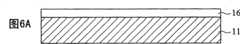
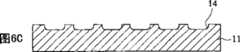
接着将参考图6A-6E说明本发明修整器的制造方法,图6A-6E显示如本发明第一实施例的修整器的制造方法。如图6A所示,首先提供一基板11,然后在基板11上形成一光阻层16,再以预先定义好的图案(未显示)去曝光、显影光阻层16,得到一形成有图案的光阻层16a,如图6B所示。接着如图6C,以湿蚀刻方法在基板11上形成碗形凹槽14,并去除光阻层16a,然后如图6D,将固着材料12填充到凹槽14中,最后,如图6E将磨粒13置放在固着材料12中,并进行真空硬焊,使固着材料12稳固地固着磨粒13与基板11。Next, the manufacturing method of the trimmer of the present invention will be described with reference to FIGS. 6A-6E , which show the manufacturing method of the trimmer according to the first embodiment of the present invention. As shown in FIG. 6A, a
在本发明修整器的制造方法中,形成上述凹槽的方法,并不局限于湿蚀刻,也可以采用雷射凿蚀(Laser Drill)、电铸(Galvono)或其它方式。In the manufacturing method of the trimmer of the present invention, the method of forming the groove is not limited to wet etching, and laser drilling (Laser Drill), electroforming (Galvono) or other methods may also be used.
本发明已以例证方式叙述说明,应了解上述的说明仅是描述性而非限制性。本领域技术人员可根据上述说明而为本发明的各种变更修改。While the present invention has been described by way of illustrations, it should be understood that the foregoing description is only descriptive and not restrictive. Those skilled in the art can make various changes and modifications of the present invention based on the above description.
Claims (17)
Priority Applications (1)
| Application Number | Priority Date | Filing Date | Title |
|---|---|---|---|
| CNA2005101028310ACN1931522A (en) | 2005-09-13 | 2005-09-13 | Dresser for dressing wafer polishing pad and manufacturing method thereof |
Applications Claiming Priority (1)
| Application Number | Priority Date | Filing Date | Title |
|---|---|---|---|
| CNA2005101028310ACN1931522A (en) | 2005-09-13 | 2005-09-13 | Dresser for dressing wafer polishing pad and manufacturing method thereof |
Publications (1)
| Publication Number | Publication Date |
|---|---|
| CN1931522Atrue CN1931522A (en) | 2007-03-21 |
Family
ID=37877620
Family Applications (1)
| Application Number | Title | Priority Date | Filing Date |
|---|---|---|---|
| CNA2005101028310APendingCN1931522A (en) | 2005-09-13 | 2005-09-13 | Dresser for dressing wafer polishing pad and manufacturing method thereof |
Country Status (1)
| Country | Link |
|---|---|
| CN (1) | CN1931522A (en) |
Cited By (9)
| Publication number | Priority date | Publication date | Assignee | Title |
|---|---|---|---|---|
| CN101726633B (en)* | 2008-10-16 | 2011-12-07 | 京元电子股份有限公司 | Test carrier plate with repairing layer |
| CN102092007B (en)* | 2009-12-11 | 2012-11-28 | 林舜天 | Preparation method of trimmer |
| CN101722475B (en)* | 2008-10-22 | 2013-03-06 | 宋健民 | CMP pad conditioner with hybrid abrasive surface and related methods |
| CN103192322A (en)* | 2012-01-06 | 2013-07-10 | 信越化学工业株式会社 | Dressing and manufacture of outer blade cutting wheel |
| CN104440516A (en)* | 2014-04-22 | 2015-03-25 | 上海华力微电子有限公司 | Grinding disk device |
| CN105612028A (en)* | 2013-08-07 | 2016-05-25 | 莱斯豪尔公司 | Dressing tool and method for the production thereof |
| CN107775193A (en)* | 2017-10-24 | 2018-03-09 | 长沙理工大学 | Method and system for brazing diamond by double-beam laser |
| CN110871407A (en)* | 2018-09-04 | 2020-03-10 | 宋健民 | Pad conditioner and method for chemical mechanical planarization |
| CN111775073A (en)* | 2020-06-19 | 2020-10-16 | 长江存储科技有限责任公司 | A polishing pad conditioner and method of making the same |
- 2005
- 2005-09-13CNCNA2005101028310Apatent/CN1931522A/enactivePending
Cited By (12)
| Publication number | Priority date | Publication date | Assignee | Title |
|---|---|---|---|---|
| CN101726633B (en)* | 2008-10-16 | 2011-12-07 | 京元电子股份有限公司 | Test carrier plate with repairing layer |
| CN101722475B (en)* | 2008-10-22 | 2013-03-06 | 宋健民 | CMP pad conditioner with hybrid abrasive surface and related methods |
| CN102092007B (en)* | 2009-12-11 | 2012-11-28 | 林舜天 | Preparation method of trimmer |
| CN103192322A (en)* | 2012-01-06 | 2013-07-10 | 信越化学工业株式会社 | Dressing and manufacture of outer blade cutting wheel |
| CN105612028A (en)* | 2013-08-07 | 2016-05-25 | 莱斯豪尔公司 | Dressing tool and method for the production thereof |
| CN104440516A (en)* | 2014-04-22 | 2015-03-25 | 上海华力微电子有限公司 | Grinding disk device |
| CN104440516B (en)* | 2014-04-22 | 2017-03-15 | 上海华力微电子有限公司 | A kind of grinding disc device |
| CN107775193A (en)* | 2017-10-24 | 2018-03-09 | 长沙理工大学 | Method and system for brazing diamond by double-beam laser |
| CN107775193B (en)* | 2017-10-24 | 2019-07-19 | 长沙理工大学 | Method and system for brazing diamond by double-beam laser |
| CN110871407A (en)* | 2018-09-04 | 2020-03-10 | 宋健民 | Pad conditioner and method for chemical mechanical planarization |
| CN111775073A (en)* | 2020-06-19 | 2020-10-16 | 长江存储科技有限责任公司 | A polishing pad conditioner and method of making the same |
| CN111775073B (en)* | 2020-06-19 | 2021-04-23 | 长江存储科技有限责任公司 | A polishing pad conditioner and method of making the same |
Similar Documents
| Publication | Publication Date | Title |
|---|---|---|
| TWI655057B (en) | Chemical mechanical polishing pad dresser | |
| JP3829092B2 (en) | Conditioner for polishing pad and method for producing the same | |
| KR101091030B1 (en) | Method for producing pad conditioner having reduced friction | |
| TW200837823A (en) | CMP pad conditioners and associated methods | |
| JP2007044863A (en) | Conditioner for wafer polishing pad and its manufacturing method | |
| TW200821092A (en) | Conditioning disk having uniform structures | |
| TWI537097B (en) | Composite conditioner and method for manufacturing the same and cmp application thereof | |
| CN109153106A (en) | Diamond Composite CMP Pad Conditioner | |
| WO2013012226A2 (en) | Cmp pad conditioner | |
| KR101052325B1 (en) | CMP pad conditioner and manufacturing method thereof | |
| CN1931522A (en) | Dresser for dressing wafer polishing pad and manufacturing method thereof | |
| CN106041741B (en) | A CMP polishing pad dresser with porous structure | |
| US20180354095A1 (en) | Grinding Tool and Method of Fabricating the Same | |
| US20030109204A1 (en) | Fixed abrasive CMP pad dresser and associated methods | |
| TWM446063U (en) | Chemical mechanical polishing pad dresser | |
| TWI602650B (en) | Retaining ring for chemical mechanical polishing | |
| CN110871407A (en) | Pad conditioner and method for chemical mechanical planarization | |
| JP4281253B2 (en) | Electrodeposition whetstone, manufacturing apparatus and manufacturing method thereof | |
| EP1779971A1 (en) | Pad conditioner for conditioning a CMP pad and method of making such a pad conditioner | |
| KR200175263Y1 (en) | The structure of the conditioner for CMP(Chemical Mechanical Polishing) Pad in CMP process | |
| CN106078516B (en) | A kind of CMP polishing pad dresser | |
| KR20210038216A (en) | Diamond Tip with Regular Array and Insert of Single Crystal Diamond | |
| CN212824753U (en) | Sapphire wafer and sapphire dresser for chemical mechanical polishing pad | |
| KR101103137B1 (en) | Pad conditioner and manufacturing method thereof | |
| TWI492291B (en) | Chemical mechanical polishing conditioner and method for fabricating the same |
Legal Events
| Date | Code | Title | Description |
|---|---|---|---|
| C06 | Publication | ||
| PB01 | Publication | ||
| C10 | Entry into substantive examination | ||
| SE01 | Entry into force of request for substantive examination | ||
| C02 | Deemed withdrawal of patent application after publication (patent law 2001) | ||
| WD01 | Invention patent application deemed withdrawn after publication |