CN1928801B - Position detection system using laser speckle - Google Patents
Position detection system using laser speckleDownload PDFInfo
- Publication number
- CN1928801B CN1928801BCN200610154101XACN200610154101ACN1928801BCN 1928801 BCN1928801 BCN 1928801BCN 200610154101X ACN200610154101X ACN 200610154101XACN 200610154101 ACN200610154101 ACN 200610154101ACN 1928801 BCN1928801 BCN 1928801B
- Authority
- CN
- China
- Prior art keywords
- electromagnetic radiation
- dielectric
- detection system
- sensor array
- speckle
- Prior art date
- Legal status (The legal status is an assumption and is not a legal conclusion. Google has not performed a legal analysis and makes no representation as to the accuracy of the status listed.)
- Expired - Fee Related
Links
Images


Classifications
- G—PHYSICS
- G06—COMPUTING OR CALCULATING; COUNTING
- G06F—ELECTRIC DIGITAL DATA PROCESSING
- G06F3/00—Input arrangements for transferring data to be processed into a form capable of being handled by the computer; Output arrangements for transferring data from processing unit to output unit, e.g. interface arrangements
- G06F3/01—Input arrangements or combined input and output arrangements for interaction between user and computer
- G06F3/03—Arrangements for converting the position or the displacement of a member into a coded form
- G06F3/041—Digitisers, e.g. for touch screens or touch pads, characterised by the transducing means
- G06F3/042—Digitisers, e.g. for touch screens or touch pads, characterised by the transducing means by opto-electronic means
- G—PHYSICS
- G06—COMPUTING OR CALCULATING; COUNTING
- G06F—ELECTRIC DIGITAL DATA PROCESSING
- G06F3/00—Input arrangements for transferring data to be processed into a form capable of being handled by the computer; Output arrangements for transferring data from processing unit to output unit, e.g. interface arrangements
- G06F3/01—Input arrangements or combined input and output arrangements for interaction between user and computer
- G06F3/03—Arrangements for converting the position or the displacement of a member into a coded form
- G06F3/041—Digitisers, e.g. for touch screens or touch pads, characterised by the transducing means
- G06F3/042—Digitisers, e.g. for touch screens or touch pads, characterised by the transducing means by opto-electronic means
- G06F3/0421—Digitisers, e.g. for touch screens or touch pads, characterised by the transducing means by opto-electronic means by interrupting or reflecting a light beam, e.g. optical touch-screen
- G—PHYSICS
- G06—COMPUTING OR CALCULATING; COUNTING
- G06F—ELECTRIC DIGITAL DATA PROCESSING
- G06F3/00—Input arrangements for transferring data to be processed into a form capable of being handled by the computer; Output arrangements for transferring data from processing unit to output unit, e.g. interface arrangements
- G06F3/01—Input arrangements or combined input and output arrangements for interaction between user and computer
- G06F3/03—Arrangements for converting the position or the displacement of a member into a coded form
- G06F3/041—Digitisers, e.g. for touch screens or touch pads, characterised by the transducing means
- G06F3/046—Digitisers, e.g. for touch screens or touch pads, characterised by the transducing means by electromagnetic means
- G—PHYSICS
- G06—COMPUTING OR CALCULATING; COUNTING
- G06F—ELECTRIC DIGITAL DATA PROCESSING
- G06F2203/00—Indexing scheme relating to G06F3/00 - G06F3/048
- G06F2203/041—Indexing scheme relating to G06F3/041 - G06F3/045
- G06F2203/04109—FTIR in optical digitiser, i.e. touch detection by frustrating the total internal reflection within an optical waveguide due to changes of optical properties or deformation at the touch location
Landscapes
- Engineering & Computer Science (AREA)
- General Engineering & Computer Science (AREA)
- Theoretical Computer Science (AREA)
- Physics & Mathematics (AREA)
- Human Computer Interaction (AREA)
- General Physics & Mathematics (AREA)
- Electromagnetism (AREA)
- Position Input By Displaying (AREA)
- Length Measuring Devices By Optical Means (AREA)
Abstract
Description
Technical field
The present invention relates to utilize the position detecting system of laser speckle.
Background technology
Point optional equipment (pointing device) is the Common Component of computer system, and by an optional equipment, the operator can come control computer with graphic user interface (GUI).For this purpose, develop various somes optional equipments for many years, comprised joystick, trace ball, mechanical mouse, light pen and optical mouse more in recent years.In addition, also have various types of digitizing tablets (tablet), they adopt writing pencil (stylus) usually.
The main target of these optional equipments is that the motion with operator's hand changes the operable signal of computing machine into.This can pass through display highlighting on the screen of computer monitor, and makes cursor move and realize in response to the motion of user's hand.The order that the user can select is corresponding with the position of cursor usually to link to each other.At first the motion by an optional equipment is with the tram of cursor positioning to the screen, and button or the switch on the optional equipment of trigger point can be selected the order of expecting thus then.
It is to obtain by joystick or mouse are detected with respect to the relative motion of fixed reference frame at first that position control is carried out in cursor positioning on the monitor screen, for mouse, described can be the end face or the mouse pad of desk with reference to reference frame.Technology commonly used is the ball that utilizes in the mouse, and described ball contacts with desktop or other surfaces when work, and rolls along with the motion of mouse.There are two rollers mouse inside, and they contact with ball and roll along with the rolling of ball.One of roller is orientated makes it to detect the motion that is nominally directions X, another roller orientation makes it relevant Y direction motion is detected for to become an angle of 90 degrees with first roller.These rollers are connected to independently axle, and each axle is connected to independently optical encoder, the electric signal that optical encoder output is corresponding with the motion of its corresponding roller.This signal is carried out suitable coding, and send to computing machine with the binary data form usually, computing machine is decoded to the signal of its reception, and makes the cursor on the computer screen move one section corresponding amount of the physical motion with mouse.
In recent years, adopted means of optical navigation technique to produce the motor message of indicating to along the relative motion of coordinate axis all directions.These technology for example are being used to replace traditional mouse and trace ball in the computer optics mouse, and are used for the position control of screen cursor in the used window user interface of computer system.This technology has some advantages, and comprising not needing moving component, described moving component accumulates dirt easily and is subjected to mechanical wear and destruction.
In the system that adopts means of optical navigation technique, motion is to measure by the relative motion of a series of images is followed the tracks of.At first, the two dimension view in reference surface zone is focused on the photodetector array, the output of photodetector is carried out digitizing and is stored as reference picture in the respective memory array.After one of short duration period, second image is carried out digitizing.If do not move, then the pattern of the pattern of the follow-up image that obtains of reference picture and reference picture is basic identical.On the other hand, if certain motion has taken place, then the pattern of successive image can be along the journal offset of moving, and the bias of pattern is corresponding to the amount of physical movement of photosensor array in the image.In computer system, replace the optical mouse that mechanical mouse is used for position control and adopted such technology.
In fact, the direction of motion of optical mouse and amount of exercise can be measured by a series of patterns through skew in the pattern of reference picture and second image are compared.The operation that is relative to each other between second image of reference picture and each skew, correct skew most probable produces maximum correlation value, comes to determine the migrated image of corresponding the best with the actual motion of optical mouse thus.Adopt said method can indicate the subsequent motion of optical mouse with successive image.Optical mouse sensor is to come work by a series of images that obtains the illuminated appearance feature in below.This surface has small external appearance characteristic.
Another kind of recent equipment is touch pad, and it is at first in order to be used for the laptop computer use and to develop.Touch pad is very sensitive for the contact of user's finger.They make the user only by at mobile finger tip on the touchpad surface cursor being moved on the computing machine plane.Whether exist the capacitance sensor array that is by the latticed layout in touchpad surface below to detect to user's finger tip.On computer screen cursor being navigated is to be coupled to sensor array by the finger tip capacitive with the user to come work.User's finger slides above sealing surfaces, and the sealing surfaces below is covered with two-layer trickle electric conductor, and two-layer electric conductor is arranged to latticed and produces surface field.Contacting this surface with finger tip can make the electric field at this some place produce distortion.By grid is scanned and each conductor of perception on the distortion degree, can to the contact finger tip position.This technology is a kind of form of capacitance sensing, is called field distortion (field distortion) sensing.The direction of mouse or cursor directly is subjected to the influence that people's finger tip moves on the screen on touchpad surface.Support software allows the acceleration customization to mouse, and gives that mouse " is clicked " and the function of " towing locks (drag-lock) ".The size of this touch pad is along with manufacturer and mould and change.Some is little of 2 inches * 2 inches.
Summary of the invention
A kind of detection system is disclosed in representative embodiment.Detection system comprises substrate, laser instrument and sensor array.Substrate comprises first surface, conceptually is divided into the second surface and the 3rd surface in a plurality of zones.Laser instrument is set to electromagnetic radiation to substrate, and electromagnetic radiation is incided on the zone of second surface subsequently.Sensor array is set to catch the electromagnetic radiation from the second surface reflection.If having first dielectric of first specific inductive capacity contacts with some zone, then incide the electromagnetic radiation experiences total internal reflection on it, if have second dielectric of second specific inductive capacity and other zones contact, then incide some electromagnetic radiation on it by in the second dielectric reflected back substrate.Sensor array is set to the laser speckle that the electromagnetic radiation of inciding the second surface place causes is detected, and the electromagnetic radiation from the reflection of second dielectric is detected.
In another kind of representative embodiment, a kind of method is disclosed.This method comprises uses the laser illumination surface, certain project is placed on lip-deep primary importance place, by first pattern of sensor array seizure by illuminated surface reflection, first pattern of catching is stored in the data memory device, this project is moved to lip-deep second place place, by second pattern of sensor array step, and compare with second pattern that captures by first pattern that will capture and to calculate the position change of this project with respect to primary importance by illuminated surface reflection.
According to following detailed description, in conjunction with the accompanying drawings, other aspects and the advantage of representative embodiment as herein described will be clearer.
Description of drawings
Accompanying drawing provides visual representation, can be used for more completely illustrating various representative embodiment, and can be used for understanding better they and inherent advantage thereof by those skilled in the art.In these accompanying drawings, identical label is represented corresponding ingredient.
Figure 1A is the synoptic diagram that incides the laser lighting light on the smooth reflecting surface.
Figure 1B is the synoptic diagram that incides on the reflecting surface with microscopic roughness, causes the laser lighting light of speckle.
Fig. 2 is the synoptic diagram of the detection system described in the various representative embodiment.
Fig. 3 is the surface described in the various representative embodiment from the view of looking with the angle of this surface quadrature.
Fig. 4 is another synoptic diagram of the detection system described in the various representative embodiment.
Fig. 5 is a process flow diagram of determining the method for position change described in the various representative embodiment with laser speckle.
Embodiment
As play shown in the accompanying drawing of example effect, herein disclosed is a kind of representative embodiment of novel position detecting system.Various guiders, for example joystick, trace ball, mechanical mouse, light pen, optical mouse and digitizing tablet have been used to drive the cursor on the computer screen.But in miniature electronic commodity (for example cell phone), mechanical rocker switch constitutes the main flow of present airmanship.It is that a side by pushing circular discs realizes that electric function specific, pre-programmed is selected.This technology is easy and have an efficiency-cost ratio.But, its four possible discrete rocking arm positions that selection dirigibility is limited in usually and miniscope is coupled (on/a following and left side/right side).In the representative embodiment of this paper, a kind of exquisiter navigation scheme is disclosed, wherein the detection with laser speckle combines with the motion of finger, drives cursor movement on the miniscope in the mode that is similar to computer mouse.
In detailed description below and a few width of cloth accompanying drawing, identical element comes mark with identical label.
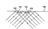
Figure 1A is the synoptic diagram that incides thelaser lighting light 110 on the smooth reflecting surface 120.From thelight 110 of laser instrument is relevant or homophase, and is also keeping like this from desirable smooth reflecting surface reflex time shown in Figure 1A.Reflect the ripple of gained shown inreflector laser 111 fromsmooth surface 120.
Figure 1B incides the synoptic diagram that causes thelaser lighting light 110 of speckle on the reflectingsurface 120 with microscopic roughness.But whenlaser 110 incided on thesurface 120 with microscopic roughness, shown in Figure 1B,part incident laser 110 produced light and shade " speckle " pattern bymicrodefect 121 scatterings, and this pattern can be detected by sensor array.This being scattered among Figure 1B represented byscattered light 112, is also referred to asspeckle light 112 herein.
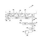
Fig. 2 is the synoptic diagram of thedetection system 200 described in the various representative embodiment.As shown in Figure 2,detection system 200 comprisessubstrate 210,laser instrument 220 and sensor array 230.Substrate 210 comprisesfirst surface 211,second surface 212 and the 3rd surface 213.Laser instrument 220 is set tolight 110, perhaps more generally,electromagnetic radiation 110 is transmitted in thesubstrate 210 byfirst surface 211, and describedlight 110 orelectromagnetic radiation 110 are incided on thesecond surface 212 subsequently.When first dielectric 250 with first specific inductive capacity contacts withsecond surface 212, launch with the collimated light beam form from thelight 110 oflaser instrument 220, and enter and pass throughsubstrate 210 along light path 240.In the case, the angle that the specific inductive capacity ofsubstrate 210 andlight 110 incide on thesecond surface 212 makeslight 110 be subjected to total internal reflection, does not almost havelight 110 to be lost in first dielectric 250.First dielectric 250 can be for example air or other suitable materials.In order to produce total internal reflection, the specific inductive capacity ofsubstrate 210 must be greater than the specific inductive capacity of first dielectric 250.
Light 110 advances to the3rd surface 213 after being reflected bysecond surface 212 immediately.The3rd surface 213 comprises 213a of first and second portion 213b.The 213a of first is a mirror surface type, makes to incide anyreflected light 111 on it all once more thereflected back substrate 210 from second surface 212.Sensor array 230 is set to receive thelight 110 on thesecond portion 213b that is mapped to the 3rd surface 213.Butdetection system 200 is typically designed to and makes do not having under the speckle and first dielectric 250 and the situation thatsecond surface 212 contacts, can not incide on thesecond portion 213b on the3rd surface 213 from thelight beam 110 of the light of laser instrument 220.But themicrodefect 121 among the 213a of first onmicrodefect 121 in thesecond surface 212 and the3rd surface 213 can make and receive somelight 110 on the sensor array 230.Like this,sensor array 230 is set tolight 110 caused laser speckle of incident onsecond surface 212 is detected, and to light 110 in incident/reflection of the 213a of first and detecting at the caused any laser speckle of the incident/reflection ofsecond surface 212 subsequently.
In addition, the 213a of first on the3rd surface 213 can comprise thefirst subdivision 213a-1 and the second subdivision 2131-2.Thefirst subdivision 213a-1 can be a mirror surface type, and thesecond subdivision 213a-2 can be other situation.For example, thesecond subdivision 213a-2 can by black or partly or entirely the other materials of absorbinglight 110 cover or apply, so that reduce to incide the ambient light on thesensor array 230, thereby make thescattered light 110 of 230 pairs of speckles of sensor array more responsive.Thesecond subdivision 213a-2 also can be transparent, makeslight 110 can penetrate substrate 210.Note, do not contain useful information by that part oflight 110 of speckle scattering,, then may makescattered light 110 be difficult to detect if allow them to be collected bysensor array 230 from having in thelaser instrument 220.
For the ease of diagram,microdefect 121 among themicrodefect 121 in thesecond surface 212, the 213a of first on the3rd surface 213 and thescattered light 112 that causes are not shown in Figure 2.
Fig. 3 is thesurface 212 described in the various representative embodiment from the view of observing with the angle of surperficial 212 quadratures.In Fig. 3, thesecond surface 212 that illustrates conceptually is divided into a plurality of regional 212m, for the ease of diagram, has only marked one of them equally.Should emphasize that a plurality ofzonule 212m are conceptual, just use for convenience of explanation.
Fig. 4 is another synoptic diagram of thedetection system 200 described in the various representative embodiment.In Fig. 4, second dielectric 260 contacts with partsecond surface 212, and second dielectric 260 can be ridge (ridge) or other the suitable material in finger, the fingerprint.Specifically, the one or more contact among a plurality of regional 212m of second dielectric 260 andsecond surface 212, first dielectric 250 contacts with all the other regional 212m ofsecond surface 212 simultaneously.Second dielectric 260 has fully greater than second specific inductive capacity of first specific inductive capacity, makes not experiences total internal reflection of those regional 212m of contacting with second dielectric 260 in the second surface 212.Result and Fig. 2 thatlaser 110 incides on those regional 212m that contact with first dielectric 250 in thesecond surface 212 are described the same.But for those zones that contact with second dielectric 260, reflectedlight 111 will change according to the speckle of second dielectric, 260 increases and the reflection characteristic of second dielectric 260.Therefore, exist under the situation of second dielectric 260 in one or more positions on thesecond surface 212, compare with the situation that does not have second dielectric 260, the optical pattern thatsensor array 230 receives can change.
Finish through before the whole process ofsubstrate 210,light 110 can one or many incides on thesecond surface 212 and by its reflection.Afterwards, this reflectedlight 111 can not reflected at the 3rd surperficial 213 places by the3rd surface 213 reflection one or many yet.Usually,second surface 212 can be parallel to the3rd surface 213,light 110 is provided with an end ofsensor array 230 as waveguide along substrate length direction guiding.Usually, several secondary reflections can take place atsecond surface 212 and the 3rd surperficial 213 places inlight 110.
In addition, the 213a of first on the3rd surface 213 can comprise thefirst subdivision 213a-1 and thesecond subdivision 213a-2.Thefirst subdivision 213a-1 can be a mirror surface type, and thesecond subdivision 213a-2 can be other situation.For example, thesecond subdivision 213a-2 can by black or partly or entirely the other materials of absorbinglight 110 cover or apply, so that reduce to incide the ambient light on thesensor array 230, thereby make thescattered light 110 of 230 pairs of speckles of sensor array more responsive.Thesecond subdivision 213a-2 also can be transparent, makeslight 110 can penetrate substrate 210.Note,,, then may makescattered light 110 be difficult to detect if allow them to be collected bysensor array 230 from not containing useful information in thelaser instrument 220 by that part oflight 110 speckle scattering and that do not reflect by second dielectric 260.
For the ease of diagram,microdefect 121 among themicrodefect 121 in thesecond surface 212, the 213a of first on the3rd surface 213 and thescattered light 112 that causes are not shown in Figure 4.
When work,, can detect of the relative motion of second dielectric 260 withsecond surface 212 finger tips by catching continuous image with sensor array 230.When second dielectric 260 is positioned at primary importance, to catch first pattern of gained and be sent tonavigation circuit 470, thecircuit 470 that navigates then is stored in it instorer 480 usually.Subsequently, second dielectric 260 moves to second place place with respect tosecond surface 212, produces second pattern different with first pattern owing to the position of second dielectric 260 is different.By comparing, can calculate the relative motion of second dielectric 260 bynavigation 470 pairs first patterns of circuit and second pattern.
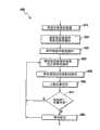
Fig. 5 is a process flow diagram of determining themethod 500 of position change described in the various representative embodiment with laser speckle.Atsquare frame 510 places, be used forlight 110illumination surface 212 from laser instrument 220.Square frame 510 forwards control tosquare frame 520 then.
Atsquare frame 520 places, the pattern that contains speckle bysensor array 230 is caught by 212 scatterings of illuminated surface is also referred to as speckle pattern herein.Square frame 520 forwards control tosquare frame 530 then.
Atsquare frame 530 places, the speckle pattern that captures is stored in the storer 480.Square frame 530 forwards control tosquare frame 540 then.
Atsquare frame 540 places, by the next speckle pattern ofsensor array 230 seizure by 212 scatterings of illuminated surface.Square frame 540 forwards control tosquare frame 550 then.
Atsquare frame 550 places, described next speckle pattern is stored in the storer 480.Square frame 550 forwards control tosquare frame 560 then.
Which kind of atsquare frame 560 places, two speckle pattern that capture are compared, to determine to have detected on thesurface 212 position change of project 260 (second dielectric 260).Square frame 560 forwards control tosquare frame 570 then.
Atsquare frame 570 places, if detected position change, thensquare frame 570 forwards control to square frame 580.Otherwisesquare frame 570 forwards control tosquare frame 540.
Atsquare frame 580 places, in response to the position change that calculates, themark 497 of doing exercises on the movingscreen 499, for example cursor 497.Square frame 580 forwards control tosquare frame 540 then.
Put it briefly, the invention discloses a kind of system, this system is used for the definite and navigation in position with laser speckle.In representative embodiment, that instruction disclosed herein can be used to provide is compact, system cheaply, and the motion that this system will point from the teeth outwards is used for above-mentioned purpose.Testing process has adopted the optical phenomena that is called laser speckle, and wherein, by the surface scattering with microscopic roughness, the reflected light of gained produces the pattern of bright dark speckle from the light that passes through the laser instrument that focuses on.
Light is from being coupled to the light emitted of waveguide, and detected by for example silicon sensor.The motion of finger at the waveguide surface top changes the optical pattern on the sensor.This change can be detected by sensor array.Waveguiding structure has some advantages.At first, it has reduced and the relevant eye-safe problem of laser output.Total internal reflection makes laser remain on waveguide (and module) inside, is in contact with it up to finger.Therefore laser only reflects and leaves finger, and can not leak into the waveguide outside.In addition, adopt waveguiding structure to increase the optical path length of process system.Optical path length has determined speckle size, and has therefore determined the pixel size that sensor array lists.Usually, the bigger speckle size of expectation can improve sensitivity like this so that the pixel size on the sensor is bigger.Waveguiding structure allows to increase optical path length under the situation that does not increase the module height, and this is very valuable usually in small-sized mobile application.
The speckle navigation is based on the coherent light interference technology, therefore needs LASER Light Source usually.The light of emission is coupled in the waveguide by prism structure.This structure can be integrated in the waveguide as Fig. 2 and (for example by injection-molded) shown in Figure 4, also can be separated.The light of direct emitted is through this structure and it is coupled out then, makes to small part light to be caught by sensor.In order to help this coupling, sensor can for example not linked waveguide by optical adhesive with not being with air gap.If finger or sundry item do not exist, perhaps point transfixion, then sensor can detect static speckle pattern.If finger motion, then the distribution pattern on the sensor also moves.This speckle pattern changes and can detect by sensor.Can compare by the pattern that two or more are caught speckle movement is detected.
The representative embodiment that this paper describes in detail by way of example rather than ways to restrain set forth.It will be appreciated by those skilled in the art that can carry out various changes to described embodiment in form and details, the equivalent embodiment that obtains still within the scope of the claims.
Claims (13)
1. detection system comprises:
Substrate, described substrate comprise first surface, are divided into the second surface in a plurality of zones and have first and the 3rd surface of second portion, and described second surface is parallel to described the 3rd surface;
Laser instrument, described laser instrument are set to electromagnetic radiation is transmitted in the described substrate through described first surface, and described electromagnetic radiation is incided on the described second surface subsequently; And
Sensor array, described sensor array is set to being caught by electromagnetic radiation reflection and that incide on the described second portion of described second surface, wherein, if having first dielectric of first specific inductive capacity contacts with described second surface, then incide the electromagnetic radiation experiences total internal reflection on the described second surface, if and second dielectric with second specific inductive capacity contacts with the part of described second surface, a part that then incides the electromagnetic radiation on the described part of described second surface is by in the described substrate of the described second dielectric reflected back, wherein, described first is set to the electromagnetic radiation of inciding on it is reflected at least in part, wherein said sensor array is set to the laser speckle that the described electromagnetic radiation of inciding described second surface place causes is detected, and the electromagnetic radiation by the reflection of described second dielectric detected
Described substrate is constructed such that the second portion that does not arrive described the 3rd surface because of the electromagnetic radiation of the described first dielectric experiences total internal reflection, described sensor array is oriented to only receive the electromagnetic radiation on the second portion that is mapped to described the 3rd surface, and
The first on described the 3rd surface comprises first subdivision and second subdivision, wherein, described first subdivision is the mirror surface type surface, described second subdivision covers or is coated with the material that can absorb described electromagnetic radiation, and described second subdivision is between the second portion on described first subdivision and described the 3rd surface.
2. detection system according to claim 1, wherein, except being produced the scattering by speckle, the described electromagnetic radiation of inciding on the zone that contacts with described first dielectric in the described second surface can not collected by described sensor array.
3. detection system according to claim 1, wherein, described laser instrument is a vertical cavity surface emitting laser.
4. detection system according to claim 1, wherein, described electromagnetic radiation incides on the described second surface at least twice, and incides on described the 3rd surface at least once.
5. detection system according to claim 1, wherein, described first dielectric is finger tissue or air.
6. detection system according to claim 1, wherein, described second dielectric is finger tissue or air.
7. detection system according to claim 1, wherein, described substrate conduct is from the used waveguide of the described electromagnetic radiation of described laser instrument.
8. detection system according to claim 1, wherein, described second dielectric comprises at least one ridge of finger.
9. detection system according to claim 1 also comprises:
Data memory device; With
The navigation circuit, wherein, described navigation circuit is set to collect signal from described sensor array, the described signal of collecting is stored in the described data memory device, and calculates of the motion of described second dielectric with respect to described second surface by the signal of collecting from different time points is compared.
10. detection system according to claim 9 also comprises:
Controller, wherein, positional information is sent to described controller as position signalling from described navigation circuit, and wherein, and described controller produces subsequently and can be used for output signal that the cursor on the screen is positioned.
11. determine to comprise the method for position change with the described detection system of claim 1 for one kind:
With the described second surface of described laser illumination;
Catch from the speckle pattern of illuminated described second surface reflection by described sensor array;
The described speckle pattern that captures is stored in the data memory device;
Catch from the follow-up speckle pattern of illuminated described second surface reflection by described sensor array; And
Compare by the speckle pattern that at least two are captured, calculating location changes.
12. method according to claim 11 also comprises:
If position change has taken place, then in response to the cursor on the described position change moving screen that calculates; And
From the follow-up speckle pattern of described seizure, repeat above-mentioned steps.
13. method according to claim 11, wherein, described speckle pattern comprises from the second dielectric speckle that contacts with described second surface.
Applications Claiming Priority (2)
| Application Number | Priority Date | Filing Date | Title |
|---|---|---|---|
| US11/222,257US7737959B2 (en) | 2005-09-08 | 2005-09-08 | Position detection system using laser speckle |
| US11/222,257 | 2005-09-08 |
Publications (2)
| Publication Number | Publication Date |
|---|---|
| CN1928801A CN1928801A (en) | 2007-03-14 |
| CN1928801Btrue CN1928801B (en) | 2011-09-14 |
Family
ID=37829604
Family Applications (1)
| Application Number | Title | Priority Date | Filing Date |
|---|---|---|---|
| CN200610154101XAExpired - Fee RelatedCN1928801B (en) | 2005-09-08 | 2006-09-08 | Position detection system using laser speckle |
Country Status (6)
| Country | Link |
|---|---|
| US (1) | US7737959B2 (en) |
| JP (1) | JP5166713B2 (en) |
| KR (1) | KR101192909B1 (en) |
| CN (1) | CN1928801B (en) |
| DE (1) | DE102006041815A1 (en) |
| TW (1) | TWI393030B (en) |
Families Citing this family (70)
| Publication number | Priority date | Publication date | Assignee | Title |
|---|---|---|---|---|
| US8610675B2 (en) | 2007-03-14 | 2013-12-17 | Power2B, Inc. | Interactive devices |
| US9317170B2 (en)* | 2005-05-18 | 2016-04-19 | Power2B, Inc. | Interactive devices |
| US10452207B2 (en) | 2005-05-18 | 2019-10-22 | Power2B, Inc. | Displays and information input devices |
| EP1907918A2 (en)* | 2005-07-05 | 2008-04-09 | O-Pen ApS | A touch pad system |
| CN101390223B (en)* | 2005-10-24 | 2012-02-01 | 劳伦斯利弗莫尔国家安全有限公司 | Photoactivated silicon carbide high voltage switch |
| US8013845B2 (en)* | 2005-12-30 | 2011-09-06 | Flatfrog Laboratories Ab | Optical touch pad with multilayer waveguide |
| US8094136B2 (en)* | 2006-07-06 | 2012-01-10 | Flatfrog Laboratories Ab | Optical touchpad with three-dimensional position determination |
| US8031186B2 (en)* | 2006-07-06 | 2011-10-04 | Flatfrog Laboratories Ab | Optical touchpad system and waveguide for use therein |
| US9063617B2 (en)* | 2006-10-16 | 2015-06-23 | Flatfrog Laboratories Ab | Interactive display system, tool for use with the system, and tool management apparatus |
| US20080189046A1 (en)* | 2007-02-02 | 2008-08-07 | O-Pen A/S | Optical tool with dynamic electromagnetic radiation and a system and method for determining the position and/or motion of an optical tool |
| US8400409B1 (en)* | 2007-07-10 | 2013-03-19 | Cypress Semiconductor Corporation | User interface devices, methods, and computer readable media for sensing movement of an actuator across a surface of a window |
| RU2519392C2 (en)* | 2008-01-11 | 2014-06-10 | О-Нэт Вэйв Тач Лимитед | Sensor device |
| US8031176B1 (en) | 2008-01-22 | 2011-10-04 | Cypress Semiconductor Corporation | Optical navigation system using a single-package motion sensor |
| WO2009114821A2 (en)* | 2008-03-14 | 2009-09-17 | Cypress Semiconductor | Apparatus and method of finger-motion based navigation using optical sensing |
| TW201013492A (en)* | 2008-06-23 | 2010-04-01 | Flatfrog Lab Ab | Determining the location of one or more objects on a touch surface |
| TW201007530A (en)* | 2008-06-23 | 2010-02-16 | Flatfrog Lab Ab | Detecting the location of an object on a touch surface |
| WO2010006885A2 (en)* | 2008-06-23 | 2010-01-21 | Flatfrog Laboratories Ab | Detecting the location of an object on a touch surface |
| TW201005606A (en)* | 2008-06-23 | 2010-02-01 | Flatfrog Lab Ab | Detecting the locations of a plurality of objects on a touch surface |
| TW201001258A (en)* | 2008-06-23 | 2010-01-01 | Flatfrog Lab Ab | Determining the location of one or more objects on a touch surface |
| WO2010006348A1 (en)* | 2008-07-15 | 2010-01-21 | Isiqiri Interface Technologies Gmbh | Control surface for a data processing system |
| US8237684B2 (en)* | 2008-09-26 | 2012-08-07 | Avago Technologies Ecbu Ip (Singapore) Pte. Ltd. | User input device with planar light guide illumination plate |
| SE533704C2 (en) | 2008-12-05 | 2010-12-07 | Flatfrog Lab Ab | Touch sensitive apparatus and method for operating the same |
| US8711121B2 (en)* | 2008-12-12 | 2014-04-29 | Wacom Co., Ltd. | Architecture and method for multi-aspect touchscreen scanning |
| AT507702B1 (en)* | 2009-01-07 | 2013-07-15 | Isiqiri Interface Tech Gmbh | DETECTOR AREA |
| US8089466B2 (en)* | 2009-02-18 | 2012-01-03 | Avago Technologies Ecbu Ip (Singapore) Pte. Ltd. | System and method for performing optical navigation using a compact optical element |
| JP4902714B2 (en)* | 2009-09-30 | 2012-03-21 | シャープ株式会社 | Optical pointing device, electronic apparatus including the same, light guide, and light guide method. |
| CN102053761A (en)* | 2009-10-29 | 2011-05-11 | 北京汇冠新技术股份有限公司 | Touch screen and touch system |
| US8358282B2 (en)* | 2009-12-18 | 2013-01-22 | Avago Technologies Ecbu Ip (Singapore) Pte. Ltd. | Object detection device |
| CN101751186B (en)* | 2009-12-30 | 2011-12-21 | 鸿富锦精密工业(深圳)有限公司 | Touch electronic device and control method thereof |
| ES2617442T3 (en) | 2010-01-04 | 2017-06-19 | O-Net Wavetouch Limited | Device and procedure to detect the presence of an object |
| JP4902768B2 (en)* | 2010-05-11 | 2012-03-21 | シャープ株式会社 | Optical pointing device and electronic apparatus equipped with the same |
| GB201014053D0 (en)* | 2010-08-23 | 2010-10-06 | St Microelectronics Res & Dev | Optical navigation device |
| US8546741B2 (en)* | 2011-01-13 | 2013-10-01 | Avago Technologies General Ip (Singapore) Pte. Ltd. | Compact optical finger navigation system based on speckles with an optical element including an optical redirection surface |
| TW201234026A (en)* | 2011-02-01 | 2012-08-16 | Chang Yu Technology Co Ltd | Inspection system of photo-link light receiver and method thereof |
| CN102959494B (en) | 2011-06-16 | 2017-05-17 | 赛普拉斯半导体公司 | An optical navigation module with capacitive sensor |
| US8896553B1 (en) | 2011-11-30 | 2014-11-25 | Cypress Semiconductor Corporation | Hybrid sensor module |
| US9880653B2 (en) | 2012-04-30 | 2018-01-30 | Corning Incorporated | Pressure-sensing touch system utilizing total-internal reflection |
| US10168835B2 (en) | 2012-05-23 | 2019-01-01 | Flatfrog Laboratories Ab | Spatial resolution in touch displays |
| US9804777B1 (en) | 2012-10-23 | 2017-10-31 | Google Inc. | Gesture-based text selection |
| US10019113B2 (en) | 2013-04-11 | 2018-07-10 | Flatfrog Laboratories Ab | Tomographic processing for touch detection |
| WO2015005847A1 (en) | 2013-07-12 | 2015-01-15 | Flatfrog Laboratories Ab | Partial detect mode |
| US10203759B1 (en)* | 2013-08-19 | 2019-02-12 | Maxim Integrated Products, Inc. | Gesture detection device having an angled light collimating structure |
| US9366565B2 (en)* | 2013-08-26 | 2016-06-14 | Flatfrog Laboratories Ab | Light out-coupling arrangement and a touch sensitive system comprising the out-coupling arrangement |
| US10146376B2 (en) | 2014-01-16 | 2018-12-04 | Flatfrog Laboratories Ab | Light coupling in TIR-based optical touch systems |
| WO2015108480A1 (en) | 2014-01-16 | 2015-07-23 | Flatfrog Laboratories Ab | Improvements in tir-based optical touch systems of projection-type |
| EP3161594A4 (en) | 2014-06-27 | 2018-01-17 | FlatFrog Laboratories AB | Detection of surface contamination |
| US10318077B2 (en) | 2014-09-05 | 2019-06-11 | Hewlett-Packard Development Company, L.P. | Coherent illumination for touch point identification |
| EP3250993B1 (en) | 2015-01-28 | 2019-09-04 | FlatFrog Laboratories AB | Dynamic touch quarantine frames |
| US10318074B2 (en) | 2015-01-30 | 2019-06-11 | Flatfrog Laboratories Ab | Touch-sensing OLED display with tilted emitters |
| US10496227B2 (en) | 2015-02-09 | 2019-12-03 | Flatfrog Laboratories Ab | Optical touch system comprising means for projecting and detecting light beams above and inside a transmissive panel |
| US10401546B2 (en) | 2015-03-02 | 2019-09-03 | Flatfrog Laboratories Ab | Optical component for light coupling |
| EP4075246B1 (en) | 2015-12-09 | 2024-07-03 | FlatFrog Laboratories AB | Stylus for optical touch system |
| CN105630206B (en)* | 2015-12-23 | 2018-10-16 | 广州中国科学院先进技术研究所 | A kind of touch localization method and system based on DIC |
| WO2017176781A1 (en) | 2016-04-06 | 2017-10-12 | Laser Associated Sciences, LLC | System for blood flow measurement with affixed laser speckle contrast analysis |
| EP3545392A4 (en) | 2016-11-24 | 2020-07-29 | FlatFrog Laboratories AB | AUTOMATIC OPTIMIZATION OF TOUCH SIGNALS |
| KR20250020732A (en) | 2016-12-07 | 2025-02-11 | 플라트프로그 라보라토리즈 에이비 | An improved touch device |
| CN110300950B (en) | 2017-02-06 | 2023-06-16 | 平蛙实验室股份公司 | Optical coupling in touch sensing systems |
| CN106802658B (en)* | 2017-03-21 | 2019-09-20 | 厦门大学 | A fully automatic high-precision indoor rapid positioning method |
| US10606414B2 (en) | 2017-03-22 | 2020-03-31 | Flatfrog Laboratories Ab | Eraser for touch displays |
| EP4036697A1 (en) | 2017-03-28 | 2022-08-03 | FlatFrog Laboratories AB | Optical touch sensing apparatus |
| US11256371B2 (en) | 2017-09-01 | 2022-02-22 | Flatfrog Laboratories Ab | Optical component |
| CN108007352B (en)* | 2018-01-05 | 2024-03-15 | 洛阳理工学院 | Foot stress measuring device based on digital speckle correlation technology |
| DE102018200566B4 (en)* | 2018-01-15 | 2021-07-15 | Fraunhofer-Gesellschaft zur Förderung der angewandten Forschung e.V. | System and method for monitoring the manufacturing accuracy in the additive manufacturing of three-dimensional components |
| WO2019172826A1 (en) | 2018-03-05 | 2019-09-12 | Flatfrog Laboratories Ab | Improved touch-sensing apparatus |
| WO2020080992A1 (en) | 2018-10-20 | 2020-04-23 | Flatfrog Laboratories Ab | Frame for a touch-sensitive device and tool therefor |
| WO2020153890A1 (en) | 2019-01-25 | 2020-07-30 | Flatfrog Laboratories Ab | A videoconferencing terminal and method of operating the same |
| ES2991658T3 (en) | 2019-11-25 | 2024-12-04 | Flatfrog Lab Ab | A touch device |
| US12282653B2 (en) | 2020-02-08 | 2025-04-22 | Flatfrog Laboratories Ab | Touch apparatus with low latency interactions |
| US11893189B2 (en) | 2020-02-10 | 2024-02-06 | Flatfrog Laboratories Ab | Touch-sensing apparatus |
| CN114413750B (en)* | 2021-12-01 | 2023-09-15 | 广西交科集团有限公司 | Positioning sensor, positioning system and positioning method based on laser scattering light spots |
Citations (4)
| Publication number | Priority date | Publication date | Assignee | Title |
|---|---|---|---|---|
| US4728186A (en)* | 1985-03-03 | 1988-03-01 | Fujitsu Limited | Uneven-surface data detection apparatus |
| US5914709A (en)* | 1997-03-14 | 1999-06-22 | Poa Sana, Llc | User input device for a computer system |
| US6816537B2 (en)* | 2001-10-09 | 2004-11-09 | Koninklijke Philips Electronics N.V. | Device having touch sensitivity functionality |
| CN1659501A (en)* | 2002-06-04 | 2005-08-24 | 皇家飞利浦电子股份有限公司 | Method of measuring the movement of an input device |
Family Cites Families (18)
| Publication number | Priority date | Publication date | Assignee | Title |
|---|---|---|---|---|
| US3716301A (en)* | 1971-03-17 | 1973-02-13 | Sperry Rand Corp | Fingerprint identification apparatus |
| JPS5378731A (en)* | 1976-12-22 | 1978-07-12 | Nec Corp | Keyboard with preference output control |
| US4794384A (en)* | 1984-09-27 | 1988-12-27 | Xerox Corporation | Optical translator device |
| AUPN802296A0 (en)* | 1996-02-12 | 1996-03-07 | Fingerscan Pty Limited | An input device for controlling a pointer on the screen of a computer |
| TR199901910T2 (en)* | 1997-02-12 | 1999-10-21 | Kanitech A/S | A device used to enter data into a computer |
| SG120889A1 (en)* | 2001-09-28 | 2006-04-26 | Semiconductor Energy Lab | A light emitting device and electronic apparatus using the same |
| AU2003208566A1 (en)* | 2003-01-08 | 2004-08-10 | Explay Ltd. | An image projecting device and method |
| CN1244044C (en)* | 2003-01-20 | 2006-03-01 | 张宏志 | Mouse optical signal treatment method and device |
| US7274808B2 (en) | 2003-04-18 | 2007-09-25 | Avago Technologies Ecbu Ip (Singapore)Pte Ltd | Imaging system and apparatus for combining finger recognition and finger navigation |
| US7164782B2 (en)* | 2003-04-18 | 2007-01-16 | Avago Technologies Ecbu Ip (Singapore) Pte. Ltd. | System and method for time-space multiplexing in finger-imaging applications |
| TWI253017B (en)* | 2003-05-16 | 2006-04-11 | Agilent Technologies Inc | Low power consumption, broad navigability optical mouse |
| US7321359B2 (en)* | 2003-07-30 | 2008-01-22 | Avago Technologies Ecbu Ip (Singapore) Pte. Ltd. | Method and device for optical navigation |
| JP2007506178A (en)* | 2003-09-22 | 2007-03-15 | コニンクリユケ フィリップス エレクトロニクス エヌ.ブイ. | Light touch screen |
| WO2005050748A1 (en)* | 2003-11-19 | 2005-06-02 | Nichia Corporation | Semiconductor device and method for manufacturing same |
| TWI258704B (en)* | 2004-01-16 | 2006-07-21 | Avago Tech Ecbu Ip Sg Pte Ltd | Method and system for optically tracking a target using an interferometric technique |
| JP3895730B2 (en)* | 2004-01-26 | 2007-03-22 | 株式会社リケン | Method and apparatus for detecting direction of member whose outer periphery is vertically asymmetrical |
| JP2005235567A (en)* | 2004-02-19 | 2005-09-02 | Seiko Epson Corp | ORGANIC EL DEVICE, ITS MANUFACTURING METHOD, AND ELECTRONIC DEVICE |
| JP2006209802A (en)* | 2006-04-12 | 2006-08-10 | Kiichiro Kurokawa | Hand-held controller |
- 2005
- 2005-09-08USUS11/222,257patent/US7737959B2/enactiveActive
- 2006
- 2006-08-30TWTW095131960Apatent/TWI393030B/enactive
- 2006-09-06DEDE102006041815Apatent/DE102006041815A1/ennot_activeCeased
- 2006-09-06JPJP2006241609Apatent/JP5166713B2/enactiveActive
- 2006-09-07KRKR1020060086053Apatent/KR101192909B1/ennot_activeExpired - Fee Related
- 2006-09-08CNCN200610154101XApatent/CN1928801B/ennot_activeExpired - Fee Related
Patent Citations (4)
| Publication number | Priority date | Publication date | Assignee | Title |
|---|---|---|---|---|
| US4728186A (en)* | 1985-03-03 | 1988-03-01 | Fujitsu Limited | Uneven-surface data detection apparatus |
| US5914709A (en)* | 1997-03-14 | 1999-06-22 | Poa Sana, Llc | User input device for a computer system |
| US6816537B2 (en)* | 2001-10-09 | 2004-11-09 | Koninklijke Philips Electronics N.V. | Device having touch sensitivity functionality |
| CN1659501A (en)* | 2002-06-04 | 2005-08-24 | 皇家飞利浦电子股份有限公司 | Method of measuring the movement of an input device |
Also Published As
| Publication number | Publication date |
|---|---|
| US20070052684A1 (en) | 2007-03-08 |
| TW200717287A (en) | 2007-05-01 |
| KR20070029073A (en) | 2007-03-13 |
| JP2007073051A (en) | 2007-03-22 |
| DE102006041815A1 (en) | 2007-03-29 |
| TWI393030B (en) | 2013-04-11 |
| CN1928801A (en) | 2007-03-14 |
| KR101192909B1 (en) | 2012-10-18 |
| JP5166713B2 (en) | 2013-03-21 |
| US7737959B2 (en) | 2010-06-15 |
Similar Documents
| Publication | Publication Date | Title |
|---|---|---|
| CN1928801B (en) | Position detection system using laser speckle | |
| US7295329B2 (en) | Position detection system | |
| KR100465969B1 (en) | Pointing device using the surface of a finger | |
| US7313255B2 (en) | System and method for optically detecting a click event | |
| JP4392377B2 (en) | Optical device that measures the distance between the device and the surface | |
| CN1175344C (en) | pen computer pointing device | |
| US8022928B2 (en) | Free-space pointing and handwriting | |
| EP1164538A2 (en) | Pointing device having rotational sensing mechanisms | |
| EP1591880B1 (en) | Data input devices and methods for detecting movement of a tracking surface by a speckle pattern | |
| KR100399635B1 (en) | Optical mouse | |
| US20080030458A1 (en) | Inertial input apparatus and method with optical motion state detection | |
| JP2004318892A (en) | Spatio-temporal multiplexing system and method for finger image input application | |
| KR100905382B1 (en) | Method for processing optical signals in a computer mouse | |
| JP2006202291A (en) | Optical slide pad | |
| US20070139381A1 (en) | Speckle navigation system | |
| US20070241262A1 (en) | Optical sensing unit for an optical input device | |
| CN1331032C (en) | Pen-shaped optical mouse | |
| US7199791B2 (en) | Pen mouse | |
| CN114415848A (en) | Mouse with touch area | |
| US7714843B1 (en) | Computer input device with a self-contained camera | |
| JP2015515672A (en) | Computer system and control method thereof | |
| JPH0638224B2 (en) | Optical translator device | |
| CN2660590Y (en) | pointer input device | |
| JP2000200144A (en) | Optical mouse | |
| KR20070021068A (en) | Optical navigation device and how to generate navigation information |
Legal Events
| Date | Code | Title | Description |
|---|---|---|---|
| C06 | Publication | ||
| PB01 | Publication | ||
| C10 | Entry into substantive examination | ||
| SE01 | Entry into force of request for substantive examination | ||
| C14 | Grant of patent or utility model | ||
| GR01 | Patent grant | ||
| ASS | Succession or assignment of patent right | Owner name:AVAGO TECHNOLOGIES GENERAL IP (SINGAPORE) CORPORAT Free format text:FORMER OWNER: AVAGO TECHNOLOGIES ECBU IP (SINGAPORE) PTE. LTD. Effective date:20130514 | |
| C41 | Transfer of patent application or patent right or utility model | ||
| TR01 | Transfer of patent right | Effective date of registration:20130514 Address after:Singapore Singapore Patentee after:Avago Technologies General IP (Singapore) Pte. Ltd. Address before:Singapore Singapore Patentee before:ANHUA HIGH TECHNOLOGY ECBUIP (SINGAPORE) PRIVATE Ltd. | |
| C41 | Transfer of patent application or patent right or utility model | ||
| TR01 | Transfer of patent right | Effective date of registration:20161013 Address after:Chinese Taiwan New Taipei City Patentee after:PixArt Imaging Inc. Address before:Singapore Singapore Patentee before:Avago Technologies General IP (Singapore) Pte. Ltd. | |
| CF01 | Termination of patent right due to non-payment of annual fee | Granted publication date:20110914 | |
| CF01 | Termination of patent right due to non-payment of annual fee |