CN1921159B - Light source with UV LED and UV reflector - Google Patents
Light source with UV LED and UV reflectorDownload PDFInfo
- Publication number
- CN1921159B CN1921159BCN2006101114626ACN200610111462ACN1921159BCN 1921159 BCN1921159 BCN 1921159BCN 2006101114626 ACN2006101114626 ACN 2006101114626ACN 200610111462 ACN200610111462 ACN 200610111462ACN 1921159 BCN1921159 BCN 1921159B
- Authority
- CN
- China
- Prior art keywords
- light
- phosphor layer
- phosphor
- ultraviolet
- source
- Prior art date
- Legal status (The legal status is an assumption and is not a legal conclusion. Google has not performed a legal analysis and makes no representation as to the accuracy of the status listed.)
- Expired - Fee Related
Links
- OAICVXFJPJFONN-UHFFFAOYSA-NPhosphorusChemical compound[P]OAICVXFJPJFONN-UHFFFAOYSA-N0.000claimsabstractdescription78
- 230000005855radiationEffects0.000claimsabstractdescription22
- 239000004065semiconductorSubstances0.000claimsabstractdescription22
- 239000000463materialSubstances0.000claimsdescription19
- 238000000034methodMethods0.000claimsdescription18
- 239000004593EpoxySubstances0.000claimsdescription9
- 238000005538encapsulationMethods0.000claimsdescription6
- 239000008393encapsulating agentSubstances0.000claimsdescription5
- 239000002223garnetSubstances0.000claimsdescription3
- BPQQTUXANYXVAA-UHFFFAOYSA-NOrthosilicateChemical compound[O-][Si]([O-])([O-])[O-]BPQQTUXANYXVAA-UHFFFAOYSA-N0.000claims4
- 239000004904UV filterSubstances0.000claims3
- NINIDFKCEFEMDL-UHFFFAOYSA-NSulfurChemical compound[S]NINIDFKCEFEMDL-UHFFFAOYSA-N0.000claims2
- 238000001914filtrationMethods0.000claims2
- 150000004767nitridesChemical class0.000claims2
- 229920001296polysiloxanePolymers0.000claims2
- 239000003566sealing materialSubstances0.000claims2
- 150000003346selenoethersChemical class0.000claims2
- 229910052717sulfurInorganic materials0.000claims2
- 239000011593sulfurSubstances0.000claims2
- 238000007789sealingMethods0.000claims1
- 239000010409thin filmSubstances0.000abstractdescription2
- 230000008901benefitEffects0.000description5
- 229910019990cerium-doped yttrium aluminum garnetInorganic materials0.000description4
- 239000003086colorantSubstances0.000description4
- 239000011248coating agentSubstances0.000description3
- 238000000576coating methodMethods0.000description3
- 230000005284excitationEffects0.000description3
- 238000004020luminiscence typeMethods0.000description3
- 238000001228spectrumMethods0.000description3
- 229910019655synthetic inorganic crystalline materialInorganic materials0.000description3
- 229910002601GaNInorganic materials0.000description2
- 230000015556catabolic processEffects0.000description2
- 239000013078crystalSubstances0.000description2
- 238000000151depositionMethods0.000description2
- 239000002019doping agentSubstances0.000description2
- 230000000694effectsEffects0.000description2
- 238000005286illuminationMethods0.000description2
- WABPQHHGFIMREM-FTXFMUIASA-Nlead-202Chemical compound[202Pb]WABPQHHGFIMREM-FTXFMUIASA-N0.000description2
- 239000000203mixtureSubstances0.000description2
- 230000008569processEffects0.000description2
- -1rare earth compoundChemical class0.000description2
- 229910052761rare earth metalInorganic materials0.000description2
- 238000002310reflectometryMethods0.000description2
- 239000000126substanceSubstances0.000description2
- 229910052684CeriumInorganic materials0.000description1
- GYHNNYVSQQEPJS-UHFFFAOYSA-NGalliumChemical compound[Ga]GYHNNYVSQQEPJS-UHFFFAOYSA-N0.000description1
- JMASRVWKEDWRBT-UHFFFAOYSA-NGallium nitrideChemical compound[Ga]#NJMASRVWKEDWRBT-UHFFFAOYSA-N0.000description1
- 230000004075alterationEffects0.000description1
- JNDMLEXHDPKVFC-UHFFFAOYSA-Naluminum;oxygen(2-);yttrium(3+)Chemical compound[O-2].[O-2].[O-2].[Al+3].[Y+3]JNDMLEXHDPKVFC-UHFFFAOYSA-N0.000description1
- 238000013459approachMethods0.000description1
- NWAIGJYBQQYSPW-UHFFFAOYSA-NazanylidyneindiganeChemical compound[In]#NNWAIGJYBQQYSPW-UHFFFAOYSA-N0.000description1
- 239000011230binding agentSubstances0.000description1
- ZMIGMASIKSOYAM-UHFFFAOYSA-NceriumChemical compound[Ce][Ce][Ce][Ce][Ce][Ce][Ce][Ce][Ce][Ce][Ce][Ce][Ce][Ce][Ce][Ce][Ce][Ce][Ce][Ce][Ce][Ce][Ce][Ce][Ce][Ce][Ce][Ce][Ce][Ce][Ce][Ce][Ce][Ce][Ce][Ce][Ce][Ce]ZMIGMASIKSOYAM-UHFFFAOYSA-N0.000description1
- 238000006243chemical reactionMethods0.000description1
- 230000000295complement effectEffects0.000description1
- 238000006731degradation reactionMethods0.000description1
- 230000008021depositionEffects0.000description1
- 238000005401electroluminescenceMethods0.000description1
- 238000001839endoscopyMethods0.000description1
- 238000005516engineering processMethods0.000description1
- 239000003822epoxy resinSubstances0.000description1
- 238000011156evaluationMethods0.000description1
- 229910052733galliumInorganic materials0.000description1
- 230000003760hair shineEffects0.000description1
- WABPQHHGFIMREM-OIOBTWANSA-Nlead-204Chemical compound[204Pb]WABPQHHGFIMREM-OIOBTWANSA-N0.000description1
- 238000001748luminescence spectrumMethods0.000description1
- 238000004519manufacturing processMethods0.000description1
- 238000005297material degradation processMethods0.000description1
- 239000011159matrix materialSubstances0.000description1
- 230000007246mechanismEffects0.000description1
- 238000012986modificationMethods0.000description1
- 230000004048modificationEffects0.000description1
- 229920000647polyepoxidePolymers0.000description1
- 239000000843powderSubstances0.000description1
- 238000009877renderingMethods0.000description1
- 230000003595spectral effectEffects0.000description1
- 238000001356surgical procedureMethods0.000description1
- 238000001429visible spectrumMethods0.000description1
- 229910019901yttrium aluminum garnetInorganic materials0.000description1
Images

Classifications
- H—ELECTRICITY
- H10—SEMICONDUCTOR DEVICES; ELECTRIC SOLID-STATE DEVICES NOT OTHERWISE PROVIDED FOR
- H10H—INORGANIC LIGHT-EMITTING SEMICONDUCTOR DEVICES HAVING POTENTIAL BARRIERS
- H10H20/00—Individual inorganic light-emitting semiconductor devices having potential barriers, e.g. light-emitting diodes [LED]
- H10H20/80—Constructional details
- H10H20/85—Packages
- H10H20/851—Wavelength conversion means
- H10H20/8515—Wavelength conversion means not being in contact with the bodies
- H—ELECTRICITY
- H10—SEMICONDUCTOR DEVICES; ELECTRIC SOLID-STATE DEVICES NOT OTHERWISE PROVIDED FOR
- H10H—INORGANIC LIGHT-EMITTING SEMICONDUCTOR DEVICES HAVING POTENTIAL BARRIERS
- H10H20/00—Individual inorganic light-emitting semiconductor devices having potential barriers, e.g. light-emitting diodes [LED]
- H10H20/80—Constructional details
- H10H20/84—Coatings, e.g. passivation layers or antireflective coatings
- H10H20/841—Reflective coatings, e.g. dielectric Bragg reflectors
- H—ELECTRICITY
- H01—ELECTRIC ELEMENTS
- H01L—SEMICONDUCTOR DEVICES NOT COVERED BY CLASS H10
- H01L2224/00—Indexing scheme for arrangements for connecting or disconnecting semiconductor or solid-state bodies and methods related thereto as covered by H01L24/00
- H01L2224/01—Means for bonding being attached to, or being formed on, the surface to be connected, e.g. chip-to-package, die-attach, "first-level" interconnects; Manufacturing methods related thereto
- H01L2224/42—Wire connectors; Manufacturing methods related thereto
- H01L2224/47—Structure, shape, material or disposition of the wire connectors after the connecting process
- H01L2224/48—Structure, shape, material or disposition of the wire connectors after the connecting process of an individual wire connector
- H01L2224/4805—Shape
- H01L2224/4809—Loop shape
- H01L2224/48091—Arched
- H—ELECTRICITY
- H01—ELECTRIC ELEMENTS
- H01L—SEMICONDUCTOR DEVICES NOT COVERED BY CLASS H10
- H01L2224/00—Indexing scheme for arrangements for connecting or disconnecting semiconductor or solid-state bodies and methods related thereto as covered by H01L24/00
- H01L2224/01—Means for bonding being attached to, or being formed on, the surface to be connected, e.g. chip-to-package, die-attach, "first-level" interconnects; Manufacturing methods related thereto
- H01L2224/42—Wire connectors; Manufacturing methods related thereto
- H01L2224/47—Structure, shape, material or disposition of the wire connectors after the connecting process
- H01L2224/48—Structure, shape, material or disposition of the wire connectors after the connecting process of an individual wire connector
- H01L2224/481—Disposition
- H01L2224/48151—Connecting between a semiconductor or solid-state body and an item not being a semiconductor or solid-state body, e.g. chip-to-substrate, chip-to-passive
- H01L2224/48221—Connecting between a semiconductor or solid-state body and an item not being a semiconductor or solid-state body, e.g. chip-to-substrate, chip-to-passive the body and the item being stacked
- H01L2224/48245—Connecting between a semiconductor or solid-state body and an item not being a semiconductor or solid-state body, e.g. chip-to-substrate, chip-to-passive the body and the item being stacked the item being metallic
- H01L2224/48247—Connecting between a semiconductor or solid-state body and an item not being a semiconductor or solid-state body, e.g. chip-to-substrate, chip-to-passive the body and the item being stacked the item being metallic connecting the wire to a bond pad of the item
- H—ELECTRICITY
- H01—ELECTRIC ELEMENTS
- H01L—SEMICONDUCTOR DEVICES NOT COVERED BY CLASS H10
- H01L2224/00—Indexing scheme for arrangements for connecting or disconnecting semiconductor or solid-state bodies and methods related thereto as covered by H01L24/00
- H01L2224/01—Means for bonding being attached to, or being formed on, the surface to be connected, e.g. chip-to-package, die-attach, "first-level" interconnects; Manufacturing methods related thereto
- H01L2224/42—Wire connectors; Manufacturing methods related thereto
- H01L2224/47—Structure, shape, material or disposition of the wire connectors after the connecting process
- H01L2224/48—Structure, shape, material or disposition of the wire connectors after the connecting process of an individual wire connector
- H01L2224/481—Disposition
- H01L2224/48151—Connecting between a semiconductor or solid-state body and an item not being a semiconductor or solid-state body, e.g. chip-to-substrate, chip-to-passive
- H01L2224/48221—Connecting between a semiconductor or solid-state body and an item not being a semiconductor or solid-state body, e.g. chip-to-substrate, chip-to-passive the body and the item being stacked
- H01L2224/48245—Connecting between a semiconductor or solid-state body and an item not being a semiconductor or solid-state body, e.g. chip-to-substrate, chip-to-passive the body and the item being stacked the item being metallic
- H01L2224/48257—Connecting between a semiconductor or solid-state body and an item not being a semiconductor or solid-state body, e.g. chip-to-substrate, chip-to-passive the body and the item being stacked the item being metallic connecting the wire to a die pad of the item
- H—ELECTRICITY
- H01—ELECTRIC ELEMENTS
- H01L—SEMICONDUCTOR DEVICES NOT COVERED BY CLASS H10
- H01L2224/00—Indexing scheme for arrangements for connecting or disconnecting semiconductor or solid-state bodies and methods related thereto as covered by H01L24/00
- H01L2224/80—Methods for connecting semiconductor or other solid state bodies using means for bonding being attached to, or being formed on, the surface to be connected
- H01L2224/85—Methods for connecting semiconductor or other solid state bodies using means for bonding being attached to, or being formed on, the surface to be connected using a wire connector
- H01L2224/85909—Post-treatment of the connector or wire bonding area
- H01L2224/8592—Applying permanent coating, e.g. protective coating
- H—ELECTRICITY
- H01—ELECTRIC ELEMENTS
- H01L—SEMICONDUCTOR DEVICES NOT COVERED BY CLASS H10
- H01L2924/00—Indexing scheme for arrangements or methods for connecting or disconnecting semiconductor or solid-state bodies as covered by H01L24/00
- H01L2924/15—Details of package parts other than the semiconductor or other solid state devices to be connected
- H01L2924/181—Encapsulation
Landscapes
- Led Device Packages (AREA)
- Luminescent Compositions (AREA)
- Led Devices (AREA)
Abstract
Description
Translated fromChinese技术领域technical field
本发明涉及具有紫外发光二极管及紫外反光板的光源。The invention relates to a light source with an ultraviolet light-emitting diode and an ultraviolet reflector.
背景技术Background technique
大体而言,发光二极管(LED)是微型半导体器件,其采用对半导体材料进行电子激发而产生电致发光的形式来产生可见光。最初,对这些器件的使用主要局限于电子设备上的显示功能,且所发出的颜色为红色及绿色。随着技术的进步,LED变的功能更强且可发出较宽光谱中的各种颜色。In general, light emitting diodes (LEDs) are tiny semiconductor devices that produce visible light by electronically exciting a semiconductor material to produce electroluminescence. Initially, the use of these devices was mainly limited to display functions on electronic equipment, and the emitted colors were red and green. As technology advances, LEDs become more powerful and emit a variety of colors in a wider spectrum.
随着于1990年代早期制成第一只蓝色LED(其发出可见光光谱中与红色相反端的光),实际产生各种颜色的光成为可能。通过LED器件,除了可以产生原色,即红、绿、蓝(即RGB颜色模式),现在还可以实际产生任何颜色的光,包括白光。因为可以产生白光,故现在可利用LED替代白炽灯及荧光灯进行照明。白光照明还在某些医学应用中非常有效,例如,外科手术用医学设备、内窥镜检查、以及彩色照片评估等。利用LED进行照明的优点在于其远较于传统照明方式效率更高、结实小巧、并远较于白炽灯及荧光灯灯泡或灯更耐用。With the creation of the first blue LEDs (which emit light at the opposite end of the visible spectrum to red) in the early 1990s, it became possible to actually produce light of every color. With LED devices, in addition to the primary colors of red, green, and blue (ie, the RGB color model), it is now possible to generate virtually any color of light, including white light. Because white light can be produced, LEDs can now be used to replace incandescent and fluorescent lamps for lighting. White light illumination is also very effective in certain medical applications, such as medical equipment for surgery, endoscopy, and color photo evaluation. The advantage of using LEDs for lighting is that it is much more efficient than traditional lighting methods, compact and compact, and far more durable than incandescent and fluorescent bulbs or lamps.
可以以不同方式产生白光:通过混合红色、绿色及蓝色;通过利用紫外(“UV”)LED来激发白色荧光;或通过利用激发嵌入环氧顶罩中的发射黄色光的磷光体的蓝色发光二极管,而蓝色与黄色组合形成白色发光LED。而且,通过将白色荧光LED与多个琥珀色LED相组合,可以产生一系列不同的白色。White light can be produced in different ways: by mixing red, green, and blue; by using ultraviolet (“UV”) LEDs to excite white phosphors; or by using blue that excites a yellow-emitting phosphor embedded in an epoxy dome. Light-emitting diodes, while blue is combined with yellow to form white-emitting LEDs. And, by combining white fluorescent LEDs with multiple amber LEDs, a range of different whites can be produced.
在需要整个光谱的颜色来自单个点光源的应用中,优选的方式是对在一个独立的封装中或在容纳一组二极管的灯组件中的红、蓝及绿二极管芯片进行组合。但是,因为在混合由这些组件发出的光时存在由三个发光组件发出的光的色调及亮度不同以及其他问题,故该方式不能如所希望的有效的产生白光。In applications where an entire spectrum of colors is required from a single point source, it is preferred to combine red, blue and green diode chips in a single package or in a lamp assembly housing a set of diodes. However, this approach cannot produce white light as efficiently as desired because of the differences in hue and brightness of the light emitted by the three light emitting elements and other problems in mixing the light emitted by these elements.
大部分白色发光二极管都采用发出较短波长(蓝色、紫色或紫外线)的半导体芯片以及波长转换物,波长转换物吸收来自二极管的光,并以较长波长进行二次发光。因此,这些二极管发出两种或更多种波长的光,这些光被组合时显出白色。组合的发光的性质及光谱特性随着可行的不同设计变化而改变。最常用的波长转换材料是所谓的磷光体,其通常是当其从另一辐射源吸收能量时可发光的任何材料。通常应用的磷光体是由包含光学活性掺杂物的无机基质物质构成的。钇铝石榴石(“YAG”)是常用的基质材料,对于二极管方面的应用,通常用一种稀土元素或稀土化合物对其掺杂。在为了白色发光二极管所设计的YAG磷光体中,铈是常用的掺杂物元素。Most white light-emitting diodes use semiconductor chips that emit shorter wavelengths (blue, violet, or ultraviolet) and wavelength converters that absorb light from the diodes and emit secondary light at longer wavelengths. Therefore, these diodes emit two or more wavelengths of light that, when combined, appear white. The nature and spectral characteristics of the combined luminescence vary with the different designs available. The most commonly used wavelength converting materials are so-called phosphors, which are generally any material that emits light when it absorbs energy from another radiation source. Commonly used phosphors are composed of inorganic matrix substances containing optically active dopants. Yttrium aluminum garnet ("YAG") is a commonly used host material, and for diode applications, it is usually doped with a rare earth element or rare earth compound. Cerium is a commonly used dopant element in YAG phosphors designed for white light emitting diodes.
目前制造的大部分“白色”LED都采用450nm-470nm蓝色氮化镓(“GaN”)LED,其被通常由铈掺杂钇铝石榴石(“YAG:Ce”)晶体(该晶体已制成粉末状并结合在粘性粘合剂中)制成的淡黄色磷光体涂层覆盖。LED芯片发出蓝色光,该蓝色光的一部分由YAG:Ce转换为黄色。YAG:Ce的单晶体形式实际上被认为是闪烁体而非磷光体。因为黄色光刺激人眼的红色及绿色受体,故蓝色光与黄色光的混合将显出白色光。Most of the "white" LEDs manufactured today use 450nm-470nm blue gallium nitride ("GaN") LEDs, which are usually made of cerium-doped yttrium aluminum garnet ("YAG:Ce") crystals (which have been fabricated powdered and incorporated in a sticky binder) with a pale yellow phosphor coating covering. The LED chip emits blue light, part of which is converted to yellow by YAG:Ce. The single crystal form of YAG:Ce is actually considered a scintillator rather than a phosphor. Because yellow light stimulates the red and green receptors of the human eye, the mixture of blue light and yellow light will appear white light.
第一个可商购的白色发光器件(由Nichia Corporation制造并分销)是基于由黄色磷光体所包围的蓝色发光氮化镓铟(“GaInN”)半导体器件。该器件的一个示例由U.S.Patent Serial No.5,998,925、授权于Shimizu等人、名称为“Light Emitting Device Having a Nitride CompoundSemiconductor and a Phosphor Containing a Garnet Fluorescent Material”所揭示。The first commercially available white-emitting devices (manufactured and distributed by Nichia Corporation) were based on blue-emitting gallium indium nitride ("GaInN") semiconductor devices surrounded by a yellow phosphor. An example of such a device is disclosed in U.S. Patent Serial No. 5,998,925, issued to Shimizu et al., entitled "Light Emitting Device Having a Nitride Compound Semiconductor and a Phosphor Containing a Garnet Fluorescent Material."
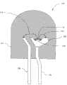
图1说明了这种类型的发光器件的截面结构。LED器件100设置有安装引线102及内部引线104。安装引线102还包括反射罩106,其中安装有蓝色发光二极管108。反射罩106填充有环氧树脂1 14,其中悬浮有粉末状磷光体。发光组件108的n电极及p电极通过接合线110及112分别连接至安装引线102及内部引线104。FIG. 1 illustrates the cross-sectional structure of this type of light emitting device. The
磷光体可以是Ce掺杂YAG,其制成为粉末形式并悬浮在用于密封管芯的环氧树脂114中。该磷光体环氧混合物填充反射罩106(其将管芯支撑在安装引线102上),且来自芯片的蓝色发光的一部分由磷光体吸收并以较长的磷光波长再次发出。因为仅需要一种类型的转换物,故在蓝光照射下组合黄色光激发是理想的。互补的蓝色及黄色波长通过迭加混合以产生所需的白色光。LED的合成发光光谱表现为磷光体发光与通过磷光体涂层的未被吸收的蓝色发光的组合。The phosphor may be Ce-doped YAG made in powder form and suspended in
白光二极管可根据另一机理而发光,即,利用由近紫色或紫外光辐射光学激发的宽光谱磷光体。在这种器件中,利用紫外发光二极管以向磷光体传送能量,而由磷光体产生全部可见发光。以这种方法产生白色光的优点在于其达到的彩色性能优于蓝色发光LED,这是因为UV LED对由该器件所产生的可见颜色不会有大的影响。White light emitting diodes may emit light according to another mechanism, namely, using broad-spectrum phosphors that are optically excited by near-violet or ultraviolet radiation. In such devices, UV LEDs are used to deliver energy to the phosphor, which produces all visible light emission. The advantage of producing white light in this way is that it achieves better color performance than blue-emitting LEDs because UV LEDs do not have a large effect on the visible color produced by the device.
很容易获得在较宽波长范围上发光并产生白色光的磷光体,这是因为相同的材料应用于制造荧光管及阴极射线管。尽管荧光管通过气体放电过程而实现其UV发光,但产生白色光输出的磷光体发光阶段与UV激发的白色二极管中的相同。磷光体具有公知的彩色特性,故这种类型的器件具有其可被设计用于需要关键性的颜色渲染的应用的优点。但是,相较于采用蓝色光进行荧光激发的白色二极管,UV激发二极管的很大的缺点在于其较差的发光效率。这是因为从UV光到更长的可见波长的降频转换中能量损耗较高。Phosphors that emit light over a broad range of wavelengths and produce white light are readily available because the same materials are used in the manufacture of fluorescent and cathode ray tubes. Although fluorescent tubes achieve their UV emission through a gas discharge process, the phase of phosphor emission that produces white light output is the same as in UV excited white diodes. Phosphors have well known color properties, so this type of device has the advantage that it can be designed for applications requiring critical color rendering. However, compared with white diodes that use blue light for fluorescence excitation, a great disadvantage of UV excitation diodes is their poor luminous efficiency. This is due to the higher energy loss in the down conversion from UV light to longer visible wavelengths.
此外,使用UV LED的另一个缺点在于,由于较高的光子能量会导致化学键断裂以及环氧材料的结构分解,封装材料(即,围绕二极管用于密封发光器件的环氧树脂)会快速劣化。这导致照明(“Lv”)劣化,即由于磷光体/环氧材料受到来自UV LED的UV照射,随着时间流逝,输出的光减少了。此外,使用UV发光也增加了对人眼的伤害的危险,而需要对其补偿。In addition, another disadvantage of using UV LEDs is that the encapsulation material (i.e., the epoxy that surrounds the diode to seal the light-emitting device) degrades rapidly due to the higher photon energy causing chemical bond breakage and structural breakdown of the epoxy material. This leads to illumination (“Lv”) degradation, i.e. a decrease in light output over time as the phosphor/epoxy material is exposed to UV radiation from the UV LED. Furthermore, the use of UV light also increases the risk of damage to the human eye, which needs to be compensated for.
因此,需要减小在UV LED中UV环氧树脂或UV材料劣化的影响,由此改善发光效率及光源的使用寿命。此外,因为需要保护人眼,需要防止UV发光从LED漏出。Therefore, there is a need to reduce the effect of UV epoxy resin or UV material degradation in UV LEDs, thereby improving the luminous efficiency and the service life of the light source. In addition, because of the need to protect human eyes, it is necessary to prevent UV light from leaking from the LED.
发明内容Contents of the invention
本发明揭示了一种光源,其可利用紫外(“UV”)发光二极管(“LED”)器件及UV反光板产生白色光。该光源可包括UV LED作为其辐射源,所述UV LED发出例如近紫色或紫外光的较短波长的光,还包括可以沉积或涂在UV LED的表面上的磷光体的薄膜。该光源还可包括设置在薄的磷光体层之上的UV反光板材料。The present invention discloses a light source that utilizes ultraviolet ("UV") light emitting diode ("LED") devices and UV reflectors to generate white light. The light source may include as its radiation source a UV LED emitting shorter wavelength light such as near violet or ultraviolet light, and a thin film of phosphor that may be deposited or coated on the surface of the UV LED. The light source may also include a UV reflective material disposed over the thin phosphor layer.
在工作的示例中,UV LED发出较短波长的光,接着该光照在薄的磷光体层上。部分较短波长的光被磷光体层转化为白色光,而较短波长的光的另一部分穿过磷光体层透射。穿过磷光体层的那部分光照在UV反光板上,所述UV反光板允许可见光穿过并将UV光反射回至磷光体层。磷光体层将反射的UV光转化为白色光,然后所述白色光通过磷光体层再次发出。In the working example, a UV LED emits light of a shorter wavelength, which then shines on a thin phosphor layer. Part of the shorter wavelength light is converted to white light by the phosphor layer, while another part of the shorter wavelength light is transmitted through the phosphor layer. The portion of the light that passes through the phosphor layer hits a UV reflective plate that allows visible light to pass through and reflects the UV light back to the phosphor layer. The phosphor layer converts the reflected UV light into white light, which is then re-emitted through the phosphor layer.
通过研究以下附图及详细说明,本领域的技术人员将明白本发明的其他系统、方法及特征。意在将所有这些其他系统、方法、特征及优点包括在该说明中、落入本发明的范围内、并由所附权利要求保护。Other systems, methods and features of the present invention will be apparent to those skilled in the art from a study of the following figures and detailed description. It is intended that all such other systems, methods, features and advantages be included within this description, be within the scope of the invention, and be protected by the following claims.
附图说明Description of drawings
参考以下附图可以更好的理解本发明。图中的组件并不一定完全成比例,重点在于说明本发明的原理。在附图中,类似的参考标号用于表示各个示图中相应的部件。The invention can be better understood with reference to the following figures. The components in the figures are not necessarily to scale, emphasis instead being placed upon illustrating the principles of the invention. In the drawings, like reference numerals are used to indicate corresponding parts in the various views.
图1示出了示意性截面图,说明了包括LED的已知光源的应用的示例。Fig. 1 shows a schematic cross-sectional view illustrating an example of application of a known light source comprising LEDs.
图2示出了示意性截面图,说明了包括UV LED及UV反光板的光源的应用的示例。Figure 2 shows a schematic cross-sectional view illustrating an example of an application of a light source comprising a UV LED and a UV reflector.
图3示出了图2中所示的光源的示意性截面图,更详细的说明了UVLED及UV反光板。Fig. 3 shows a schematic cross-sectional view of the light source shown in Fig. 2, illustrating the UV LED and the UV reflector in more detail.
图4示出了对于图2及图3中所示的UV反光板的示例应用,反射率随着以纳米(“nm”)为单位的光波长变化的图形表示。4 shows a graphical representation of reflectivity as a function of wavelength of light in nanometers ("nm") for an example application of the UV reflective sheeting shown in FIGS. 2 and 3 .
具体实施方式Detailed ways
在优选实施例的以下描述中,参考组成其一部分的附图,且其示意性的示出了可实施本发明的具体实施例。不脱离本发明的范围,也可以采用其他实施例并进行结构改变。In the following description of the preferred embodiments, reference is made to the accompanying drawings which form a part hereof, and which are schematic illustrations of specific embodiments in which the invention may be practiced. Other embodiments may be utilized and structural changes may be made without departing from the scope of the present invention.
大体上,本发明为一种光源,其可包括可以是紫外(“UV”)发光二极管(“LED”)的辐射源,该LED发出可以是在可见及不可见光光谱上的近紫色或紫外光的较短波长的光,即,具有约400纳米(“nm”)或更短的波长的光。大体上,术语“UV光”指具有不能被人眼所观察到的波长的光。In general, the present invention is a light source that may include a radiation source that may be an ultraviolet ("UV") light emitting diode ("LED") that emits near-violet or ultraviolet light that may be on the visible and invisible light spectrum Light having shorter wavelengths, ie, light having a wavelength of about 400 nanometers ("nm") or shorter. In general, the term "UV light" refers to light having wavelengths that cannot be observed by the human eye.
该光源还可以包括薄的磷光体层或涂附在UV LED的表面上的磷光体涂层。在薄的磷光体层上可以设置可反射由UV LED发出的UV光并允许较长波长的光通过其的UV反光板。被反射的UV光可再次射向薄的磷光体层,由此将反射的UV光转换为可见光,接着可见光穿过UV反光板,产生基于薄的磷光体层中的磷光体材料的色度(shade)的白色光。The light source may also include a thin phosphor layer or a phosphor coating applied to the surface of the UV LED. A UV reflector that reflects the UV light emitted by the UV LED and allows longer wavelength light to pass through it can be placed on the thin phosphor layer. The reflected UV light can be directed again towards the thin phosphor layer, thereby converting the reflected UV light to visible light, which then passes through the UV reflector, producing a chromaticity based on the phosphor material in the thin phosphor layer ( shade) of white light.
图2示出了可产生可见光的光源的应用示例的示意性截面图。光源200设置有安装引线202及内部引线204。安装引线202还包括反射罩206,其中附装有UV发光二极管208。UV发光二极管208的n电极及p电极(未示出)通过单独的接合线(未示出)分别连接至安装引线202及内部引线204。Fig. 2 shows a schematic cross-sectional view of an application example of a light source that can generate visible light. The
薄的磷光体层222可以直接涂在UV发光二极管208的表面上。薄的磷光体层222可以包含单一磷光体或多种磷光体的组合,当由来自UV发光二极管208的UV光激发时其将发出白色光。在另一应用中,磷光体可以悬浮在分布于UV发光二极管208的表面上的密封材料中。用于在半导体器件上沉积材料的方法,例如,在LED上沉积磷光体,在标题为“Electrophoretic Processes for the Selective Deposition of Materials on aSemiconducting Device”、于2005年3月8日公告的U.S.Patent No.6,864,110中进行了描述,在这里通过参考其全文而结合在本文中。A thin phosphor layer 222 can be coated directly on the surface of the UV light emitting diode 208 . Thin phosphor layer 222 may contain a single phosphor or a combination of phosphors that will emit white light when excited by UV light from UV light emitting diode 208 . In another application, the phosphor may be suspended in an encapsulant that is distributed over the surface of the UV light emitting diode 208 . Methods for depositing materials on semiconductor devices, e.g., phosphor deposits on LEDs, in U.S. Patent No. 1, published March 8, 2005, entitled "Electrophoretic Processes for the Selective Deposition of Materials on a Semiconductor Device" 6,864,110, which is hereby incorporated by reference in its entirety.
UV反光板224定位在薄的磷光体层222之上。在图2中示出UV反光板224直接附装在薄的磷光体层222上并大体为相同尺寸。但是,UV反光板也可以直接定位在薄的磷光体层222上并与其分离,并且可以是与薄的磷光体层222不同的尺寸,例如,UV反光板224可以更宽并叠置在薄的磷光体层222上。A UV reflective plate 224 is positioned over the thin phosphor layer 222 . In FIG. 2 the UV reflector 224 is shown attached directly on the thin phosphor layer 222 and is generally the same size. However, the UV reflector can also be positioned directly on and separated from the thin phosphor layer 222, and can be of a different size than the thin phosphor layer 222, for example, the UV reflector 224 can be wider and stacked on top of the thin phosphor layer 222. on the phosphor layer 222 .
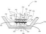
图3示出了图2中的光源的示意性截面图,其更详细的示出了UVLED及UV反光板。在图3中,UV发光二极管308由反射罩306支撑并发出具有例如从380nm至410nm的波长的UV光330。UV光330“激发”薄的磷光体层322,且一部分UV光330由薄的磷光体层322吸收并转化为较长波长的光332。较长波长的光332穿过UV反光板324并变为可见光334。Fig. 3 shows a schematic cross-sectional view of the light source in Fig. 2, which shows the UV LED and the UV reflector in more detail. In FIG. 3, a UV
UV光330的某些部分不会被薄的磷光体层322所转化,由此从薄的磷光体层322发出较短波长的光336。较短波长的光336被UV反光板324反射,产生反射光338。接着该反射光338“激发”薄的磷光体层322,产生另一较长波长的光340。该较长波长的光340穿过薄的磷光体层322,产生另一可见光342。Some portion of the
图4示出了对于图2及3中所示的UV反光板的示例应用,反射率随着以纳米(“nm”)为单位的光波长变化的图形表示。图4描述了理想的UV反光板,其基本上反射全部的具有约350nm或更短波长的光,同时允许具有约450nm或更长波长的光穿过。4 shows a graphical representation of reflectivity as a function of wavelength of light in nanometers ("nm") for an example application of the UV reflective sheeting shown in FIGS. 2 and 3. FIG. Figure 4 depicts an ideal UV reflective sheet that reflects substantially all light having a wavelength of about 350 nm or less while allowing light having a wavelength of about 450 nm or longer to pass through.
虽然以上的描述参考使用UV LED,但主题不应限于以这种器件作为辐射源。可受益于由上述组件提供的功能的任何半导体辐射源都可以应用为光源,包括半导体激光二极管。Although the above description refers to the use of UV LEDs, the subject matter should not be limited to using such devices as radiation sources. Any semiconductor radiation source that would benefit from the functionality provided by the components described above may be employed as a light source, including semiconductor laser diodes.
此外,需要理解的是,上述多种应用的描述目的仅在于说明而非限制。并不是绝对的且不应将所请求保护的发明限制为所揭示的特定形式。鉴于以上描述,修改及改变是可行的,或可以通过实践本发明而获得。权利要求及其等同物界定了本发明的范围。In addition, it should be understood that the above descriptions of various applications are for illustration purposes only and not for limitation. It is not intended to be absolute and should not limit the claimed invention to the particular forms disclosed. In light of the foregoing description, modifications and alterations are possible or may be acquired by practice of the invention. The claims and their equivalents define the scope of the invention.
Claims (20)
Translated fromChineseApplications Claiming Priority (2)
| Application Number | Priority Date | Filing Date | Title |
|---|---|---|---|
| US11/210,714US20070045641A1 (en) | 2005-08-23 | 2005-08-23 | Light source with UV LED and UV reflector |
| US11/210,714 | 2005-08-23 |
Publications (2)
| Publication Number | Publication Date |
|---|---|
| CN1921159A CN1921159A (en) | 2007-02-28 |
| CN1921159Btrue CN1921159B (en) | 2012-01-18 |
Family
ID=37102665
Family Applications (1)
| Application Number | Title | Priority Date | Filing Date |
|---|---|---|---|
| CN2006101114626AExpired - Fee RelatedCN1921159B (en) | 2005-08-23 | 2006-08-22 | Light source with UV LED and UV reflector |
Country Status (5)
| Country | Link |
|---|---|
| US (1) | US20070045641A1 (en) |
| JP (1) | JP2007059911A (en) |
| CN (1) | CN1921159B (en) |
| GB (1) | GB2430305A (en) |
| TW (1) | TW200715620A (en) |
Families Citing this family (42)
| Publication number | Priority date | Publication date | Assignee | Title |
|---|---|---|---|---|
| US9412926B2 (en) | 2005-06-10 | 2016-08-09 | Cree, Inc. | High power solid-state lamp |
| US7703945B2 (en)* | 2006-06-27 | 2010-04-27 | Cree, Inc. | Efficient emitting LED package and method for efficiently emitting light |
| JP2010527510A (en)* | 2007-05-08 | 2010-08-12 | クリー エル イー ディー ライティング ソリューションズ インコーポレイテッド | Lighting device and lighting method |
| KR100888438B1 (en)* | 2007-11-22 | 2009-03-11 | 삼성전기주식회사 | White light emitting device and its manufacturing method |
| US8058088B2 (en)* | 2008-01-15 | 2011-11-15 | Cree, Inc. | Phosphor coating systems and methods for light emitting structures and packaged light emitting diodes including phosphor coating |
| US8940561B2 (en)* | 2008-01-15 | 2015-01-27 | Cree, Inc. | Systems and methods for application of optical materials to optical elements |
| CN102196759B (en) | 2008-10-27 | 2014-05-28 | 奥林巴斯医疗株式会社 | Body-introduced device and medical system |
| KR101577300B1 (en)* | 2008-10-28 | 2015-12-15 | 삼성디스플레이 주식회사 | Light Emitting Diode Using Quantum Dot And Backlight Assembly Having The Same |
| US8562161B2 (en) | 2010-03-03 | 2013-10-22 | Cree, Inc. | LED based pedestal-type lighting structure |
| US9500325B2 (en) | 2010-03-03 | 2016-11-22 | Cree, Inc. | LED lamp incorporating remote phosphor with heat dissipation features |
| US9316361B2 (en) | 2010-03-03 | 2016-04-19 | Cree, Inc. | LED lamp with remote phosphor and diffuser configuration |
| US9057511B2 (en) | 2010-03-03 | 2015-06-16 | Cree, Inc. | High efficiency solid state lamp and bulb |
| US10359151B2 (en) | 2010-03-03 | 2019-07-23 | Ideal Industries Lighting Llc | Solid state lamp with thermal spreading elements and light directing optics |
| US9062830B2 (en) | 2010-03-03 | 2015-06-23 | Cree, Inc. | High efficiency solid state lamp and bulb |
| US9625105B2 (en) | 2010-03-03 | 2017-04-18 | Cree, Inc. | LED lamp with active cooling element |
| US8931933B2 (en) | 2010-03-03 | 2015-01-13 | Cree, Inc. | LED lamp with active cooling element |
| US8632196B2 (en) | 2010-03-03 | 2014-01-21 | Cree, Inc. | LED lamp incorporating remote phosphor and diffuser with heat dissipation features |
| US9310030B2 (en) | 2010-03-03 | 2016-04-12 | Cree, Inc. | Non-uniform diffuser to scatter light into uniform emission pattern |
| US9024517B2 (en) | 2010-03-03 | 2015-05-05 | Cree, Inc. | LED lamp with remote phosphor and diffuser configuration utilizing red emitters |
| US20110220920A1 (en)* | 2010-03-09 | 2011-09-15 | Brian Thomas Collins | Methods of forming warm white light emitting devices having high color rendering index values and related light emitting devices |
| US10451251B2 (en) | 2010-08-02 | 2019-10-22 | Ideal Industries Lighting, LLC | Solid state lamp with light directing optics and diffuser |
| CN102623607A (en)* | 2011-01-28 | 2012-08-01 | 联胜(中国)科技有限公司 | Luminescent module |
| US9166126B2 (en) | 2011-01-31 | 2015-10-20 | Cree, Inc. | Conformally coated light emitting devices and methods for providing the same |
| US9508904B2 (en) | 2011-01-31 | 2016-11-29 | Cree, Inc. | Structures and substrates for mounting optical elements and methods and devices for providing the same background |
| US9068701B2 (en) | 2012-01-26 | 2015-06-30 | Cree, Inc. | Lamp structure with remote LED light source |
| US9234655B2 (en) | 2011-02-07 | 2016-01-12 | Cree, Inc. | Lamp with remote LED light source and heat dissipating elements |
| US11251164B2 (en) | 2011-02-16 | 2022-02-15 | Creeled, Inc. | Multi-layer conversion material for down conversion in solid state lighting |
| TWI435481B (en)* | 2011-02-18 | 2014-04-21 | Genesis Photonics Inc | Light emitting diode device |
| US9488359B2 (en) | 2012-03-26 | 2016-11-08 | Cree, Inc. | Passive phase change radiators for LED lamps and fixtures |
| TW201517316A (en)* | 2013-10-22 | 2015-05-01 | Lextar Electronics Corp | Light-emitting diode package structure and light-emitting diode package module |
| US9360188B2 (en) | 2014-02-20 | 2016-06-07 | Cree, Inc. | Remote phosphor element filled with transparent material and method for forming multisection optical elements |
| JP6179628B2 (en)* | 2016-03-23 | 2017-08-16 | セイコーエプソン株式会社 | LIGHTING DEVICE, ELECTRONIC DEVICE, AND PROJECTION TYPE DISPLAY DEVICE |
| US20190377538A1 (en) | 2018-06-08 | 2019-12-12 | Curious Company, LLC | Information Presentation Through Ambient Sounds |
| US10650600B2 (en) | 2018-07-10 | 2020-05-12 | Curious Company, LLC | Virtual path display |
| US10818088B2 (en) | 2018-07-10 | 2020-10-27 | Curious Company, LLC | Virtual barrier objects |
| US10902678B2 (en) | 2018-09-06 | 2021-01-26 | Curious Company, LLC | Display of hidden information |
| US11055913B2 (en) | 2018-12-04 | 2021-07-06 | Curious Company, LLC | Directional instructions in an hybrid reality system |
| US10970935B2 (en) | 2018-12-21 | 2021-04-06 | Curious Company, LLC | Body pose message system |
| US10872584B2 (en)* | 2019-03-14 | 2020-12-22 | Curious Company, LLC | Providing positional information using beacon devices |
| US11786622B2 (en) | 2020-05-08 | 2023-10-17 | Ultra-Violet Solutions, Llc | Far UV-C light apparatus |
| US12106956B2 (en) | 2021-05-18 | 2024-10-01 | B/E Aerospace, Inc. | Color mixed excimer lamp for soft glow effect |
| DE202023106577U1 (en) | 2023-11-10 | 2024-01-29 | Jk-Holding Gmbh | Illumination device emitting light in the UV and VIS range |
Citations (1)
| Publication number | Priority date | Publication date | Assignee | Title |
|---|---|---|---|---|
| US6653765B1 (en)* | 2000-04-17 | 2003-11-25 | General Electric Company | Uniform angular light distribution from LEDs |
Family Cites Families (13)
| Publication number | Priority date | Publication date | Assignee | Title |
|---|---|---|---|---|
| TW383508B (en)* | 1996-07-29 | 2000-03-01 | Nichia Kagaku Kogyo Kk | Light emitting device and display |
| US5813752A (en)* | 1997-05-27 | 1998-09-29 | Philips Electronics North America Corporation | UV/blue LED-phosphor device with short wave pass, long wave pass band pass and peroit filters |
| US5962971A (en)* | 1997-08-29 | 1999-10-05 | Chen; Hsing | LED structure with ultraviolet-light emission chip and multilayered resins to generate various colored lights |
| US6340824B1 (en)* | 1997-09-01 | 2002-01-22 | Kabushiki Kaisha Toshiba | Semiconductor light emitting device including a fluorescent material |
| US6635363B1 (en)* | 2000-08-21 | 2003-10-21 | General Electric Company | Phosphor coating with self-adjusting distance from LED chip |
| US20020084748A1 (en)* | 2000-12-28 | 2002-07-04 | Ayala Raul E. | UV Reflecting materials for LED lamps using UV-emitting diodes |
| US6686676B2 (en)* | 2001-04-30 | 2004-02-03 | General Electric Company | UV reflectors and UV-based light sources having reduced UV radiation leakage incorporating the same |
| US20050040410A1 (en)* | 2002-02-12 | 2005-02-24 | Nl-Nanosemiconductor Gmbh | Tilted cavity semiconductor optoelectronic device and method of making same |
| US6864110B2 (en)* | 2002-10-22 | 2005-03-08 | Agilent Technologies, Inc. | Electrophoretic processes for the selective deposition of materials on a semiconducting device |
| US6765237B1 (en)* | 2003-01-15 | 2004-07-20 | Gelcore, Llc | White light emitting device based on UV LED and phosphor blend |
| US20040145312A1 (en)* | 2003-01-27 | 2004-07-29 | 3M Innovative Properties Company | Phosphor based light source having a flexible short pass reflector |
| US7204631B2 (en)* | 2004-06-30 | 2007-04-17 | 3M Innovative Properties Company | Phosphor based illumination system having a plurality of light guides and an interference reflector |
| TWI239671B (en)* | 2004-12-30 | 2005-09-11 | Ind Tech Res Inst | LED applied with omnidirectional reflector |
- 2005
- 2005-08-23USUS11/210,714patent/US20070045641A1/ennot_activeAbandoned
- 2006
- 2006-08-18TWTW095130408Apatent/TW200715620A/enunknown
- 2006-08-22GBGB0616653Apatent/GB2430305A/ennot_activeWithdrawn
- 2006-08-22CNCN2006101114626Apatent/CN1921159B/ennot_activeExpired - Fee Related
- 2006-08-23JPJP2006226303Apatent/JP2007059911A/enactivePending
Patent Citations (1)
| Publication number | Priority date | Publication date | Assignee | Title |
|---|---|---|---|---|
| US6653765B1 (en)* | 2000-04-17 | 2003-11-25 | General Electric Company | Uniform angular light distribution from LEDs |
Also Published As
| Publication number | Publication date |
|---|---|
| US20070045641A1 (en) | 2007-03-01 |
| TW200715620A (en) | 2007-04-16 |
| CN1921159A (en) | 2007-02-28 |
| JP2007059911A (en) | 2007-03-08 |
| GB0616653D0 (en) | 2006-10-04 |
| GB2430305A (en) | 2007-03-21 |
Similar Documents
| Publication | Publication Date | Title |
|---|---|---|
| CN1921159B (en) | Light source with UV LED and UV reflector | |
| JP5951180B2 (en) | Emitter package with saturation conversion material | |
| US6747406B1 (en) | LED cross-linkable phospor coating | |
| US6603258B1 (en) | Light emitting diode device that emits white light | |
| JP5519552B2 (en) | Phosphor material | |
| KR102184381B1 (en) | Light emitting device having uv light diode and lighting apparatus including the same | |
| CN100557833C (en) | Light-emitting semiconductor device and device including the light-emitting semiconductor device | |
| CN108305929B (en) | White light-emitting device with high color rendering | |
| KR101265094B1 (en) | White light emitting diode and method for producing the same | |
| US12369438B2 (en) | System and method for providing color light sources in proximity to predetermined wavelength conversion structures | |
| EP1528604A2 (en) | Semiconductor light emitting devices with enhanced luminous efficiency | |
| CN101184823A (en) | Lighting system comprising luminescent material compensating for color defects | |
| CN102804423A (en) | Phosphor converting IR LEDs | |
| JP2010034183A (en) | Light-emitting device | |
| JP2016523443A (en) | Solid light emitter package, light emitting device, flexible LED strip, and luminaire | |
| CN103779373A (en) | Light-emitting device and method of manufacturing the same | |
| CN102544326B (en) | Fluorescent substance with Ce3+ /Ce3+, Li+ doped luminescent material | |
| JP4857735B2 (en) | Light emitting device | |
| JP2005332951A (en) | Light emitting device | |
| CN101353572B (en) | Wavelength conversion system | |
| JP4591106B2 (en) | White light emitting device | |
| JP2004103814A (en) | Light emitting diode, its manufacturing method and white light illumination device | |
| CN103972366A (en) | Wavelength conversion substance, wavelength conversion colloid and light-emitting device | |
| KR100684043B1 (en) | White light emitting diode and its manufacturing method | |
| JP2008227550A (en) | Light emitting diode, its production method, and white lighting apparatus |
Legal Events
| Date | Code | Title | Description |
|---|---|---|---|
| C06 | Publication | ||
| PB01 | Publication | ||
| C10 | Entry into substantive examination | ||
| SE01 | Entry into force of request for substantive examination | ||
| C14 | Grant of patent or utility model | ||
| GR01 | Patent grant | ||
| C17 | Cessation of patent right | ||
| CF01 | Termination of patent right due to non-payment of annual fee | Granted publication date:20120118 Termination date:20130822 |