CN1914351A - Selectable dual position magnetron - Google Patents
Selectable dual position magnetronDownload PDFInfo
- Publication number
- CN1914351A CN1914351ACNA2005800038296ACN200580003829ACN1914351ACN 1914351 ACN1914351 ACN 1914351ACN A2005800038296 ACNA2005800038296 ACN A2005800038296ACN 200580003829 ACN200580003829 ACN 200580003829ACN 1914351 ACN1914351 ACN 1914351A
- Authority
- CN
- China
- Prior art keywords
- magnetron
- pivot
- central shaft
- around
- target
- Prior art date
- Legal status (The legal status is an assumption and is not a legal conclusion. Google has not performed a legal analysis and makes no representation as to the accuracy of the status listed.)
- Granted
Links
- 230000009977dual effectEffects0.000titleclaimsdescription4
- 230000004888barrier functionEffects0.000claimsabstractdescription38
- 239000000463materialSubstances0.000claimsabstractdescription27
- 230000007246mechanismEffects0.000claimsabstractdescription26
- 238000005477sputtering targetMethods0.000claimsabstractdescription6
- 230000005291magnetic effectEffects0.000claimsdescription34
- 238000000034methodMethods0.000claimsdescription28
- 229910052751metalInorganic materials0.000claimsdescription17
- 239000002184metalSubstances0.000claimsdescription17
- 238000000151depositionMethods0.000claimsdescription12
- IJGRMHOSHXDMSA-UHFFFAOYSA-NAtomic nitrogenChemical compoundN#NIJGRMHOSHXDMSA-UHFFFAOYSA-N0.000claimsdescription11
- 230000008021depositionEffects0.000claimsdescription9
- 239000012530fluidSubstances0.000claimsdescription8
- 239000007788liquidSubstances0.000claimsdescription6
- 229910052757nitrogenInorganic materials0.000claimsdescription5
- 230000008859changeEffects0.000claimsdescription3
- 238000001816coolingMethods0.000claimsdescription3
- 239000013077target materialSubstances0.000claimsdescription3
- NJPPVKZQTLUDBO-UHFFFAOYSA-NnovaluronChemical compoundC1=C(Cl)C(OC(F)(F)C(OC(F)(F)F)F)=CC=C1NC(=O)NC(=O)C1=C(F)C=CC=C1FNJPPVKZQTLUDBO-UHFFFAOYSA-N0.000claims5
- 238000002294plasma sputter depositionMethods0.000claims5
- 208000005168IntussusceptionDiseases0.000claims2
- 230000008485antagonismEffects0.000claims2
- 238000001755magnetron sputter depositionMethods0.000claims2
- 230000009970fire resistant effectEffects0.000claims1
- 230000014759maintenance of locationEffects0.000claims1
- 238000004544sputter depositionMethods0.000abstractdescription60
- 230000033001locomotionEffects0.000abstractdescription25
- 238000004140cleaningMethods0.000abstractdescription20
- 235000012431wafersNutrition0.000description25
- 210000002381plasmaAnatomy0.000description18
- XKRFYHLGVUSROY-UHFFFAOYSA-NArgonChemical compound[Ar]XKRFYHLGVUSROY-UHFFFAOYSA-N0.000description15
- 229910052802copperInorganic materials0.000description15
- 239000010949copperSubstances0.000description15
- RYGMFSIKBFXOCR-UHFFFAOYSA-NCopperChemical compound[Cu]RYGMFSIKBFXOCR-UHFFFAOYSA-N0.000description14
- 230000008569processEffects0.000description11
- 229910052786argonInorganic materials0.000description8
- 239000007789gasSubstances0.000description8
- 150000002500ionsChemical class0.000description8
- 150000004767nitridesChemical class0.000description6
- 230000035939shockEffects0.000description6
- 239000004677NylonSubstances0.000description5
- 239000000498cooling waterSubstances0.000description5
- 230000003628erosive effectEffects0.000description5
- 150000002739metalsChemical class0.000description5
- 229920001778nylonPolymers0.000description5
- 238000005240physical vapour depositionMethods0.000description5
- PXHVJJICTQNCMI-UHFFFAOYSA-NNickelChemical compound[Ni]PXHVJJICTQNCMI-UHFFFAOYSA-N0.000description4
- 229910052782aluminiumInorganic materials0.000description4
- XAGFODPZIPBFFR-UHFFFAOYSA-NaluminiumChemical compound[Al]XAGFODPZIPBFFR-UHFFFAOYSA-N0.000description4
- 238000010586diagramMethods0.000description4
- 230000005484gravityEffects0.000description4
- 238000005546reactive sputteringMethods0.000description4
- 239000006096absorbing agentSubstances0.000description3
- 230000004907fluxEffects0.000description3
- 239000002245particleSubstances0.000description3
- 238000007747platingMethods0.000description3
- 239000000758substrateSubstances0.000description3
- 229910052715tantalumInorganic materials0.000description3
- GUVRBAGPIYLISA-UHFFFAOYSA-Ntantalum atomChemical compound[Ta]GUVRBAGPIYLISA-UHFFFAOYSA-N0.000description3
- ZOKXTWBITQBERF-UHFFFAOYSA-NMolybdenumChemical compound[Mo]ZOKXTWBITQBERF-UHFFFAOYSA-N0.000description2
- ATJFFYVFTNAWJD-UHFFFAOYSA-NTinChemical compound[Sn]ATJFFYVFTNAWJD-UHFFFAOYSA-N0.000description2
- RTAQQCXQSZGOHL-UHFFFAOYSA-NTitaniumChemical compound[Ti]RTAQQCXQSZGOHL-UHFFFAOYSA-N0.000description2
- 239000010941cobaltSubstances0.000description2
- 229910017052cobaltInorganic materials0.000description2
- GUTLYIVDDKVIGB-UHFFFAOYSA-Ncobalt atomChemical compound[Co]GUTLYIVDDKVIGB-UHFFFAOYSA-N0.000description2
- 230000008878couplingEffects0.000description2
- 238000010168coupling processMethods0.000description2
- 238000005859coupling reactionMethods0.000description2
- 230000000694effectsEffects0.000description2
- 239000003302ferromagnetic materialSubstances0.000description2
- 229910001092metal group alloyInorganic materials0.000description2
- 238000001465metallisationMethods0.000description2
- 239000011733molybdenumSubstances0.000description2
- 229910052750molybdenumInorganic materials0.000description2
- 229910052759nickelInorganic materials0.000description2
- 238000001552radio frequency sputter depositionMethods0.000description2
- 239000010936titaniumSubstances0.000description2
- 229910052719titaniumInorganic materials0.000description2
- 230000007704transitionEffects0.000description2
- 238000009825accumulationMethods0.000description1
- 238000005275alloyingMethods0.000description1
- 238000013459approachMethods0.000description1
- -1argon ionsChemical class0.000description1
- QVGXLLKOCUKJST-UHFFFAOYSA-Natomic oxygenChemical compound[O]QVGXLLKOCUKJST-UHFFFAOYSA-N0.000description1
- WYEMLYFITZORAB-UHFFFAOYSA-NboscalidChemical compoundC1=CC(Cl)=CC=C1C1=CC=CC=C1NC(=O)C1=CC=CN=C1ClWYEMLYFITZORAB-UHFFFAOYSA-N0.000description1
- 239000000872bufferSubstances0.000description1
- 239000000919ceramicSubstances0.000description1
- 230000006835compressionEffects0.000description1
- 238000007906compressionMethods0.000description1
- 239000000110cooling liquidSubstances0.000description1
- 239000008367deionised waterSubstances0.000description1
- 229910021641deionized waterInorganic materials0.000description1
- 229910001873dinitrogenInorganic materials0.000description1
- 238000006073displacement reactionMethods0.000description1
- 230000002349favourable effectEffects0.000description1
- 239000012634fragmentSubstances0.000description1
- 230000003116impacting effectEffects0.000description1
- 238000011065in-situ storageMethods0.000description1
- 230000006698inductionEffects0.000description1
- 239000012212insulatorSubstances0.000description1
- 238000002955isolationMethods0.000description1
- 239000006148magnetic separatorSubstances0.000description1
- 230000005389magnetismEffects0.000description1
- 238000004519manufacturing processMethods0.000description1
- 239000003550markerSubstances0.000description1
- 229910001172neodymium magnetInorganic materials0.000description1
- 230000007935neutral effectEffects0.000description1
- TWNQGVIAIRXVLR-UHFFFAOYSA-Noxo(oxoalumanyloxy)alumaneChemical compoundO=[Al]O[Al]=OTWNQGVIAIRXVLR-UHFFFAOYSA-N0.000description1
- 239000001301oxygenSubstances0.000description1
- 229910052760oxygenInorganic materials0.000description1
- 230000035515penetrationEffects0.000description1
- 230000036316preloadEffects0.000description1
- 230000009467reductionEffects0.000description1
- 238000006798ring closing metathesis reactionMethods0.000description1
- 229910021332silicideInorganic materials0.000description1
- 125000006850spacer groupChemical group0.000description1
- 238000004901spallingMethods0.000description1
- 238000000992sputter etchingMethods0.000description1
- 239000010935stainless steelSubstances0.000description1
- 229910001220stainless steelInorganic materials0.000description1
- 230000003068static effectEffects0.000description1
- 230000002459sustained effectEffects0.000description1
- WFKWXMTUELFFGS-UHFFFAOYSA-NtungstenChemical compound[W]WFKWXMTUELFFGS-UHFFFAOYSA-N0.000description1
- 229910052721tungstenInorganic materials0.000description1
- 239000010937tungstenSubstances0.000description1
- XLYOFNOQVPJJNP-UHFFFAOYSA-NwaterChemical compoundOXLYOFNOQVPJJNP-UHFFFAOYSA-N0.000description1
Images


Classifications
- H—ELECTRICITY
- H01—ELECTRIC ELEMENTS
- H01J—ELECTRIC DISCHARGE TUBES OR DISCHARGE LAMPS
- H01J37/00—Discharge tubes with provision for introducing objects or material to be exposed to the discharge, e.g. for the purpose of examination or processing thereof
- H01J37/32—Gas-filled discharge tubes
- H01J37/34—Gas-filled discharge tubes operating with cathodic sputtering
- H01J37/3411—Constructional aspects of the reactor
- H01J37/345—Magnet arrangements in particular for cathodic sputtering apparatus
- H01J37/3455—Movable magnets
- C—CHEMISTRY; METALLURGY
- C23—COATING METALLIC MATERIAL; COATING MATERIAL WITH METALLIC MATERIAL; CHEMICAL SURFACE TREATMENT; DIFFUSION TREATMENT OF METALLIC MATERIAL; COATING BY VACUUM EVAPORATION, BY SPUTTERING, BY ION IMPLANTATION OR BY CHEMICAL VAPOUR DEPOSITION, IN GENERAL; INHIBITING CORROSION OF METALLIC MATERIAL OR INCRUSTATION IN GENERAL
- C23C—COATING METALLIC MATERIAL; COATING MATERIAL WITH METALLIC MATERIAL; SURFACE TREATMENT OF METALLIC MATERIAL BY DIFFUSION INTO THE SURFACE, BY CHEMICAL CONVERSION OR SUBSTITUTION; COATING BY VACUUM EVAPORATION, BY SPUTTERING, BY ION IMPLANTATION OR BY CHEMICAL VAPOUR DEPOSITION, IN GENERAL
- C23C14/00—Coating by vacuum evaporation, by sputtering or by ion implantation of the coating forming material
- C23C14/22—Coating by vacuum evaporation, by sputtering or by ion implantation of the coating forming material characterised by the process of coating
- C23C14/34—Sputtering
- C23C14/35—Sputtering by application of a magnetic field, e.g. magnetron sputtering
- H—ELECTRICITY
- H01—ELECTRIC ELEMENTS
- H01J—ELECTRIC DISCHARGE TUBES OR DISCHARGE LAMPS
- H01J37/00—Discharge tubes with provision for introducing objects or material to be exposed to the discharge, e.g. for the purpose of examination or processing thereof
- H01J37/32—Gas-filled discharge tubes
- H01J37/34—Gas-filled discharge tubes operating with cathodic sputtering
- H01J37/3402—Gas-filled discharge tubes operating with cathodic sputtering using supplementary magnetic fields
- H01J37/3405—Magnetron sputtering
- H01J37/3408—Planar magnetron sputtering
Landscapes
- Chemical & Material Sciences (AREA)
- Engineering & Computer Science (AREA)
- Physics & Mathematics (AREA)
- Plasma & Fusion (AREA)
- Analytical Chemistry (AREA)
- Chemical Kinetics & Catalysis (AREA)
- Materials Engineering (AREA)
- Mechanical Engineering (AREA)
- Metallurgy (AREA)
- Organic Chemistry (AREA)
- Physical Vapour Deposition (AREA)
- Electrodes Of Semiconductors (AREA)
Abstract
Translated fromChinese
Description
Translated fromChinese技术领域technical field
本发明通常涉及材料的溅射。尤其是,本发明涉及与磁控管形成磁场以增强溅射。The present invention generally relates to sputtering of materials. In particular, the invention relates to forming a magnetic field with a magnetron to enhance sputtering.
背景技术Background technique
溅射(sputtering)或称物理气相沉积(Physical Vapor Deposition,PVD)者是集成电路制造中沉积金属层及相关材料最常见的方法。溅射原先是用于在晶片上沉积相当平坦的材料层,且特别是用于沉积铝电内连线。然而近年来,焦点及挑战皆在于将材料沉积在高深宽比介电层中之垂直内连线,以及介电层中(及通过介电层)之类似垂直向结构中。铜金属化则因大块铜可更轻易通过电化学电镀(Electrochemical plating,ECP)沉积而改变了重要性。然而,在电化学电镀之前会需要各种薄衬层,例如阻挡层(如Ta及TaN)以避免铜扩散至氧化物介电层及铜晶种层,以形成平板电极并进行铜电化学电镀层的成长。Sputtering or physical vapor deposition (Physical Vapor Deposition, PVD) is the most common method for depositing metal layers and related materials in integrated circuit manufacturing. Sputtering was originally used to deposit relatively flat layers of material on wafers, and in particular to deposit aluminum electrical interconnects. In recent years, however, the focus and challenge has been on depositing materials in vertical interconnects in high aspect ratio dielectric layers, and similar vertically oriented structures in (and through) dielectric layers. Copper metallization has changed in importance as bulk copper can be more easily deposited by electrochemical plating (ECP). However, various thin liners such as barrier layers (such as Ta and TaN) are required before electrochemical plating to prevent copper from diffusing into the oxide dielectric layer and copper seed layer to form plate electrodes and perform copper electrochemical plating layer growth.
现已发展出许多技术可让薄均匀层溅射沉积在高深宽比孔的壁上。此种商业上已成功的技术之一为自离子化等离子(Self-Ionizing Plasma,SIP)溅射,其中多数溅射原子会离子化并因而可静电吸附于窄开孔内。称为自离子化等离子是因为部分溅射离子会被吸回至溅射靶材,以溅射出更多原子或离子,从而降低氩工作气体的需求并可于低压下进行溅射。SIP的极限是持续自溅射(SustainedSelf-Sputtering,SSS),其中溅射离子足以维持溅射等离子,因此去除氩气。A number of techniques have been developed to sputter-deposit thin uniform layers on the walls of high aspect ratio holes. One such commercially successful technique is Self-Ionizing Plasma (SIP) sputtering, where most of the sputtered atoms are ionized and thus electrostatically adsorbed within narrow openings. It is called self-ionizing plasma because some of the sputtered ions are attracted back to the sputtering target to sputter out more atoms or ions, thus reducing the requirement of argon working gas and allowing sputtering at low pressure. The limit of SIP is Sustained Self-Sputtering (SSS), where the sputtering ions are sufficient to maintain the sputtering plasma, thus removing argon.
公知的PVD腔室10(对于SSS或SIP溅射稍微有些变化)示意性地示出在图1中。该示意图是以加州圣塔克拉拉市美商应用材料公司所上市的EnduraPVD反应器为基础。该腔室10包括一真空腔室本体12,其经由一陶瓷绝缘体14与一溅射靶材16相封隔,该靶材16具有至少一正面,该正面由欲溅射沉积在一晶片18(通过一晶片夹钳承载于一加热器基座20上)上的材料所组成,其通常为金属。除了晶片夹钳22,覆盖环或静电吸盘也可结合至基座20,或该晶片也可置于基座20上而无需适当承载。靶材材料可为铝、铜、钛、钽、钴、镍、钼、这些金属的含有少于10wt%合金元素的金属合金,或其它金属以及耐受DC溅射的金属合金。另一方面,RF溅射也可用于溅射来自介电质靶材之材料。设于腔室本体12内的接地档板24可保护腔室壁12不受溅射材料的影响,并作为一接地阳极。一可选择及控制之DC电源供应器26可相对于档板24将靶材14负电地偏压至约-600伏特DC。通常,基座20以及晶片18是维持电浮动的方式,但对于多数类型的SIP溅射而言,RF电源供应器28经由AC电容耦合电路30或更复杂的匹配及绝缘电路耦接至基座18,以使基座电极20在等离子存在下可形成DC自偏压电压。负DC自偏压可将高密度等离子中的正电荷溅射离子吸引至高级集成电路的高深宽比孔的深处。即使在基座20是电浮动,其亦可形成部分DC自偏压。A known PVD chamber 10 (slightly modified for SSS or SIP sputtering) is shown schematically in FIG. 1 . The schematic is based on the Endura PVD reactor marketed by Applied Materials, Inc., Santa Clara, California. The
第一气体源34可经由质流控制器36将溅射工作气体(一般为氩气)供应至腔室本体12。在反应性金属氮化物(例如,氮化钛或氮化钽)溅射中,氮气是由另一气体源38经由其本身的质流控制器40进行供应。也可供应氧气以形成氧化物,如三氧化二铝。该气体可由该腔室本体12内不同位置进入。例如,位于靠近腔室本体12底部的一个或多个进气管可于档板24后方供应气体。气体会穿过该档板24底部的一孔径或通过在该覆盖环22与该档板24及该基座20间形成的一间隙24。经由一宽的抽吸口46连接至腔室本体12的真空抽吸系统44可将腔室本体12内部维持在低压。虽然基础压力可维持在约10-7托或甚至更低,但氩工作气体的通常压力通常是维持在约1至100毫托之间。然而对自离子溅射而言,压力可略小,例如低至0.1毫托。对持续自溅射而言,特别是溅射铜时,一旦等离子激发后,氩气的供应便可终止,且腔室压力可降至非常低。一基于计算机的控制器48包括DC电源供应器26及质流控制器36,40。The first gas source 34 can supply a sputtering working gas (typically argon) to the chamber body 12 via a mass flow controller 36 . In reactive metal nitride (eg TiN or TaN) sputtering, nitrogen gas is supplied from another gas source 38 via its own mass flow controller 40 . Oxygen may also be supplied to form oxides such as aluminum oxide. The gas can enter from different positions in the chamber body 12 . For example, one or more inlet ducts located near the bottom of the chamber body 12 may supply gas behind the baffle 24 . Gas passes through an aperture in the bottom of the baffle 24 or through a gap 24 formed between the cover ring 22 and the baffle 24 and the base 20 . A vacuum suction system 44 connected to the chamber body 12 via a wide suction port 46 maintains the interior of the chamber body 12 at a low pressure. Typical pressures for the argon working gas are typically maintained between about 1 and 100 mTorr, although the base pressure can be maintained at about 10-7 Torr or even lower. For self-ion sputtering, however, the pressure may be somewhat lower, for example as low as 0.1 mTorr. For continuous self-sputtering, especially copper sputtering, once the plasma is ignited, the argon supply can be terminated and the chamber pressure can be reduced to very low levels. A computer-based controller 48 includes the DC power supply 26 and the mass flow controllers 36,40.
当氩气进入腔室时,靶材16及挡板24间的DC电压会使氩气成为等离子,且带正电荷的氩离子会吸附至负电偏压的靶材16。该离子会以相当大的能量撞击靶材16,并使靶材粒子由靶材16溅射出。若干靶材粒子会撞击晶片18并因而沉积于其上,由此形成一靶材材料薄层。在反应性溅射金属氮化物中,氮会同时进入腔室本体12,并与溅射金属原子反应而在晶片18上形成金属氮化物。When argon enters the chamber, the DC voltage between the target 16 and the baffle 24 causes the argon to become a plasma, and the positively charged argon ions are attracted to the negatively biased target 16 . The ions will strike the target 16 with considerable energy and cause target particles to be sputtered from the target 16 . A number of target particles will strike the wafer 18 and thus deposit thereon, thereby forming a thin layer of target material. In reactive sputtering metal nitride nitrogen will simultaneously enter the chamber body 12 and react with the sputtered metal atoms to form metal nitride on the wafer 18 .
为提供有效的溅射,磁控管50会置于靶材16后方。其包括相对的磁铁52,54,以一磁性轭(magnetic yoke)56耦接以在腔室内该磁铁52,54附近形成磁场。一般而言在SIP溅射中,磁控管50很小、套叠且具一或多个内磁铁52(磁力相对更大的外磁铁54所环绕)而不平衡。磁场会捕捉电子,且对电荷中性区而言,离子密度也会增加以在腔室内该磁控管50附近形成高密度等离子区58。为了能在晶片18上进行均匀溅射,磁控管50通常会通过马达64驱动的一轴杆62绕着靶材16中心60旋转。一般转速为50至100rpm。在公知的磁控管中,轴杆62相对于磁控管52,54固定且与靶材中心60一致,以使磁控管50掠过靶材中心60周围的一固定路径。To provide efficient sputtering, a
Fu在美国专利第6,306,265号中公开了数种用于SSS及SIP的磁控管设计。对此等应用而言,磁控管应可产生强磁场且具有小面积。旋转磁控管仍可提供均匀溅射沉积以及最大靶材侵蚀(若需要)。磁控管应包括与一个或多个内磁铁52相连的一内磁极,其中该内磁铁52由具相反磁性的一连续外磁极(与该外磁铁54相连)所环绕。该内及外磁极一般并不平衡,以使外磁极所形成的总磁通量为内磁极的至少约1.5倍。藉此,来自外磁极54的磁力线会延伸至腔室而朝向晶片16。由DC供应器26供应至靶材16的电源应够高,对200mm晶片而言约20kW等级。然而,调节电源供应器对300mm晶片而言有些困难。但高电源及小磁控管面积的结合可在磁控管50下方产生非常高的电源密度,并因此可形成一适度的高密度等离子区域58而无需使用附加的等离子源电源,例如RF感应线圈。磁控管50的形式及尺寸与本发明某些方面息息相关。Fu discloses several magnetron designs for SSS and SIP in US Patent No. 6,306,265. For these applications, the magnetron should be able to generate a strong magnetic field and have a small area. Rotary magnetrons still provide uniform sputter deposition and maximum target erosion if required. The magnetron should comprise an inner pole connected to one or more inner magnets 52 surrounded by a continuous outer pole (connected to the outer magnet 54 ) of opposite magnetism. The inner and outer poles are generally unbalanced such that the total magnetic flux created by the outer poles is at least about 1.5 times that of the inner poles. Thus, the flux lines from the outer magnetic pole 54 extend into the chamber toward the wafer 16 . The power supplied to the target 16 by the DC supply 26 should be high enough, on the order of about 20kW for a 200mm wafer. However, adjusting the power supply is somewhat difficult for 300mm wafers. But the combination of high power and small magnetron area can produce very high power density below the
为抵销输至靶材的大量电源,靶材16后方可与背侧冷却腔室66封隔。经冷却的去离子水68或其它冷却液体经冷却腔室66内侧循环以冷却靶材16。磁控管50一般浸入冷却水68中,且靶材旋转轴杆62经一旋转密封件70贯穿背侧腔室66。To offset the large amount of power delivered to the target, the rear of the target 16 can be sealed off from the backside cooling chamber 66 . Cooled deionized water 68 or other cooling liquid is circulated through the inside of the cooling chamber 66 to cool the target 16 . The
这种SIP腔室10可用于溅射阻挡层(例如来自钽靶材的TaN/Ta)及溅射来自铜靶材的薄铜晶种层。尤其对阻挡层而言,与该结构一起连续且对称沉积对达成最小侧壁覆盖要求及介层洞底部降低厚度/穿透工艺相当关键。阻挡层溅射已发现在相对较小的磁控管进行下有最佳效果,小磁控管可集中在靶材周围区域或边缘,而靶材中心仅有少许、或无任何溅射。由靶材周围区域侵蚀的材料可以较佳倾斜角达成对称的阶梯覆盖。此外,小磁控管可形成高电源密度且也因此可以相当低的DC电源供应形成高离子化碎片。然而,在靶材周围的靶材侵蚀会在靶材中心区域周围再沉积(中间未受侵蚀)。溅射或清洁处理期间需避免再沉积(re-deposition)。清洁工艺将于下文详述。在铜及铝沉积时,均匀的靶材侵蚀及高平均溅射率对各晶片上作为薄阻挡层或晶种层的少量溅射材料来说并非主要考虑。Such a
对以非延伸在靶材16整个半径上的SIP溅射而言,旋转式磁控管50并未扫描整个靶材16,且溅射材料倾向再沉积在未扫描区域上。虽发生铜的再沉积,但通常并不将其视为问题的原因在于再沉积的铜会与铜靶材有良好键结。然而阻挡层沉积可能会出现相当大的问题。部分的阻挡层溅射会发生在一称为反应性溅射的工艺中氮的周围以于晶片上沉积金属氮化物层,例如TaN或TiN。氮化物也可再沉积在金属靶材上,并在多次晶片工艺循环后成长一厚度。前述再沉积材料倾向于剥落而形成粒子源。因此,通常需要避免再沉积的阻挡材料剥落,优选地避免其成长超过一关键厚度。For SIP sputtering that does not extend over the entire radius of the target 16, the
Rosentein等人在美国专利第6,228,236号已提出一种再沉积材料的解决方法。他们将磁控管50固定在一偏心臂,以控制离心力使磁控管依据磁控管驱动轴杆62的旋转方向假想两个径向位置。Rosenstein等人有效地将一径向移动机构74插入该旋转驱动轴杆62及磁控管50间,他们主要关注该靶材操作区域外侧靶材周围上的再沉积。Rosenstein等人的设计提出了一种小型径向移动的磁控管,且其磁控管对于旋转周围的方位则大致在两位置之间维持不变。同样的,移动至少部分地依靠流体动力学进行。Rosenstein的设计可作变化以清洁靶材中心,但这将依赖于颠倒磁控管的旋转。故需要一种可避免颠倒旋转磁控管方向的磁控管设计,藉以加快多径向旋转直径间的转变。这种设计可使实现清洁模式位置所需时间最小化,并最大化晶片沉积时间以提高产量。A solution to redepositing material has been proposed by Rosentein et al. in US Patent No. 6,228,236. They fixed the
现已提出不同类型的行星式磁控管,例如Hong等人2002年5月21日申请的美国专利申请第10/152,494号案,现已核发为美国专利第6,841,050号;以及Miller等人于2003年4月17日申请的美国专利申请第10/418,710号案,现已核发为美国专利第6,852,202号,前述两者均共同受让与本申请的受让人。所公开的行星式机构可使小磁控管以一行星式路径(由两旋转臂形成)扫描靶材表面的绝大部分。虽然以单一路径的行星式扫描也可采用回旋式路径以避免再沉积,但通常仍期盼能将主要溅射限定在较窄的靶材径向范围。Different types of planetary magnetrons have been proposed, such as U.S. Patent Application No. 10/152,494 filed May 21, 2002 by Hong et al., now issued as U.S. Patent No. 6,841,050; and Miller et al. in 2003 U.S. Patent Application No. 10/418,710 filed on April 17, 2010 has been issued as U.S. Patent No. 6,852,202, both of which are jointly assigned to the assignee of the present application. The disclosed planetary mechanism enables a small magnetron to scan a substantial portion of the target surface in a planetary path (formed by two rotating arms). While planetary scanning with a single path can also be used in a convoluted path to avoid redeposition, it is often desirable to confine the primary sputtering to a narrow radial extent of the target.
发明内容Contents of the invention
根据本发明的一个方面,两步骤的溅射工艺包括一或多个将一阻挡金属溅射沉积在一基材上同时将一按外部环形路径移动的小型磁控管扫描一靶材外边缘的步骤,以及藉由将该磁控管移向靶材中心并将该按内环形路径移动的磁控管扫描至少该靶材中心的另一靶材清洁步骤。该清洁可在每一基材作沉积时进行、或在每隔一些基材或数百个千瓦小时的靶材电源后进行。According to one aspect of the invention, the two-step sputtering process includes one or more sputter deposits of a barrier metal on a substrate while scanning a small magnetron moving in an outer circular path over the outer edge of a target. step, and another target cleaning step by moving the magnetron towards the center of the target and scanning the magnetron moving in an inner circular path at least the center of the target. This cleaning can be performed for each substrate being deposited, or after every few substrates or hundreds of kilowatt-hours of target power.
一机构可将磁控管中心相对于靶材半径作有效移动,并同时令一旋转轴以不同靶材半径绕该靶材中心旋转该磁控管。A mechanism can effectively move the center of the magnetron relative to the radius of the target, and at the same time make a rotating shaft rotate the magnetron around the center of the target at different target radii.
一用于双位置磁控管的单向、多速度离心力机构可将该磁控管支撑于一枢轴上,该枢轴枢接在一托座上,藉一机械驱动轴杆绕一溅射靶材的中心轴旋转。一弹簧或其它偏压装置可相对于该中心轴将该磁控管以一径向方向偏压。取决于驱动轴杆转速的离心力可设定在足以克服偏压力的高速态。藉此,转速的选择可使磁控管以不同半径(指距中心轴)作旋转。较佳而言,连接在撑座及枢接板间的张力弹簧可将磁控管偏压向中心轴,同时磁电管上的离心力可迫使其向外移动。A unidirectional, multi-velocity centrifugal force mechanism for a two-position magnetron supports the magnetron on a pivot pivotally connected to a bracket around a sputtering shaft by a mechanically driven shaft The central axis of the target rotates. A spring or other biasing device may bias the magnetron in a radial direction relative to the central axis. The centrifugal force, which depends on the rotational speed of the drive shaft, can be set at a high enough speed to overcome the biasing force. In this way, the selection of the rotating speed can make the magnetron rotate with different radii (finger distance from the central axis). Preferably, a tension spring connected between the bracket and the pivot plate biases the magnetron toward the central axis, while centrifugal force on the magnetron forces it to move outward.
机械阻挡物可用以避免枢转至其它方向,藉以明确控制旋转半径。该等阻挡物应可吸震,例如弹性缓冲物或吸震物。A mechanical stop can be used to avoid pivoting to other directions, thereby clearly controlling the radius of rotation. The barriers should be shock-absorbing, such as elastic buffers or shock absorbers.
该撑座与枢接臂间的该枢接机构也可包括两个水密封式轴承,其具有至少一动力密封物以让该双位置磁控管操作在该靶材后方的冷却水浴中。The pivot mechanism between the bracket and pivot arm may also include two water-sealed bearings with at least one dynamic seal to allow the two-position magnetron to operate in a cooling water bath behind the target.
离心力的双位置机构可或者于一线性滚动物中进行,其中该旋转撑座形成有一径向延伸的狭缝。一用于磁控管的支撑物系固定在狭缝中,并可于其中径向滑动。一或多个弹簧可用以将该磁控管偏压向该旋转中心,同时离心力可迫使磁控管远离中心。支撑物与该狭缝任一端的啮合可作为一正向机械阻挡物。The centrifugal two-position mechanism can alternatively be performed in a linear roller, wherein the rotary support is formed with a radially extending slit. A support for the magnetron is fixed in the slot and can slide radially therein. One or more springs may be used to bias the magnetron toward the center of rotation, while centrifugal force may force the magnetron away from center. The engagement of the struts with either end of the slit acts as a positive mechanical stop.
该磁控管的一枢轴移动无论是透过离心力或以致动器进行,均可有利地应用在一加长的磁控管(具有一短尺寸及一长尺寸)上。对靶材的边缘溅射而言,该磁控管以垂直于一半径(距该旋转中心)的长尺寸而位于邻近靶材边缘处。对中心清洁而言,该磁控管则以一较小角度(如少于60°)倾斜于该半径(距该旋转中心)的长尺寸而位于该靶材中心处。A pivotal movement of the magnetron, whether by centrifugal force or with an actuator, can advantageously be applied to an elongated magnetron (having a short dimension and a long dimension). For edge sputtering of the target, the magnetron is located adjacent the edge of the target with a long dimension perpendicular to a radius (from the center of rotation). For center cleaning, the magnetron is positioned at the center of the target at a small angle (eg, less than 60°) inclined to the long dimension of the radius (from the center of rotation).
外部控制的致动器可用以选择性将一磁控管以一旋转板(磁控管支撑于其上)的至少部分的径向方向移动。例如,一液体或气动式致动器,其系位于该板上并藉一液体供应经该旋转轴的方式驱动,以与位于该板上的被动偏压装置(例如弹簧)相反的方式作动,同时该致动器及偏压装置以相对的径向方向压迫该磁控管。该磁控管可线性移动于该板(与该板的旋转轴偏移)上或绕该板上的一枢轴枢转。An externally controlled actuator may be used to selectively move a magnetron in a radial direction of at least part of a rotating plate on which the magnetron is supported. For example, a liquid or pneumatic actuator located on the plate and driven by means of a liquid supply through the axis of rotation acts in opposition to a passive biasing device (such as a spring) located on the plate , while the actuator and biasing means compress the magnetron in opposite radial directions. The magnetron can move linearly on the plate (offset from the plate's axis of rotation) or pivot about a pivot on the plate.
附图说明Description of drawings
图1所示为一自离子化等离子(SIP)溅射反应器的示意性截面图;Fig. 1 shows a schematic sectional view of a self-ionizing plasma (SIP) sputtering reactor;
图2所示本发明一离心双位置磁控管机构之一实施例的概要图;A schematic diagram of one embodiment of a centrifugal dual-position magnetron mechanism of the present invention shown in Fig. 2;
图3所示为图2的双位置磁控管在其外侧位置时的示意性平面图;Figure 3 is a schematic plan view of the two-position magnetron of Figure 2 in its outer position;
图4所示为图2的该磁控管在其内侧位置时的示意性平面图;Figure 4 shows a schematic plan view of the magnetron of Figure 2 in its inner position;
图5所示为用于解释移动该双位置磁控管的运动的图表;Figure 5 is a diagram for explaining the motion of moving the two-position magnetron;
图6所示为枢转机构的一实施例的截面图,其用于一双位置磁控管中;Figure 6 is a cross-sectional view of one embodiment of a pivot mechanism for use in a two-position magnetron;
图7所示为一用于本发明的磁控管的第一实施例的垂直视图;Figure 7 shows a vertical view of a first embodiment of the magnetron used in the present invention;
图8所示为该磁控管的第二实施例的垂直视图;Figure 8 shows a vertical view of a second embodiment of the magnetron;
图9所示为说明一枢转式弧形双位置磁控管的两位置的示意图;Fig. 9 is a schematic diagram illustrating two positions of a pivoting arc-shaped two-position magnetron;
图10所示为本发明的一双位置磁控管的一离心滚动物的示意图;Figure 10 is a schematic diagram of a centrifugal roller of a dual-position magnetron of the present invention;
图11所示为机构的示意性截面图,其包括一用于移动一磁控管的径向位置的致动器。Figure 11 shows a schematic cross-sectional view of a mechanism including an actuator for moving the radial position of a magnetron.
具体实施方式Detailed ways
本发明的一通常方面至少包括一两步骤工艺,包括交替一由一溅射靶材的一环形区域(特别是一种由一耐火阻挡材料所组成者,且一般至少部分用于反应性溅射沉积)溅射的第一步骤,以及一由该溅射靶材的至少一剩余部分溅射的第二步骤。两个步骤均藉由移转两步骤间旋转磁控管的径向位置的方式使用相同磁控管。第二步骤特别有用于清洁再沉积材料的靶材。优选地,在两步骤中该磁控管以绕该靶材中心的相同方向作旋转。A general aspect of the invention involves at least a two-step process comprising alternating an annular region of a sputtering target (especially one consisting of a refractory barrier material, and typically at least partially used for reactive sputtering deposition) a first step of sputtering, and a second step of sputtering from at least a remaining portion of the sputtering target. Both steps use the same magnetron by shifting the radial position of the rotating magnetron between the two steps. The second step is particularly useful for cleaning the target for redeposited material. Preferably, the magnetron is rotated in the same direction about the center of the target in both steps.
对于将阻挡物溅射沉积于高深宽比孔时,该第一步骤优选地将该磁控管绕靶材的中心轴旋转的方式扫描一相当小且不平衡的磁控管(靠近靶材周围边缘)。继而,该磁控管移向该靶材中心轴以扫描接近该靶材中心的区域,且该磁控管以相同方位但不同半径的方式扫描。随着磁控管接近该靶材中心,其会绕着该靶材中心旋转以提供更均匀的清洁。虽然一般在径向移动期间持续旋转该磁控管,但边缘溅射以及中心清洁两者都需要较一秒更长的时间以使磁控管在其两位置的各处旋转数十秒。For sputter deposition of barriers into high aspect ratio holes, the first step preferably scans a relatively small and unbalanced magnetron (near the target periphery) by rotating the magnetron about the central axis of the target. edge). Then, the magnetron is moved toward the center axis of the target to scan an area close to the center of the target, and the magnetron scans in the same orientation but different radii. As the magnetron approaches the center of the target, it rotates around the center of the target to provide a more uniform cleaning. While the magnetron typically continues to rotate during radial movement, both edge sputtering and center cleaning require longer than a second to rotate the magnetron between its two positions for tens of seconds.
该用以移动磁控管的机构可有许多不同形式。The mechanism for moving the magnetron can take many different forms.
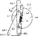
本发明的一方面包括一双位置离心枢转磁控管组件80,其说明于图2的垂直视图中,该组件依据单一旋转方向的转速可转换于两旋转半径间。该磁控管组件80包括一固定在旋转驱动轴杆62(绕该反应器的中心转轴60)上的撑座(bracket)82。该撑座82的一臂的一端由下方一枢转板84藉一枢转机构86作旋转支撑,该枢转机构可使枢转板84绕一枢转轴88枢转。该枢转板84可支撑一背板90,其由一强磁性材料组成以形成该磁控管50的磁性轭。考虑结构,该背板90可视为该枢转板84的一部份,因其与绕该枢转轴88一起枢转。一轴衬92固定在该撑座82,介于该转轴60及该枢转机构86之间;而另一轴衬94是固定于该背板90上的一安装件95。一张力弹簧96的两端接附于两轴衬92,94。一第一尼龙阻挡物100是螺附(screwed)在该撑座82一侧上的该枢转板84,而一第二尼龙阻挡物102则螺附在该撑座82另一侧上的该背板90。各阻挡物100,102包括一具有通孔的金属圆形突出物,供设螺丝及一管形的软、弹性尼龙护套,从而可安装于其外侧以缓冲对该撑座82的突然冲击及震动。弹簧96可将该具有第二阻挡物102的背板90的一侧偏压向该撑座82,并因此将该磁控管偏压向该转轴60。不过,内侧方向的枢转会受限于邻接且啮合该撑座82之第二阻挡物102。另一方面,该驱动轴杆62的旋转可施加足够的离心力于重的磁控管50及相关组件上,并将具有第二阻挡物102之该档板90的一侧以远离该转轴60之外径向方向推离该撑座82。不过,向外方向的枢转会受限于邻接且啮合该撑座82的第一阻挡物100。转速可决定是否向内弹簧偏压或向外离心力何者较占优势。One aspect of the present invention includes a dual position centrifugally pivoting magnetron assembly 80, illustrated in vertical view in FIG. 2, which is switchable between two radii of rotation depending on the rotational speed in a single direction of rotation. The magnetron assembly 80 includes a
虽然旋转驱动轴杆62的旋转与枢转板84的枢转其两者移动相当类似,但仍赋予不同名称。然而,两种移动间较明显的差异在于磁控管50是固定旋转,但于工艺期间会为大角度的360°转动选择转轴60的半径,同时枢转板84以约小于90°角改变由一者至另一者的半径位置。机械偏压的术语应可了解指一预先决定之力施加于一物体,以迫使其移向该偏压力之方向,但实际移动一般仍取决于与该移动相对的抵抗力。Although the rotation of the
平衡锤(counterweight)104固定在该撑座82的另一臂,且设计以具有如该磁控管50及相关组件般相同的惯性移动,以减少旋转期间的震动。然而,由于磁控管的惯性移动取决于其径向位置,若平衡锤受到相对于该转轴60的相同径向移动时,平衡力会改善。一位置标106(例如磁铁)固定在背板90上,且一位置感应器108(例如磁性霍尔(Hall)感应器,如图1所示)设于该转动磁控管50上方顶部,以使控制器48在该旋转磁铁106通过或未通过磁性感应器108下方时判断该磁控管的当时径向位置。A counterweight 104 is fixed to the other arm of the
在本发明的该实施例中,改变旋转驱动轴杆62的转速可使离心力克服弹簧偏压力而将该磁控管置于一第一径向外侧位置、或支配弹簧偏压力而将该磁控管50置于一第二径向内侧位置。图2所示的该磁控管位置是离心力较大所致的外侧位置(OUT position)。该外侧位置以平面方式示意性地图标在图3中,其中较为简化的表示出该枢转板84。当该旋转驱动轴杆62以够高之速率fOUT作一旋转方向的转动时,磁控管50上的离心力会大于弹簧张力,并使该枢转板84及接附磁控管50绕该撑座82的枢转轴88向外枢转。反之,在位于图4的平面图的内侧位置(IN position)时,该旋转驱动轴杆62会以相同旋转方向、但一相当低的速率fIN旋转,使弹簧96的弹簧张力大于离心力而拉动该枢转板84及接附磁控管50,以绕该枢转轴88向内枢转,移向撑座82而抵达所示的内侧位置。无论磁控管位置如何,驱动轴杆62会绕该中心转轴60持续转动该磁控管50,但该磁控管50于内侧位置的径向位移会大于外侧位置。藉此,磁控管50在其位于不同半径位置时将可扫描靶材不同区域。In this embodiment of the invention, varying the speed of rotation of the
参照图5说明磁控管移动的运动。线条110、111、112示出了施于枢转板84上的力矩(即以重的磁控管50绕该枢转轴88所施加的离心力)与枢转角(指该枢转板84及撑座82之间对三个旋转轴杆转速值50rpm、68rpm及85rpm的枢转角)的函数。在所示的该机构配置中始终位于向外方向的该枢转力矩随转速而增加,且当枢转板84将该磁控管50移离该转轴杆62时亦随枢转角而增加。虚线113示出了弹簧96张力绕该枢转轴88所施加的力矩与枢转角的函数。弹簧力矩始终位于内侧方向。净力矩即为离心力矩及弹簧力矩间的差,且该差值可决定该枢转板82向内或向外枢转。应注意的是离心力与弹簧力矩两者均受枢转角影响,此不仅是因为偏压的差异及改变弹簧长度与磁控管半径的离心力,也是因为改变力矩臂相对于撑座纵轴的几何所致。双稳定态操作(Bistable operation)是可以达成的,只要所选择的两转速fIN及fOUT(例如图中50rpm及68rpm)可完全涵盖该弹簧力矩113(即两阻挡物间枢转角的所有值),以让低速fIN旋转之该磁控管可旋转至内侧阻挡物,并让较高速fOUT旋转的该磁控管可旋转至外侧阻挡物。The movement of the magnetron movement will be described with reference to FIG. 5 . Lines 110, 111, 112 show the moment applied to the pivot plate 84 (i.e. the centrifugal force exerted by the
然动力学会因该相对旋转之枢转板84以及撑座82间之封闭旋转所施加的力矩(其本身是由摩擦产生且可阻碍任何移动)而更显复杂。在没有相对移动时封闭力矩具最大值,一旦开始移动才会变小。假设磁控管因撑座82抵邻该第一阻挡物100而处于稳定的外侧位置1,其在以速率fOUT=68rpm旋转时,需进一步减少会克服该封闭力矩的旋转以使转速低于平衡点(即离心力力矩等于弹簧力矩的点)。该磁控管接着会暂时处于位置2,在该处磁控管位于外侧位置但以fIN=50rpm作旋转。若50rpm低于无法克服封闭力矩的挣脱点(breakaway point)时,磁控管会在转速到达50rpm前开始移至位置3。同样的,当需要由稳定的位置3向外移动时,转速须为离心力力矩及弹簧力矩间的差距作充分提升以超过封闭力矩,藉以将磁控管暂时推向位置4,使其以68rpm转速于内侧位置旋转。该磁控管接着会快速向外移至稳定的外侧位置1。The dynamics are however further complicated by the torque exerted by the closed rotation between the relatively
该两位置间的转换在转速高于或低于其恰巧可开始移动所需的转速时可予以加速。例如,当由外侧位置移至内侧位置时,转速可由68rpm降至50rpm,以明显增加不平衡的力矩。当磁控管抵达内侧位置时,转速可降至50rpm。同样的,当由内侧位置移至外侧位置时,转速可由50rpm明显提升至高于68rpm以激活并完成移动,并于其后降至68rpm或甚至更低的转速。The transition between the two positions can be accelerated at speeds above or below the speed at which it can just begin to move. For example, when moving from the outside position to the inside position, the speed can be reduced from 68rpm to 50rpm to significantly increase the unbalanced moment. When the magnetron reaches the inner position, the speed can be reduced to 50rpm. Likewise, when moving from the inboard position to the outboard position, the speed can be increased significantly from 50 rpm to above 68 rpm to activate and complete the movement, and thereafter to drop to 68 rpm or even lower.
该磁控管移动中参照图2、3及4无流体影响下作描述,然而流体影响在转速改变时、以及在冷却水的打旋移动趋于平稳(通常在旋转撑座82及磁控管50后)之前会变得相当重要。旋转方向示出在图3及图4中,用以将磁控管50拉引通过粘性冷却水。取决增加转速的额外流体力可用以加速朝向外侧位置的移动。反之,若旋转方向与所示相反,它会将磁控管50推过液体。当转速减缓时,流体力可较快将磁控管50压向中心位置。The magnetron movement is described with reference to Figs. 2, 3 and 4 without fluid influence, but the fluid influence tends to be stable when the rotating speed changes and the swirling movement of the cooling water (usually between the
枢转机构必须按若干要求进行设计:其通常浸于冷却水中,其亦必须转动以最小的下垂及震动方式支撑重的磁控管,特别是由于磁控管可能需要旋转接近靶材背侧。该枢转机构应施加最小的封闭力矩及其它摩擦作用以降低转速的所需差值。图6中以截面图方式示出的该枢转机构86具有良好效能。至少一螺栓可将一心轴(spindle)114固定至枢转板84以与枢转轴88对准。一对以一管状间距物117分隔之经封闭润滑轴承115,116的内环是藉一凸缘118(螺附于该心轴114)安设于该心轴114上。该轴承115,116的内环并以一环形预负载弹簧(其以一藉螺栓固定在撑座82的盖体122压抵于该上方轴承115的外环的轴端)120安设于撑座82上。该含有轴承115,116的腔体系以其两端封闭于水态环境,此封闭方式乃藉由:该撑座82及盖体122间的一静态O形环封闭件124、该盖体122、以及该心轴114下方外围及该撑座82的一内延伸唇部128间的一动力封闭件126等方式为之。为降低摩擦封闭力矩,该动力封闭件126的直径应缩至最小。The pivot mechanism must be designed with several requirements: it is usually submerged in cooling water, it must also rotate to support the heavy magnetron with minimal droop and vibration, especially since the magnetron may need to rotate close to the backside of the target. The pivot mechanism should exert a minimum of closing torque and other frictional effects to reduce the desired difference in rotational speed. The pivot mechanism 86 shown in cross-section in FIG. 6 has good performance. At least one bolt may secure a spindle 114 to the
在重磁控管以及强磁性材料(如NdFeB)易脆性的情况下,尼龙阻挡物100,102的防震性仍嫌不足。因此,需要以弹簧负载吸震体替换尼龙阻挡物,其类似车用吸震体,可安装在撑座或枢转板及背板上,以更滑顺地啮合其它组件上的阻挡物。In the case of heavy magnetrons and the fragility of ferromagnetic materials (such as NdFeB), the shock resistance of the
一第一较佳实施例的不平衡、弧形磁控管139以垂直视图示出在图7中,大致来自图1及图2的底部。二十个具第一磁极性的柱形永久磁铁132沿着柱形轴配设于该背板90上一闭合的外部地带,其作为磁性轭以及一固定于该枢转板84的支撑件。十个相同设计但具有相反的第二磁极性的磁铁134则以弧形配设于该外部地带内。该外部磁性地带的磁性强度高于内侧磁性弧段两倍,以使该磁控管不平衡,如先前于Fu案专利中所讨论者。然而,为更加强该靶材外围的离子化溅射并进一步界定磁性侧的范围,靠近靶材边缘的弧形侧的不平衡程度可大于靠近中心的相反弧形侧。该外部磁铁132以一带形磁极片138覆盖,而内部磁铁134以弧形磁极片138覆盖。在磁控管130位于外侧位置且以靠近靶材圆周的位置旋转时,该带形磁极片136的平滑凸面侧140通常会与靶材的外围对齐。一类似的平滑凸面侧则设于背板90。另一方面,一小的凹侧系位于该带形磁极片136的另一侧。该凹侧可为平滑外型或形成尖端。磁极片136,138系经配置以具有大致固定的间隙,在其间可界定出一磁场区,平行于该靶材的内侧面并形成一邻近靶材正面的等离子回路。一非磁性分隔板142固定于该背板90及该磁极片136,138之间,其包括数个孔径以让磁铁132,134可适配于其中以作校准。该磁控管30的操作中心接近磁铁132,134的重心,即位于弧形内磁极片138内。A first preferred embodiment unbalanced, curved magnetron 139 is shown in FIG. 7 in vertical view, approximately from the bottom of FIGS. 1 and 2 . Twenty cylindrical
虽然磁控管130已有令人满意的效果,但在重心径向地向外转换时两磁控管位置间的运动变化会更为改善,以在磁控管径向移动时在惯性移动上有较大变化。一具有向外设置重心之磁控管150的第二实施例以分解底部垂直视图示出在图8中。非磁性校准以及重量档块152(例如非磁性不锈钢)可取代图7的分隔板142。档块152中定位销可使其与档板90及磁极片136,138对齐。螺栓154通过背板90及档块152并螺入磁极片136,138中一起固定磁控管。While the
档块152包括一重量部156,其延伸至该带形磁极片136之外凸面部140,亦即,再磁控管150位于外侧位置时是径向朝外。该重量部156的厚度大致等于磁铁长度,且除轴向通孔158(乃形成以供未示出的内部磁铁及未示出的外部磁铁的径向外半部通过)外大致连续。该档块152也包括一半环部160,其厚度较小且具有数个孔径供其余十个外磁铁132通过。The
该弧形磁控管150的重心较图7的该磁控管130靠近该平滑凸面边缘140,且也具有较少部件的简易设计以易于组装。该重量部156约2千克的额外重量可帮助两稳定位置间的移动。然而,因额外重量必须于两个不同径向位置旋转支撑在可移式悬臂结构上,故下垂及震动的问题会较图8中较轻设计明显。此外,额外重量也会增加阻挡物处的冲击。The center of gravity of the arc-shaped
弧形磁控管130或150具有一大致由两磁极片136,138间的间隙外围所界定的形状,其于一方向上的长度实质上大于另一方向。此形状有利于两步骤溅射沉积以及清洁工艺。如图9中底部平面图所示,在溅射沉积期间,该以实线示出的弧形磁控管130以其长尺寸(或称长尺寸段,即与该靶材16的圆周对齐并垂直于该旋转轴60延伸至磁控管中心的半径者)以及其短尺寸(或称短尺寸段,即大致对齐靶材半径者)邻设于该靶材16的有效边缘170。更明确而言,该外磁极136的外侧部于溅射沉积中可位于该靶材的有效边缘170上。两磁极136,138间的间隙172可大致界定出该溅射腔室内的一等离子回路,该腔室可溅射邻近等离子回路(由靶材边缘170向内径向延伸)的靶材16的环形区域。在边缘溅射的一实施例中,该等离子路径会扫描该靶材半径的外半部延伸的环形带,但不会扫描到内半部内侧的靶材。The
在溅射沉积期间,RF源28会强烈地偏压晶片18以加速溅射离子于高深宽比开孔内,而使之更均匀覆盖阻挡材料。该磁控管130很小,但绕该靶材中心60旋转以于靶材中心60周围(包括磁控管间隙172)环形带中形成相当均匀的溅射侵蚀。磁控管的小尺寸会使该环形带中的平均溅射率相对较小。然而,对高深宽比开孔中的阻挡层而言低沉积仍可接受,其需够薄以使大多数的开孔可用于铜或其它金属化。During sputter deposition, the RF source 28 strongly biases the wafer 18 to accelerate the sputtered ions within the high aspect ratio openings to more uniformly cover the barrier material. The
在清洁阶段的初期,转速会减缓且磁控管130会绕该枢转点88旋转至一位置(以虚线示出,靠近靶材中心60)。在此位置,该磁控管130的长尺寸段经对齐后与靶材圆周相比,较接近靶材16半径,因此可让靶材16的较长半径得以清洁。如图所示,长尺寸段倾斜于转轴60半径至磁控管中心约45°,但倾斜角较佳可为0°至60°。同样有利的是,在清洁位置的磁控管间距172由靶材中心60延伸至间距172,而界定出沉积位置的等离子回路。因此,于沉积步骤溅射的所有靶材径向向内区域会在清洁步骤中被溅射。在清洁步骤期间晶片偏压可甚至降为零,以最小化晶片基座处的荷能离子通量。Early in the cleaning phase, the rotational speed slows down and the
除了图2所示弹簧96外,也可使用其它类型的偏压装置。压缩弹簧可藉由将其移至撑座82的其它侧的方式取代。可使用一活动弹簧或螺旋弹簧,例如,一端固定接近该枢转轴且另一端位于枢转板84或背板90者。一轴固定于一组件的弹簧卷曲轮(spring-wound wheel)可绕覆以缆线,另一端固定于另一组件。前述该偏压装置均为被动式,然主动式偏压亦可行。In addition to the
在图10所示平面图的一离心磁控管的另一实施例中,线性滑动机构180包括该固定于该旋转驱动轴杆62并可绕该靶材中心轴60旋转的撑座82。一径向延伸狭缝182形成于该撑座82中,用以容纳并校准一椭圆形支撑柱184,其可径向滑动于该狭缝182内。该支撑柱184可支撑该撑座82下的磁控管50,同时两支撑梁186可藉由低摩擦接口将该支撑柱184滑动支撑于该撑座82上表面上。一未示出的平衡锤可接附于该撑座82的一端与该狭缝182相对,其接附乃藉由与之固定或径向移动以对应该磁控管50的移动的方式为之。两弹簧188,190两端部分别连接至一第一横臂192(固定于该撑座82)及一第二横臂194(固定于该支撑柱184),藉以将该磁控管50偏压向该靶材中心60。然而,在足够高的转速下,施加在旋转磁控管50上的离心力将足以克服偏压力,并使该磁控管以该支撑柱(啮合该狭缝162的外侧端196)的外侧端进入所示的外侧位置。然而在低转速下,偏压力可克服离心力,使磁控管以该支撑柱184(由该狭缝182之内侧端198阻挡)的内侧端移至其内侧位置。In another embodiment of a centrifugal magnetron shown in plan view in FIG. 10 , the linear slide mechanism 180 includes the
然亦可能设计出一种离心力驱动的磁控管,其可藉由偏压装置及低转速配合下移至该外侧位置,以及藉由增加之离心力于高转速下移至该内侧位置。However, it is also possible to design a centrifugally driven magnetron that can be moved down to the outboard position at low rotational speeds by a biasing device and moved down to the inboard position at high rotational speeds by increased centrifugal force.
该阻挡物具有双稳定操作效果,然而其亦可更适当的平衡施加于该偏压装置的离心力,以使磁控管可以多于两个径向位置作旋转,而无需使用中间阻挡物。The barrier has a bi-stable operating effect, however it also more properly balances the centrifugal force applied to the biasing means so that the magnetron can rotate in more than two radial positions without the use of an intermediate barrier.
调整磁控管的另一位置也可应用于本发明中。例如,Fu等人在美国专利第6,692,617号中公开了一活动控制的可调式磁控管200,其示意性截面图示出在图11中。一支撑板202固定在该旋转驱动轴杆62(沿靶材轴60延伸)的一端,以支撑该磁控管50。一支撑柱204将磁控管50支撑在旋转支撑板202上,滑动在用以导引该支撑柱204于径向方向之径向狭缝206中。一气压或液压式致动器208(其具有一连接至该支撑柱204的致动器臂)支撑在该支撑板202上,其经由该旋转轴杆62中的一液体线210驱动,并经由一未示出的旋转耦合件连接至一液体动力源。连接在该支撑柱204及该支撑板202间的一弹簧210或其它偏压装置可使用以对抗该致动器208施加至支撑柱204的力。然而,在该致动器208用以对抗离心力时,也可省略独立的偏压装置。在任何情况下,经由致动器208所施加的流体力均可以该旋转撑座82的径向方向移动该磁控管,以使磁控管位于至少两处径向位置,一位置利于边缘溅射,且另一位置则利于靶材16中心处的溅射。该活动控制的可调式磁控管200无论转速如何均可径向调整磁控管。若该可调式磁控管200具有多于两处的位置时,该磁控管50的径向位置可更精确地控制。Adjusting another position of the magnetron is also applicable in the present invention. For example, Fu et al. in US Pat. No. 6,692,617 disclose a motion-controlled
一基于致动器的设计包括图2的该枢转式弧形磁控管,其几何形状大致与双稳定模式所需相当。反之,非依靠转速的改变以控制旋转半径者,例如一外部控制致动器,其连接在该阻挡物100的顶部上以及该撑座82的一侧上(与该枢轴88相对)的各个枢轴间,并经由旋转轴杆62中的液体线210选择性供应气压力或液压力,如先前图11所述。该弹簧96也可能不需要。然而若该致动器仅凭借张力施力,弹簧可以相反方向偏压该背板90,例如,藉由连接在前述枢轴间的方式进行。然而,离心力本身即可提供所需的偏压。An actuator-based design includes the pivoting arc magnetron of FIG. 2 with a geometry roughly equivalent to that required for the bistable mode. On the contrary, those who do not rely on the change of the rotational speed to control the radius of rotation, such as an external control actuator, are connected to the top of the
其它调整机构亦为可行,例如,两共轴杆,一者控制旋转而另一者作径向调整。Rosenstein的双向离心力磁控管可用以交替于溅射沉积及靶材清洁间,然而相反方向会影响操作产量。Other adjustment mechanisms are also possible, for example two coaxial rods, one controlling the rotation and the other for radial adjustment. Rosenstein's bi-directional centrifugal force magnetrons can be used to alternate between sputter deposition and target cleaning, however the opposite orientation can impact operational throughput.
单向双位置磁控管的快速移动速度可使其用以清洁各晶片的靶材,而不会过度影响产量。该清洁可在加工处理过的晶片移出反应器后、以及新的晶片送入反应器之前实施。另一方面,仅有在一非常短溅射时间的溅射材料已存在阻挡层时才需要各晶片的清洁。因此,清洁可在晶片位于反应器中时原位(in-situ)实施。更明确而言,对一双层阻障层而言(例如TaN/Ta),其溅射可利用因低转速靠近靶材中心的磁控管而在氮存在下进行一非常短,如2或3秒的反应性溅射。在多次工艺循环后,短暂的初始内溅射应避免TaN累积在靶材中心。其后,增加的转速可将磁控管移至靶材周围同时持续溅射TaN。可利用较靠近靶材周围的磁控管进行最后的Ta溅射。The fast travel speed of the unidirectional dual position magnetron allows it to be used to clean targets on each wafer without unduly impacting throughput. This cleaning can be performed after the processed wafers are removed from the reactor and before new wafers are introduced into the reactor. On the other hand, cleaning of the individual wafers is only required if a barrier layer of sputtered material is present for a very short sputtering time. Thus, cleaning can be performed in-situ while the wafer is in the reactor. More specifically, for a double barrier layer (e.g. TaN/Ta), the sputtering can be performed in the presence of nitrogen using a magnetron close to the center of the target due to its low rotational speed for a very short period, such as 2 or 3 seconds of reactive sputtering. A brief initial in-sputter should avoid TaN accumulation in the center of the target after many process cycles. Thereafter, increased rotational speed moves the magnetron around the target while continuing to sputter TaN. The final Ta sputtering can be done with a magnetron closer to the target periphery.
虽然本发明系描述在溅射沉积及靶材清洁步骤间改变磁控管位置,但磁控管可因其它目的而移动,例如为激发等离子或为改变以作晶片的溅射蚀刻。Gung等人于2004年5月26日所申请的临时申请案第60/574,905号,以及于2004年9月23日申请的专利申请案第10/950,349号,标题为“VARIABLEQUADRUPLE ELECTROMAGNET ARRAY IN PLASMA PROCESSING”中公开了一种可配置不同操作模式的溅射反应器,其包括具控制差异的四电磁数组(quadruple electromagnet array),其等全文均合并于此以供参考。本发明也利于以一磁控管实施,以改变靶材及磁控管间的间距,如Subramani等人于2004年3月24日所申请的临时申请案第60/555,992号所公开的。Hong等人于2004年9月16日申请的美国专利申请案第10/942,273号,标题为“MECHANISMFOR VARYING THE SPACING BETWEEN SPUTTER MAGNETRON ANDTARGET”中公开了一较普遍的机构及工艺,其全文均合并于此以供参考。Although the present invention describes changing the position of the magnetron between the sputter deposition and target cleaning steps, the magnetron may be moved for other purposes, such as to energize the plasma or to change for sputter etching of the wafer. Provisional Application No. 60/574,905, filed May 26, 2004, and Patent Application No. 10/950,349, filed September 23, 2004, by Gung et al., entitled "VARIABLEEQUADRUPLE ELECTROMAGNET ARRAY IN PLASMA PROCESSING A sputtering reactor configurable for different modes of operation including a quadruple electromagnetic array with control differences is disclosed in ", which is hereby incorporated by reference in its entirety. The present invention is also advantageously implemented with a magnetron to vary the spacing between the target and the magnetron as disclosed in Provisional Application No. 60/555,992 filed March 24, 2004 by Subramani et al. U.S. Patent Application No. 10/942,273, filed September 16, 2004 by Hong et al., entitled "MECHANISMFOR VARYING THE SPACING BETWEEN SPUTTER MAGNETRON ANDTARGET", discloses a relatively general mechanism and process, the full text of which is incorporated in This is for reference.
虽然本发明所描述是关于溅射一耐火阻挡金属,特别是钽及其氮化物,但本发明也可应用于其它阻挡金属(例如钛及钨),以及用于硅化物(例如钴、镍及钼)。本发明也可应用于金属化的金属及其晶种层,特别是铝(其受到剥落的再沉积),且也可应用于铜,因其在多步骤工艺中会需要不同的溅射特性。双位置磁控管的灵活性也可用于溅射其它类型的材料,包括RF溅射金属或绝缘层。Although the present invention has been described with respect to sputtering a refractory barrier metal, particularly tantalum and its nitrides, the present invention is also applicable to other barrier metals such as titanium and tungsten, and to silicides such as cobalt, nickel and molybdenum). The invention is also applicable to metallized metals and their seed layers, in particular aluminum (which is subject to exfoliated redeposition), and also to copper, which would require different sputtering characteristics in a multi-step process. The flexibility of the two-position magnetron can also be used to sputter other types of materials, including RF sputtering metals or insulating layers.
本发明可额外控制溅射及靶材清洁,且通过略为改变磁控管扫描机构使其易于结合目前反应器设计的方式即可控制地改变溅射特性。The present invention provides additional control over sputtering and target cleaning, and can controllably alter sputtering characteristics by slightly altering the magnetron scanning mechanism in such a way that it can be easily incorporated into current reactor designs.
Claims (35)
Applications Claiming Priority (5)
| Application Number | Priority Date | Filing Date | Title |
|---|---|---|---|
| US55599204P | 2004-03-24 | 2004-03-24 | |
| US60/555,992 | 2004-03-24 | ||
| US10/949,735 | 2004-09-23 | ||
| US10/949,735US7018515B2 (en) | 2004-03-24 | 2004-09-23 | Selectable dual position magnetron |
| PCT/US2005/008513WO2005100630A1 (en) | 2004-03-24 | 2005-03-15 | Selectable dual position magnetron |
Publications (2)
| Publication Number | Publication Date |
|---|---|
| CN1914351Atrue CN1914351A (en) | 2007-02-14 |
| CN1914351B CN1914351B (en) | 2010-12-15 |
Family
ID=34988468
Family Applications (1)
| Application Number | Title | Priority Date | Filing Date |
|---|---|---|---|
| CN2005800038296AExpired - LifetimeCN1914351B (en) | 2004-03-24 | 2005-03-15 | Selectable dual position magnetron |
Country Status (5)
| Country | Link |
|---|---|
| US (3) | US7018515B2 (en) |
| JP (1) | JP4948391B2 (en) |
| CN (1) | CN1914351B (en) |
| TW (1) | TWI314585B (en) |
| WO (1) | WO2005100630A1 (en) |
Cited By (14)
| Publication number | Priority date | Publication date | Assignee | Title |
|---|---|---|---|---|
| CN102560387A (en)* | 2010-12-10 | 2012-07-11 | 北京北方微电子基地设备工艺研究中心有限责任公司 | Magnetic control source, magnetron sputtering equipment and magnetron sputtering method |
| CN102737928A (en)* | 2011-04-02 | 2012-10-17 | 北京北方微电子基地设备工艺研究中心有限责任公司 | Magnetic pole component, magnetron provided with magnetic pole component, sputtering chamber apparatus, and substrate processing device |
| CN103422065A (en)* | 2012-05-16 | 2013-12-04 | 北京北方微电子基地设备工艺研究中心有限责任公司 | Magnetron sputtering device and magnetron control method |
| CN103681975A (en)* | 2013-12-27 | 2014-03-26 | 柳州百韧特先进材料有限公司 | Method for manufacturing CIGS solar cell |
| TWI457456B (en)* | 2008-10-15 | 2014-10-21 | Applied Materials Inc | Control of erosion profile on a dielectric rf sputter target |
| CN104746027A (en)* | 2013-12-29 | 2015-07-01 | 北京北方微电子基地设备工艺研究中心有限责任公司 | Magnetron component and magnetron sputtering device |
| CN104969331A (en)* | 2013-02-07 | 2015-10-07 | 应用材料公司 | Physical Vapor Deposition RF DC Open/Closed Loop Optional Magnetron |
| CN106702336A (en)* | 2015-11-16 | 2017-05-24 | 北京北方微电子基地设备工艺研究中心有限责任公司 | Installation mechanism of magnetron and magnetron sputtering equipment |
| WO2018210120A1 (en)* | 2017-05-18 | 2018-11-22 | 北京北方华创微电子装备有限公司 | Magnetron driving mechanism, magnetron assembly, and reaction chamber |
| CN109830418A (en)* | 2017-11-23 | 2019-05-31 | 北京北方华创微电子装备有限公司 | For driving sweep mechanism, magnetic control source and the magnetron sputtering apparatus of magnetron |
| CN109837518A (en)* | 2017-11-28 | 2019-06-04 | 北京北方华创微电子装备有限公司 | Deposition ring fixation kit, bogey and reaction chamber |
| CN111033683A (en)* | 2017-07-17 | 2020-04-17 | 应用材料公司 | Cathode assembly with dual position magnetron and central coolant supply |
| WO2021213273A1 (en)* | 2020-04-24 | 2021-10-28 | 北京北方华创微电子装备有限公司 | Semiconductor processing device and magnetron mechanism thereof |
| CN114156149A (en)* | 2021-11-25 | 2022-03-08 | 北京北方华创微电子装备有限公司 | Magnetron device and semiconductor processing equipment |
Families Citing this family (69)
| Publication number | Priority date | Publication date | Assignee | Title |
|---|---|---|---|---|
| KR100846484B1 (en)* | 2002-03-14 | 2008-07-17 | 삼성전자주식회사 | RMIM electrode, manufacturing method thereof and sputtering apparatus employing the same |
| US7910218B2 (en) | 2003-10-22 | 2011-03-22 | Applied Materials, Inc. | Cleaning and refurbishing chamber components having metal coatings |
| US9771648B2 (en) | 2004-08-13 | 2017-09-26 | Zond, Inc. | Method of ionized physical vapor deposition sputter coating high aspect-ratio structures |
| US7018515B2 (en)* | 2004-03-24 | 2006-03-28 | Applied Materials, Inc. | Selectable dual position magnetron |
| US7670436B2 (en) | 2004-11-03 | 2010-03-02 | Applied Materials, Inc. | Support ring assembly |
| US8617672B2 (en) | 2005-07-13 | 2013-12-31 | Applied Materials, Inc. | Localized surface annealing of components for substrate processing chambers |
| US7762114B2 (en) | 2005-09-09 | 2010-07-27 | Applied Materials, Inc. | Flow-formed chamber component having a textured surface |
| US8021527B2 (en) | 2005-09-14 | 2011-09-20 | Applied Materials, Inc. | Coaxial shafts for radial positioning of rotating magnetron |
| US9127362B2 (en) | 2005-10-31 | 2015-09-08 | Applied Materials, Inc. | Process kit and target for substrate processing chamber |
| US8647484B2 (en) | 2005-11-25 | 2014-02-11 | Applied Materials, Inc. | Target for sputtering chamber |
| US20070209925A1 (en)* | 2006-03-09 | 2007-09-13 | Applied Materials, Inc. | Etch and sidewall selectivity in plasma sputtering |
| KR101213103B1 (en)* | 2006-06-30 | 2013-01-09 | 엘지디스플레이 주식회사 | bonding device and fa brication method of Light emitting device using thereof |
| KR100910673B1 (en)* | 2006-08-04 | 2009-08-04 | 어플라이드 머티어리얼스, 인코포레이티드 | Ganged scanning of multiple magnetrons, especially two level folded magnetrons |
| US8557094B2 (en)* | 2006-10-05 | 2013-10-15 | Applied Materials, Inc. | Sputtering chamber having auxiliary backside magnet to improve etch uniformity and magnetron producing sustained self sputtering of ruthenium and tantalum |
| US8500963B2 (en)* | 2006-10-26 | 2013-08-06 | Applied Materials, Inc. | Sputtering of thermally resistive materials including metal chalcogenides |
| US7767064B2 (en) | 2006-10-27 | 2010-08-03 | Applied Materials, Inc. | Position controlled dual magnetron |
| US7981262B2 (en) | 2007-01-29 | 2011-07-19 | Applied Materials, Inc. | Process kit for substrate processing chamber |
| US7659204B2 (en)* | 2007-03-26 | 2010-02-09 | Applied Materials, Inc. | Oxidized barrier layer |
| US20080296142A1 (en)* | 2007-05-29 | 2008-12-04 | Hien-Minh Huu Le | Swinging magnets to improve target utilization |
| US7942969B2 (en) | 2007-05-30 | 2011-05-17 | Applied Materials, Inc. | Substrate cleaning chamber and components |
| US8202798B2 (en)* | 2007-09-20 | 2012-06-19 | Freescale Semiconductor, Inc. | Improvements for reducing electromigration effect in an integrated circuit |
| US8114256B2 (en) | 2007-11-30 | 2012-02-14 | Applied Materials, Inc. | Control of arbitrary scan path of a rotating magnetron |
| CA2708995C (en)* | 2007-12-13 | 2018-03-20 | Wutpool, Inc. | Retractable load-bearing cover |
| US8133360B2 (en)* | 2007-12-20 | 2012-03-13 | Applied Materials, Inc. | Prediction and compensation of erosion in a magnetron sputtering target |
| KR101258882B1 (en)* | 2008-02-13 | 2013-04-29 | 가부시키가이샤 소니 디에이디씨 | Magnetron sputtering apparatus and magnetron sputtering method |
| US20090308739A1 (en)* | 2008-06-17 | 2009-12-17 | Applied Materials, Inc. | Wafer processing deposition shielding components |
| KR20200093084A (en)* | 2008-06-17 | 2020-08-04 | 어플라이드 머티어리얼스, 인코포레이티드 | Apparatus and method for uniform deposition |
| US8992741B2 (en)* | 2008-08-08 | 2015-03-31 | Applied Materials, Inc. | Method for ultra-uniform sputter deposition using simultaneous RF and DC power on target |
| US20100096255A1 (en)* | 2008-10-22 | 2010-04-22 | Applied Materials, Inc. | Gap fill improvement methods for phase-change materials |
| US9771647B1 (en)* | 2008-12-08 | 2017-09-26 | Michael A. Scobey | Cathode assemblies and sputtering systems |
| US8137517B1 (en) | 2009-02-10 | 2012-03-20 | Wd Media, Inc. | Dual position DC magnetron assembly |
| KR20120004502A (en)* | 2009-04-03 | 2012-01-12 | 어플라이드 머티어리얼스, 인코포레이티드 | High pressure RF-DC sputtering and method for improving step applicability and film uniformity of this process |
| TW201137149A (en)* | 2010-04-21 | 2011-11-01 | Hon Hai Prec Ind Co Ltd | Magnetron sputtering device |
| CN101831617B (en)* | 2010-05-28 | 2012-09-05 | 西安交通大学 | Basal plate retainer for ECR (Equivalent Continuous Rating) plasma sputtering device |
| CN102906302B (en)* | 2010-06-03 | 2015-01-28 | 株式会社爱发科 | Sputter deposition device |
| CN102534529B (en)* | 2010-12-24 | 2015-04-15 | 北京北方微电子基地设备工艺研究中心有限责任公司 | Magnetron sputtering source and magnetron sputtering equipment |
| US20120181166A1 (en)* | 2011-01-14 | 2012-07-19 | Applied Materials, Inc. | Pvd process with synchronized process parameters and magnet position |
| US9347129B2 (en)* | 2011-12-09 | 2016-05-24 | Seagate Technology Llc | Interchangeable magnet pack |
| US10573500B2 (en) | 2011-12-09 | 2020-02-25 | Seagate Technology Llc | Interchangeable magnet pack |
| CN103184420B (en)* | 2011-12-28 | 2014-12-17 | 北京北方微电子基地设备工艺研究中心有限责任公司 | Scanning mechanism for driving magnetron, magnetron sputtering source and magnetron sputtering equipment |
| US9093252B2 (en)* | 2012-02-16 | 2015-07-28 | Taiwan Semiconductor Manufacturing Co., Ltd. | Rotation plus vibration magnet for magnetron sputtering apparatus |
| US8674327B1 (en) | 2012-05-10 | 2014-03-18 | WD Media, LLC | Systems and methods for uniformly implanting materials on substrates using directed magnetic fields |
| DE102012211664A1 (en)* | 2012-07-04 | 2014-01-09 | Von Ardenne Anlagentechnik Gmbh | Magnetron sputtering device, used to perform vacuum-based physical vapor deposition for coating substrate with target material, includes magnet assembly that concentrates plasma over target surface and comprises hydraulic actuator |
| US9281167B2 (en) | 2013-02-26 | 2016-03-08 | Applied Materials, Inc. | Variable radius dual magnetron |
| US9051638B2 (en)* | 2013-03-01 | 2015-06-09 | Poole Ventura, Inc. | In-situ sputtering apparatus |
| WO2014143078A1 (en)* | 2013-03-15 | 2014-09-18 | Poole Ventura, Inc. | In-situ sputtering apparatus |
| JP6480445B2 (en)* | 2013-08-14 | 2019-03-13 | アプライド マテリアルズ インコーポレイテッドApplied Materials,Incorporated | Encapsulated magnetron |
| US9831075B2 (en) | 2013-09-17 | 2017-11-28 | Applied Materials, Inc. | Source magnet for improved resputtering uniformity in direct current (DC) physical vapor deposition (PVD) processes |
| US9581510B1 (en) | 2013-12-16 | 2017-02-28 | Western Digital Technologies, Inc. | Sputter chamber pressure gauge with vibration absorber |
| US10727122B2 (en) | 2014-12-08 | 2020-07-28 | International Business Machines Corporation | Self-aligned via interconnect structures |
| JP6471000B2 (en)* | 2015-02-24 | 2019-02-13 | 株式会社アルバック | Magnet unit for magnetron sputtering apparatus and sputtering method using this magnet unit |
| US10858727B2 (en)* | 2016-08-19 | 2020-12-08 | Applied Materials, Inc. | High density, low stress amorphous carbon film, and process and equipment for its deposition |
| US10748571B2 (en) | 2017-08-09 | 2020-08-18 | Seagate Technology Llc | Mechanically balanced and magnetically unbalanced device |
| US11024490B2 (en)* | 2017-12-11 | 2021-06-01 | Applied Materials, Inc. | Magnetron having enhanced target cooling configuration |
| CN108231509B (en)* | 2017-12-31 | 2024-03-22 | 中国电子科技集团公司第十二研究所 | Magnetron tuning device and magnetron |
| TWI850717B (en)* | 2018-06-19 | 2024-08-01 | 美商應用材料股份有限公司 | Deposition system with a multi-cathode |
| US11345991B2 (en) | 2018-09-27 | 2022-05-31 | Taiwan Semiconductor Manufacturing Company, Ltd. | Semiconductor device, method and machine of manufacture |
| US11462394B2 (en)* | 2018-09-28 | 2022-10-04 | Taiwan Semiconductor Manufacturing Co., Ltd. | Physical vapor deposition apparatus and method thereof |
| US11295938B2 (en)* | 2020-06-30 | 2022-04-05 | Applied Materials, Inc. | Multi-radius magnetron for physical vapor deposition (PVD) and methods of use thereof |
| US11479847B2 (en) | 2020-10-14 | 2022-10-25 | Alluxa, Inc. | Sputtering system with a plurality of cathode assemblies |
| TWI787823B (en)* | 2021-05-17 | 2022-12-21 | 天虹科技股份有限公司 | Shielding mechanism and substrate processing chamber with shielding mechanism for decreasing particle |
| US20220384194A1 (en)* | 2021-05-28 | 2022-12-01 | Applied Materials, Inc. | Apparatus for generating magnetic fields on substrates during semiconductor processing |
| US12027352B2 (en)* | 2021-05-28 | 2024-07-02 | Applied Materials, Inc. | Apparatus for generating magnetic fields on substrates during semiconductor processing |
| TWI788871B (en)* | 2021-06-07 | 2023-01-01 | 台灣積體電路製造股份有限公司 | Method of forming semiconductor device and method of performing physical deposition process |
| CN113445013B (en)* | 2021-06-28 | 2022-06-03 | 哈尔滨工业大学 | High-power magnetron sputtering film deposition device and method for inner wall of rotor bearing inner ring |
| CN115679278B (en)* | 2021-07-29 | 2025-01-14 | 北京北方华创微电子装备有限公司 | Dual magnetron sputtering device and semiconductor process equipment |
| WO2023069158A1 (en) | 2021-10-21 | 2023-04-27 | Applied Materials, Inc. | Apparatus for generating magnetic fields on substrates during semiconductor processing |
| CN114774872B (en)* | 2022-04-29 | 2023-09-08 | 北京北方华创微电子装备有限公司 | Magnetron device and magnetron sputtering equipment |
| CN115418617B (en)* | 2022-05-30 | 2023-10-13 | 北京北方华创微电子装备有限公司 | Process chamber of semiconductor process equipment and magnetron sputtering assembly thereof |
Family Cites Families (21)
| Publication number | Priority date | Publication date | Assignee | Title |
|---|---|---|---|---|
| US4714536A (en)* | 1985-08-26 | 1987-12-22 | Varian Associates, Inc. | Planar magnetron sputtering device with combined circumferential and radial movement of magnetic fields |
| EP0283095A1 (en)* | 1987-03-16 | 1988-09-21 | Hauzer Holding B.V. | Method and arrangement for mechanically moving of a magnetic field generating device in a cathode arc discharge evaporating device |
| US5618388A (en) | 1988-02-08 | 1997-04-08 | Optical Coating Laboratory, Inc. | Geometries and configurations for magnetron sputtering apparatus |
| US4995958A (en) | 1989-05-22 | 1991-02-26 | Varian Associates, Inc. | Sputtering apparatus with a rotating magnet array having a geometry for specified target erosion profile |
| US5171415A (en)* | 1990-12-21 | 1992-12-15 | Novellus Systems, Inc. | Cooling method and apparatus for magnetron sputtering |
| US5188717A (en)* | 1991-09-12 | 1993-02-23 | Novellus Systems, Inc. | Sweeping method and magnet track apparatus for magnetron sputtering |
| JPH07226398A (en)* | 1994-02-10 | 1995-08-22 | Fujitsu Ltd | Target sputtering method and cleaning method |
| JP3935231B2 (en)* | 1996-09-18 | 2007-06-20 | キヤノンアネルバ株式会社 | Sputtering equipment |
| US6254747B1 (en) | 1996-12-25 | 2001-07-03 | Nihon Shinku Gijutsu Kabushiki Kaisha | Magnetron sputtering source enclosed by a mirror-finished metallic cover |
| US6692617B1 (en) | 1997-05-08 | 2004-02-17 | Applied Materials, Inc. | Sustained self-sputtering reactor having an increased density plasma |
| US6013159A (en)* | 1997-11-16 | 2000-01-11 | Applied Materials, Inc. | Particle trap in a magnetron sputtering chamber |
| US6306265B1 (en) | 1999-02-12 | 2001-10-23 | Applied Materials, Inc. | High-density plasma for ionized metal deposition capable of exciting a plasma wave |
| US6440282B1 (en)* | 1999-07-06 | 2002-08-27 | Applied Materials, Inc. | Sputtering reactor and method of using an unbalanced magnetron |
| US6228236B1 (en)* | 1999-10-22 | 2001-05-08 | Applied Materials, Inc. | Sputter magnetron having two rotation diameters |
| US6338236B1 (en)* | 2000-06-14 | 2002-01-15 | Henry Rodriguez | Mechanized harvesting machine with rotating picking elements |
| GB0207530D0 (en) | 2002-04-02 | 2002-05-08 | Univ Nottingham | High field strength microwave production and microwave processing of materials e.g. weakening of multi-phase materials |
| US6841050B2 (en) | 2002-05-21 | 2005-01-11 | Applied Materials, Inc. | Small planetary magnetron |
| US6852202B2 (en) | 2002-05-21 | 2005-02-08 | Applied Materials, Inc. | Small epicyclic magnetron with controlled radial sputtering profile |
| US7018515B2 (en)* | 2004-03-24 | 2006-03-28 | Applied Materials, Inc. | Selectable dual position magnetron |
| US20050274610A1 (en) | 2004-05-25 | 2005-12-15 | Victor Company Of Japan, Limited | Magnetron sputtering apparatus |
| US8021527B2 (en)* | 2005-09-14 | 2011-09-20 | Applied Materials, Inc. | Coaxial shafts for radial positioning of rotating magnetron |
- 2004
- 2004-09-23USUS10/949,735patent/US7018515B2/ennot_activeExpired - Lifetime
- 2005
- 2005-03-14TWTW094107743Apatent/TWI314585B/ennot_activeIP Right Cessation
- 2005-03-15JPJP2007505006Apatent/JP4948391B2/ennot_activeExpired - Lifetime
- 2005-03-15WOPCT/US2005/008513patent/WO2005100630A1/enactiveApplication Filing
- 2005-03-15CNCN2005800038296Apatent/CN1914351B/ennot_activeExpired - Lifetime
- 2005-09-14USUS11/226,858patent/US7736473B2/enactiveActive
- 2010
- 2010-06-04USUS12/794,452patent/US8685215B2/enactiveActive
Cited By (26)
| Publication number | Priority date | Publication date | Assignee | Title |
|---|---|---|---|---|
| TWI457456B (en)* | 2008-10-15 | 2014-10-21 | Applied Materials Inc | Control of erosion profile on a dielectric rf sputter target |
| CN102560387A (en)* | 2010-12-10 | 2012-07-11 | 北京北方微电子基地设备工艺研究中心有限责任公司 | Magnetic control source, magnetron sputtering equipment and magnetron sputtering method |
| CN102560387B (en)* | 2010-12-10 | 2014-05-28 | 北京北方微电子基地设备工艺研究中心有限责任公司 | Magnetic control source, magnetron sputtering equipment and magnetron sputtering method |
| CN102737928A (en)* | 2011-04-02 | 2012-10-17 | 北京北方微电子基地设备工艺研究中心有限责任公司 | Magnetic pole component, magnetron provided with magnetic pole component, sputtering chamber apparatus, and substrate processing device |
| CN102737928B (en)* | 2011-04-02 | 2014-12-17 | 北京北方微电子基地设备工艺研究中心有限责任公司 | Magnetic pole component, magnetron provided with magnetic pole component, sputtering chamber apparatus, and substrate processing device |
| CN103422065B (en)* | 2012-05-16 | 2016-08-31 | 北京北方微电子基地设备工艺研究中心有限责任公司 | magnetron sputtering apparatus and magnetron control method |
| CN103422065A (en)* | 2012-05-16 | 2013-12-04 | 北京北方微电子基地设备工艺研究中心有限责任公司 | Magnetron sputtering device and magnetron control method |
| CN104969331A (en)* | 2013-02-07 | 2015-10-07 | 应用材料公司 | Physical Vapor Deposition RF DC Open/Closed Loop Optional Magnetron |
| CN104969331B (en)* | 2013-02-07 | 2017-11-03 | 应用材料公司 | The optional magnetron of physical vapour deposition (PVD) radio frequency direct current open closed loop |
| CN103681975A (en)* | 2013-12-27 | 2014-03-26 | 柳州百韧特先进材料有限公司 | Method for manufacturing CIGS solar cell |
| CN104746027A (en)* | 2013-12-29 | 2015-07-01 | 北京北方微电子基地设备工艺研究中心有限责任公司 | Magnetron component and magnetron sputtering device |
| CN106702336B (en)* | 2015-11-16 | 2019-02-19 | 北京北方华创微电子装备有限公司 | The installing mechanism and magnetron sputtering apparatus of magnetron |
| CN106702336A (en)* | 2015-11-16 | 2017-05-24 | 北京北方微电子基地设备工艺研究中心有限责任公司 | Installation mechanism of magnetron and magnetron sputtering equipment |
| WO2018210120A1 (en)* | 2017-05-18 | 2018-11-22 | 北京北方华创微电子装备有限公司 | Magnetron driving mechanism, magnetron assembly, and reaction chamber |
| TWI692541B (en)* | 2017-05-18 | 2020-05-01 | 大陸商北京北方華創微電子裝備有限公司 | Magnetron drive mechanism, magnetron assembly and reaction chamber |
| US11282682B2 (en) | 2017-05-18 | 2022-03-22 | Beijing Naura Microelectronics Equipment Co., Ltd. | Magnetron drive mechanism, magnetron assembly and reaction chamber |
| CN111033683A (en)* | 2017-07-17 | 2020-04-17 | 应用材料公司 | Cathode assembly with dual position magnetron and central coolant supply |
| CN111033683B (en)* | 2017-07-17 | 2023-04-18 | 应用材料公司 | Cathode assembly with dual position magnetron and center fed coolant |
| CN109830418A (en)* | 2017-11-23 | 2019-05-31 | 北京北方华创微电子装备有限公司 | For driving sweep mechanism, magnetic control source and the magnetron sputtering apparatus of magnetron |
| CN109837518A (en)* | 2017-11-28 | 2019-06-04 | 北京北方华创微电子装备有限公司 | Deposition ring fixation kit, bogey and reaction chamber |
| CN109837518B (en)* | 2017-11-28 | 2021-06-08 | 北京北方华创微电子装备有限公司 | Deposition ring fixing assembly, bearing device and reaction chamber |
| WO2021213273A1 (en)* | 2020-04-24 | 2021-10-28 | 北京北方华创微电子装备有限公司 | Semiconductor processing device and magnetron mechanism thereof |
| US12249496B2 (en) | 2020-04-24 | 2025-03-11 | Beijing Naura Microelectronics Equipment Co., Ltd. | Semiconductor processing apparatus and magnetron mechanism |
| CN114156149A (en)* | 2021-11-25 | 2022-03-08 | 北京北方华创微电子装备有限公司 | Magnetron device and semiconductor processing equipment |
| WO2023092869A1 (en)* | 2021-11-25 | 2023-06-01 | 北京北方华创微电子装备有限公司 | Magnetron device and semiconductor processing apparatus |
| CN114156149B (en)* | 2021-11-25 | 2024-05-17 | 北京北方华创微电子装备有限公司 | Magnetron device and semiconductor process equipment |
Also Published As
| Publication number | Publication date |
|---|---|
| JP2007530787A (en) | 2007-11-01 |
| US7018515B2 (en) | 2006-03-28 |
| US7736473B2 (en) | 2010-06-15 |
| JP4948391B2 (en) | 2012-06-06 |
| TWI314585B (en) | 2009-09-11 |
| US20050211548A1 (en) | 2005-09-29 |
| US20100243440A1 (en) | 2010-09-30 |
| TW200602508A (en) | 2006-01-16 |
| WO2005100630A1 (en) | 2005-10-27 |
| US8685215B2 (en) | 2014-04-01 |
| US20060076232A1 (en) | 2006-04-13 |
| CN1914351B (en) | 2010-12-15 |
Similar Documents
| Publication | Publication Date | Title |
|---|---|---|
| CN1914351A (en) | Selectable dual position magnetron | |
| US7767064B2 (en) | Position controlled dual magnetron | |
| US6228236B1 (en) | Sputter magnetron having two rotation diameters | |
| JP4606162B2 (en) | Small planetary magnetron | |
| US20050133361A1 (en) | Compensation of spacing between magnetron and sputter target | |
| US7556718B2 (en) | Highly ionized PVD with moving magnetic field envelope for uniform coverage of feature structure and wafer | |
| WO2010115128A2 (en) | High pressure rf-dc sputtering and methods to improve film uniformity and step-coverage of this process | |
| US9281167B2 (en) | Variable radius dual magnetron | |
| US11688591B2 (en) | Physical vapor deposition apparatus and method thereof | |
| KR100972812B1 (en) | Selectable Dual Position Magnetron | |
| JP2005232554A (en) | Sputtering system |
Legal Events
| Date | Code | Title | Description |
|---|---|---|---|
| C06 | Publication | ||
| PB01 | Publication | ||
| C10 | Entry into substantive examination | ||
| SE01 | Entry into force of request for substantive examination | ||
| C14 | Grant of patent or utility model | ||
| GR01 | Patent grant | ||
| C56 | Change in the name or address of the patentee | ||
| CP01 | Change in the name or title of a patent holder | Address after:California, USA Patentee after:APPLIED MATERIALS, Inc. Address before:California, USA Patentee before:APPLIED MATERIALS, Inc. | |
| CX01 | Expiry of patent term | Granted publication date:20101215 | |
| CX01 | Expiry of patent term |