CN1908789B - Liquid crystal display device - Google Patents
Liquid crystal display deviceDownload PDFInfo
- Publication number
- CN1908789B CN1908789BCN2006101083647ACN200610108364ACN1908789BCN 1908789 BCN1908789 BCN 1908789BCN 2006101083647 ACN2006101083647 ACN 2006101083647ACN 200610108364 ACN200610108364 ACN 200610108364ACN 1908789 BCN1908789 BCN 1908789B
- Authority
- CN
- China
- Prior art keywords
- electrode
- sub
- storage
- subpixel
- pixel
- Prior art date
- Legal status (The legal status is an assumption and is not a legal conclusion. Google has not performed a legal analysis and makes no representation as to the accuracy of the status listed.)
- Expired - Fee Related
Links
Images


Classifications
- G—PHYSICS
- G02—OPTICS
- G02F—OPTICAL DEVICES OR ARRANGEMENTS FOR THE CONTROL OF LIGHT BY MODIFICATION OF THE OPTICAL PROPERTIES OF THE MEDIA OF THE ELEMENTS INVOLVED THEREIN; NON-LINEAR OPTICS; FREQUENCY-CHANGING OF LIGHT; OPTICAL LOGIC ELEMENTS; OPTICAL ANALOGUE/DIGITAL CONVERTERS
- G02F1/00—Devices or arrangements for the control of the intensity, colour, phase, polarisation or direction of light arriving from an independent light source, e.g. switching, gating or modulating; Non-linear optics
- G02F1/01—Devices or arrangements for the control of the intensity, colour, phase, polarisation or direction of light arriving from an independent light source, e.g. switching, gating or modulating; Non-linear optics for the control of the intensity, phase, polarisation or colour
- G02F1/13—Devices or arrangements for the control of the intensity, colour, phase, polarisation or direction of light arriving from an independent light source, e.g. switching, gating or modulating; Non-linear optics for the control of the intensity, phase, polarisation or colour based on liquid crystals, e.g. single liquid crystal display cells
- G02F1/133—Constructional arrangements; Operation of liquid crystal cells; Circuit arrangements
- G02F1/1333—Constructional arrangements; Manufacturing methods
- G02F1/1343—Electrodes
- G—PHYSICS
- G02—OPTICS
- G02F—OPTICAL DEVICES OR ARRANGEMENTS FOR THE CONTROL OF LIGHT BY MODIFICATION OF THE OPTICAL PROPERTIES OF THE MEDIA OF THE ELEMENTS INVOLVED THEREIN; NON-LINEAR OPTICS; FREQUENCY-CHANGING OF LIGHT; OPTICAL LOGIC ELEMENTS; OPTICAL ANALOGUE/DIGITAL CONVERTERS
- G02F1/00—Devices or arrangements for the control of the intensity, colour, phase, polarisation or direction of light arriving from an independent light source, e.g. switching, gating or modulating; Non-linear optics
- G02F1/01—Devices or arrangements for the control of the intensity, colour, phase, polarisation or direction of light arriving from an independent light source, e.g. switching, gating or modulating; Non-linear optics for the control of the intensity, phase, polarisation or colour
- G02F1/13—Devices or arrangements for the control of the intensity, colour, phase, polarisation or direction of light arriving from an independent light source, e.g. switching, gating or modulating; Non-linear optics for the control of the intensity, phase, polarisation or colour based on liquid crystals, e.g. single liquid crystal display cells
- G02F1/137—Devices or arrangements for the control of the intensity, colour, phase, polarisation or direction of light arriving from an independent light source, e.g. switching, gating or modulating; Non-linear optics for the control of the intensity, phase, polarisation or colour based on liquid crystals, e.g. single liquid crystal display cells characterised by the electro-optical or magneto-optical effect, e.g. field-induced phase transition, orientation effect, guest-host interaction or dynamic scattering
- G02F1/139—Devices or arrangements for the control of the intensity, colour, phase, polarisation or direction of light arriving from an independent light source, e.g. switching, gating or modulating; Non-linear optics for the control of the intensity, phase, polarisation or colour based on liquid crystals, e.g. single liquid crystal display cells characterised by the electro-optical or magneto-optical effect, e.g. field-induced phase transition, orientation effect, guest-host interaction or dynamic scattering based on orientation effects in which the liquid crystal remains transparent
- G02F1/1393—Devices or arrangements for the control of the intensity, colour, phase, polarisation or direction of light arriving from an independent light source, e.g. switching, gating or modulating; Non-linear optics for the control of the intensity, phase, polarisation or colour based on liquid crystals, e.g. single liquid crystal display cells characterised by the electro-optical or magneto-optical effect, e.g. field-induced phase transition, orientation effect, guest-host interaction or dynamic scattering based on orientation effects in which the liquid crystal remains transparent the birefringence of the liquid crystal being electrically controlled, e.g. ECB-, DAP-, HAN-, PI-LC cells
- G—PHYSICS
- G02—OPTICS
- G02F—OPTICAL DEVICES OR ARRANGEMENTS FOR THE CONTROL OF LIGHT BY MODIFICATION OF THE OPTICAL PROPERTIES OF THE MEDIA OF THE ELEMENTS INVOLVED THEREIN; NON-LINEAR OPTICS; FREQUENCY-CHANGING OF LIGHT; OPTICAL LOGIC ELEMENTS; OPTICAL ANALOGUE/DIGITAL CONVERTERS
- G02F1/00—Devices or arrangements for the control of the intensity, colour, phase, polarisation or direction of light arriving from an independent light source, e.g. switching, gating or modulating; Non-linear optics
- G02F1/01—Devices or arrangements for the control of the intensity, colour, phase, polarisation or direction of light arriving from an independent light source, e.g. switching, gating or modulating; Non-linear optics for the control of the intensity, phase, polarisation or colour
- G02F1/13—Devices or arrangements for the control of the intensity, colour, phase, polarisation or direction of light arriving from an independent light source, e.g. switching, gating or modulating; Non-linear optics for the control of the intensity, phase, polarisation or colour based on liquid crystals, e.g. single liquid crystal display cells
- G02F1/133—Constructional arrangements; Operation of liquid crystal cells; Circuit arrangements
- G02F1/1333—Constructional arrangements; Manufacturing methods
- G02F1/1343—Electrodes
- G02F1/134309—Electrodes characterised by their geometrical arrangement
- G—PHYSICS
- G02—OPTICS
- G02F—OPTICAL DEVICES OR ARRANGEMENTS FOR THE CONTROL OF LIGHT BY MODIFICATION OF THE OPTICAL PROPERTIES OF THE MEDIA OF THE ELEMENTS INVOLVED THEREIN; NON-LINEAR OPTICS; FREQUENCY-CHANGING OF LIGHT; OPTICAL LOGIC ELEMENTS; OPTICAL ANALOGUE/DIGITAL CONVERTERS
- G02F1/00—Devices or arrangements for the control of the intensity, colour, phase, polarisation or direction of light arriving from an independent light source, e.g. switching, gating or modulating; Non-linear optics
- G02F1/01—Devices or arrangements for the control of the intensity, colour, phase, polarisation or direction of light arriving from an independent light source, e.g. switching, gating or modulating; Non-linear optics for the control of the intensity, phase, polarisation or colour
- G02F1/13—Devices or arrangements for the control of the intensity, colour, phase, polarisation or direction of light arriving from an independent light source, e.g. switching, gating or modulating; Non-linear optics for the control of the intensity, phase, polarisation or colour based on liquid crystals, e.g. single liquid crystal display cells
- G02F1/133—Constructional arrangements; Operation of liquid crystal cells; Circuit arrangements
- G02F1/1333—Constructional arrangements; Manufacturing methods
- G02F1/1343—Electrodes
- G02F1/13439—Electrodes characterised by their electrical, optical, physical properties; materials therefor; method of making
Landscapes
- Physics & Mathematics (AREA)
- Nonlinear Science (AREA)
- Chemical & Material Sciences (AREA)
- Crystallography & Structural Chemistry (AREA)
- General Physics & Mathematics (AREA)
- Optics & Photonics (AREA)
- Mathematical Physics (AREA)
- Geometry (AREA)
- Liquid Crystal (AREA)
Abstract
Translated fromChinese
Description
Translated fromChinese技术领域Technical field
本发明涉及一种液晶显示器(LCD),更具体地讲,涉及一种垂直取向的LCD。The present invention relates to a liquid crystal display (LCD), and more particularly, to a vertically oriented LCD.
背景技术 Background technique
液晶显示器(LCD)是最广泛使用的平板显示器之一。通常,LCD包括设置有场发生电极如像素电极和共电极的两个基底以及置于这两个基底之间的液晶(LC)层。LCD通过向场发生电极施加电压以在LC层中产生电场来显示图像,在LC层中产生的电场确定LC层的LC分子的取向,从而调节入射光的偏振。Liquid crystal displays (LCDs) are among the most widely used flat panel displays. Generally, an LCD includes two substrates provided with field generating electrodes such as a pixel electrode and a common electrode, and a liquid crystal (LC) layer interposed between the two substrates. The LCD displays images by applying a voltage to the field generating electrodes to generate an electric field in the LC layer, and the generated electric field in the LC layer determines the orientation of LC molecules of the LC layer, thereby adjusting the polarization of incident light.
在LCD中,垂直排列(VA)模式的LCD由于它的高对比度和宽参考视角(reference viewing angle)而流行,VA模式的LCD在没有电场的情况下,LC分子取向为LC分子的长轴垂直于基底,参考视角可被定义为使对比度等于1∶10时的视角或者可被定义为灰度间亮度反转的极限角度。Among LCDs, vertical alignment (VA) mode LCDs are popular due to their high contrast and wide reference viewing angle. In the absence of an electric field, LC molecules in VA mode are oriented vertically to the long axis of the LC molecules. For substrates, the reference viewing angle can be defined as the viewing angle at which the contrast ratio is equal to 1:10 or can be defined as the extreme angle at which brightness inversion between gray scales is achieved.
另外,已经开发了畴划分(domain division)型LCD,在畴划分型LCD中,畴被划分成多组,不同的数据电压被施加到各畴组。具体地讲,通过连接电极的耦合,一个像素可被划分成至少两个畴组,使得不同的数据电压可被施加到各畴组。In addition, a domain division type LCD has been developed, in which domains are divided into groups and different data voltages are applied to each domain group. In particular, one pixel may be divided into at least two domain groups through coupling of the connection electrodes, so that different data voltages may be applied to each domain group.
在这样的传统的LCD中,为了均匀地保持施加到像素电极的电压电平,像素电极可被形成为与施加有共电压的存储电极布线稍微叠置。然而,如果当在存储电极布线之上形成像素电极时出现叠置误差,则像素电极和存储电极布线的叠置面积在畴与畴之间会不期望地出现差异。在这种情况下,在一对相邻的畴之间的电压比会不规则,因而,会在LCD的屏幕上形成黑条纹和白条纹。In such a conventional LCD, in order to uniformly maintain a voltage level applied to a pixel electrode, the pixel electrode may be formed to slightly overlap a storage electrode wiring to which a common voltage is applied. However, if an overlay error occurs when the pixel electrode is formed over the storage electrode wiring, the overlapping area of the pixel electrode and the storage electrode wiring may undesirably vary from domain to domain. In this case, the voltage ratio between a pair of adjacent domains may be irregular, and thus, black and white stripes may be formed on the screen of the LCD.
发明内容Contents of the invention
本发明提供了一种LCD,即使当在存储电极布线之上形成像素电极时出现叠置误差,该LCD也可具有优良的显示特性。The present invention provides an LCD having excellent display characteristics even if an overlay error occurs when a pixel electrode is formed over a storage electrode wiring.
在下面的描述中将阐述本发明的其它特征,部分从描述中将是清楚的,或者部分可通过本发明的实施来了解。Additional features of the invention will be set forth in the description which follows, and in part will be apparent from the description, or in part can be learned by practice of the invention.
本发明公开了一种液晶显示器,包括:栅极线,布置在绝缘基底上;数据线,与栅极线绝缘,并与栅极线交叉;像素电极,包括施加有不同的电压的第一子像素电极和第二子像素电极;薄膜晶体管,与栅极线和数据线电连接,以向像素电极施加电压;存储电极,与第一子像素电极和第二子像素电极叠置。第一子像素电极布置在除了第二子像素电极的一边之外的所有边上,存储电极的第一侧部分与第一子像素电极和第二子像素电极的边界叠置,存储电极的第二侧部分与第一子像素电极的边界叠置,存储电极包括存储电极延伸部分,存储电极延伸部分从越过第一子像素电极的存储电极的第二侧突出并与第二子像素电极叠置。The invention discloses a liquid crystal display, which comprises: a gate line arranged on an insulating substrate; a data line insulated from the gate line and intersecting with the gate line; The pixel electrode and the second sub-pixel electrode; the thin film transistor, electrically connected to the gate line and the data line to apply voltage to the pixel electrode; the storage electrode, overlapping with the first sub-pixel electrode and the second sub-pixel electrode. The first sub-pixel electrode is arranged on all sides except one side of the second sub-pixel electrode, the first side portion of the storage electrode overlaps with the boundary between the first sub-pixel electrode and the second sub-pixel electrode, and the second side of the storage electrode The two side portions overlap with the boundary of the first subpixel electrode, and the storage electrode includes a storage electrode extension part protruding from the second side of the storage electrode beyond the first subpixel electrode and overlapping with the second subpixel electrode .
应该理解,上面的总体描述和下面的详细描述都是示例性和解释性的,意在提供如权利要求的本发明的进一步解释。It is to be understood that both the foregoing general description and the following detailed description are exemplary and explanatory and are intended to provide further explanation of the invention as claimed.
附图说明Description of drawings
附图示出了本发明的实施例,并与描述部分一起用来解释本发明的原理,包括这些附图以提供对本发明的进一步理解,附图结合在本说明书中并构成本说明书的一部分。The accompanying drawings illustrate embodiments of the invention and together with the description serve to explain the principle of the invention, are included to provide a further understanding of the invention, and are incorporated in and constitute a part of this specification.
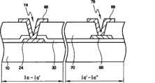
图1A是根据本发明示例性实施例的LCD的薄膜晶体管(TFT)基底的版图,图1B是沿着图1A中的线Ib-Ib′截取的剖视图,图1C是沿着图1A中的线Ic-Ic′和Ic′-Ic″截取的剖视图;1A is a layout of a thin film transistor (TFT) substrate of an LCD according to an exemplary embodiment of the present invention, FIG. 1B is a cross-sectional view taken along the line Ib-Ib' in FIG. 1A , and FIG. 1C is a cross-sectional view taken along the line in FIG. 1A Sectional views taken from Ic-Ic' and Ic'-Ic";
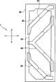
图2是根据本发明示例性实施例的LCD的共电极基底的版图;2 is a layout of a common electrode substrate of an LCD according to an exemplary embodiment of the present invention;
图3A是包括图1A中的TFT基底和图2中的共电极基底的版图,图3B是沿着图3A中的线IIIb-IIIb′截取的剖视图;3A is a layout including the TFT substrate in FIG. 1A and the common electrode substrate in FIG. 2, and FIG. 3B is a cross-sectional view taken along line IIIb-IIIb' in FIG. 3A;
图4是根据本发明示例性实施例的LCD的电路图;4 is a circuit diagram of an LCD according to an exemplary embodiment of the present invention;
图5A是根据本发明另一示例性实施例的LCD的TFT基底的版图,图5B是根据本发明示例性实施例的包括图5A中的TFT基底的LCD的版图。5A is a layout of a TFT substrate of an LCD according to another exemplary embodiment of the present invention, and FIG. 5B is a layout of an LCD including the TFT substrate of FIG. 5A according to an exemplary embodiment of the present invention.
具体实施方式 Detailed ways
通过参照下面对示例性实施例和附图的详细描述,本发明的优点和特征及实现其的方法可更易于理解。然而,本发明可以以多种不同的方式实施,不应理解为限于这里阐述的实施例。提供这些实施例以使本公开是透彻的和完全的,并将本发明的原理完全传达给本领域技术人员,本发明只由权利要求限定。整个说明书中,相同的标号表示相同的元件。Advantages and features of the present invention and a method of achieving the same may be better understood by referring to the following detailed description of exemplary embodiments and accompanying drawings. However, this invention may be embodied in many different ways and should not be construed as limited to the embodiments set forth herein. Rather, these embodiments are provided so that this disclosure will be thorough and complete, and will fully convey the principles of the invention to those skilled in the art, and the present invention is limited only by the claims. Throughout the specification, the same reference numerals refer to the same elements.
应该理解,当元件诸如层、膜、区域或基底称为“在”另一元件“上”时,这个元件可以直接在另一元件上,或者也可存在中间元件。相反,当元件称为“直接”在另一元件“上”时,不存在中间元件。It will be understood that when an element such as a layer, film, region, or substrate is referred to as being "on" another element, it can be directly on the other element or intervening elements may also be present. In contrast, when an element is referred to as being "directly on" another element, there are no intervening elements present.
现在,将参照附图更加全面地描述根据本发明示例性实施例的LCD。Now, an LCD according to an exemplary embodiment of the present invention will be described more fully with reference to the accompanying drawings.
LCD包括:TFT基底,包括由栅极线和数据线限定的像素和TFT;共电极基底,面对TFT基底并包括滤色器。液晶层置于TFT基底和共电极基底之间。液晶层包括其长轴基本上垂直于TFT基底和共电极基底取向的液晶分子。The LCD includes: a TFT substrate including pixels and TFTs defined by gate lines and data lines; a common electrode substrate facing the TFT substrate and including color filters. The liquid crystal layer is placed between the TFT substrate and the common electrode substrate. The liquid crystal layer includes liquid crystal molecules whose long axes are aligned substantially perpendicular to the TFT substrate and the common electrode substrate.
首先,现在将参照图1A、图1B和图1C来更加详细地描述TFT基底。First, a TFT substrate will now be described in more detail with reference to FIGS. 1A , 1B, and 1C.
图1A是根据本发明示例性实施例的LCD的薄膜晶体管(TFT)基底的版图,图1B是沿着图1A中的线Ib-Ib′截取的剖视图,图1C是沿着图1A中的线Ic-Ic′和Ic′-Ic″截取的剖视图。1A is a layout of a thin film transistor (TFT) substrate of an LCD according to an exemplary embodiment of the present invention, FIG. 1B is a cross-sectional view taken along the line Ib-Ib' in FIG. 1A , and FIG. 1C is a cross-sectional view taken along the line in FIG. 1A Sectional views taken from Ic-Ic' and Ic'-Ic".
参照图1A、图1B和图1C,栅极线22沿着水平方向形成在绝缘基底10上,栅电极26从栅极线22突出地形成。从另一层或外部电路接收栅极信号的栅极线端部24形成在栅极线22的一端。为了有效地将栅极线22与外部电路结合,栅极线端部24比栅极线22宽。栅极线22、栅电极26和栅极线端部24构成栅极布线。Referring to FIGS. 1A , 1B and 1C,
此外,存储电极线28沿着水平方向形成在绝缘基底10上,并基本上平行于栅极线22。多个存储电极29a、29b、29c和29d沿着第一子像素电极82a和第二子像素电极82b的边缘形成为存储电极线28的分支。例如,存储电极包括:存储电极垂直图案29a和29b,沿着数据线62从存储电极线28延伸,并与第一子像素电极82a和第二子像素电极82b叠置;存储电极倾斜图案29c和29d,沿着第一子像素电极82a和第二子像素电极82b之间相应的间隙83形成。存储电极倾斜图案29c和29d连接存储电极垂直图案29a和29b。存储电极垂直图案29a和29b可通过使用从存储电极垂直图案29a延伸的存储电极延伸部分27与第一子像素电极82a和第二子像素电极82b叠置。存储电极线28和存储电极29a、29b、29c、29d以及存储电极延伸部分27构成存储电极布线。In addition,
在本实施例中,为了增大LCD的开口率,存储电极布线27、28、29a、29b、29c和29d沿着第一子像素电极82a和第二子像素电极82b的边布置。然而,存储电极布线27、28、29a、29b、29c和29d可具有各种形状和布局,只要满足与第一子像素电极82a和第二子像素电极82b相关的预定存储电容形成条件。In this embodiment, in order to increase the aperture ratio of the LCD, the
栅极布线22、24、26和存储电极布线27、28、29a、29b、29c、29d可由Al、Al合金、Ag、Ag合金、Cu、Cu合金、Mo、Mo合金、Cr、Ti或Ta制成。此外,栅极布线22、24、26和存储电极布线27、28、29a、29b、29c、29d可具有多层结构,该多层结构包括具有不同物理特性的两个导电膜(未示出)。所述两个膜之一可由低阻金属制成,以减小信号延迟或电压降,所述低阻金属包括Al、Al合金、Ag、Ag合金、Cu和Cu合金。另一膜可由具有良好的物理特性、化学特性以及具有与其它材料诸如氧化铟锡(ITO)或氧化铟锌(IZO)的良好的电接触特性的材料诸如Mo、Mo合金、Cr、Ta或Ti制成。所述多层结构的示例包括下Cr膜和上Al膜,以及下Al膜和上Mo膜。然而,栅极布线22、24、26和存储电极布线27、28、29a、29b、29c、29d可由各种金属或导体制成。
栅极绝缘层30形成在栅极布线22、24、26和存储电极布线27、28、29a、29b、29c、29d上。
可由氢化非晶硅或多孔硅形成的半导体层40形成在栅极绝缘层30上。半导体层40可具有各种形状如岛状或线状。例如,图1A示出了岛状的半导体层40。当半导体层40为线状时,它可位于数据线62的下面并延伸到栅电极26。A
欧姆接触层55和56可由例如硅化物或以高浓度n型杂质掺杂的n+氢化硅形成在半导体层40上。欧姆接触层55和56可具有各种形状如岛状或线状。例如,图1B示出了位于漏电极66和源电极65的下面的岛状的欧姆接触层55和56。线状的欧姆接触层可在栅电极26的上面延伸。The ohmic contact layers 55 and 56 may be formed on the
数据线62和漏电极66形成在欧姆接触层55、56和栅极绝缘层30上。数据线62在纵向上延伸,以与栅极线22交叉,从而限定像素。源电极65从数据线62分支并在半导体层40的上面延伸。从另一层或从外部电路接收数据信号并将数据信号传输到数据线62的数据线端部68形成在数据线62的一端。为了有效地将数据线62与外部电路结合,数据线端部68比数据线62宽。漏电极66和源电极65彼此分开,并位于栅电极26的相对侧。A
漏电极66包括形成在半导体层40上的条型图案和从条形图案延伸并通过接触孔76部分地暴露的漏电极延伸部分67。以与漏电极66相同的材料形成并与漏电极66形成在相同的层上的耦合电极69从漏电极66分支。耦合电极69与第二子像素电极82b叠置,从而与第二子像素电极82b形成耦合电容。为了提高开口率并防止纹理和光泄漏,耦合电极69可沿着共电极的切口(图2和图3A的92)形成。数据线62、数据线端部68、源电极65、包括漏电极延伸部分67的漏电极66、耦合电极69构成数据布线。The
数据布线62、65、66、67、68和69可由难熔金属如Cr、Mo、Ti、Ta或它们的合金制成。另外,数据布线62、65、66、67、68和69可具有包括低阻膜(未示出)和优良接触膜(未示出)的多层结构。该多层结构的示例包括下Cr膜和上Al膜的双层结构、下Al膜和上Mo膜的双层结构以及下Mo膜、中Al膜和上Mo膜的三层结构。The data wirings 62, 65, 66, 67, 68 and 69 may be made of refractory metals such as Cr, Mo, Ti, Ta or their alloys. In addition, the data wirings 62, 65, 66, 67, 68, and 69 may have a multilayer structure including a low resistance film (not shown) and a good contact film (not shown). Examples of the multilayer structure include a double-layer structure of a lower Cr film and an upper Al film, a double-layer structure of a lower Al film and an upper Mo film, and a three-layer structure of a lower Mo film, a middle Al film, and an upper Mo film.
源电极65与半导体层40至少部分地叠置,漏电极66和源电极65至少部分覆盖半导体层40地位于栅电极26的相对侧。这里,欧姆接触55置于半导体层40和源电极65之间,欧姆接触56置于半导体层40和漏电极66之间,以减小半导体层40和源电极65之间以及半导体层40和漏电极66之间的接触电阻。The source electrode 65 at least partially overlaps the
用作绝缘层的钝化层70形成在数据线62、漏电极66和半导体层40上。这里,钝化(保护)层70可由通过等离子体增强化学气相沉积(PECVD)形成的低介电绝缘材料如a-Si:C:O和a-Si:O:F、具有良好平坦性的光敏有机材料或者无机绝缘体如氮化硅或二氧化硅制成。可选择地,为了在保持有机层特性的同时保护暴露的半导体层40,钝化层70可具有下无机膜和上有机膜的双层结构。A
穿过钝化层70形成接触孔76和接触孔78,以分别暴露漏电极66和数据线端部68。穿过钝化层70和栅极绝缘层30形成接触孔74,以暴露栅极线端部24。A
像素电极82与像素的形状相对应地形成在钝化层70上。像素电极82包括被间隙83分开的第一子像素电极82a和第二子像素电极82b。间隙与偏振片的透射轴1形成大约45度或-45度的角度。第二子像素电极82b形成旋转的‘V’形,并位于像素区域的中间。第一子像素电极82a形成在像素区域没有第二子像素电极82b的部分上。这里,多个切口(未示出)可沿着倾斜的方向形成在第一子像素电极82a和第二子像素电极82b中,或者多个突出(未示出)可沿着倾斜的方向形成在第一子像素电极82a和第二子像素电极82b上。考虑到当向液晶层施加电场时液晶分子的指向矢的方向,可将像素电极82的显示区域划分成多个畴。使用形成在像素电极82中的切口或形成在像素电极82上的突出,每个畴可被划分成多个子畴。The
第一子像素电极82a通过接触孔76电连接到漏电极66,通过从漏电极66延伸的耦合电极69,第二子像素电极82b耦合到漏电极66,但不直接与漏电极66连接。The
辅助栅极线端部86和辅助数据线端部88形成在钝化层70上,并通过接触孔74与栅极线端部24连接,通过接触孔78与数据线端部68连接。此外,穿过钝化层70形成接触孔77,以暴露存储电极布线27、28、29a、29b、29c和29d。连接元件84形成在钝化层70上,并电连接相邻的像素区域的存储电极布线27、28、29a、29b、29c和29d。这里,第一子像素电极82a、第二子像素电极82b和辅助栅极线端部86、辅助数据线端部88可由透明导体如ITO、IZO或反射型导体如Al制成。辅助栅极线端部86将栅极线端部24与外部器件电连接,辅助数据线端部88将数据线端部68与外部器件电连接。The auxiliary
第一子像素电极82a通过接触孔76物理连接且电连接到漏电极66,漏电极66向第一子像素电极82a施加数据电压。第二子像素电极82b电浮置,并通过与漏电极66连接且与第二子像素电极82b叠置的耦合电极69与第一子像素电极82a容性耦合。The
换句话讲,第二子像素电极82b的电压根据第一子像素电极82a的电压而改变。第二子像素电极82b的电压的绝对值可总小于第一子像素电极82a的电压的绝对值。可选择地,数据电压可施加到第二子像素电极82b,第一子像素电极82a可与第二子像素电极82b容性耦合。In other words, the voltage of the
当如上所述地布置像素时,可补偿具有不同数据电压的第一子像素电极82a和第二子像素电极82b,因而减小了伽马曲线扭曲并加宽了参考视角。When the pixels are arranged as described above, the
如上所述,即使当在存储电极布线27、28、29a、29b、29c、29d之上形成像素电极82时出现叠置误差,也可基本上均匀地保持像素电极82和存储电极布线27、28、29a、29b、29c、29d之间的叠置面积,从而基本上均匀地保持多个相邻畴之间的电压比。例如,像素电极82被形成为它的两边都可叠加在存储电极垂直图案29a和29b上。因此,即使当在存储电极布线27、28、29a、29b、29c、29d之上形成像素电极82时出现叠置误差,也由于可以补偿像素电极82和存储电极垂直图案29a、29b的叠置面积而可以基本上均匀地保持像素电极82和存储电极布线27、28、29a、29b、29c、29d之间的叠置面积。当通过耦合电极69将第二子像素电极82b与第一子像素电极82a容性耦合时,第二子像素电极82b可被形成为它的右侧部分与存储电极垂直图案29b叠置,而它的左侧部分与从存储电极垂直图案29a延伸并比存储电极垂直图案29a宽的存储电极延伸部分27叠置。这里,下面将参照图4来详细描述第一子像素电极82a和第二子像素电极82b的耦合。As described above, even if an overlay error occurs when the
用于使液晶层取向的取向层(未示出)可形成在像素电极82、辅助栅极线端部86、辅助数据线端部88和钝化层70上。An alignment layer (not shown) for aligning the liquid crystal layer may be formed on the
现在将参照图2、图3A和图3B来详细描述根据本发明示例性实施例的LCD的共电极基底和具有该共电极基底的LCD。图2是根据本发明示例性实施例的LCD的共电极基底的版图,图3A是图1A中的TFT基底和图2中的共电极基底的版图,图3B是沿着图3A中的线IIIb-IIIb′截取的剖视图。A common electrode substrate of an LCD according to an exemplary embodiment of the present invention and an LCD having the same will now be described in detail with reference to FIGS. 2 , 3A, and 3B. 2 is a layout of a common electrode substrate of an LCD according to an exemplary embodiment of the present invention, FIG. 3A is a layout of a TFT substrate in FIG. 1A and a common electrode substrate in FIG. 2 , and FIG. 3B is along line IIIb in FIG. 3A - Sectional view taken from IIIb'.
参照图2、图3A和图3B,顺序布置在各像素中的滤色器98(例如,红色、绿色和蓝色滤色器)和防止光泄漏的黑色矩阵94形成在可为透明绝缘材料如玻璃的绝缘材料96上。共电极90由透明导电材料如ITO或IZO形成在滤色器98上,共电极90包括倾斜的切口92。每个倾斜的切口92在中间具有凹口91。凹口91可为三角形、矩形、梯形或半圆形。畴边界附近的液晶分子由于凹口91而可为稳定且均匀地排列,因此防止了在畴边界附近产生暗点或余像。Referring to FIGS. 2, 3A and 3B, color filters 98 (for example, red, green and blue color filters) sequentially arranged in each pixel and a
共电极90面对像素电极82,并包括与偏振片2的透射轴1形成大约45度或-45度的角度的倾斜切口92。共电极90可包括代替倾斜切口92的突出(未示出)。倾斜的切口92和突出可称为畴划分件。The
用于使液晶分子取向的取向层(未示出)可形成在共电极90上。An alignment layer (not shown) for aligning liquid crystal molecules may be formed on the
参照图3A,共电极90的倾斜切口92以及使第一子像素电极82a和第二子像素电极82b分开的间隙83可交替地布置。Referring to FIG. 3A ,
参照图3B,TFT基底100和共电极基底200彼此垂直地排列,液晶层300置于其间且彼此耦合,因而形成根据本发明示例性实施例的LCD的基本结构。Referring to FIG. 3B , the
包括在液晶层300中的液晶分子取向为它们的指向矢可垂直于TFT基底100和共电极基底200,并具有负的介电各向异性。TFT基底100和共电极基底200彼此排列成使得像素电极82和滤色器98彼此精确叠置。然后,像素可被倾斜的切口92和间隙83划分成多个畴。根据液晶分子取向的方向,像素可被间隙83划分成左畴和右畴,也可被划分成上畴和下畴。换句话讲,根据当电场施加到液晶层时包括在液晶层中的液晶分子的指向矢的方向,像素可被划分成多个畴。Liquid crystal molecules included in the liquid crystal layer 300 are aligned such that their directors may be perpendicular to the
根据本发明示例性实施例的LCD不仅可包括在图3B中示出的基本结构,而且也可包括其它的元件,如偏振片和背光组件。An LCD according to an exemplary embodiment of the present invention may include not only the basic structure shown in FIG. 3B but also other elements such as a polarizing plate and a backlight assembly.
偏振片2可以以这样的方式安装在基本结构的一侧上,即,一个透射轴平行于栅极线22,另一透射轴垂直于栅极线22。The
在根据本发明示例性实施例的LCD中,当对像素的多个畴的每个中的液晶施加电场时,上述液晶垂直于间隙83或倾斜的切口92倾斜。因此,在每个畴中的液晶与偏振片2的透射轴形成大约45度或-45度的角度。形成在各间隙83或倾斜的切口92中的侧向电场有助于在各个畴中的液晶取向。In the LCD according to the exemplary embodiment of the present invention, when an electric field is applied to the liquid crystal in each of the plurality of domains of the pixel, the liquid crystal is inclined vertically to the
在这个LCD中,图像信号电压可被从TFT施加到第一子像素电极82a,第二子像素电极82b与第一子像素电极82a容性耦合。因此,第二子像素电极82b的电压根据施加到第一子像素电极82a的图像信号电压而改变。此外,第二子像素电极82b的电压的绝对值将小于第一子像素电极82a的电压的绝对值。因此,如上所述,通过以这样的方式在像素中布置第一子像素电极82a和第二子像素电极82b,使得它们可彼此互补,可减小伽马曲线扭曲的可能性。In this LCD, an image signal voltage may be applied from the TFT to the
现在将参照图4来详细描述第一子像素电极82a和第二子像素电极82b的耦合,图4是根据本发明示例性实施例的LCD的电路图。The coupling of the
参照图3A和图4,Clca是形成在第一子像素电极82a和共电极90之间的液晶电容器,Csta是形成在第一子像素电极82a和存储电极布线27、28、29a、29b、29c、29d之间的存储电容器,Cstb是形成在第二子像素电极82b和存储电极布线27、28、29a、29b、29c、29d之间的存储电容器,Clcb是形成在第二子像素电极82b和共电极90之间的液晶电容器,Ccp是形成在第一子像素电极82a和第二子像素电极82b之间特别是形成在第二子像素电极82b和耦合电极69之间的耦合电容器。Referring to FIG. 3A and FIG. 4, Clca is a liquid crystal capacitor formed between the first
参照图4,像素的TFT Q是包括控制端部(例如,栅电极26)、输入端部(例如,源电极65)和输出端部(例如,漏电极66)的三端部器件,其中,控制端部与栅极线G(例如,栅极线22)电连接,输入端部与数据线D(例如,数据线62)电连接,输出端部与液晶电容器Clca、Clcb以及存储电容器Cst电连接。Referring to FIG. 4, the TFT Q of the pixel is a three-terminal device including a control terminal (for example, gate electrode 26), an input terminal (for example, source electrode 65) and an output terminal (for example, drain electrode 66), wherein, The control terminal is electrically connected to the gate line G (for example, the gate line 22), the input terminal is electrically connected to the data line D (for example, the data line 62), and the output terminal is connected to the liquid crystal capacitorsClca ,Clcb and the storage capacitor Cst electrical connection.
第一子像素电极82a和第二子像素电极82b的电压分别以Va和Vb表示。电压分布规律为:The voltages of the
Vb=Va×[Ccp/(Ccp+Clcb+Cstb)]Vb=Va×[Ccp /(Ccp +Clcb +Cstb )]
由于Ccp/(Ccp+Clcb+Cstb)总小于1,所以电压Vb将小于电压Va。通过控制电容器Ccp的电容,可调节Vb对Va的比,通过调节第二子像素电极82b与耦合电极69之间的接触面积或距离可控制电容器Ccp的电容。如上所述,可以以各种方式布置耦合电极69。Since Ccp /(Ccp +Clcb +Cstb ) is always less than 1, the voltage Vb will be less than the voltage Va. The ratio of Vb to Va can be adjusted by controlling the capacitance of the capacitor Ccp , and the capacitance of the capacitor Ccp can be controlled by adjusting the contact area or distance between the
这里,如果当在存储电极布线27、28、29a、29b、29c、29d之上形成像素电极82时出现叠置误差,则电容器Cstb的电容可根据第二子像素电极82b与存储电极布线27、28、29a、29b、29c、29d之间的叠置面积而改变。因此,为了基本上均匀地保持电压Va与电压Vb之比,包括电容器Cstb的LCD应该被设计成不管当在存储电极布线27、28、29a、29b、29c、29d之上形成像素电极82时是否出现叠置误差,电容器Cstb都具有预定的电容。Here, if an overlay error occurs when the
如上所述,在根据本发明示例性实施例的LCD中,以这样的方式形成第二子像素电极82b,即,它的右侧部分与存储电极垂直图案29b叠置,它的左侧部分与从存储电极垂直图案29a延伸的存储电极延伸部分27叠置。因此,即使当在存储电极布线27、28、29a、29b、29c、29d之上形成像素电极82时出现叠置误差,也可基本上均匀地保持电容器Cstb的电容。结果,可基本上均匀地保持电压Va和电压Vb之比,从而防止LCD的显示特性劣化。As described above, in the LCD according to the exemplary embodiment of the present invention, the
现在,将参照图5A和图5B来详细描述根据本发明另一示例性实施例的LCD。Now, an LCD according to another exemplary embodiment of the present invention will be described in detail with reference to FIGS. 5A and 5B.
图5A是LCD的TFT基底的版图,图5B是根据本发明示例性实施例的包括图5A中的TFT基底的LCD的版图。如图5A和图5B所示,相同的元件分别以相同的标号表示,省略对它们的重复描述。5A is a layout of a TFT substrate of an LCD, and FIG. 5B is a layout of an LCD including the TFT substrate of FIG. 5A according to an exemplary embodiment of the present invention. As shown in FIG. 5A and FIG. 5B , the same components are denoted by the same reference numerals, and their repeated descriptions are omitted.
参照图5A和图5B,修改了第二子像素电极582b,使得第二子像素电极582b和存储电极延伸部分27的叠置面积与第二子像素电极582b和存储电极垂直图案29b的叠置面积基本上相同。凹进A形成在第二子像素电极582b的右侧上(即,形成在第二子像素电极582b的最长的侧边上),使得第二子像素电极582b和存储电极垂直图案29b的叠置面积与第二子像素电极582b和存储电极延伸部分27的叠置面积基本上相同。5A and 5B, the
因此,即使当在存储电极布线27、28、29a、29b、29c、29d之上形成像素电极58,具体地讲,当在存储电极布线27、28、29a、29b、29c、29d之上形成第二子像素电极582b时出现叠置误差,也可基本上均匀地保持第二子像素电极582b和存储电极布线27、28、29a、29b、29c、29d的叠置面积。因此,可基本上均匀地保持施加到第一子像素电极82a的电压对施加到第二子像素电极582b的电压之比,从而改进了LCD的显示特性。Therefore, even when the pixel electrode 58 is formed over the
如上所述,即使当在存储电极布线之上形成像素电极时出现叠置误差,根据本发明示例性实施例的LCD也可基本上均匀地保持像素电极和存储电极布线的叠置面积,从而改进了LCD的显示特性。As described above, even if an overlay error occurs when a pixel electrode is formed over a storage electrode wiring, the LCD according to an exemplary embodiment of the present invention can maintain the overlapping area of the pixel electrode and the storage electrode wiring substantially uniformly, thereby improving LCD display characteristics.
本领域技术人员将清楚,在不脱离本发明的精神或范围的情况下,可对本发明作出各种修改和变化。因此,本发明意在覆盖本发明的修改和变化,只要它们落入权利要求及其等同物的范围。It will be apparent to those skilled in the art that various modifications and variations can be made in the present invention without departing from the spirit or scope of the inventions. Thus, it is intended that the present invention cover the modifications and variations of this invention provided they come within the scope of the claims and their equivalents.
Claims (6)
Translated fromChineseApplications Claiming Priority (3)
| Application Number | Priority Date | Filing Date | Title |
|---|---|---|---|
| KR10-2005-0070695 | 2005-08-02 | ||
| KR1020050070695AKR101237011B1 (en) | 2005-08-02 | 2005-08-02 | Liquid crystal display |
| KR1020050070695 | 2005-08-02 |
Publications (2)
| Publication Number | Publication Date |
|---|---|
| CN1908789A CN1908789A (en) | 2007-02-07 |
| CN1908789Btrue CN1908789B (en) | 2010-07-28 |
Family
ID=37699929
Family Applications (1)
| Application Number | Title | Priority Date | Filing Date |
|---|---|---|---|
| CN2006101083647AExpired - Fee RelatedCN1908789B (en) | 2005-08-02 | 2006-08-02 | Liquid crystal display device |
Country Status (3)
| Country | Link |
|---|---|
| US (1) | US7440040B2 (en) |
| KR (1) | KR101237011B1 (en) |
| CN (1) | CN1908789B (en) |
Families Citing this family (21)
| Publication number | Priority date | Publication date | Assignee | Title |
|---|---|---|---|---|
| KR101189267B1 (en)* | 2004-12-03 | 2012-10-09 | 삼성디스플레이 주식회사 | A thin film transistor array panel and a liquid crystal display |
| US8901268B2 (en)* | 2004-08-03 | 2014-12-02 | Ahila Krishnamoorthy | Compositions, layers and films for optoelectronic devices, methods of production and uses thereof |
| KR101090253B1 (en)* | 2004-10-06 | 2011-12-06 | 삼성전자주식회사 | Thin film transistor array panel and liquid crystal display including the same |
| KR20080000202A (en)* | 2006-06-27 | 2008-01-02 | 삼성전자주식회사 | Display board and display panel having same |
| KR101309552B1 (en)* | 2006-11-01 | 2013-09-23 | 삼성디스플레이 주식회사 | Array substrate and display panel having the same |
| KR101309777B1 (en)* | 2007-01-03 | 2013-09-25 | 삼성디스플레이 주식회사 | Thin film transistor substrate and display device having the same |
| TWI372929B (en)* | 2007-03-30 | 2012-09-21 | Chunghwa Picture Tubes Ltd | Pixel structure and driving method |
| KR101382480B1 (en)* | 2007-09-12 | 2014-04-09 | 삼성디스플레이 주식회사 | Liquid crystal display |
| KR101392741B1 (en)* | 2007-10-29 | 2014-05-09 | 삼성디스플레이 주식회사 | Display substrate and display panel having the same |
| KR101375831B1 (en)* | 2007-12-03 | 2014-04-02 | 삼성전자주식회사 | Display device using oxide semiconductor thin film transistor |
| KR101502836B1 (en)* | 2008-03-21 | 2015-03-16 | 삼성디스플레이 주식회사 | Liquid crystal display panel |
| KR101549962B1 (en)* | 2008-11-28 | 2015-09-04 | 삼성디스플레이 주식회사 | Liquid crystal display |
| KR101641982B1 (en)* | 2009-02-09 | 2016-07-25 | 삼성디스플레이 주식회사 | Display device |
| KR101626029B1 (en)* | 2009-02-18 | 2016-06-01 | 삼성디스플레이 주식회사 | Thin film transistor panel |
| CN101881911B (en)* | 2009-05-07 | 2012-08-22 | 上海天马微电子有限公司 | Liquid crystal display device and driving method thereof |
| US8557877B2 (en) | 2009-06-10 | 2013-10-15 | Honeywell International Inc. | Anti-reflective coatings for optically transparent substrates |
| KR101101007B1 (en) | 2009-10-09 | 2011-12-29 | 삼성모바일디스플레이주식회사 | LCD Display |
| KR101101021B1 (en) | 2009-10-09 | 2011-12-29 | 삼성모바일디스플레이주식회사 | Liquid crystal display device and manufacturing method thereof |
| US8864898B2 (en) | 2011-05-31 | 2014-10-21 | Honeywell International Inc. | Coating formulations for optical elements |
| TWI515493B (en)* | 2013-07-19 | 2016-01-01 | 友達光電股份有限公司 | Pixel structure |
| JP6803842B2 (en) | 2015-04-13 | 2020-12-23 | ハネウェル・インターナショナル・インコーポレーテッドHoneywell International Inc. | Polysiloxane formulations and coatings for optoelectronic applications |
Citations (2)
| Publication number | Priority date | Publication date | Assignee | Title |
|---|---|---|---|---|
| US5159476A (en)* | 1988-12-28 | 1992-10-27 | Sony Corporation | Liquid crystal display unit having large image area and high resolution |
| US6040882A (en)* | 1996-10-16 | 2000-03-21 | Hyundai Electronics Industries Co., Ltd. | Liquid crystal display device having "H" character common electrode and method of fabricating thereof |
Family Cites Families (4)
| Publication number | Priority date | Publication date | Assignee | Title |
|---|---|---|---|---|
| KR100925459B1 (en)* | 2002-12-24 | 2009-11-06 | 삼성전자주식회사 | Multi-domain liquid crystal display and display panel used therefor |
| KR100984346B1 (en)* | 2003-05-19 | 2010-09-30 | 삼성전자주식회사 | Multi-domain liquid crystal display and display panel used therefor |
| KR20040105934A (en)* | 2003-06-10 | 2004-12-17 | 삼성전자주식회사 | Liquid crystal display having multi domain and panel for the same |
| US7206048B2 (en)* | 2003-08-13 | 2007-04-17 | Samsung Electronics Co., Ltd. | Liquid crystal display and panel therefor |
- 2005
- 2005-08-02KRKR1020050070695Apatent/KR101237011B1/ennot_activeExpired - Fee Related
- 2006
- 2006-07-27USUS11/460,380patent/US7440040B2/enactiveActive
- 2006-08-02CNCN2006101083647Apatent/CN1908789B/ennot_activeExpired - Fee Related
Patent Citations (2)
| Publication number | Priority date | Publication date | Assignee | Title |
|---|---|---|---|---|
| US5159476A (en)* | 1988-12-28 | 1992-10-27 | Sony Corporation | Liquid crystal display unit having large image area and high resolution |
| US6040882A (en)* | 1996-10-16 | 2000-03-21 | Hyundai Electronics Industries Co., Ltd. | Liquid crystal display device having "H" character common electrode and method of fabricating thereof |
Also Published As
| Publication number | Publication date |
|---|---|
| US7440040B2 (en) | 2008-10-21 |
| US20070030407A1 (en) | 2007-02-08 |
| CN1908789A (en) | 2007-02-07 |
| KR101237011B1 (en) | 2013-02-26 |
| KR20070015982A (en) | 2007-02-07 |
Similar Documents
| Publication | Publication Date | Title |
|---|---|---|
| CN1908789B (en) | Liquid crystal display device | |
| US7113233B2 (en) | Thin film transistor array panel with varying coupling capacitance between first and second pixel electrodes | |
| US8564745B2 (en) | Liquid crystal display having more than one color portion within a pixel | |
| JP4953416B2 (en) | Liquid crystal display | |
| US7777823B2 (en) | Thin film transistor array panel | |
| US7443458B2 (en) | Liquid crystal display with wide viewing angle | |
| US20070182872A1 (en) | Multi-domain liquid crystal display and a thin film transistor substrate of the same | |
| US20150022766A1 (en) | Liquid crystal display | |
| US6762815B2 (en) | In-plane switching LCD with a redundancy structure for an opened common electrode and a high storage capacitance | |
| US7773165B2 (en) | Liquid crystal display | |
| KR101247698B1 (en) | Liquid crystal display | |
| US7486343B2 (en) | TFT array panel having a two-portion coupling electrode extending from drain electrode in different directions with first portion extending along a gap between two overlapping subpixel electrodes thereon and second portion extending in same direction as data line | |
| US7782415B2 (en) | Active matrix subtrate, liquid crystal display panel and method of manufacturing the same | |
| US7929099B2 (en) | Liquid crystal display with improved lateral visibility | |
| US20090114920A1 (en) | Tft substrate and liquid cyrstal display device having the same | |
| US6864935B2 (en) | Liquid crystal display | |
| US7220992B2 (en) | Thin film transistor array panel and a liquid crystal display including the same | |
| KR101133757B1 (en) | Liquid crystal display | |
| KR101297737B1 (en) | Liquid crystal display | |
| KR20050076402A (en) | Liquid crystal display and thin film transistor array panel therefor | |
| KR20060020893A (en) | Multi Domain Thin Film Transistor Display Panel | |
| KR101230317B1 (en) | Liquid crystal display | |
| KR20070038332A (en) | Liquid crystal display | |
| KR20070026910A (en) | Liquid crystal display | |
| KR20070037146A (en) | Display panel and liquid crystal display including the same |
Legal Events
| Date | Code | Title | Description |
|---|---|---|---|
| C06 | Publication | ||
| PB01 | Publication | ||
| C10 | Entry into substantive examination | ||
| SE01 | Entry into force of request for substantive examination | ||
| C14 | Grant of patent or utility model | ||
| GR01 | Patent grant | ||
| ASS | Succession or assignment of patent right | Owner name:SAMSUNG DISPLAY CO., LTD. Free format text:FORMER OWNER: SAMSUNG ELECTRONICS CO., LTD. Effective date:20121220 | |
| C41 | Transfer of patent application or patent right or utility model | ||
| TR01 | Transfer of patent right | Effective date of registration:20121220 Address after:South Korea Gyeonggi Do Yongin Patentee after:Samsung Display Co.,Ltd. Address before:Gyeonggi Do Lingtong District South Korea Suwon Mei Tan 3 hole 416 Patentee before:Samsung Electronics Co.,Ltd. | |
| CF01 | Termination of patent right due to non-payment of annual fee | Granted publication date:20100728 Termination date:20200802 | |
| CF01 | Termination of patent right due to non-payment of annual fee |