CN1905789B - Electromagnetic wave absorbing thin film structure and manufacturing method thereof - Google Patents
Electromagnetic wave absorbing thin film structure and manufacturing method thereofDownload PDFInfo
- Publication number
- CN1905789B CN1905789BCN2005100855250ACN200510085525ACN1905789BCN 1905789 BCN1905789 BCN 1905789BCN 2005100855250 ACN2005100855250 ACN 2005100855250ACN 200510085525 ACN200510085525 ACN 200510085525ACN 1905789 BCN1905789 BCN 1905789B
- Authority
- CN
- China
- Prior art keywords
- layer
- electromagnetic wave
- film structure
- composite bed
- particles
- Prior art date
- Legal status (The legal status is an assumption and is not a legal conclusion. Google has not performed a legal analysis and makes no representation as to the accuracy of the status listed.)
- Expired - Fee Related
Links
- 238000004519manufacturing processMethods0.000titleclaimsabstractdescription15
- 239000010409thin filmSubstances0.000titledescription7
- 239000002245particleSubstances0.000claimsabstractdescription52
- 239000002131composite materialSubstances0.000claimsabstractdescription35
- 238000010521absorption reactionMethods0.000claimsabstractdescription15
- 239000000463materialSubstances0.000claimsdescription15
- 238000000034methodMethods0.000claimsdescription13
- 229920000642polymerPolymers0.000claimsdescription12
- 229910052751metalInorganic materials0.000claimsdescription5
- 239000002184metalSubstances0.000claimsdescription5
- 239000011358absorbing materialSubstances0.000claimsdescription4
- 238000000465mouldingMethods0.000claimsdescription4
- 229920006254polymer filmPolymers0.000claimsdescription4
- 229920002521macromoleculePolymers0.000claims3
- 230000004888barrier functionEffects0.000claims1
- 230000001413cellular effectEffects0.000claims1
- 150000001875compoundsChemical class0.000claims1
- 239000010410layerSubstances0.000abstractdescription84
- 239000002356single layerSubstances0.000abstractdescription7
- 230000001066destructive effectEffects0.000abstractdescription5
- 230000006378damageEffects0.000abstractdescription3
- 239000010408filmSubstances0.000description16
- 238000010586diagramMethods0.000description7
- 230000000694effectsEffects0.000description5
- 230000008569processEffects0.000description5
- XEEYBQQBJWHFJM-UHFFFAOYSA-NIronChemical compound[Fe]XEEYBQQBJWHFJM-UHFFFAOYSA-N0.000description4
- PXHVJJICTQNCMI-UHFFFAOYSA-NNickelChemical compound[Ni]PXHVJJICTQNCMI-UHFFFAOYSA-N0.000description4
- 229910045601alloyInorganic materials0.000description3
- 239000000956alloySubstances0.000description3
- 239000000919ceramicSubstances0.000description3
- 230000004048modificationEffects0.000description3
- 238000012986modificationMethods0.000description3
- RYGMFSIKBFXOCR-UHFFFAOYSA-NCopperChemical compound[Cu]RYGMFSIKBFXOCR-UHFFFAOYSA-N0.000description2
- 239000012790adhesive layerSubstances0.000description2
- 229910052782aluminiumInorganic materials0.000description2
- XAGFODPZIPBFFR-UHFFFAOYSA-NaluminiumChemical compound[Al]XAGFODPZIPBFFR-UHFFFAOYSA-N0.000description2
- 239000010941cobaltSubstances0.000description2
- 229910017052cobaltInorganic materials0.000description2
- GUTLYIVDDKVIGB-UHFFFAOYSA-Ncobalt atomChemical compound[Co]GUTLYIVDDKVIGB-UHFFFAOYSA-N0.000description2
- 238000004891communicationMethods0.000description2
- 229910052802copperInorganic materials0.000description2
- 239000010949copperSubstances0.000description2
- 238000005516engineering processMethods0.000description2
- 239000000835fiberSubstances0.000description2
- 230000006870functionEffects0.000description2
- 239000003292glueSubstances0.000description2
- 229910052742ironInorganic materials0.000description2
- 229910052759nickelInorganic materials0.000description2
- 239000004575stoneSubstances0.000description2
- 229940070527tourmalineDrugs0.000description2
- 229910052613tourmalineInorganic materials0.000description2
- 239000011032tourmalineSubstances0.000description2
- 229910000838Al alloyInorganic materials0.000description1
- 208000000044AmnesiaDiseases0.000description1
- 208000003174Brain NeoplasmsDiseases0.000description1
- 230000005778DNA damageEffects0.000description1
- 231100000277DNA damageToxicity0.000description1
- FYYHWMGAXLPEAU-UHFFFAOYSA-NMagnesiumChemical compound[Mg]FYYHWMGAXLPEAU-UHFFFAOYSA-N0.000description1
- PWHULOQIROXLJO-UHFFFAOYSA-NManganeseChemical compound[Mn]PWHULOQIROXLJO-UHFFFAOYSA-N0.000description1
- 208000026139Memory diseaseDiseases0.000description1
- RTAQQCXQSZGOHL-UHFFFAOYSA-NTitaniumChemical compound[Ti]RTAQQCXQSZGOHL-UHFFFAOYSA-N0.000description1
- 230000002745absorbentEffects0.000description1
- 239000002250absorbentSubstances0.000description1
- 238000004026adhesive bondingMethods0.000description1
- 230000002238attenuated effectEffects0.000description1
- 230000003542behavioural effectEffects0.000description1
- 230000015572biosynthetic processEffects0.000description1
- 230000000903blocking effectEffects0.000description1
- 210000004556brainAnatomy0.000description1
- 230000008859changeEffects0.000description1
- 239000011248coating agentSubstances0.000description1
- 238000000576coating methodMethods0.000description1
- 201000010099diseaseDiseases0.000description1
- 208000037265diseases, disorders, signs and symptomsDiseases0.000description1
- 230000005684electric fieldEffects0.000description1
- 238000009713electroplatingMethods0.000description1
- 230000008030eliminationEffects0.000description1
- 238000003379elimination reactionMethods0.000description1
- 238000001125extrusionMethods0.000description1
- 239000004744fabricSubstances0.000description1
- 230000036541healthEffects0.000description1
- 210000005260human cellAnatomy0.000description1
- 238000009413insulationMethods0.000description1
- 238000010030laminatingMethods0.000description1
- 208000032839leukemiaDiseases0.000description1
- 239000011777magnesiumSubstances0.000description1
- 229910052749magnesiumInorganic materials0.000description1
- 229910052748manganeseInorganic materials0.000description1
- 239000011572manganeseSubstances0.000description1
- 230000006984memory degenerationEffects0.000description1
- 208000023060memory lossDiseases0.000description1
- 230000000149penetrating effectEffects0.000description1
- 230000035515penetrationEffects0.000description1
- 239000004033plasticSubstances0.000description1
- 229910052710siliconInorganic materials0.000description1
- 239000010703siliconSubstances0.000description1
- HBMJWWWQQXIZIP-UHFFFAOYSA-Nsilicon carbideChemical compound[Si+]#[C-]HBMJWWWQQXIZIP-UHFFFAOYSA-N0.000description1
- 229910010271silicon carbideInorganic materials0.000description1
- 238000004544sputter depositionMethods0.000description1
- 239000000758substrateSubstances0.000description1
- 239000010936titaniumSubstances0.000description1
- 229910052719titaniumInorganic materials0.000description1
- 239000002023woodSubstances0.000description1
Images


Landscapes
- Shielding Devices Or Components To Electric Or Magnetic Fields (AREA)
Abstract
Description
Translated fromChinese技术领域technical field
本发明系有关于一种防电磁波的材料,特别是关于一种利用波相位相消原理所形成的电磁波吸收薄膜结构及其制造方法。 The invention relates to a material for preventing electromagnetic waves, in particular to an electromagnetic wave absorbing thin film structure and a manufacturing method thereof formed by using the principle of wave phase cancellation. the
背景技术Background technique
随着计算机、通讯、消费性计算机产品功能不断的增加及数字化、高频化、普及化,人体暴露在高能量电磁波的机会越来越多,造成对人体健康的危害,增加了白血病、脑瘤、DNA破坏等患病机率。根据研究指出,当电磁波超过60赫兹,对人体的细胞DNA结构会造成伤害;甚者在一些国外的研究报告中更指出,移动电话会对人的脑部产生如暂时失去记忆、行为能力降低等影响,正因为电磁波的负面影响不断地被发掘,因此,抗电磁波的材料已成为各方的研究重点。 With the continuous increase in the functions of computers, communications, and consumer computer products, as well as digitization, high-frequency, and popularization, the human body is exposed to more and more opportunities for high-energy electromagnetic waves, causing harm to human health and increasing the incidence of leukemia and brain tumors. , DNA damage and other disease probability. According to research, when the electromagnetic wave exceeds 60 Hz, it will cause damage to the DNA structure of human cells; even in some foreign research reports, it has been pointed out that mobile phones can cause temporary memory loss and reduced behavioral ability to the human brain. Just because the negative effects of electromagnetic waves are constantly being discovered, the anti-electromagnetic wave materials have become the research focus of all parties. the
一般抗电磁波材的结构可大略分为电场遮蔽材与磁场遮蔽材两大类。另外目前还有一种采用特殊金属纤维与其它纤维混纺、织造而成的抗EMI功能性织物,或者有的则以有机复合材料,应用高分子渗布处理技术,以外表涂布来改变各种材质包括五金、塑料、镁、钛、铝合金及木材、陶瓷等材料的表面特性来达到抗电磁波的功能。 Generally, the structure of anti-electromagnetic wave materials can be roughly divided into two categories: electric field shielding materials and magnetic field shielding materials. In addition, there is currently a kind of anti-EMI functional fabric that is made of special metal fiber and other fibers blended and woven, or some organic composite materials are used to apply polymer penetration treatment technology to change various materials by surface coating. Including the surface properties of metal, plastic, magnesium, titanium, aluminum alloy, wood, ceramics and other materials to achieve the function of anti-electromagnetic wave. the
然而,公知的各种抗电磁波装置都是厚度大的结构,因而限定其应用范围,尤其是应用越来越讲究轻薄短小的电子产品,例如手机上。而且,公知的抗电磁波装置虽号称其遮蔽效果很好,但是实际上这些抗电磁波装置仍会从其边缘发射大部分的电磁波。 However, all known anti-electromagnetic wave devices are thick structures, thus limiting their scope of application, especially for electronic products that are more and more concerned about lightness, thinness and shortness, such as mobile phones. Moreover, although the known anti-electromagnetic wave devices claim that their shielding effect is very good, in fact these anti-electromagnetic wave devices still emit most of the electromagnetic waves from their edges. the
有鉴于此,本发明提出一种电磁波吸收薄膜结构及其制造方法,来解决上述的问题。 In view of this, the present invention proposes an electromagnetic wave absorbing film structure and a manufacturing method thereof to solve the above problems. the
发明内容Contents of the invention
本发明的主要目的在于提供一种电磁波吸收薄膜结构及其制造方法,其系利用波的相位相消特性,来达到将电磁波抵销、吸收于该薄膜结构内。 The main purpose of the present invention is to provide an electromagnetic wave absorbing thin film structure and its manufacturing method, which utilizes the phase cancellation characteristic of waves to cancel and absorb electromagnetic waves in the thin film structure. the
本发明的另一目的在于提供一种电磁波吸收薄膜结构及其制造方法,其能够以层数更少、厚度更薄的薄膜结构,即可获得优良的电磁波阻隔效果。 Another object of the present invention is to provide an electromagnetic wave absorbing film structure and a manufacturing method thereof, which can obtain excellent electromagnetic wave blocking effect with a film structure with fewer layers and thinner thickness. the
本发明的又一目的在于提供一种电磁波吸收薄膜结构及其制造方法,其中本发明所制得的电磁波吸收薄膜结构不需额外的接地步骤。 Another object of the present invention is to provide an electromagnetic wave absorbing thin film structure and a manufacturing method thereof, wherein the electromagnetic wave absorbing thin film structure prepared in the present invention does not require an additional grounding step. the
为达以上的目的,本发明提供一种电磁波吸收薄膜结构,其包含有:一复合层,其系内混合有数个粒子,且该复合层的厚度为所欲吸收的电磁波波长的 
本发明尚提供一种制作上述的电磁波吸收薄膜结构的方法,其包括下列步骤:提供一高分子聚合物溶液;于该高分子聚合物溶液中混入粒子;进行一成型制程,以使该高分子聚合物溶液形成聚合薄膜,其中每一个聚合薄膜的厚度为所欲吸收的电磁波波长 
附图说明Description of drawings
图1为本发明的载体内仅混入单层与双层反射粒子的实施例示意图。 FIG. 1 is a schematic diagram of an embodiment in which only single-layer and double-layer reflective particles are mixed into the carrier of the present invention. the
图2为描述波于双层结构的反射粒子内吸收、折射、反射的示意图。 Fig. 2 is a schematic diagram describing the absorption, refraction and reflection of waves in the reflective particles of the double-layer structure. the
图3为本发明的载体内混入有单层与双层反射粒子与单层吸收粒子实施例示意图。 Fig. 3 is a schematic diagram of an embodiment of a carrier of the present invention mixed with single-layer or double-layer reflective particles and single-layer absorbing particles. the
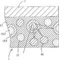
图4为本发明的载体内混有单层反射粒子、双层反射粒子、单层吸收粒子及双层吸收粒子实施例示意图。 Fig. 4 is a schematic diagram of an embodiment of a carrier of the present invention mixed with single-layer reflective particles, double-layer reflective particles, single-layer absorbing particles and double-layer absorbing particles. the
图5为本发明的制程步骤流程图 Fig. 5 is the process flow chart of the present invention
图6为本发明应用手机天线的实施例示意图。 Fig. 6 is a schematic diagram of an embodiment of the application of the mobile phone antenna in the present invention. the
图7为本发明应用于手机壳体的实施例示意图。 Fig. 7 is a schematic diagram of an embodiment of the present invention applied to a mobile phone casing. the
图中: In the picture:
1 复合层 1 composite layer
12 载体 12 carrier
14 粒子 14 particles
16 反射粒子 16 reflective particles
18 反射粒子 18 reflective particles
182 内层 182 inner layer
184 外层 184 outer layer
2 反射层 2 reflective layer
21 吸收粒子 21 absorb particles
22 吸收粒子 22 absorbing particles
222 内层 222 inner layer
224 外层 224 outer layer
24 胶层 24 Adhesive layer
26 绝缘层 26 insulation layer
3 天线 3 antenna
4 螺固组件 4 screw components
5 吸收薄膜 5 Absorbent film
6 欲屏蔽物 6 Desire to shield
7 壳体 7 shell
为了使审查员对本发明的结构特征及所达成的功效有更进一步的了解与认识,谨佐以较佳的实施例并配合附图对本发明做详细说明如后: In order to enable the examiner to have a further understanding and understanding of the structural features and the achieved effects of the present invention, the present invention will be described in detail with preferred embodiments and accompanying drawings as follows:
具体实施方式Detailed ways
本发明为一种电磁波吸收薄膜结构及其制造方法,其系藉由波相消干涉原理来达到将电磁波相消,以达到将电磁波吸收的目的。 The present invention is an electromagnetic wave absorbing film structure and its manufacturing method, which uses the principle of wave destructive interference to achieve the elimination of electromagnetic waves to achieve the purpose of absorbing electromagnetic waves. the
首先,先针对相消干涉(des劬ctiVe interference)的原理先进行说明,所谓相消干涉系当两列同源反向的波相遇,一列的波峰会叠加在另一列波的波谷上,使两个波互相抵消,以下本发明将以此一原理为基础,进行本发明的说明。 First, let’s explain the principle of destructive interference. The so-called destructive interference means that when two waves of the same source and opposite directions meet, the crest of one wave is superimposed on the trough of the other wave, so that the two The two waves cancel each other out, and the present invention will be described below based on this principle. the
请参阅图1,其系本发明的一实施例示意图,其中为便于了解本发明的电磁波吸收薄膜结构与欲屏蔽物问的位置关系,系于图中绘示出欲屏蔽物6。本发明主要包含有一以高分子聚合物为载体12而混入适当粒子14的复合层1与一位于复合层1上的反射层2。其中对于复合层1的厚度为满足波的相消干涉原理,乃采用所欲吸收的电磁波波长的 
下面针对上述本发明所混入粒子进行举例说明,首先该粒子14可以为反射粒子16,而反射粒子16更可为具有双层结构反射粒子18,其内层182为吸波材质,如碳化硅、麦饭石、远红外陶瓷、电气石等,而外层184为反射材质,如金属。请参阅图2,当电磁波射入的波行进方向遇到反射粒子18时,较低能量的波将被反射粒子18的外层184反射,但反射的波,将遭遇到另一反射粒子18,如此不断重复,而产生如消波堤的效果,使电磁波抵销;而穿射入反射粒子18内的电磁波将部分被内层182吸收,而、剩余穿透出的电磁波其能量将大幅度衰减,并在穿透内层182后面临外层184的折射,如此在反射粒子18内部不断折射、相消、吸收,而将电磁波抵销。 The following is an example for the above-mentioned particles mixed in the present invention. First, the particles 14 can be
本发明的反射粒子16也可采用部分反射粒子为具有双层结构的反射粒子18,部分粒子为单层结构的反射粒子16混合仅利用吸波材所构成的较小吸收粒子21混入高分子载体12内,以使高分子内的粒子分布更为紧密,而形成如同蜂窝状的复合层1,如此能更增加波于复合层1内折射、相消、吸收,如图3所示,此种方法,可避免高混合比例情况下,反射粒子16可能产生导通的问题。 The
请参阅第4图,更者,本发明的吸收粒子21也可以为具有双层结构的吸收粒子22,也就是内层222为反射材质,如金属,而外层224为吸波材质,如碳化硅、麦饭石、远红外陶瓷、电气石等。当电磁波遇到此一双层结构的吸收粒子22时,电磁波将先遭遇吸收,而通过外层的电磁波将遭遇到内层反射回外层吸收层,而大幅度降低电磁波的能量,甚至达到将电磁波完全吸收。 Please refer to Figure 4, moreover, the absorbing
当然,上述所提到的各种粒子,可以适当单独使用或者混合,以达到较佳吸收、抵销电磁波。 Of course, the various particles mentioned above can be used alone or mixed appropriately to achieve better absorption and cancellation of electromagnetic waves. the
下面继续对本发明的反射层2进行说明,本发明的反射层2系位于复合层1上,该反射层2系用以将能够穿越复合层1的电磁波反射回复合层1,因此,该反射层2的材料选用系依据复合层1的载体12来进行选择,使反射层2的折射率n1大于载体12的折射率n2,以使电磁波由密介质射向疏介质,以在符合布鲁斯特角(Brewsten angle)条件下,大幅度增加电磁波反射回复合层1的机会。一般而言,系采用一合金层来形成折射层2,也可由铝层、镍层、铁层、铜层以及钴层所组成的堆栈层;而当选定为合金层时其合金类别可选自铝、镍、铁、钴、铜所组成,另外也可添加微量的锰。 Continue to describe the
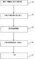
以下将对本发明的制造方法进行说明,请参阅图5,首先,如步骤S1所述提供一熔融态的高分子聚合物以作为载体12;接着,如步骤S2所述,于载体12中混入前述的粒子,其中混入的粒子选择,可依据前述所提到的反射粒子、吸收粒子、双层反射粒子、双层吸收粒子进行单独或混合选择;再如步骤S3所示,进行一成型制程,以使载体12成为复合层1,其中该成型制程时可藉由挤制过程将复合层1的膜厚形成所需厚度;最后,如步骤S4所示,于复合层1表面形成一反射层2,该反射层2的形成方法可选自于真空溅镀(vacuum sputter)、电镀等。更者,为便于本发明的吸收电磁波薄膜的应用,更可于复合层1的另一侧面进行一上胶步骤,以形 成一可供黏贴的胶层24,如步骤S5所示,或者是于反射层2的另一侧面上胶(其上胶位置的不同乃视欲黏贴位置不同而有差异),以便于使用者将本发明黏贴于所欲进行电磁波阻挡的位置,其中于反射层2的另一侧面上胶时,需先于反射层2的该侧面上形成一绝缘层26,以避免电流导通,其成品如图1所示。 The manufacturing method of the present invention will be described below. Please refer to FIG. 5. First, as described in step S1, a molten high molecular polymer is provided as the
下面将对本发明的应用在如手机等电磁波通讯器材上的实施例进行说明,首先请参阅图6所示,就应用在天线上来进行说明,手机藉由电磁波发射器与天线将电磁波讯号发射给基地台,因此天线往往是电磁波发出的位置,对于人体的影响也往往更为显著。本发明系针对此一问题,于天线外黏贴本发明的吸收电磁波薄膜,此一黏贴方式,如图6所示,系将天线3与螺固组件4外围皆形成或者黏贴上本发明的吸收薄膜5,但需保留一宽度”a”无黏贴或者形成本发明的吸收薄膜以供电磁波穿射出,该a宽度为手机发射的电磁波的波长的整数倍,且此一宽度a系朝向远离人体接触面的方向。更者,也可如图7所示,将本发明的吸收薄膜5黏贴在手机的壳体7内侧的适当位置,以达到更完善的电磁波防护。 The following will describe the embodiment of the present invention applied to electromagnetic wave communication equipment such as mobile phones. First, please refer to FIG. Therefore, the antenna is often the place where electromagnetic waves are emitted, and the impact on the human body is often more significant. The present invention is aimed at this problem. The electromagnetic wave absorbing film of the present invention is pasted on the outside of the antenna. This pasting method, as shown in FIG.
当然,上述所举例的方式是利用贴合方式来达成,另外也可藉由将如手机壳体的零组件作为基底,而将本发明的吸收电磁波吸收薄膜成型涂布于基底上,来达到吸收电磁波的功效。因此,当以零组件为基底时,本发明的电磁波吸收薄膜的制程将适度修正为先于零组件内表面上形成一反射层,随后将混合有粒子的复合层涂布于反射层上。然此一步骤上顺序的修改,凡是熟悉该项技术的人员,都能由本发明前述的步骤修改而得知,因此于此系不再赘述。 Certainly, the above-mentioned way of exemplifying is achieved by laminating. In addition, the electromagnetic wave absorbing film of the present invention can be formed and coated on the base by using components such as mobile phone casings as the base to achieve absorption. The effect of electromagnetic waves. Therefore, when the component is used as the substrate, the manufacturing process of the electromagnetic wave absorbing film of the present invention will be properly modified to form a reflective layer on the inner surface of the component, and then coat the composite layer mixed with particles on the reflective layer. However, those who are familiar with the technology can know the modification of the order of the steps by modifying the aforementioned steps of the present invention, so it is not repeated here. the
综上所述,本发明为一种电磁波吸收薄膜结构及其制造方法,其主要系利用波的相位相消特性与折射、吸收,使电磁波间产生抵销,因此,将不会产生一般使用金属屏蔽材时,需接地以将受驱使电子导流的必要,更者,本发明以相位相消的原理为基础下,仅需一复合层即可达到将电磁波消除的目的,将使得防电磁波材进入一崭新轻薄化的技术领域。 In summary, the present invention is an electromagnetic wave absorbing thin film structure and its manufacturing method, which mainly utilizes the phase cancellation characteristics, refraction, and absorption of waves to cause offset between electromagnetic waves. When shielding materials, it is necessary to be grounded to guide the driven electrons. What's more, the present invention is based on the principle of phase cancellation, and only one composite layer is needed to achieve the purpose of eliminating electromagnetic waves, which will make the anti-electromagnetic wave material Enter a new thin and light technical field. the
惟以上所述者,仅为本发明一较佳实施例而已,并非用来限定本发明实施的范围,故凡依本发明申请专利范围所述的形状、构造、特征及精神所为的均等变化与修饰,均应包括于本发明的申请的权利要求的保护范围内。 But what is described above is only a preferred embodiment of the present invention, and is not used to limit the scope of the present invention, so all equal changes are made according to the shape, structure, characteristics and spirit described in the patent scope of the present invention All modifications and modifications should be included within the protection scope of the claims of the application of the present invention. the
Claims (5)

Priority Applications (1)
| Application Number | Priority Date | Filing Date | Title |
|---|---|---|---|
| CN2005100855250ACN1905789B (en) | 2005-07-26 | 2005-07-26 | Electromagnetic wave absorbing thin film structure and manufacturing method thereof |
Applications Claiming Priority (1)
| Application Number | Priority Date | Filing Date | Title |
|---|---|---|---|
| CN2005100855250ACN1905789B (en) | 2005-07-26 | 2005-07-26 | Electromagnetic wave absorbing thin film structure and manufacturing method thereof |
Publications (2)
| Publication Number | Publication Date |
|---|---|
| CN1905789A CN1905789A (en) | 2007-01-31 |
| CN1905789Btrue CN1905789B (en) | 2011-02-23 |
Family
ID=37674870
Family Applications (1)
| Application Number | Title | Priority Date | Filing Date |
|---|---|---|---|
| CN2005100855250AExpired - Fee RelatedCN1905789B (en) | 2005-07-26 | 2005-07-26 | Electromagnetic wave absorbing thin film structure and manufacturing method thereof |
Country Status (1)
| Country | Link |
|---|---|
| CN (1) | CN1905789B (en) |
Families Citing this family (12)
| Publication number | Priority date | Publication date | Assignee | Title |
|---|---|---|---|---|
| AU2008335462B2 (en)* | 2007-12-06 | 2014-02-20 | Cardiac Pacemakers, Inc. | Implantable lead having a variable coil conductor pitch |
| US9084883B2 (en) | 2009-03-12 | 2015-07-21 | Cardiac Pacemakers, Inc. | Thin profile conductor assembly for medical device leads |
| US9254380B2 (en) | 2009-10-19 | 2016-02-09 | Cardiac Pacemakers, Inc. | MRI compatible tachycardia lead |
| US9750944B2 (en) | 2009-12-30 | 2017-09-05 | Cardiac Pacemakers, Inc. | MRI-conditionally safe medical device lead |
| US8391994B2 (en) | 2009-12-31 | 2013-03-05 | Cardiac Pacemakers, Inc. | MRI conditionally safe lead with low-profile multi-layer conductor for longitudinal expansion |
| WO2011081713A1 (en) | 2009-12-31 | 2011-07-07 | Cardiac Pacemakers, Inc. | Mri conditionally safe lead with multi-layer conductor |
| CN103035304A (en)* | 2011-09-28 | 2013-04-10 | 洪荣泰 | Electromagnetic Wave Isolation Device |
| US8954168B2 (en) | 2012-06-01 | 2015-02-10 | Cardiac Pacemakers, Inc. | Implantable device lead including a distal electrode assembly with a coiled component |
| JP6069499B2 (en) | 2012-08-31 | 2017-02-01 | カーディアック ペースメイカーズ, インコーポレイテッド | Lead wire with low peak MRI heating |
| US8983623B2 (en) | 2012-10-18 | 2015-03-17 | Cardiac Pacemakers, Inc. | Inductive element for providing MRI compatibility in an implantable medical device lead |
| WO2015130753A1 (en) | 2014-02-26 | 2015-09-03 | Cardiac Pacemakers, Inc | Construction of an mri-safe tachycardia lead |
| CN106381573B (en)* | 2016-08-31 | 2018-12-28 | 诸暨市新丝维纤维有限公司 | A kind of anti-radiation fiber of active absorption formula |
Citations (4)
| Publication number | Priority date | Publication date | Assignee | Title |
|---|---|---|---|---|
| FR1481906A (en)* | 1961-02-02 | 1967-05-26 | Eltro Gmbh | Device for absorbing electromagnetic waves by interference |
| US6805817B2 (en)* | 2000-12-14 | 2004-10-19 | Hewlett-Packard Development Company, L.P. | Molecular devices activated by an electric field for electronic ink and other visual display |
| US20040234750A1 (en)* | 2003-05-19 | 2004-11-25 | Li-Hsien Yen | [multilayer structure for absorbing electromagnatic wave and manufacturing method thereof] |
| CN2701181Y (en)* | 2002-10-24 | 2005-05-18 | 朱炜 | Radiation shield assembly for mobile phone |
- 2005
- 2005-07-26CNCN2005100855250Apatent/CN1905789B/ennot_activeExpired - Fee Related
Patent Citations (4)
| Publication number | Priority date | Publication date | Assignee | Title |
|---|---|---|---|---|
| FR1481906A (en)* | 1961-02-02 | 1967-05-26 | Eltro Gmbh | Device for absorbing electromagnetic waves by interference |
| US6805817B2 (en)* | 2000-12-14 | 2004-10-19 | Hewlett-Packard Development Company, L.P. | Molecular devices activated by an electric field for electronic ink and other visual display |
| CN2701181Y (en)* | 2002-10-24 | 2005-05-18 | 朱炜 | Radiation shield assembly for mobile phone |
| US20040234750A1 (en)* | 2003-05-19 | 2004-11-25 | Li-Hsien Yen | [multilayer structure for absorbing electromagnatic wave and manufacturing method thereof] |
Non-Patent Citations (1)
| Title |
|---|
| 同上. |
Also Published As
| Publication number | Publication date |
|---|---|
| CN1905789A (en) | 2007-01-31 |
Similar Documents
| Publication | Publication Date | Title |
|---|---|---|
| CN1905789B (en) | Electromagnetic wave absorbing thin film structure and manufacturing method thereof | |
| JP7267912B2 (en) | electromagnetic wave absorption sheet | |
| KR101759580B1 (en) | Multi-layered electromagnetic wave absorber and method for producing a multi-layered electromagnetic wave absorber | |
| CN106413359B (en) | Bidirectional absorbing strong electromagnetic shielding light window of multilayer graphene grid/metal grid stack structure | |
| CN105655721A (en) | Double-waveband composite broadband wave absorbing material based on frequency selective surface | |
| CN106413358A (en) | Electromagnetic shielding optical window based on graphene/transparent conductive film composite structure | |
| US7242507B2 (en) | Electromagnetic wave absorptive film and its fabrication | |
| CN111970915A (en) | Electromagnetic radiation prevention ultrathin film, electromagnetic radiation prevention ultrathin film device, preparation method and application | |
| CN102781206B (en) | A kind of suction ripple Meta Materials | |
| CN106413364A (en) | Bidirectional wave absorption transparent electromagnetic shielding device based on graphene/transparent conductive films | |
| CN108617161A (en) | A kind of ultra-thin anti-EMI filter film and preparation method thereof | |
| CN106714533B (en) | Transparent bidirectional wave-absorbing electromagnetic shielding device with graphene and double-layer metal mesh grid | |
| CN106413357B (en) | Electromagnetic Shielding Light Window Based on Laminated Structure of Graphene Grid and Transparent Conductive Film | |
| CN111726976B (en) | Electromagnetic wave shielding piece, transmission line assembly and electronic packaging structure applying same | |
| CN106413362A (en) | Bidirectional wave absorption transparent electromagnetic shielding device based on graphene meshes and transparent conductive films | |
| TWI685080B (en) | Electromagnetic wave shilding element, and transmission line assembly and electronic package structure using the same | |
| CN106413365B (en) | Strong Electromagnetic Shielding Light Window Based on Graphene and Double Metal Grid Laminated Structure | |
| KR100897309B1 (en) | Electromagnetic wave absorbing film and manufacturing method thereof | |
| CN211607245U (en) | Low-frequency shielding heat-conducting composite structure | |
| TWI249469B (en) | Electromagnetic wave absorbing film structure and the manufacture method thereof | |
| JP2007036081A (en) | Microwave-absorbing film structure and its manufacturing method | |
| JP5234673B2 (en) | Interference type radio wave shield or absorber | |
| CN106413361B (en) | Electromagnetic shielding optical window with double graphene absorption layers and double metal mesh grid structures | |
| MXPA05009460A (en) | Electromagnetic wave absorptive film and its fabrication. | |
| NZ542021A (en) | Electromagnetic wave absorptive film and it's fabrication |
Legal Events
| Date | Code | Title | Description |
|---|---|---|---|
| C06 | Publication | ||
| PB01 | Publication | ||
| C10 | Entry into substantive examination | ||
| SE01 | Entry into force of request for substantive examination | ||
| C14 | Grant of patent or utility model | ||
| GR01 | Patent grant | ||
| CF01 | Termination of patent right due to non-payment of annual fee | Granted publication date:20110223 Termination date:20170726 | |
| CF01 | Termination of patent right due to non-payment of annual fee |