CN1901179A - Tape wiring substrate and chip-on-film package using the same - Google Patents
Tape wiring substrate and chip-on-film package using the sameDownload PDFInfo
- Publication number
- CN1901179A CN1901179ACNA2006100678640ACN200610067864ACN1901179ACN 1901179 ACN1901179 ACN 1901179ACN A2006100678640 ACNA2006100678640 ACN A2006100678640ACN 200610067864 ACN200610067864 ACN 200610067864ACN 1901179 ACN1901179 ACN 1901179A
- Authority
- CN
- China
- Prior art keywords
- ground plane
- pseudo
- metal layer
- ground
- semiconductor chip
- Prior art date
- Legal status (The legal status is an assumption and is not a legal conclusion. Google has not performed a legal analysis and makes no representation as to the accuracy of the status listed.)
- Granted
Links
Images


Classifications
- H—ELECTRICITY
- H01—ELECTRIC ELEMENTS
- H01L—SEMICONDUCTOR DEVICES NOT COVERED BY CLASS H10
- H01L23/00—Details of semiconductor or other solid state devices
- H01L23/12—Mountings, e.g. non-detachable insulating substrates
- H—ELECTRICITY
- H01—ELECTRIC ELEMENTS
- H01L—SEMICONDUCTOR DEVICES NOT COVERED BY CLASS H10
- H01L23/00—Details of semiconductor or other solid state devices
- H01L23/552—Protection against radiation, e.g. light or electromagnetic waves
- H—ELECTRICITY
- H01—ELECTRIC ELEMENTS
- H01L—SEMICONDUCTOR DEVICES NOT COVERED BY CLASS H10
- H01L23/00—Details of semiconductor or other solid state devices
- H01L23/34—Arrangements for cooling, heating, ventilating or temperature compensation ; Temperature sensing arrangements
- H01L23/36—Selection of materials, or shaping, to facilitate cooling or heating, e.g. heatsinks
- H01L23/367—Cooling facilitated by shape of device
- H01L23/3677—Wire-like or pin-like cooling fins or heat sinks
- H—ELECTRICITY
- H01—ELECTRIC ELEMENTS
- H01L—SEMICONDUCTOR DEVICES NOT COVERED BY CLASS H10
- H01L23/00—Details of semiconductor or other solid state devices
- H01L23/48—Arrangements for conducting electric current to or from the solid state body in operation, e.g. leads, terminal arrangements ; Selection of materials therefor
- H01L23/488—Arrangements for conducting electric current to or from the solid state body in operation, e.g. leads, terminal arrangements ; Selection of materials therefor consisting of soldered or bonded constructions
- H01L23/498—Leads, i.e. metallisations or lead-frames on insulating substrates, e.g. chip carriers
- H01L23/49838—Geometry or layout
- H—ELECTRICITY
- H01—ELECTRIC ELEMENTS
- H01L—SEMICONDUCTOR DEVICES NOT COVERED BY CLASS H10
- H01L23/00—Details of semiconductor or other solid state devices
- H01L23/48—Arrangements for conducting electric current to or from the solid state body in operation, e.g. leads, terminal arrangements ; Selection of materials therefor
- H01L23/488—Arrangements for conducting electric current to or from the solid state body in operation, e.g. leads, terminal arrangements ; Selection of materials therefor consisting of soldered or bonded constructions
- H01L23/498—Leads, i.e. metallisations or lead-frames on insulating substrates, e.g. chip carriers
- H01L23/4985—Flexible insulating substrates
- H—ELECTRICITY
- H01—ELECTRIC ELEMENTS
- H01L—SEMICONDUCTOR DEVICES NOT COVERED BY CLASS H10
- H01L23/00—Details of semiconductor or other solid state devices
- H01L23/48—Arrangements for conducting electric current to or from the solid state body in operation, e.g. leads, terminal arrangements ; Selection of materials therefor
- H01L23/50—Arrangements for conducting electric current to or from the solid state body in operation, e.g. leads, terminal arrangements ; Selection of materials therefor for integrated circuit devices, e.g. power bus, number of leads
- H—ELECTRICITY
- H01—ELECTRIC ELEMENTS
- H01L—SEMICONDUCTOR DEVICES NOT COVERED BY CLASS H10
- H01L24/00—Arrangements for connecting or disconnecting semiconductor or solid-state bodies; Methods or apparatus related thereto
- H01L24/01—Means for bonding being attached to, or being formed on, the surface to be connected, e.g. chip-to-package, die-attach, "first-level" interconnects; Manufacturing methods related thereto
- H01L24/10—Bump connectors ; Manufacturing methods related thereto
- H01L24/15—Structure, shape, material or disposition of the bump connectors after the connecting process
- H01L24/17—Structure, shape, material or disposition of the bump connectors after the connecting process of a plurality of bump connectors
- H—ELECTRICITY
- H05—ELECTRIC TECHNIQUES NOT OTHERWISE PROVIDED FOR
- H05K—PRINTED CIRCUITS; CASINGS OR CONSTRUCTIONAL DETAILS OF ELECTRIC APPARATUS; MANUFACTURE OF ASSEMBLAGES OF ELECTRICAL COMPONENTS
- H05K1/00—Printed circuits
- H05K1/02—Details
- H05K1/0213—Electrical arrangements not otherwise provided for
- H05K1/0216—Reduction of cross-talk, noise or electromagnetic interference
- H—ELECTRICITY
- H01—ELECTRIC ELEMENTS
- H01L—SEMICONDUCTOR DEVICES NOT COVERED BY CLASS H10
- H01L2224/00—Indexing scheme for arrangements for connecting or disconnecting semiconductor or solid-state bodies and methods related thereto as covered by H01L24/00
- H01L2224/01—Means for bonding being attached to, or being formed on, the surface to be connected, e.g. chip-to-package, die-attach, "first-level" interconnects; Manufacturing methods related thereto
- H01L2224/02—Bonding areas; Manufacturing methods related thereto
- H01L2224/04—Structure, shape, material or disposition of the bonding areas prior to the connecting process
- H01L2224/05—Structure, shape, material or disposition of the bonding areas prior to the connecting process of an individual bonding area
- H01L2224/0554—External layer
- H01L2224/0556—Disposition
- H01L2224/05571—Disposition the external layer being disposed in a recess of the surface
- H—ELECTRICITY
- H01—ELECTRIC ELEMENTS
- H01L—SEMICONDUCTOR DEVICES NOT COVERED BY CLASS H10
- H01L2224/00—Indexing scheme for arrangements for connecting or disconnecting semiconductor or solid-state bodies and methods related thereto as covered by H01L24/00
- H01L2224/01—Means for bonding being attached to, or being formed on, the surface to be connected, e.g. chip-to-package, die-attach, "first-level" interconnects; Manufacturing methods related thereto
- H01L2224/02—Bonding areas; Manufacturing methods related thereto
- H01L2224/04—Structure, shape, material or disposition of the bonding areas prior to the connecting process
- H01L2224/05—Structure, shape, material or disposition of the bonding areas prior to the connecting process of an individual bonding area
- H01L2224/0554—External layer
- H01L2224/05573—Single external layer
- H—ELECTRICITY
- H01—ELECTRIC ELEMENTS
- H01L—SEMICONDUCTOR DEVICES NOT COVERED BY CLASS H10
- H01L2224/00—Indexing scheme for arrangements for connecting or disconnecting semiconductor or solid-state bodies and methods related thereto as covered by H01L24/00
- H01L2224/01—Means for bonding being attached to, or being formed on, the surface to be connected, e.g. chip-to-package, die-attach, "first-level" interconnects; Manufacturing methods related thereto
- H01L2224/02—Bonding areas; Manufacturing methods related thereto
- H01L2224/04—Structure, shape, material or disposition of the bonding areas prior to the connecting process
- H01L2224/06—Structure, shape, material or disposition of the bonding areas prior to the connecting process of a plurality of bonding areas
- H01L2224/061—Disposition
- H01L2224/0612—Layout
- H01L2224/0613—Square or rectangular array
- H01L2224/06134—Square or rectangular array covering only portions of the surface to be connected
- H01L2224/06135—Covering only the peripheral area of the surface to be connected, i.e. peripheral arrangements
- H—ELECTRICITY
- H01—ELECTRIC ELEMENTS
- H01L—SEMICONDUCTOR DEVICES NOT COVERED BY CLASS H10
- H01L2224/00—Indexing scheme for arrangements for connecting or disconnecting semiconductor or solid-state bodies and methods related thereto as covered by H01L24/00
- H01L2224/01—Means for bonding being attached to, or being formed on, the surface to be connected, e.g. chip-to-package, die-attach, "first-level" interconnects; Manufacturing methods related thereto
- H01L2224/10—Bump connectors; Manufacturing methods related thereto
- H01L2224/12—Structure, shape, material or disposition of the bump connectors prior to the connecting process
- H01L2224/13—Structure, shape, material or disposition of the bump connectors prior to the connecting process of an individual bump connector
- H01L2224/13001—Core members of the bump connector
- H01L2224/13099—Material
- H—ELECTRICITY
- H01—ELECTRIC ELEMENTS
- H01L—SEMICONDUCTOR DEVICES NOT COVERED BY CLASS H10
- H01L2224/00—Indexing scheme for arrangements for connecting or disconnecting semiconductor or solid-state bodies and methods related thereto as covered by H01L24/00
- H01L2224/01—Means for bonding being attached to, or being formed on, the surface to be connected, e.g. chip-to-package, die-attach, "first-level" interconnects; Manufacturing methods related thereto
- H01L2224/10—Bump connectors; Manufacturing methods related thereto
- H01L2224/15—Structure, shape, material or disposition of the bump connectors after the connecting process
- H01L2224/16—Structure, shape, material or disposition of the bump connectors after the connecting process of an individual bump connector
- H01L2224/161—Disposition
- H01L2224/16151—Disposition the bump connector connecting between a semiconductor or solid-state body and an item not being a semiconductor or solid-state body, e.g. chip-to-substrate, chip-to-passive
- H01L2224/16221—Disposition the bump connector connecting between a semiconductor or solid-state body and an item not being a semiconductor or solid-state body, e.g. chip-to-substrate, chip-to-passive the body and the item being stacked
- H01L2224/16225—Disposition the bump connector connecting between a semiconductor or solid-state body and an item not being a semiconductor or solid-state body, e.g. chip-to-substrate, chip-to-passive the body and the item being stacked the item being non-metallic, e.g. insulating substrate with or without metallisation
- H—ELECTRICITY
- H01—ELECTRIC ELEMENTS
- H01L—SEMICONDUCTOR DEVICES NOT COVERED BY CLASS H10
- H01L2224/00—Indexing scheme for arrangements for connecting or disconnecting semiconductor or solid-state bodies and methods related thereto as covered by H01L24/00
- H01L2224/01—Means for bonding being attached to, or being formed on, the surface to be connected, e.g. chip-to-package, die-attach, "first-level" interconnects; Manufacturing methods related thereto
- H01L2224/26—Layer connectors, e.g. plate connectors, solder or adhesive layers; Manufacturing methods related thereto
- H01L2224/31—Structure, shape, material or disposition of the layer connectors after the connecting process
- H01L2224/32—Structure, shape, material or disposition of the layer connectors after the connecting process of an individual layer connector
- H01L2224/321—Disposition
- H01L2224/32151—Disposition the layer connector connecting between a semiconductor or solid-state body and an item not being a semiconductor or solid-state body, e.g. chip-to-substrate, chip-to-passive
- H01L2224/32221—Disposition the layer connector connecting between a semiconductor or solid-state body and an item not being a semiconductor or solid-state body, e.g. chip-to-substrate, chip-to-passive the body and the item being stacked
- H01L2224/32225—Disposition the layer connector connecting between a semiconductor or solid-state body and an item not being a semiconductor or solid-state body, e.g. chip-to-substrate, chip-to-passive the body and the item being stacked the item being non-metallic, e.g. insulating substrate with or without metallisation
- H—ELECTRICITY
- H01—ELECTRIC ELEMENTS
- H01L—SEMICONDUCTOR DEVICES NOT COVERED BY CLASS H10
- H01L2224/00—Indexing scheme for arrangements for connecting or disconnecting semiconductor or solid-state bodies and methods related thereto as covered by H01L24/00
- H01L2224/73—Means for bonding being of different types provided for in two or more of groups H01L2224/10, H01L2224/18, H01L2224/26, H01L2224/34, H01L2224/42, H01L2224/50, H01L2224/63, H01L2224/71
- H01L2224/732—Location after the connecting process
- H01L2224/73201—Location after the connecting process on the same surface
- H01L2224/73203—Bump and layer connectors
- H01L2224/73204—Bump and layer connectors the bump connector being embedded into the layer connector
- H—ELECTRICITY
- H01—ELECTRIC ELEMENTS
- H01L—SEMICONDUCTOR DEVICES NOT COVERED BY CLASS H10
- H01L23/00—Details of semiconductor or other solid state devices
- H01L23/34—Arrangements for cooling, heating, ventilating or temperature compensation ; Temperature sensing arrangements
- H01L23/36—Selection of materials, or shaping, to facilitate cooling or heating, e.g. heatsinks
- H—ELECTRICITY
- H01—ELECTRIC ELEMENTS
- H01L—SEMICONDUCTOR DEVICES NOT COVERED BY CLASS H10
- H01L2924/00—Indexing scheme for arrangements or methods for connecting or disconnecting semiconductor or solid-state bodies as covered by H01L24/00
- H01L2924/0001—Technical content checked by a classifier
- H01L2924/00014—Technical content checked by a classifier the subject-matter covered by the group, the symbol of which is combined with the symbol of this group, being disclosed without further technical details
- H—ELECTRICITY
- H01—ELECTRIC ELEMENTS
- H01L—SEMICONDUCTOR DEVICES NOT COVERED BY CLASS H10
- H01L2924/00—Indexing scheme for arrangements or methods for connecting or disconnecting semiconductor or solid-state bodies as covered by H01L24/00
- H01L2924/01—Chemical elements
- H01L2924/01006—Carbon [C]
- H—ELECTRICITY
- H01—ELECTRIC ELEMENTS
- H01L—SEMICONDUCTOR DEVICES NOT COVERED BY CLASS H10
- H01L2924/00—Indexing scheme for arrangements or methods for connecting or disconnecting semiconductor or solid-state bodies as covered by H01L24/00
- H01L2924/01—Chemical elements
- H01L2924/01015—Phosphorus [P]
- H—ELECTRICITY
- H01—ELECTRIC ELEMENTS
- H01L—SEMICONDUCTOR DEVICES NOT COVERED BY CLASS H10
- H01L2924/00—Indexing scheme for arrangements or methods for connecting or disconnecting semiconductor or solid-state bodies as covered by H01L24/00
- H01L2924/01—Chemical elements
- H01L2924/01029—Copper [Cu]
- H—ELECTRICITY
- H01—ELECTRIC ELEMENTS
- H01L—SEMICONDUCTOR DEVICES NOT COVERED BY CLASS H10
- H01L2924/00—Indexing scheme for arrangements or methods for connecting or disconnecting semiconductor or solid-state bodies as covered by H01L24/00
- H01L2924/01—Chemical elements
- H01L2924/01033—Arsenic [As]
- H—ELECTRICITY
- H01—ELECTRIC ELEMENTS
- H01L—SEMICONDUCTOR DEVICES NOT COVERED BY CLASS H10
- H01L2924/00—Indexing scheme for arrangements or methods for connecting or disconnecting semiconductor or solid-state bodies as covered by H01L24/00
- H01L2924/01—Chemical elements
- H01L2924/01079—Gold [Au]
- H—ELECTRICITY
- H01—ELECTRIC ELEMENTS
- H01L—SEMICONDUCTOR DEVICES NOT COVERED BY CLASS H10
- H01L2924/00—Indexing scheme for arrangements or methods for connecting or disconnecting semiconductor or solid-state bodies as covered by H01L24/00
- H01L2924/01—Chemical elements
- H01L2924/01082—Lead [Pb]
- H—ELECTRICITY
- H01—ELECTRIC ELEMENTS
- H01L—SEMICONDUCTOR DEVICES NOT COVERED BY CLASS H10
- H01L2924/00—Indexing scheme for arrangements or methods for connecting or disconnecting semiconductor or solid-state bodies as covered by H01L24/00
- H01L2924/013—Alloys
- H01L2924/014—Solder alloys
- H—ELECTRICITY
- H01—ELECTRIC ELEMENTS
- H01L—SEMICONDUCTOR DEVICES NOT COVERED BY CLASS H10
- H01L2924/00—Indexing scheme for arrangements or methods for connecting or disconnecting semiconductor or solid-state bodies as covered by H01L24/00
- H01L2924/15—Details of package parts other than the semiconductor or other solid state devices to be connected
- H01L2924/181—Encapsulation
- H—ELECTRICITY
- H05—ELECTRIC TECHNIQUES NOT OTHERWISE PROVIDED FOR
- H05K—PRINTED CIRCUITS; CASINGS OR CONSTRUCTIONAL DETAILS OF ELECTRIC APPARATUS; MANUFACTURE OF ASSEMBLAGES OF ELECTRICAL COMPONENTS
- H05K1/00—Printed circuits
- H05K1/02—Details
- H05K1/11—Printed elements for providing electric connections to or between printed circuits
- H05K1/111—Pads for surface mounting, e.g. lay-out
- H05K1/112—Pads for surface mounting, e.g. lay-out directly combined with via connections
- H05K1/113—Via provided in pad; Pad over filled via
- H—ELECTRICITY
- H05—ELECTRIC TECHNIQUES NOT OTHERWISE PROVIDED FOR
- H05K—PRINTED CIRCUITS; CASINGS OR CONSTRUCTIONAL DETAILS OF ELECTRIC APPARATUS; MANUFACTURE OF ASSEMBLAGES OF ELECTRICAL COMPONENTS
- H05K1/00—Printed circuits
- H05K1/18—Printed circuits structurally associated with non-printed electric components
- H05K1/189—Printed circuits structurally associated with non-printed electric components characterised by the use of a flexible or folded printed circuit
- H—ELECTRICITY
- H05—ELECTRIC TECHNIQUES NOT OTHERWISE PROVIDED FOR
- H05K—PRINTED CIRCUITS; CASINGS OR CONSTRUCTIONAL DETAILS OF ELECTRIC APPARATUS; MANUFACTURE OF ASSEMBLAGES OF ELECTRICAL COMPONENTS
- H05K2201/00—Indexing scheme relating to printed circuits covered by H05K1/00
- H05K2201/07—Electric details
- H05K2201/0707—Shielding
- H05K2201/0715—Shielding provided by an outer layer of PCB
- H—ELECTRICITY
- H05—ELECTRIC TECHNIQUES NOT OTHERWISE PROVIDED FOR
- H05K—PRINTED CIRCUITS; CASINGS OR CONSTRUCTIONAL DETAILS OF ELECTRIC APPARATUS; MANUFACTURE OF ASSEMBLAGES OF ELECTRICAL COMPONENTS
- H05K2201/00—Indexing scheme relating to printed circuits covered by H05K1/00
- H05K2201/09—Shape and layout
- H05K2201/09209—Shape and layout details of conductors
- H05K2201/0929—Conductive planes
- H05K2201/09318—Core having one signal plane and one power plane
Landscapes
- Physics & Mathematics (AREA)
- Engineering & Computer Science (AREA)
- Microelectronics & Electronic Packaging (AREA)
- Computer Hardware Design (AREA)
- Power Engineering (AREA)
- Condensed Matter Physics & Semiconductors (AREA)
- General Physics & Mathematics (AREA)
- Electromagnetism (AREA)
- Health & Medical Sciences (AREA)
- Geometry (AREA)
- Toxicology (AREA)
- Chemical & Material Sciences (AREA)
- Materials Engineering (AREA)
- Wire Bonding (AREA)
- Structure Of Printed Boards (AREA)
- Structures Or Materials For Encapsulating Or Coating Semiconductor Devices Or Solid State Devices (AREA)
Abstract
Translated fromChinese
Description
Translated fromChinese技术领域technical field
本发明的示范性实施例总体上涉及一种带布线基板(tape wiringsubstrate)以及利用该带布线基板的带封装,更具体而言,涉及一种具有双金属层的带布线基板以及实现该带布线基板的薄膜上芯片封装。Exemplary embodiments of the present invention generally relate to a tape wiring substrate and a tape package using the same, and more particularly, to a tape wiring substrate having a double metal layer and realizing the tape wiring substrate. Thin film chip-on-substrate packaging.
背景技术Background technique
平板显示器可以包括例如用于便携式电话的液晶显示器(“LCD”)、用于计算机的薄膜晶体管液晶显示器(“TFT LCD”)和家用的等离子体显示面板(“PDP”)。平板显示器可以包括本领域中公知的带封装部件。在某些应用中,带封装可以具有细距布线图案。Flat panel displays may include, for example, liquid crystal displays ("LCDs") for cellular phones, thin film transistor liquid crystal displays ("TFT LCDs") for computers, and plasma display panels ("PDPs") for home use. Flat panel displays may include packaged components known in the art. In some applications, a tape package may have a fine pitch wiring pattern.
带封装可以包括带布线基板。带封装的两种主要类型可以是带载封装(“TCP”)和薄膜上芯片(“COF”)封装。TCP的带布线基板可以具有芯片安装窗口,其中可以经由(例如)内引脚键合方法来安装半导体芯片。COF的带布线基板可以不包括芯片安装窗口。此时,半导体芯片可以被倒装芯片式键合到带布线基板。与TCP相比,COF封装可以允许更薄的带布线基板和/或更细节距的布线图案。The tape package may include a tape wiring substrate. Two main types of tape packages can be tape carrier packages ("TCP") and chip-on-film ("COF") packages. The substrate with wiring of TCP may have a chip mounting window in which a semiconductor chip may be mounted via, for example, an in-pin bonding method. The substrate with wiring of COF may not include a chip mounting window. At this time, the semiconductor chip can be flip-chip bonded to the wiring substrate. Compared to TCP, COF packages may allow thinner wiring substrates and/or finer pitch wiring patterns.
在COF封装中,I/O端子图案可以取代焊料凸点而起到外部连接端子的作用。I/O端子图案可以直接附着到印刷电路板或显示面板。In the COF package, I/O terminal patterns may function as external connection terminals instead of solder bumps. The I/O terminal pattern can be directly attached to a printed circuit board or a display panel.
图1是常规COF封装100的平面图。图2是沿图1的II-II线得到的横截面图。FIG. 1 is a plan view of a
参照图1和2,COF封装100可以包括带布线基板20。半导体芯片10可以被倒装芯片式键合到带布线基板20。模塑料(molding compound)40可以通过下填充工艺(underfill process)密封被倒装芯片式键合的部分。Referring to FIGS. 1 and 2 , the
半导体芯片10可以具有可支撑电极焊盘12的有源表面。可以沿该有源表面的边缘部分设置电极焊盘12。电极凸点16可以设置在电极焊盘12上。电极凸点16可以包括例如输入凸点17和输出凸点18。输入凸点17可以包括例如接地凸点17a和电源凸点17b。The
带布线基板20可以包括基薄膜21以及设置在基薄膜21的上表面22上的上金属层24。基薄膜21可以具有面对半导体芯片10的芯片安装区域。芯片安装区域可以位于基薄膜21的中心部分。基薄膜21可以包括定位孔(sprocket holes)29。定位孔29可以沿着基薄膜21以预定间距排列。上金属层24的一端可以连接到电极凸点16。上金属层24的另一端可以从芯片安装区域向外延伸。上金属层24可以包括输入端子图案25和输出端子图案26。输入端子图案25可以包括用于地的输入端子图案25a(“接地端子图案”)和用于电源的输入端子图案25b(“电源端子图案”)。输入端子图案25可以延伸到相对于半导体芯片10的基薄膜21的一侧,输出端子图案26可以延伸到相对于半导体芯片10的基薄膜21的另一侧。输入和输出端子图案25和26可以平行于定位孔29的设置而延伸。The substrate with
当半导体芯片10被倒装芯片式键合到带布线基板20时,接地凸点17a可以键合到接地端子图案25a,并且电源凸点17b可以键合到电源端子图案25b。When the
虽然常规COF封装通常被认为是可接受的,但其并非没有缺点。例如,为了有助于实现重量更轻、尺寸更小、速度更快、多功能和/或性能增强的半导体产品,可以使上金属层24具有细距布线图案,使半导体芯片10更加小型化,并且可以增大电极凸点16的数目。因此,接地端子图案25a和电源端子图案25b在节距上减小。例如,为了稳定的接地和/或电源,设置在基薄膜21的上表面22上的接地端子图案25a和电源端子图案25b可能具有不足的面积。While conventional COF packaging is generally considered acceptable, it is not without its drawbacks. For example, in order to help realize semiconductor products with lighter weight, smaller size, faster speed, multi-function and/or performance enhancement, the
常规COF封装100不能充分减小有可能在半导体芯片10的工作期间产生的电磁波和/或噪声,这会导致差的电磁干扰和/或噪声特性。此外,常规COF封装100有可能向半导体芯片10不稳定地供电。The
发明内容Contents of the invention
根据一示范性非限制实施例,带布线基板可以包括薄膜,所述薄膜含有包括芯片安装区域的上表面、下表面和穿通所述薄膜的通路。上金属层可以设置在所述薄膜的上表面上并连接到半导体芯片的电极凸点。所述上金属层可以包括输入端子图案和输出端子图案。所述上金属层可以仅延伸到所述芯片安装区域的外围区域上。下金属层可以设置在所述薄膜的下表面上。所述下金属层包括接地层。According to an exemplary non-limiting embodiment, the substrate with wiring may include a thin film having an upper surface including a chip mounting area, a lower surface, and a via passing through the thin film. An upper metal layer may be disposed on the upper surface of the thin film and connected to electrode bumps of the semiconductor chip. The upper metal layer may include input terminal patterns and output terminal patterns. The upper metal layer may extend only onto a peripheral area of the chip mounting area. A lower metal layer may be provided on the lower surface of the thin film. The lower metal layer includes a ground layer.
根据另一示范性非限制实施例,封装可以包括含有带电极凸点的有源表面的半导体芯片。可以设置带布线基板,其上安装了所述半导体芯片,使得所述电极凸点可以面对所述带布线基板。模塑料可以设置在所述半导体芯片和所述带布线基板之间。所述带布线基板可以包括薄膜,所述薄膜含有包括芯片安装区域的上表面、下表面和穿通所述薄膜的通路。上金属层可以设置在所述薄膜的上表面上并连接到所述电极凸点。所述上金属层可以包括输入端子图案和输出端子图案。所述上金属层可以仅延伸到所述芯片安装区域的外围区域上。下金属层可以设置在所述薄膜的下表面上。所述下金属层包括接地层。According to another exemplary non-limiting embodiment, a package may include a semiconductor chip having an active surface with electrode bumps. A substrate with wiring may be provided on which the semiconductor chip is mounted so that the electrode bumps may face the substrate with wiring. A molding compound may be provided between the semiconductor chip and the tape wiring substrate. The substrate with wiring may include a thin film having an upper surface including a chip mounting area, a lower surface, and a via passing through the thin film. An upper metal layer may be disposed on the upper surface of the thin film and connected to the electrode bumps. The upper metal layer may include input terminal patterns and output terminal patterns. The upper metal layer may extend only onto a peripheral area of the chip mounting area. A lower metal layer may be provided on the lower surface of the thin film. The lower metal layer includes a ground layer.
附图说明Description of drawings
通过结合附图参照以下提供的详细说明,能够更容易地理解本发明的示范性非限制实施例,其中相似的附图标记表示相似的结构部件。Exemplary, non-limiting embodiments of the present invention can be more readily understood by referring to the detailed description provided below when taken in conjunction with the accompanying drawings, wherein like reference numerals designate like structural components.
图1是常规COF封装的平面图;Figure 1 is a plan view of a conventional COF package;
图2是沿图1的II-II线得到的横截面图;Fig. 2 is a cross-sectional view obtained along line II-II of Fig. 1;
图3是根据本发明的一示范性非限制实施例的COF封装的平面图;3 is a plan view of a COF package according to an exemplary non-limiting embodiment of the present invention;
图4是沿图3的IV-IV线得到的横截面图;Fig. 4 is a cross-sectional view obtained along line IV-IV of Fig. 3;
图5是根据本发明的一示范性非限制实施例的COF封装的底视图;Figure 5 is a bottom view of a COF package according to an exemplary non-limiting embodiment of the present invention;
图6是根据本发明的另一示范性非限制实施例的COF封装的底视图;6 is a bottom view of a COF package according to another exemplary non-limiting embodiment of the present invention;
图7是根据本发明的又一示范性非限制实施例的COF封装的底视图;7 is a bottom view of a COF package according to yet another exemplary non-limiting embodiment of the present invention;
图8是根据本发明的又一示范性非限制实施例的COF封装的底视图;8 is a bottom view of a COF package according to yet another exemplary non-limiting embodiment of the present invention;
图9是根据本发明的又一示范性非限制实施例的COF封装的底视平面图;以及9 is a bottom plan view of a COF package according to yet another exemplary non-limiting embodiment of the present invention; and
图10是根据本发明的又一示范性非限制实施例的COF封装的底视图。10 is a bottom view of a COF package according to yet another exemplary non-limiting embodiment of the present invention.
附图仅用于说明的目的而并未按比例绘制。在各个实施例中示出的元件的空间关系和相对尺寸可能被减小、扩大和/或重新排布从而相对于相应的说明而改善附图的清晰性。因此,附图不应被解释为准确地反映了根据本发明的示范性非限制实施例所制造的实际器件所包含的相应结构元件的相对尺寸和/或定位。The drawings are for illustrative purposes only and are not drawn to scale. The spatial relationships and relative sizes of elements shown in the various embodiments may be reduced, enlarged, and/or rearranged to improve clarity of the drawings relative to the corresponding description. Accordingly, the drawings should not be interpreted as accurately reflecting the relative sizes and/or positioning of corresponding structural elements included in actual devices fabricated in accordance with exemplary, non-limiting embodiments of the present invention.
具体实施方式Detailed ways
现将参照附图更充分地描述本发明的示范性非限制实施例。然而,本发明可以以多种不同形式实施而不应理解为仅限于在此阐述的示范性实施例。而且,提供所公开的实施例是为了使本公开彻底而完全,并将本发明的范围充分告知本领域技术人员。在不偏离本发明的范围的前提下,本发明的原理和特征可以以各种实施例实施。Exemplary, non-limiting embodiments of the present invention will now be described more fully with reference to the accompanying drawings. This invention may, however, be embodied in many different forms and should not be construed as limited to only the exemplary embodiments set forth herein. Rather, the disclosed embodiments are provided so that this disclosure will be thorough and complete, and will fully convey the scope of the invention to those skilled in the art. The principles and features of this invention may be implemented in various embodiments without departing from the scope of the invention.
当一元件被直接安装(或设置)在参考元件上或者被安装(或设置)在覆盖参考元件的其他元件上时,该元件可以被认为是安装(或设置)在另一元件“上”。在本公开通篇,在描述附图中所示的各种元件或者元件的部分或区域时,为方便起见使用了例如“上”、“下”、“之上”和“之下”的空间术语。然而,这些术语并不要求结构保持在任何特定方位。An element may be said to be mounted (or disposed) "on" another element when it is mounted (or disposed) directly on the reference element or on other elements covering the reference element. Throughout the present disclosure, when describing various elements or parts or regions of elements shown in the drawings, spaces such as "upper", "lower", "over" and "under" are used for convenience the term. However, these terms do not require that the structures remain in any particular orientation.
为了避免使本发明含糊不清,没有详细描述或说明公知的结构和工艺。Well-known structures and processes have not been described or illustrated in detail to avoid obscuring the present invention.
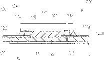
图3是根据本发明的一示范性非限制实施例的COF封装200的平面图。图4是沿图3的IV-IV线得到的横截面图。图5是根据本发明的一示范性非限制实施例的COF封装200的底视图。FIG. 3 is a plan view of a
参照图3至5,COF封装200可以包括带布线基板120和半导体芯片110。带布线基板120可以具有双金属层124和131。半导体芯片110可以被倒装芯片式键合到带布线基板120。模塑料140可密封被倒装芯片式键合的部分。可以经由例如下填充工艺来设置模塑料。Referring to FIGS. 3 to 5 , the
半导体芯片110可以具有带有电极焊盘112的有源表面。电极焊盘112可以沿着有源表面的外围设置。可以在电极焊盘112上设置电极凸点116。电极凸点116可以包括例如输入凸点117和输出凸点118。输入凸点117可以包括例如接地凸点117a和电源凸点(未示出)。输入凸点117可以在尺寸和/或节距上大于输出凸点118。这可以减小例如由于输入凸点117之间的静电所致的故障可能性。半导体芯片110可以包括伪凸点(dummy pattern)119。伪凸点119例如可以设置在有源表面的角部区域。伪凸点119可以改善例如组装稳定性和/或热辐射性。The
带布线基板120可以包括基薄膜121。基薄膜121可以由例如聚酰亚胺制造。基薄膜121也可以由本领域中公知的多种其他材料制成。双金属层124和131可以由例如在基薄膜121上成箔的Cu制造。双金属层124和131也可以由本领域中公知的各种材料(Cu之外)并使用各种技术(铺箔之外)来制造。基薄膜121可以含有包括芯片安装区域的上表面122以及与上表面122相对的下表面123。芯片安装区域可以是上表面122的面对半导体芯片110的区域。也就是说,半导体芯片110可以叠置于上表面122的芯片安装区域之上。通路127可以穿通基薄膜121。双金属层124和131可以包括设置在基薄膜121的上表面122上的上金属层124以及设置在基薄膜121的下表面123上的下金属层131。The substrate with
上金属层124可以设置在芯片安装区域上并且可以连接到电极凸点116。上金属层124可以从芯片安装区域向外延伸。上金属层124可以包括例如输入端子图案125和输出端子图案126。仅作为实例,输入端子图案125可以延伸到相对于半导体芯片110的基薄膜121的一侧,输出端子图案126可以延伸到相对于半导体芯片110的基薄膜121的另一侧。输入端子图案125可以包括连接到接地凸点117a的接地端子图案125a。The
下金属层131可以设置在下表面123的对应于芯片安装区域的区域上。例如,芯片安装区域可以叠置在下金属层131之上。下金属层131可以包括接地层132。接地层132可以通过通路127连接到接地端子图案125a。仅作为实例,接地层132可以至少覆盖芯片安装区域。接地层132可以由例如板状物或网状物制造。接地层132可以提供足够的接地面积从而减小由半导体芯片110发射的电磁波的损耗和/或噪声,由此改善电稳定性。A
将接地端子图案125a连接到接地层132的通路127可以减小对于将接地端子图案125a连接到接地层132的单独布线的需要和/或减小接地路线长度。The via 127 connecting the
上金属层124可以设置在芯片安装区域的外围区域上。在一示范性实施例中,上金属层124可以不覆盖芯片安装区域的中心区域。仅在芯片安装区域的外围区域上(而不在芯片安装区域的中心部分上)设置上金属层124有助于下填充工艺期间模塑料140的流动和/或降低空洞产生的可能性。The
接地层132可以用作辐射例如由半导体芯片110发出的热量的散热器。伪凸点119可以连接到接地层132以改善例如热辐射特性。伪凸点119可以通过伪通路134连接到伪端子图案128。The
在本示范性实施例中,接地层132可以是整体的一件式构造。在可选实施例中,接地层也可以是多件式构造。例如,参照图6,COF封装300可以包括具有第一接地层232a和第二接地层232b的带布线基板200。第一接地凸点217a’可以通过第一通路227a连接到第一接地层232a。第二接地凸点217a”可以通过第二通路227a”连接到第二接地层232b。In the exemplary embodiment, the
仅作为实例,多件式接地层232可以在不同的电压施加到半导体芯片210时生效。例如,当半导体芯片210具有施加了5V电压的模拟电路和施加了1.5V电压的数字电路时,接地层可以被分成用于模拟电路的接地层和用于数字电路的接地层。As an example only, the
在以上示范性实施例中,基薄膜可以仅具有接地层。在可选实施例中,基薄膜可以具有接地层和电源层。In the above exemplary embodiments, the base film may have only the ground layer. In alternative embodiments, the base film may have ground and power layers.
参照图7,COF封装400可以具有包括接地层332和电源层333的下金属层331。接地层332可以与电源层333分开。Referring to FIG. 7 , the COF package 400 may have a lower metal layer 331 including a ground layer 332 and a power layer 333 . The ground layer 332 may be separated from the power layer 333 .
电源层333可以设置在基薄膜321的下表面323上,对应于芯片安装区域。电源端子图案(未示出)可以键合到电源凸点317b。电源端子图案可以通过通路327b连接到电源层333。The power supply layer 333 may be disposed on the lower surface 323 of the base film 321 corresponding to a chip mounting area. A power terminal pattern (not shown) may be bonded to the power bump 317b. The power terminal pattern may be connected to the power layer 333 through the via 327b.
将电源凸点317b连接到电源层333的通路327b可以减少对于将电源凸点317b连接到电源层333的单独布线的需要,和/或减小电源路线长度。Via 327b connecting power bump 317b to power layer 333 may reduce the need for separate wiring connecting power bump 317b to power layer 333 and/or reduce power trace length.
仅作为实例,电源层333可以在不同的电压施加到半导体芯片310上时生效。在该示范性实施例中,电源层333可以设置在接地层332之间。As an example only, the power layer 333 may be active when different voltages are applied to the semiconductor chip 310 . In this exemplary embodiment, a power supply layer 333 may be disposed between the ground layers 332 .
包括接地层和电源层的下金属层可以根据半导体芯片的接地凸点和电源凸点的设置和电压而具有各种布局。The lower metal layer including the ground layer and the power layer may have various layouts according to the arrangement and voltage of the ground bump and the power bump of the semiconductor chip.
参照图8,COF封装500可以具有包括接地层432和电源层433的下金属层431。电源层433可以具有围绕接地层432的环形。在该示范性实施例中,电源层433可以具有方环形状。在可选实施例中,电源层433可以具有弓形环形状(例如,圆环形状)。此外,接地层432和电源层433之间的间隔可以是均匀的(如所示)或者变化的。Referring to FIG. 8 , a COF package 500 may have a lower metal layer 431 including a ground layer 432 and a power layer 433 . The power supply layer 433 may have a ring shape surrounding the ground layer 432 . In this exemplary embodiment, the power supply layer 433 may have a square ring shape. In alternative embodiments, the power layer 433 may have an arcuate ring shape (eg, a donut shape). Additionally, the spacing between ground plane 432 and power plane 433 may be uniform (as shown) or varied.
参照图9,COF封装600可以具有包括接地层532和电源层533的下金属层531。电源层533可以具有字母“C”的形状。电源层533可以包围接地层532。Referring to FIG. 9 , the COF package 600 may have a lower metal layer 531 including a ground layer 532 and a power layer 533 . The power supply layer 533 may have a shape of a letter 'C'. The power layer 533 may surround the ground layer 532 .
参照图10,COF封装700可以具有包括接地层632和电源层633的下金属层631。电源层633可以具有梳形。电源层633可以包围接地层632。Referring to FIG. 10 , the COF package 700 may have a lower metal layer 631 including a ground layer 632 and a power layer 633 . The power supply layer 633 may have a comb shape. The power layer 633 may surround the ground layer 632 .
虽然以上示范性实施例示出了电源层可以包围接地层,但可以理解的是,接地层可以包围电源层。此外,在以上示范性实施例中,下金属层可以具有相同形状的接地层和/或相同形状的电源层。在可选实施例中,给定的下金属层可以具有不同形状的接地层和/或不同形状的电源层。Although the above exemplary embodiments show that the power plane may surround the ground plane, it is understood that the ground plane may surround the power plane. Also, in the above exemplary embodiments, the lower metal layer may have the same shape of the ground layer and/or the same shape of the power supply layer. In alternative embodiments, a given lower metal layer may have a differently shaped ground plane and/or a differently shaped power plane.
尽管已经详细描述了本发明的示范性非限制实施例,但应理解的是,对于本领域技术人员而言显而易见的对于基本发明构思的多种变化和/或改进仍将落入由权利要求限定的本发明的示范性实施例的主旨和范围内。Although exemplary non-limiting embodiments of the present invention have been described in detail, it should be understood that various changes and/or improvements to the basic inventive concept that are obvious to those skilled in the art will still fall within the scope of the claims defined in the claims. within the spirit and scope of the exemplary embodiments of the present invention.
本申请要求于2005年7月18日提交的韩国专利申请No.2005-64789的优先权,其全部内容在此引入作为参考。This application claims priority from Korean Patent Application No. 2005-64789 filed on Jul. 18, 2005, the entire contents of which are hereby incorporated by reference.
Claims (18)
Applications Claiming Priority (2)
| Application Number | Priority Date | Filing Date | Title |
|---|---|---|---|
| KR1020050064789AKR100652519B1 (en) | 2005-07-18 | 2005-07-18 | Tape wiring board with dual metal layer and chip on film package |
| KR64789/05 | 2005-07-18 |
Publications (2)
| Publication Number | Publication Date |
|---|---|
| CN1901179Atrue CN1901179A (en) | 2007-01-24 |
| CN1901179B CN1901179B (en) | 2011-06-08 |
Family
ID=37656997
Family Applications (1)
| Application Number | Title | Priority Date | Filing Date |
|---|---|---|---|
| CN2006100678640AActiveCN1901179B (en) | 2005-07-18 | 2006-03-13 | Tape wiring substrate and chip-on-film package using the same |
Country Status (4)
| Country | Link |
|---|---|
| US (2) | US7420270B2 (en) |
| JP (1) | JP5179014B2 (en) |
| KR (1) | KR100652519B1 (en) |
| CN (1) | CN1901179B (en) |
Cited By (8)
| Publication number | Priority date | Publication date | Assignee | Title |
|---|---|---|---|---|
| CN101996972A (en)* | 2009-08-12 | 2011-03-30 | 索尼公司 | Integrated circuit and conductive tape |
| US8097814B2 (en) | 2008-01-31 | 2012-01-17 | Nitto Denko Corporation | Printed circuit board and method of manufacturing the same |
| US8102664B2 (en) | 2008-01-31 | 2012-01-24 | Nitto Denko Corporation | Printed circuit board and method of manufacturing the same |
| CN103809314A (en)* | 2012-11-13 | 2014-05-21 | 美格纳半导体有限公司 | Flexible printed circuit board, semiconductor package,and method of producing the same |
| CN107046762A (en)* | 2016-01-19 | 2017-08-15 | 硅工厂股份有限公司 | Circuit boards for chip-on-film packaging |
| CN109075567A (en)* | 2016-01-21 | 2018-12-21 | 力特有限公司 | Surface-mounted protective device |
| CN110600446A (en)* | 2018-06-12 | 2019-12-20 | 夏普株式会社 | Tape-shaped wiring board and semiconductor device |
| WO2021258736A1 (en)* | 2020-06-22 | 2021-12-30 | 深圳市全洲自动化设备有限公司 | Cof driving module, cof display module, and methods for manufacturing same |
Families Citing this family (38)
| Publication number | Priority date | Publication date | Assignee | Title |
|---|---|---|---|---|
| KR100652519B1 (en)* | 2005-07-18 | 2006-12-01 | 삼성전자주식회사 | Tape wiring board with dual metal layer and chip on film package |
| KR100788415B1 (en)* | 2006-03-31 | 2007-12-24 | 삼성전자주식회사 | Tape Wiring Substrate with Improved EMI Characteristics and Tape Package Using the Same |
| KR100838244B1 (en)* | 2007-06-22 | 2008-06-17 | 삼성전기주식회사 | Electromagnetic Bandgap Structures and Printed Circuit Boards |
| JP2009016626A (en)* | 2007-07-06 | 2009-01-22 | Panasonic Corp | Semiconductor module device, semiconductor module device manufacturing method, flat panel display device, and plasma display panel |
| JP4588748B2 (en)* | 2007-09-25 | 2010-12-01 | Okiセミコンダクタ株式会社 | COF package |
| JP2009094361A (en)* | 2007-10-10 | 2009-04-30 | Nitto Denko Corp | COF substrate |
| JP4973513B2 (en)* | 2008-01-15 | 2012-07-11 | 日立電線株式会社 | Tape carrier for semiconductor device, method for manufacturing tape carrier for semiconductor device, and semiconductor device |
| JP5095460B2 (en)* | 2008-01-17 | 2012-12-12 | シャープ株式会社 | Semiconductor device and display device |
| JP2009182228A (en) | 2008-01-31 | 2009-08-13 | Nitto Denko Corp | Wiring circuit board and manufacturing method thereof |
| JP5139102B2 (en)* | 2008-02-05 | 2013-02-06 | 日東電工株式会社 | Wiring circuit board and manufacturing method thereof |
| SG155096A1 (en) | 2008-03-03 | 2009-09-30 | Micron Technology Inc | Board-on-chip type substrates with conductive traces in multiple planes, semiconductor device packages including such substrates, and associated methods |
| US8017873B2 (en) | 2008-03-03 | 2011-09-13 | Himax Technologies Limited | Built-in method of thermal dissipation layer for driver IC substrate and structure thereof |
| JP4981744B2 (en) | 2008-05-09 | 2012-07-25 | 日東電工株式会社 | Wiring circuit board and manufacturing method thereof |
| JP5236377B2 (en)* | 2008-07-16 | 2013-07-17 | シャープ株式会社 | Semiconductor device and display device |
| KR101535223B1 (en)* | 2008-08-18 | 2015-07-09 | 삼성전자주식회사 | Tape circuit boards, chip-on-film packages and device assemblies |
| JP2010135230A (en)* | 2008-12-05 | 2010-06-17 | Sanyo Electric Co Ltd | Electronic equipment |
| JP2010206072A (en)* | 2009-03-05 | 2010-09-16 | Hitachi Cable Ltd | Tape carrier for semiconductor device, and semiconductor device |
| JP5325684B2 (en) | 2009-07-15 | 2013-10-23 | ルネサスエレクトロニクス株式会社 | Semiconductor device |
| JP5466966B2 (en)* | 2010-02-16 | 2014-04-09 | 新藤電子工業株式会社 | Wiring board, semiconductor device, semiconductor module, and display device |
| KR101633373B1 (en)* | 2012-01-09 | 2016-06-24 | 삼성전자 주식회사 | COF package and semiconductor comprising the same |
| KR20130096990A (en)* | 2012-02-23 | 2013-09-02 | 삼성전자주식회사 | Semiconductor device |
| KR101900738B1 (en)* | 2012-08-23 | 2018-09-20 | 삼성전자주식회사 | Chip On Film : COF |
| KR101979361B1 (en)* | 2012-10-25 | 2019-05-17 | 삼성디스플레이 주식회사 | Chip on film and display device including the same |
| USD758372S1 (en) | 2013-03-13 | 2016-06-07 | Nagrastar Llc | Smart card interface |
| USD759022S1 (en)* | 2013-03-13 | 2016-06-14 | Nagrastar Llc | Smart card interface |
| KR102107149B1 (en)* | 2013-04-19 | 2020-05-29 | 삼성디스플레이 주식회사 | Cof package and display device including the same |
| KR102081152B1 (en) | 2013-07-24 | 2020-02-26 | 삼성디스플레이 주식회사 | Cof package and display device including the same |
| KR102254761B1 (en) | 2013-09-13 | 2021-05-25 | 삼성디스플레이 주식회사 | Cof package, cof package array including the same, and display device |
| KR102314774B1 (en)* | 2014-11-26 | 2021-10-21 | 삼성전자주식회사 | Semiconductor package |
| USD864968S1 (en)* | 2015-04-30 | 2019-10-29 | Echostar Technologies L.L.C. | Smart card interface |
| KR102059478B1 (en) | 2017-09-15 | 2019-12-26 | 스템코 주식회사 | Printed circuit boards and fabricating method of the same |
| KR102088920B1 (en)* | 2017-12-13 | 2020-03-13 | 주식회사 엘비루셈 | Film for use in COF Package with 2-layer Pattern |
| JP2018085522A (en)* | 2017-12-21 | 2018-05-31 | ルネサスエレクトロニクス株式会社 | Semiconductor device |
| US11259406B2 (en)* | 2018-11-21 | 2022-02-22 | Synaptics Incorporated | Flexible connector for a display device |
| TWI727912B (en)* | 2019-06-19 | 2021-05-11 | 萬潤科技股份有限公司 | Method and equipment for attaching heat-dissipating rubber pad |
| KR102801361B1 (en) | 2020-03-16 | 2025-05-02 | 삼성디스플레이 주식회사 | Display device |
| TWI713178B (en)* | 2020-04-16 | 2020-12-11 | 南茂科技股份有限公司 | Chip-on-film package structure |
| KR20230021204A (en) | 2021-08-04 | 2023-02-14 | 삼성전자주식회사 | Chip On Film Package |
Family Cites Families (23)
| Publication number | Priority date | Publication date | Assignee | Title |
|---|---|---|---|---|
| JP2500785B2 (en) | 1993-09-20 | 1996-05-29 | 日本電気株式会社 | Film carrier tape for semiconductor package and semiconductor device using the same |
| TW407364B (en)* | 1998-03-26 | 2000-10-01 | Toshiba Corp | Memory apparatus, card type memory apparatus, and electronic apparatus |
| JP2000077559A (en) | 1998-08-28 | 2000-03-14 | Toshiba Corp | Semiconductor device |
| JP2000138313A (en)* | 1998-10-30 | 2000-05-16 | Shinko Electric Ind Co Ltd | Semiconductor device and its manufacture |
| JP2000294894A (en)* | 1998-12-21 | 2000-10-20 | Seiko Epson Corp | Circuit board, method of manufacturing the same, and display device and electronic apparatus using the circuit board |
| TW511264B (en) | 1999-02-18 | 2002-11-21 | Seiko Epson Corp | Semiconductor device, mounting substrate and its manufacturing method, circuit substrate and electronic machine |
| JP2001102406A (en) | 1999-09-28 | 2001-04-13 | Toshiba Corp | Area array package and semiconductor device |
| US6580159B1 (en)* | 1999-11-05 | 2003-06-17 | Amkor Technology, Inc. | Integrated circuit device packages and substrates for making the packages |
| JP2001177013A (en) | 1999-12-14 | 2001-06-29 | Matsushita Commun Ind Co Ltd | High-frequency semiconductor device and radio device using device thereof |
| JP2002343899A (en)* | 2001-05-17 | 2002-11-29 | Sharp Corp | Substrate for semiconductor package, semiconductor package |
| JP2003098439A (en)* | 2001-09-25 | 2003-04-03 | Olympus Optical Co Ltd | Microscope capable of changing over observation |
| JP4176979B2 (en)* | 2001-09-27 | 2008-11-05 | パイオニア株式会社 | Flat panel display |
| KR100859804B1 (en) | 2001-11-02 | 2008-09-23 | 엘지디스플레이 주식회사 | Mounting structure and liquid crystal display device using the same |
| JP2004071670A (en) | 2002-08-02 | 2004-03-04 | Fuji Photo Film Co Ltd | Ic package, connecting structure and electronic apparatus |
| JP3871634B2 (en)* | 2002-10-04 | 2007-01-24 | シャープ株式会社 | COF semiconductor device manufacturing method |
| JP3908671B2 (en)* | 2003-01-29 | 2007-04-25 | 松下電器産業株式会社 | Semiconductor device and display device using the same |
| JP4196377B2 (en)* | 2003-09-09 | 2008-12-17 | ソニーケミカル&インフォメーションデバイス株式会社 | Electronic component mounting method |
| JP2005109254A (en)* | 2003-09-30 | 2005-04-21 | Optrex Corp | Integrated circuit mounting substrate and display device equipped with same |
| KR101008973B1 (en)* | 2003-10-11 | 2011-01-17 | 삼성전자주식회사 | Tape wiring board, semiconductor chip package using the same, and liquid crystal display using the same |
| KR100568224B1 (en)* | 2003-11-04 | 2006-04-07 | 삼성전자주식회사 | Tape wiring board and semiconductor device including same |
| JP3943096B2 (en)* | 2004-03-31 | 2007-07-11 | シャープ株式会社 | SEMICONDUCTOR DEVICE, ITS ELECTRIC INSPECTION METHOD, AND ELECTRONIC DEVICE HAVING THE SAME |
| JP4438940B2 (en)* | 2004-05-24 | 2010-03-24 | セイコーエプソン株式会社 | Wiring board, semiconductor device, electronic device and electronic equipment |
| KR100652519B1 (en)* | 2005-07-18 | 2006-12-01 | 삼성전자주식회사 | Tape wiring board with dual metal layer and chip on film package |
- 2005
- 2005-07-18KRKR1020050064789Apatent/KR100652519B1/ennot_activeExpired - Fee Related
- 2006
- 2006-02-28USUS11/362,882patent/US7420270B2/enactiveActive
- 2006-03-13CNCN2006100678640Apatent/CN1901179B/enactiveActive
- 2006-03-17JPJP2006075044Apatent/JP5179014B2/enactiveActive
- 2008
- 2008-08-21USUS12/222,986patent/US7880286B2/enactiveActive
Cited By (13)
| Publication number | Priority date | Publication date | Assignee | Title |
|---|---|---|---|---|
| US8097814B2 (en) | 2008-01-31 | 2012-01-17 | Nitto Denko Corporation | Printed circuit board and method of manufacturing the same |
| US8102664B2 (en) | 2008-01-31 | 2012-01-24 | Nitto Denko Corporation | Printed circuit board and method of manufacturing the same |
| CN101499452B (en)* | 2008-01-31 | 2012-05-16 | 日东电工株式会社 | Printed circuit board and method of manufacturing the same |
| CN101499453B (en)* | 2008-01-31 | 2012-05-16 | 日东电工株式会社 | Printed circuit board and method of manufacturing the same |
| CN101996972A (en)* | 2009-08-12 | 2011-03-30 | 索尼公司 | Integrated circuit and conductive tape |
| CN101996972B (en)* | 2009-08-12 | 2013-03-27 | 索尼公司 | Integrated circuit and conductive tape |
| CN103809314A (en)* | 2012-11-13 | 2014-05-21 | 美格纳半导体有限公司 | Flexible printed circuit board, semiconductor package,and method of producing the same |
| US9332649B2 (en) | 2012-11-13 | 2016-05-03 | Magnachip Semiconductor, Ltd. | Flexible printed circuit board for packaging semiconductor device and method of producing the same |
| CN107046762A (en)* | 2016-01-19 | 2017-08-15 | 硅工厂股份有限公司 | Circuit boards for chip-on-film packaging |
| CN109075567A (en)* | 2016-01-21 | 2018-12-21 | 力特有限公司 | Surface-mounted protective device |
| CN110600446A (en)* | 2018-06-12 | 2019-12-20 | 夏普株式会社 | Tape-shaped wiring board and semiconductor device |
| CN110600446B (en)* | 2018-06-12 | 2021-12-07 | 深圳通锐微电子技术有限公司 | Tape-shaped wiring board and semiconductor device |
| WO2021258736A1 (en)* | 2020-06-22 | 2021-12-30 | 深圳市全洲自动化设备有限公司 | Cof driving module, cof display module, and methods for manufacturing same |
Also Published As
| Publication number | Publication date |
|---|---|
| US20070013056A1 (en) | 2007-01-18 |
| US7420270B2 (en) | 2008-09-02 |
| JP5179014B2 (en) | 2013-04-10 |
| JP2007027682A (en) | 2007-02-01 |
| KR100652519B1 (en) | 2006-12-01 |
| US7880286B2 (en) | 2011-02-01 |
| CN1901179B (en) | 2011-06-08 |
| US20080315437A1 (en) | 2008-12-25 |
Similar Documents
| Publication | Publication Date | Title |
|---|---|---|
| CN1901179A (en) | Tape wiring substrate and chip-on-film package using the same | |
| US8350158B2 (en) | Tape wiring substrates and packages including the same | |
| KR101376257B1 (en) | Semiconductor devices and methods of manufacturing and packaging thereof | |
| US7329597B2 (en) | Semiconductor chip and tab package having the same | |
| US11133262B2 (en) | Semiconductor packages and display devices including the same | |
| KR100788415B1 (en) | Tape Wiring Substrate with Improved EMI Characteristics and Tape Package Using the Same | |
| CN100521172C (en) | Semiconductor device and method of manufacturing the same | |
| US7589421B2 (en) | Heat-radiating semiconductor chip, tape wiring substrate and tape package using the same | |
| CN1945817A (en) | Semiconductor device and manufacturing method thereof | |
| KR20190135322A (en) | Film package and Package module including the same | |
| JP2011176112A (en) | Semiconductor integrated circuit and method of manufacturing the same | |
| KR101166069B1 (en) | Chip-on-film type semiconductor package, and tape circuit board for the same | |
| TWI509756B (en) | Chip-on-film package structure | |
| TW201209940A (en) | Integrated circuit packaging system with leadframe and method of manufacture thereof | |
| CN1149673C (en) | load assembly | |
| CN110277355A (en) | Thin Film Flip Chip Packaging | |
| CN1606160A (en) | Semiconductor device and method for making same, circuit base plate and electronic device | |
| KR20050035043A (en) | Tape circuit substrate, semiconductor chip package using thereof, and liquid crystal display using thereof | |
| US11830803B2 (en) | Chip-on-film package having redistribution pattern between semiconductor chip and connection terminal | |
| US20250096085A1 (en) | Chip on film package and display apparatus including the same | |
| US11013120B2 (en) | Tape wiring board and semiconductor device | |
| JP2007158080A (en) | Semiconductor device | |
| CN2705801Y (en) | Bare Die Pad Layout for LCD Substrates | |
| KR20070039732A (en) | Tape wiring boards with connected dummy wiring patterns and tape packages using them | |
| CN1551341A (en) | Semiconductor device, electronic device, electronic device, and method for manufacturing semiconductor device |
Legal Events
| Date | Code | Title | Description |
|---|---|---|---|
| C06 | Publication | ||
| PB01 | Publication | ||
| C10 | Entry into substantive examination | ||
| SE01 | Entry into force of request for substantive examination | ||
| C14 | Grant of patent or utility model | ||
| GR01 | Patent grant |