CN1900748A - Polarizing film assembly, method of manufacturing the same and display device having the same - Google Patents
Polarizing film assembly, method of manufacturing the same and display device having the sameDownload PDFInfo
- Publication number
- CN1900748A CN1900748ACNA2006101058170ACN200610105817ACN1900748ACN 1900748 ACN1900748 ACN 1900748ACN A2006101058170 ACNA2006101058170 ACN A2006101058170ACN 200610105817 ACN200610105817 ACN 200610105817ACN 1900748 ACN1900748 ACN 1900748A
- Authority
- CN
- China
- Prior art keywords
- layer
- film
- vibration
- speaker
- assembly
- Prior art date
- Legal status (The legal status is an assumption and is not a legal conclusion. Google has not performed a legal analysis and makes no representation as to the accuracy of the status listed.)
- Pending
Links
Images


Classifications
- G—PHYSICS
- G02—OPTICS
- G02F—OPTICAL DEVICES OR ARRANGEMENTS FOR THE CONTROL OF LIGHT BY MODIFICATION OF THE OPTICAL PROPERTIES OF THE MEDIA OF THE ELEMENTS INVOLVED THEREIN; NON-LINEAR OPTICS; FREQUENCY-CHANGING OF LIGHT; OPTICAL LOGIC ELEMENTS; OPTICAL ANALOGUE/DIGITAL CONVERTERS
- G02F1/00—Devices or arrangements for the control of the intensity, colour, phase, polarisation or direction of light arriving from an independent light source, e.g. switching, gating or modulating; Non-linear optics
- G02F1/01—Devices or arrangements for the control of the intensity, colour, phase, polarisation or direction of light arriving from an independent light source, e.g. switching, gating or modulating; Non-linear optics for the control of the intensity, phase, polarisation or colour
- G02F1/13—Devices or arrangements for the control of the intensity, colour, phase, polarisation or direction of light arriving from an independent light source, e.g. switching, gating or modulating; Non-linear optics for the control of the intensity, phase, polarisation or colour based on liquid crystals, e.g. single liquid crystal display cells
- G02F1/133—Constructional arrangements; Operation of liquid crystal cells; Circuit arrangements
- G02F1/1333—Constructional arrangements; Manufacturing methods
- G02F1/1335—Structural association of cells with optical devices, e.g. polarisers or reflectors
- G02F1/133528—Polarisers
- H—ELECTRICITY
- H04—ELECTRIC COMMUNICATION TECHNIQUE
- H04R—LOUDSPEAKERS, MICROPHONES, GRAMOPHONE PICK-UPS OR LIKE ACOUSTIC ELECTROMECHANICAL TRANSDUCERS; DEAF-AID SETS; PUBLIC ADDRESS SYSTEMS
- H04R7/00—Diaphragms for electromechanical transducers; Cones
- H04R7/16—Mounting or tensioning of diaphragms or cones
- G—PHYSICS
- G02—OPTICS
- G02F—OPTICAL DEVICES OR ARRANGEMENTS FOR THE CONTROL OF LIGHT BY MODIFICATION OF THE OPTICAL PROPERTIES OF THE MEDIA OF THE ELEMENTS INVOLVED THEREIN; NON-LINEAR OPTICS; FREQUENCY-CHANGING OF LIGHT; OPTICAL LOGIC ELEMENTS; OPTICAL ANALOGUE/DIGITAL CONVERTERS
- G02F1/00—Devices or arrangements for the control of the intensity, colour, phase, polarisation or direction of light arriving from an independent light source, e.g. switching, gating or modulating; Non-linear optics
- G02F1/01—Devices or arrangements for the control of the intensity, colour, phase, polarisation or direction of light arriving from an independent light source, e.g. switching, gating or modulating; Non-linear optics for the control of the intensity, phase, polarisation or colour
- G02F1/13—Devices or arrangements for the control of the intensity, colour, phase, polarisation or direction of light arriving from an independent light source, e.g. switching, gating or modulating; Non-linear optics for the control of the intensity, phase, polarisation or colour based on liquid crystals, e.g. single liquid crystal display cells
- G02F1/133—Constructional arrangements; Operation of liquid crystal cells; Circuit arrangements
- G02F1/1333—Constructional arrangements; Manufacturing methods
- G02F1/1335—Structural association of cells with optical devices, e.g. polarisers or reflectors
- G02F1/133528—Polarisers
- G02F1/133531—Polarisers characterised by the arrangement of polariser or analyser axes
Landscapes
- Physics & Mathematics (AREA)
- Nonlinear Science (AREA)
- Engineering & Computer Science (AREA)
- Optics & Photonics (AREA)
- Crystallography & Structural Chemistry (AREA)
- General Physics & Mathematics (AREA)
- Chemical & Material Sciences (AREA)
- Mathematical Physics (AREA)
- Multimedia (AREA)
- Acoustics & Sound (AREA)
- Signal Processing (AREA)
- Liquid Crystal (AREA)
- Polarising Elements (AREA)
Abstract
Translated fromChineseDescription
Translated fromChinese技术领域technical field
本发明涉及偏振膜组件、制造偏振膜组件及具有偏振膜组件的显示设备的方法。更具体地,本发明涉及能够改善音质的偏振膜组件、制造所述偏振膜组件及具有所述偏振膜组件的显示设备的方法。The present invention relates to a polarizing film assembly, a method of manufacturing the polarizing film assembly and a display device with the polarizing film assembly. More particularly, the present invention relates to a polarizing film assembly capable of improving sound quality, a method of manufacturing the polarizing film assembly, and a display device having the same.
背景技术Background technique
通常,显示设备包括阴极射线管(“CRT”)显示设备、等离子显示板(“PDP”)显示设备、液晶显示(“LCD”)设备、有机发光显示(“OLED”)设备等。LCD设备具有多种特性,如轻型结构、较小的尺寸、较薄的厚度等,并且已经广泛用于各种领域,如移动通信设备、监视器、电视机等。In general, display devices include cathode ray tube ("CRT") display devices, plasma display panel ("PDP") display devices, liquid crystal display ("LCD") devices, organic light emitting display ("OLED") devices, and the like. LCD devices have various characteristics such as light structure, small size, thin thickness, etc., and have been widely used in various fields such as mobile communication devices, monitors, televisions, and the like.
显示设备包括如电磁扬声器等声音单元。电磁扬声器包括磁铁、线圈、振膜等,因此显示设备具有较大的尺寸和较重的重量。当减小电磁扬声器的尺寸和重量以具有较轻的重量和较小的尺寸时,恶化了电磁扬声器的音质。The display device includes a sound unit such as an electromagnetic speaker. The electromagnetic speaker includes a magnet, a coil, a diaphragm, etc., and thus the display device has a large size and a heavy weight. When the electromagnetic speaker is reduced in size and weight to have a lighter weight and smaller size, the sound quality of the electromagnetic speaker is deteriorated.
发明内容Contents of the invention
本发明的典型实施例提供了一种显示设备,所述显示设备具有较小尺寸的声音单元、轻量结构、以及改进的音质。Exemplary embodiments of the present invention provide a display device having a smaller-sized sound unit, a lightweight structure, and improved sound quality.
本发明的典型实施例提供了一种能够改进音质的偏振膜组件。Exemplary embodiments of the present invention provide a polarizing film assembly capable of improving sound quality.
本发明的典型实施例还提供了一种用于制造上述偏振膜组件的方法。Exemplary embodiments of the present invention also provide a method for manufacturing the above polarizing film assembly.
本发明的典型实施例还提供了一种具有上述偏振膜组件的显示设备。Exemplary embodiments of the present invention also provide a display device having the above polarizing film assembly.
根据本发明的典型实施例的典型偏振膜组件包括偏振膜、扬声器薄膜、振动改进层、以及线路构件。偏振膜包括用于透射在偏振方向上振动的光的偏振层。扬声器薄膜位于偏振膜之上,用于将电信号转变为机械振动以产生声音。振动改进层插入在偏振膜和扬声器薄膜之间,用于改进机械振动。线路构件与扬声器薄膜电连接,用于传输电信号。A typical polarizing film assembly according to an exemplary embodiment of the present invention includes a polarizing film, a speaker film, a vibration improving layer, and a wiring member. The polarizing film includes a polarizing layer for transmitting light vibrating in a polarizing direction. The speaker film sits on top of the polarizing film to convert electrical signals into mechanical vibrations to produce sound. A vibration improving layer is interposed between the polarizing film and the speaker film for improving mechanical vibration. The line member is electrically connected with the speaker film for transmitting electrical signals.
以下提供了制造根据本发明的典型实施例的典型偏振膜组件的典型方法。形成具有偏振层的主膜。在所述主膜上形成振动改进层。将扬声器薄膜粘附到所述振动改进层,以形成第一膜组件。针对显示板的尺寸切割所述第一膜组件。在所述振动改进层的末端部分上,形成与所述扬声器薄膜的第一电极电连接的导电部件。将具有透明导电粘合剂层的透明保护膜粘附到所述扬声器薄膜的第二电极上。形成与所述导电部件电连接的第一线路以及与所述透明导电粘合剂层电连接的第二线路。A typical method of manufacturing a typical polarizing film assembly according to an typical embodiment of the present invention is provided below. A main film having a polarizing layer is formed. A vibration improving layer is formed on the main film. A speaker membrane is adhered to the vibration modifying layer to form a first membrane assembly. The first film assembly is cut for the size of the display panel. On an end portion of the vibration improving layer, a conductive member electrically connected to the first electrode of the speaker film is formed. A transparent protective film with a transparent conductive adhesive layer was adhered to the second electrode of the speaker film. A first line electrically connected to the conductive member and a second line electrically connected to the transparent conductive adhesive layer are formed.
根据本发明的典型实施例的典型显示设备包括显示板、源极驱动部件、栅极驱动部件、声音信号输出部件、以及偏振件。显示板具有源极线、栅极线、以及与所述源极和栅极线电连接的开关元件。源极驱动部件将第一数据信号转换为模拟类型的第二数据信号,并将所述第二数据信号提供到源极线。栅极驱动部件将栅极信号提供到栅极线。声音信号输出部件将第一声音信号转换为第二声音信号,并输出第二声音信号。偏振件位于所述显示板上,所述偏振件透射实质上在偏振方向上振动的光。偏振件根据第二声音信号产生声音。A typical display device according to an exemplary embodiment of the present invention includes a display panel, a source driving part, a gate driving part, an acoustic signal output part, and a polarizer. The display panel has source lines, gate lines, and switching elements electrically connected to the source and gate lines. The source driving part converts the first data signal into an analog type second data signal and supplies the second data signal to the source line. The gate driving part supplies gate signals to gate lines. The sound signal output part converts the first sound signal into a second sound signal and outputs the second sound signal. A polarizer is located on the display panel, the polarizer transmitting light substantially vibrating in a polarization direction. The polarizer generates sound according to the second sound signal.
根据本发明的另一典型实施例的典型显示设备包括显示组件、扬声器薄膜、以及振动改进层。显示组件包括背光组件、板组件、以及容纳容器。背光组件产生光。板组件利用光来显示图像。容纳容器容纳所述背光组件和板组件。扬声器薄膜位于所述显示组件上,用于产生声音。振动改进层插入在所述显示组件和所述扬声器薄膜之间。An exemplary display device according to another exemplary embodiment of the present invention includes a display assembly, a speaker film, and a vibration improving layer. The display assembly includes a backlight assembly, a board assembly, and a receiving container. The backlight assembly generates light. The board assembly utilizes light to display images. The receiving container accommodates the backlight assembly and the panel assembly. A speaker film is located on the display assembly for producing sound. A vibration improving layer is interposed between the display assembly and the speaker film.
根据本发明的另一典型实施例的典型显示设备包括显示组件以及扬声器薄膜。显示组件包括背光组件、板组件、以及容纳容器。背光组件产生光。板组件利用光来显示图像。容纳容器容纳所述背光组件和板组件。扬声器薄膜位于所述显示组件的表面上。扬声器薄膜包括振动改进层,所述振动改进层插入在扬声器薄膜和显示组件之间。An exemplary display device according to another exemplary embodiment of the present invention includes a display assembly and a speaker film. The display assembly includes a backlight assembly, a board assembly, and a receiving container. The backlight assembly generates light. The board assembly utilizes light to display images. The receiving container accommodates the backlight assembly and the panel assembly. A speaker membrane is located on the surface of the display assembly. The speaker film includes a vibration-modifying layer interposed between the speaker film and the display assembly.
根据本发明典型实施例,具有扬声器薄膜的显示设备产生声音。因此,减小了显示设备的尺寸及厚度。According to an exemplary embodiment of the present invention, a display device having a speaker film generates sound. Therefore, the size and thickness of the display device are reduced.
附图说明Description of drawings
通过参考附图描述本发明的典型实施例,本发明的上述和其它优点将变得更为显而易见,其中:The above and other advantages of the present invention will become more apparent by describing exemplary embodiments of the present invention with reference to the accompanying drawings, in which:
图1是示出了根据本发明典型实施例的典型偏振膜组件的截面图;1 is a cross-sectional view illustrating a typical polarizing film assembly according to an exemplary embodiment of the present invention;
图2是示出了根据本发明另一典型实施例的典型偏振膜组件的截面图;2 is a cross-sectional view illustrating a typical polarizing film assembly according to another exemplary embodiment of the present invention;
图3A到3E是示出了制造图1所示的典型偏振膜组件的典型方法的截面图;3A to 3E are cross-sectional views showing a typical method of manufacturing the typical polarizing film assembly shown in FIG. 1;
图4A和4B是示出了形成图1所示的典型振动改进层的典型处理的截面图;4A and 4B are cross-sectional views showing typical processes for forming the typical vibration-improving layer shown in FIG. 1;
图5A和5B是示出了形成根据本发明另一典型实施例的典型振动改进层的典型处理的截面图;5A and 5B are cross-sectional views illustrating an exemplary process of forming an exemplary vibration improving layer according to another exemplary embodiment of the present invention;
图6A和6B是示出了形成根据本发明另一典型实施例的典型振动改进层的典型处理的截面图;6A and 6B are cross-sectional views illustrating an exemplary process of forming an exemplary vibration improving layer according to another exemplary embodiment of the present invention;
图7是示出了根据本发明另一典型实施例的典型振动改进层的截面图;7 is a cross-sectional view illustrating an exemplary vibration improving layer according to another exemplary embodiment of the present invention;
图8是示出了根据本发明另一典型实施例的典型显示板模块的平面图;8 is a plan view illustrating a typical display panel module according to another exemplary embodiment of the present invention;
图9是沿图8所示的线I-I’截取的截面图;Fig. 9 is a sectional view taken along line I-I' shown in Fig. 8;
图10A和10B是示出了光通过图8所示的典型显示板模块的截面图;10A and 10B are cross-sectional views showing light passing through the typical display panel module shown in FIG. 8;
图11是示出了根据本发明的另一典型实施例的典型显示板模块的平面图;11 is a plan view showing a typical display panel module according to another exemplary embodiment of the present invention;
图12是沿图11所示的线II-II’截取的截面图;Fig. 12 is a sectional view taken along line II-II' shown in Fig. 11;
图13是示出了根据本发明另一典型实施例的典型显示设备的方框图;13 is a block diagram illustrating an exemplary display device according to another exemplary embodiment of the present invention;
图14是示出了图13所示的典型声音信号输出部件的方框图;Fig. 14 is a block diagram showing a typical sound signal output part shown in Fig. 13;
图15是示出了根据本发明另一典型实施例的典型显示设备的分解透视图;15 is an exploded perspective view showing a typical display device according to another exemplary embodiment of the present invention;
图16是示出了图15所示的典型显示设备的截面图;FIG. 16 is a cross-sectional view showing a typical display device shown in FIG. 15;
图17是示出了图15所示的典型扬声器薄膜的操作的方框图;Figure 17 is a block diagram illustrating the operation of the exemplary loudspeaker membrane shown in Figure 15;
图18A和18B是示出了形成图15所示的典型振动改进层的典型处理的截面图;18A and 18B are cross-sectional views showing typical processes for forming the typical vibration improving layer shown in FIG. 15;
图19A和19B是示出了根据本发明另一典型实施例形成典型振动改进层的典型处理的截面图;19A and 19B are cross-sectional views illustrating an exemplary process of forming an exemplary vibration-improving layer according to another exemplary embodiment of the present invention;
图20是示出了根据本发明另一典型实施例形成典型振动改进层的典型方法的截面图;20 is a cross-sectional view illustrating an exemplary method of forming an exemplary vibration improving layer according to another exemplary embodiment of the present invention;
图21是示出了根据本发明另一典型实施例的典型显示设备的截面图;21 is a cross-sectional view illustrating an exemplary display device according to another exemplary embodiment of the present invention;
图22是示出了根据本发明另一典型实施例的典型显示设备的分解透视图。FIG. 22 is an exploded perspective view showing an exemplary display device according to another exemplary embodiment of the present invention.
具体实施方式Detailed ways
下文中,将参考附图更为详细地描述本发明,在附图中示出了本发明的实施例。然而,可以不同形式具体实现本发明,并且不应当将本发明视为限于这里所述的实施例。相反地,提供这些实施例,以使此讨论更彻底及完整,并且将向本领域内普通技术人员传达本发明的范围。在附图中,为了清楚,可能夸大了层和区域的大小和相对大小。Hereinafter, the invention will be described in more detail with reference to the accompanying drawings, in which embodiments of the invention are shown. This invention may, however, be embodied in different forms and should not be construed as limited to the embodiments set forth herein. Rather, these embodiments are provided so that this discussion will be thorough and complete, and will convey the scope of the invention to those skilled in the art. In the drawings, the size and relative sizes of layers and regions may be exaggerated for clarity.
应当理解,当提及元件或层位于另一元件或层“之上”、“连接到”或“耦合到”另一元件或层时,可以直接位于另一元件或层上、直接连接到或耦合到另一元件或层,或者可以存在居间元件或层。相反地,当提及元件“直接位于其上”、“直接连接到”或“直接耦合到”另一元件或层时,则不存在居间元件或层。全文中,相同的数字表示相同的元件。这里所使用的术语“和/或”包括关联列出项的一个或多个的任意和全部组合。It will be understood that when an element or layer is referred to as being "on," "connected to" or "coupled to" another element or layer, it can be directly on, directly connected to, or "coupled to" another element or layer. is coupled to another element or layer, or intervening elements or layers may be present. In contrast, when an element is referred to as being "directly on," "directly connected to" or "directly coupled to" another element or layer, there are no intervening elements or layers present. Throughout, like numerals refer to like elements. As used herein, the term "and/or" includes any and all combinations of one or more of the associated listed items.
应当理解,虽然这里使用了术语第一、第二、第三等来描述各种元件、组件、区域、层和/或部分,这些元件、组件、区域、层和/或部分不应当被这些术语限制。这些术语仅用于区分一个元件、组件、区域、层或部分与另一元件、组件、区域、层或部分。因此,可以将下述的第一元件、组件、区域、层或部分称为第二元件、组件、区域、层或部分,而不偏离本发明的技术。It should be understood that although the terms first, second, third, etc. are used herein to describe various elements, components, regions, layers and/or sections, these elements, components, regions, layers and/or sections should not be referred to by these terms. limit. These terms are only used to distinguish one element, component, region, layer or section from another element, component, region, layer or section. Thus, a first element, component, region, layer or section discussed below could be termed a second element, component, region, layer or section, without departing from the teachings of the present invention.
为了易于描述,这里可以使用如“下方”、“之下”、“下部”、“之上”、“上方”等空间相关术语,以描述附图中示出的一个元件或特征与另一元件或特征的关系。应当理解,空间相关术语意欲包含除附图中示出的方向之外的设备在使用或操作上的不同方向。例如,如果附图中的设备是翻转的,则描述为在其它元件或特征“之下”或“下方”的元件则将被确定为在其它元件或特征“之上”的方向。因此,示例术语“之下”可以包括上和下的方向。可以不同地确定设备的方向(旋转90度或以其它方向),并且这里使用的空间相关描述符相应进行解释。For ease of description, spatial relative terms such as "below", "under", "lower", "above", "above" and the like may be used herein to describe the interaction between one element or feature and another element shown in the drawings. or feature relations. It will be understood that the spatially relative terms are intended to encompass different orientations of the device in use or operation in addition to the orientation depicted in the figures. For example, if the device in the figures is turned over, elements described as "below" or "beneath" other elements or features would then be oriented "above" the other elements or features. Thus, the example term "beneath" can encompass both an orientation of above and below. The device may be oriented differently (rotated 90 degrees or at other orientations) and the spatially relative descriptors used herein interpreted accordingly.
这里使用的术语仅是为了描述特定实施例,并且不用于作为对本发明的限制。这里所使用的单数形式“a”、“an”也意欲包括复数形式,除非内容清晰地作出相反地指示。还应当理解,当在本说明书中使用术语“包括”时,术语“包括”指明了规定特征、整数、步骤、操作、元件和/或组件的存在,但是并不排除一个或多个其它特征、整数、步骤、操作、元件、组件及其组合的存在或附加。The terminology used herein is for describing particular embodiments only and is not intended to be limiting of the invention. As used herein, the singular forms "a" and "an" are intended to include the plural unless the content clearly dictates otherwise. It should also be understood that when the term "comprising" is used in this specification, the term "comprising" indicates the presence of specified features, integers, steps, operations, elements and/or components, but does not exclude one or more other features, The presence or addition of integers, steps, operations, elements, components, and combinations thereof.
这里参考作为本发明的理想实施例(以及中间结构)的示意图的截面图描述了本发明实施例。同样地,如制造技术和/或公差的结果导致的与图示的形状的差异是预计的。因此,不应当将本发明实施例视为限于这里所示的特定区域形状,而是包括由于如制造导致的形状上的偏离。例如,典型地,示出为矩形的注入(implanted)区在其边缘处将具有圆形或弧形特征以及/或者倾斜的注入浓度,而不是从注入到非注入区二元改变。相反地,注入所形成的隐埋区可能导致在隐埋区和通过其进行注入的表面之间的区域中的一些注入。因此,图中所示的区域是实际上是示意性的,并且其形状并不用于说明设备的区域的实际形状,并且并不用于限制本发明的范围。Embodiments of the invention are described herein with reference to cross-section illustrations that are schematic illustrations of idealized embodiments (and intermediate structures) of the invention. Likewise, variations from the illustrated shapes are to be expected as a result of manufacturing techniques and/or tolerances. Thus, embodiments of the invention should not be construed as limited to the particular shapes of regions shown herein but are to include deviations in shapes that result, for example, from manufacturing. For example, an implanted region illustrated as a rectangle will, typically, have rounded or arcuate features and/or a sloped implant concentration at its edges rather than a binary change from implanted to non-implanted region. Conversely, a buried region formed by implantation may result in some implantation in the region between the buried region and the surface through which the implantation takes place. Thus, the regions shown in the figures are schematic in nature and their shapes are not intended to illustrate the actual shape of a region of a device and are not intended to limit the scope of the invention.
除非另外进行了定义,这里使用的所有术语(包括技术和科学术语)具有与本发明所属领域内普通技术人员所普遍理解的含义相同的含义。还应当理解,如在通用字典中定义的那些术语应当被解释为具有与其在相关技术的上下文中的含义一致的含义,并且不应当以理想化或过分正式的意思来解释,除非这里非常清楚地进行了定义。Unless otherwise defined, all terms (including technical and scientific terms) used herein have the same meaning as commonly understood by one of ordinary skill in the art to which this invention belongs. It should also be understood that those terms as defined in commonly used dictionaries should be interpreted as having meanings consistent with their meanings in the context of the relevant art, and should not be interpreted in an idealized or overly formal meaning, unless it is very clear here defined.
下文中,将参考附图描述本发明的典型实施例。Hereinafter, typical embodiments of the present invention will be described with reference to the accompanying drawings.
图1是示出了根据本发明典型实施例的偏振膜组件的截面图。FIG. 1 is a cross-sectional view illustrating a polarizing film assembly according to an exemplary embodiment of the present invention.
参考图1,偏振膜组件100包括顺序层叠的透射偏振膜110、振动改进(或活性)层120、扬声器薄膜130、以及保护膜140,以及线路构件151和152。Referring to FIG. 1 , a
透射偏振膜110包括在透射偏振膜110中顺序层叠的压敏粘合剂(“PSA”)层111、第一保护层112、偏振层113、以及第二保护层114,其中,PSA层111设置在偏振膜组件100的外表面上,以及第二保护层114与振动改进层120相邻设置。第一和第二保护层112和114中的每一个可以包括三醋酸纤维素(“TAC”)。偏振层113可以包括聚乙烯醇(“PVA”)。The transmissive
PSA层111包括粘合材料,并且响应外部提供的压力而粘合。可以用于PSA层111的粘合材料的示例包括但不限于:丙烯酸基树脂、橡胶基树脂等。这些可以单独使用也可以其组合的形式使用。PSA层111还可以包括多个控制PSA层111的折射率的粒子。可以用于控制PSA层111的折射率的粒子的示例包括但不限于:锆、石英等。这些可以单独使用也可以其组合的形式使用。The
第一保护层112设置在PSA层111和偏振层113之间。第二保护层114位于与第一保护层112相对的偏振层113之上。第一和第二保护层112、114的每一个包括透明材料。第一和第二保护层112、114的每一个可以包括醋酸纤维基树脂,如TAC。在图1中,第一和第二保护层112、114的每一个包括具有利用碱性离子皂化的皂化表面的TAC膜。The first
偏振层113透射与偏振方向平行的光振动分量,并阻挡与偏振方向垂直的光振动分量。The
振动改进层120形成在第二保护层114上。在图1中,第二保护层114的上部是表面处理过的,以形成振动改进层120,并且振动改进层120改进了扬声器薄膜130的振动。振动改进层120可以包括空气层。可选地,振动改进层120可以包括弹性材料。导电部件121形成在振动改进层120的末端部分上,并且与扬声器薄膜130的第一电极132相连。The
扬声器薄膜130包括夹在第一电极132和第二电极133之间的压电层131。第一电极132形成在压电层131的第一表面上,其中第一电极132设置在振动改进层120和压电层131之间。第二电极133形成在压电层131的与第一表面相对的第二表面上,其中第二电极133设置在保护膜140和压电层131之间。第一电极132实质上可以是板形的,并且实质上可以覆盖压电层131的第一表面的整个表面区域。同样,第二电极133实质上可以是板形的,并且实质上可以覆盖压电层131的第二表面的整个表面区域。The
压电层131将电声音信号变为机械振动,以产生声音。在图1中,压电层131可以包括聚偏氟乙稀(“PVDF”)或其衍生物。这些可以单独使用或以其组合的形式使用。The
可选地,压电层131可以包括聚偏氟乙稀(“PVDF”)和六氟丙烯(“HFP”)的混合物、偏二氟乙烯/三氟乙烯共聚物(“VDF/TrFE”)等。当将电声音信号提供到第一和第二电极132和133时,设置在第一和第二电极132和133之间的压电层131振动,以产生声音。Alternatively, the
可以将透明导电材料设置在压电层131的第一和第二表面上,以形成第一和第二电极132和133。可以用于第一和第二电极132和133的透明导电材料的示例可以包括但不限于:氧化铟锡(“ITO”)、氧化锡(“TO”)、氧化铟锌(“IZO”)、氧化锌(“ZO”)、氧化铟锡锌(“ITZO”)、非晶态氧化铟锡(“a-ITO”)等。这些可以单独使用或者以其组合的形式使用。A transparent conductive material may be disposed on the first and second surfaces of the
保护膜140包括导电粘合剂层141和保护层142。导电粘合剂层141形成在保护层142的后表面上。保护膜140通过导电粘合剂层141粘附到扬声器薄膜130的第二电极133上。保护膜140从扬声器薄膜130的末端部分突出出来。即,保护膜140可以具有比第二电极133的表面区域大的表面区域。The
线路构件151和152包括第一线路151和第二线路152。第一线路151与扬声器薄膜130的第一电极132电连接。第二线路152与扬声器薄膜130的第二电极133电连接。The
第一线路151与和第一电极132相接触的导电部件121电连接。第二线路152与和第二电极133相接触的导电粘合剂层141电连接。通过第一和第二线路151和152,将电声音信号提供到扬声器薄膜130的第一和第二电极132和133。The
图2是示出了根据本发明另一典型实施例的典型偏振膜组件的截面图。FIG. 2 is a cross-sectional view illustrating a typical polarizing film assembly according to another exemplary embodiment of the present invention.
参考图2,偏振膜组件200包括顺序层叠的反射-透射偏振膜210、振动改进(或活性)层220、扬声器薄膜230、以及保护膜240,以及线路构件251和252。Referring to FIG. 2 , the
反射-透射偏振膜210包括在反射-透射偏振膜210中顺序层叠的第一PSA层211、相差层212、第二PSA层213、第一保护层214、偏振层215、以及第二保护层216。第一和第二保护层214和216中的每一个可以包括但不限于TAC。偏振层215可以包括但不限于PVA。The reflective-transmissive
第一和第二PSA层211和213的每一个可以包括粘合材料,并且响应外部提供的压力而粘合。可以用于第一和第二PSA层211和213的每一个的粘合材料的示例包括但不限于:丙烯酸基树脂、橡胶基树脂等。这些可以单独使用也可以其组合的形式使用。第一和第二PSA层211和213的每一个还可以包括多个控制第一和第二PSA层211和213每一个的折射率的粒子。可以用于控制第一和第二PSA层211和213的每一个的折射率的粒子的示例包括但不限于:锆、石英等。这些可以单独使用也可以其组合的形式使用。Each of the first and second PSA layers 211 and 213 may include an adhesive material, and be bonded in response to pressure provided from the outside. Examples of adhesive materials that may be used for each of the first and second PSA layers 211 and 213 include, but are not limited to, acrylic-based resins, rubber-based resins, and the like. These may be used alone or in combination. Each of the first and second PSA layers 211 and 213 may further include a plurality of particles controlling a refractive index of each of the first and second PSA layers 211 and 213 . Examples of particles that may be used to control the refractive index of each of the first and second PSA layers 211 and 213 include, but are not limited to, zirconium, quartz, and the like. These may be used alone or in combination.
第一保护层214设置在第二PSA层213和偏振层215之间。第二保护层216位于与第一保护层214相对的偏振层215之上。第一和第二保护层214和216的每一个包括透明材料。第一和第二保护层214和216的每一个可以包括醋酸纤维基树脂,例如但不限于TAC。The first protective layer 214 is disposed between the second PSA layer 213 and the
偏振层215透射与偏振方向平行的光振动分量,并阻挡与偏振方向垂直的光振动分量。The
相差层212改变光的相位。例如,相差层212可以将线性偏振光变为右或左循环偏振光。可选地,相差层212还可以将右或左循环偏振光变为以相对于偏振膜组件200的纵向约45°或约135°振动的线性偏振光。The
振动改进层220形成在第二保护层216上。在图1中,第二保护层216的上部是表面处理过的,以形成振动改进层220,并且振动改进层220改进了扬声器薄膜230的振动。振动改进层220可以包括空气层。可选地,振动改进层220可以包括弹性材料。导电部件121形成在振动改进层220的末端部分上,并且与扬声器薄膜230的第一电极232电连接。The
扬声器薄膜230包括设置在第一电极232和第二电极233之间的压电层231。第一电极232形成在压电层231的第一表面上,其中第一电极232设置在振动改进层220和压电层231之间。第二电极233形成在压电层231的与第一表面相对的第二表面上,其中第二电极233设置在保护膜240和压电层231之间。第一电极232实质上可以是板形的,并且实质上可以覆盖压电层231的第一表面的整个表面区域。同样,第二电极233实质上可以是板形的,并且实质上可以覆盖压电层231的第二表面的整个表面区域。The
压电层231将电声音信号变为机械振动,以产生声音。在图2中,压电层231可以包括但不限于:PVDF或其衍生物。这些可以单独使用或以其组合的形式使用。The piezoelectric layer 231 changes electrical sound signals into mechanical vibrations to generate sound. In FIG. 2, the piezoelectric layer 231 may include, but is not limited to: PVDF or its derivatives. These may be used alone or in combination thereof.
当将电声音信号提供到第一和第二电极232和233时,压电层231振动,以产生声音。When an electric sound signal is supplied to the first and second electrodes 232 and 233, the piezoelectric layer 231 vibrates to generate sound.
可以将透明导电材料设置在压电层231的第一和第二表面上,以形成第一和第二电极232和233。可以用于第一和第二电极232和233的透明导电材料的示例可以包括但不限于:ITO、TO、IZO、ZO、ITZO、a-ITO等。这些可以单独使用或者以其组合的形式使用。导电粘合剂层241形成在保护层242的后表面上。保护膜240通过导电粘合剂层241粘附到扬声器薄膜230的第二电极233上。保护膜240从扬声器薄膜230的末端部分突出出来。即,保护膜240可以具有比第二电极233的表面区域大的表面区域。A transparent conductive material may be disposed on the first and second surfaces of the piezoelectric layer 231 to form first and second electrodes 232 and 233 . Examples of transparent conductive materials that may be used for the first and second electrodes 232 and 233 may include, but are not limited to, ITO, TO, IZO, ZO, ITZO, a-ITO, and the like. These may be used alone or in combination thereof. A conductive adhesive layer 241 is formed on the rear surface of the protective layer 242 . The protection film 240 is adhered to the second electrode 233 of the
线路构件251和252包括第一线路251和第二线路252。第一线路251与扬声器薄膜230的第一电极232电连接。第二线路252与扬声器薄膜230的第二电极233电连接。The wiring members 251 and 252 include a first wiring 251 and a second wiring 252 . The first wire 251 is electrically connected to the first electrode 232 of the
第一线路251与和第一电极232相接触的导电部件221电连接。第二线路252与和第二电极233相接触的导电粘合剂层241电连接。通过第一和第二线路251和252,将电声音信号提供到扬声器薄膜230的第一和第二电极232和233。The first line 251 is electrically connected to the conductive member 221 in contact with the first electrode 232 . The second wiring 252 is electrically connected to the conductive adhesive layer 241 in contact with the second electrode 233 . The electric sound signal is supplied to the first and second electrodes 232 and 233 of the
图3A到3E是示出了制造图1所示的典型偏振膜组件的典型方法的截面图。3A to 3E are cross-sectional views illustrating a typical method of manufacturing the typical polarizing film assembly shown in FIG. 1 .
参考图1和图3A,利用层压单元对用于形成PSA层111的卷状PSA膜、用于形成第一保护层112的卷状第一保护膜、用于形成偏振层113的卷状偏振膜、用于形成第二保护层114的卷状第二保护膜进行层压,以形成第一偏振件F1。With reference to Fig. 1 and Fig. 3 A, utilize lamination unit to be used for forming the roll-shaped PSA film of
第二保护层114的上部是表面处理过的,以形成偏振改进层120,从而形成第二偏振件F2。振动改进层120增加扬声器薄膜130在透射偏振膜110上的振动量。例如,振动改进层120可以是压花层、空气层、气泡层等。可选地,振动改进层120可以包括具有隔离物(spacer)的透明弹性材料。The upper portion of the second
参考图3B和图3C,扬声器薄膜130粘附到第二偏振件F2上,并位于振动改进层120之上,以形成第三偏振件F3。扬声器薄膜130包括压电层131、形成在压电层131的第一表面上的第一电极132、以及形成在压电层131的第二表面上的第二电极133。Referring to FIGS. 3B and 3C , the
针对显示板的大小,对具有粘附到偏振膜110和振动改进层120上的扬声器薄膜130的第三偏振件F3进行切割,以形成第四偏振件F4。For the size of the display panel, the third polarizer F3 having the
将具有流动性的导电材料注入到振动改进层120的末端部分上的空间中,以形成导电部件121。导电部件121与第一电极132相接触,并且与第一电极132电连接。A conductive material having fluidity is injected into the space on the end portion of the
参考图3D和图3E,将具有导电粘合剂层141和保护层142的保护膜140在扬声器薄膜130的第二电极133处粘附到第四偏振件F4上,以形成第五偏振件F5。3D and 3E, the
导电粘合剂层141与扬声器薄膜130的第二电极133相接触。保护膜140从扬声器薄膜130的与其上导电部件121接触的末端部分相对的末端部分突出出来。The conductive
第一线路151形成在位于扬声器薄膜130的第一末端部分上的导电部件121上,以及第二线路152形成在扬声器薄膜130的第二末端部分上。The
第一和第二线路151和152用作扬声器薄膜130的输入端子。第一和第二线路151和152分别与第一和第二电极132和133电连接。The first and
图4A和4B是示出了形成图1所示的典型振动改进层的典型处理的截面图。4A and 4B are cross-sectional views showing a typical process of forming the typical vibration improving layer shown in FIG. 1 .
参考图1、图4A和图4B,在透射偏振膜110的第二保护层114上涂上合成树脂层321。利用具有压花图案的模子311对合成树脂层321进行压印。Referring to FIGS. 1 , 4A and 4B, a
因此,形成了具有压花图案的振动改进层322。振动改进层322包括多个凸起322a和多个凹陷322b。在凹陷322b中形成空气层。Thus, the
合成树脂层321包括丙烯醛基紫外线固化树脂。可以用于合成树脂层321的丙烯醛基紫外线固化树脂的示例包括但不限于:具有丙烯酸酯、环氧丙烯酸酯、聚酯丙烯酸酯、聚氨酯丙烯酸酯等的光聚合单体或齐聚物、乙酰苯、苯甲酮、噻吨酮等。这些可以单独使用或者以其组合的形式使用。The
图5A和5B是示出了形成根据本发明另一典型实施例的典型振动改进层的典型处理的截面图。5A and 5B are cross-sectional views illustrating an exemplary process of forming an exemplary vibration improving layer according to another exemplary embodiment of the present invention.
参考图1、图5A和图5B,在透射偏振膜110的第二保护层114上涂上合成树脂层323。利用具有开口图案的掩模312,在合成树脂层323上形成图案,以形成振动改进层324。Referring to FIGS. 1 , 5A, and 5B, a
振动改进层324包括多个凸起324a和多个凹陷324b。在凹陷324b中形成空气层。The
合成树脂层323包括丙烯醛基紫外线固化树脂。可以用于合成树脂层323的丙烯醛基紫外线固化树脂的示例包括但不限于:具有丙烯酸酯、环氧丙烯酸酯、聚酯丙烯酸酯、聚氨酯丙烯酸酯等的光聚合单体或齐聚物、乙酰苯、苯甲酮、噻吨酮等。这些可以单独使用或者以其组合的形式使用。The
图6A和6B是示出了形成根据本发明另一典型实施例的典型振动改进层的典型处理的截面图。6A and 6B are cross-sectional views illustrating an exemplary process of forming an exemplary vibration improving layer according to another exemplary embodiment of the present invention.
参考图1、图6A和图6B,在透射偏振膜110的第二保护层114上涂上合成树脂层325。合成树脂层325包括具有在高压下是惰性气体的发泡剂。可以用于发泡剂的惰性气体的示例包括但不限于:二氧化碳、氮等。这些可以单独使用或者以其组合的形式使用。然后,对具有发泡剂的合成树脂层325进行减压并加热,以在合成树脂层325中形成气泡325a。Referring to FIGS. 1 , 6A, and 6B, a synthetic resin layer 325 is coated on the second
因此,在第二保护层114上将合成树脂层325形成为具有气泡325a的振动改进层。Accordingly, the synthetic resin layer 325 is formed as a vibration improving layer having air bubbles 325 a on the second
图7是示出了根据本发明另一典型实施例的典型振动改进层的截面图。FIG. 7 is a cross-sectional view showing an exemplary vibration improving layer according to another exemplary embodiment of the present invention.
参考图7,在透射偏振膜110的第二保护层114上涂上合成树脂层327。合成树脂层327包括多个隔离物327a。例如,合成树脂层327包括透明弹性粘合剂。Referring to FIG. 7, a
隔离物327a保持扬声器薄膜130和透射偏振膜110之间的距离。合成树脂层327的透明弹性粘合剂增加了扬声器薄膜130的振动。合成树脂层327的透明弹性粘合剂实质上可以起与扬声器薄膜130和透射偏振膜110之间的空气层相同的作用,如在之前的典型实施例中所描述的。The
图8是示出了根据本发明另一典型实施例的典型显示板模块的平面图。图9是沿图8所示的线I-I’截取的截面图。FIG. 8 is a plan view illustrating a typical display panel module according to another exemplary embodiment of the present invention. Fig. 9 is a sectional view taken along line I-I' shown in Fig. 8 .
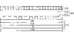
参考图8和图9,显示板模块包括液晶显示(“LCD”)板、用作上偏振件的偏振膜组件200、以及下偏振件201。用作上偏振件的偏振膜组件200位于LCD板的上表面。下偏振件201位于LCD板的下表面。Referring to FIGS. 8 and 9 , the display panel module includes a liquid crystal display (“LCD”) panel, a
LCD板包括阵列衬底450、相对的衬底420、以及液晶层430。相对的衬底420面向阵列衬底450。液晶层430插入在阵列衬底450和相对的衬底420之间。The LCD panel includes an
阵列衬底450包括第一基衬底401以及形成在第一基衬底401上的多条栅极线GLn、多条源极线DLm-1、DLm和DLm+1、多条存储公用线419、以及多个像素P。每个像素P包括开关元件TFT(如薄膜晶体管)、像素电极416、以及反射电极417。像素电极416与开关元件TFT电连接。反射电极417位于像素电极416的用于定义反射区RA的部分上。用像素电极416上不具有反射电极417的部分来限定透射区TA。The
开关元件TFT包括栅极电极411、源极电极413、以及漏极电极414。栅极电极411与栅极线GLn之一电连接。源极电极413与数据线DLm+1之一电连接。漏极电极414与像素电极416电连接。The switching element TFT includes a gate electrode 411 , a
栅极绝缘层402形成在栅极线GLn、栅极电极411、以及存储公用线419上。栅极绝缘层402还可以形成在第一基衬底401的暴露部分上。沟道层412形成在栅极电极411和彼此分离的源极、漏极电极413、414之间的栅极绝缘层402上。沟道层412包括非晶硅层412a和N+非晶硅层412b。在非晶硅层412a的上部注入杂质,以形成N+非晶硅层412b。The
钝化层403形成在数据线DLm+1、源极电极413和漏极电极414上。钝化层403还可以形成在栅极绝缘层402的暴露部分上,以及形成在源极电极413和漏极电极414之间限定的沟道区内的非晶硅层412a上,并通过在N+非晶硅层412b中创建的开口暴露出来。有机层404形成在与反射区RA相对应的钝化层403上。对有机层404的表面形成图案,以具有压花形状,从而有机层404的上部可以用作微反射透镜,漫射外部提供的光。可选地,有机层404还可以具有平面。A
部分地移除漏极电极414上的钝化层403和有机层404,以形成接触孔415,通过接触孔415,漏极电极414部分被暴露出来。The
像素电极416通过接触孔415与漏极电极414电连接。像素电极416包括透明导电材料。可以用于像素电极416的透明导电材料的示例可以包括但不限于:ITO、TO、IZO、ZO、ITZO、a-ITO等。这些可以单独使用或者以其组合的形式使用。The
反射电极417部分形成在像素电极416上,以定义反射区RA。用像素电极416上不具有反射电极417的部分来限定透射区TA。反射电极417包括高反射材料。可以用于反射电极417的高反射材料的示例包括但不限于:铝、铝钕合金、银、银钼合金等。这些可以单独使用或者以其组合的形式使用。The
相对的衬底420包括第二基衬底421。The
黑底(black matrix)422形成在第二基衬底421上。黑底421与阵列衬底450的源极线DLm-1、DLm和DLm+1和栅极线GLn相对应。A black matrix 422 is formed on the
当形成在源极线DLm-1、DLm和DLm+1下的存储公用线419具有足够大覆盖源极线DLm-1、DLm和DLm+1的每一条的尺寸时,黑底422可以仅覆盖栅极线GLn,从而存储公用线419可以起黑底422的作用。When the storage
滤色层423形成在具有黑底422的第二基衬底421上。滤色层423可以包括但不限于红色、绿色、和蓝色滤色器。The
光孔LH可以形成在滤色层423的与反射区RA的部分相对应的部分上。部分地移除滤色层423的部分,以形成光孔LH。外涂层424形成在滤色层423上。公共电极层425形成在外涂层424上。A light hole LH may be formed on a portion of the
液晶层430包括与透射区TA相对应的第一单元间隙2Δnd和与反射区RA相对应的第二单元间隙Δnd,从而反射区RA实质上具有与透射区TA相同的光路径,其中,Δn和d分别表示液晶层430的各向异性和厚度。在图8和9中,有机层404在反射区RA中的厚度比其在透射区TA中的厚度大。如图9所示,可以从透射区TA中排除有机层404。可选地,外涂层424的厚度可以变化以控制单元间隙。The
用于形成图8和9的上偏振件的偏振膜组件200实质上与图2中的相同,并且参考图2,以便更为详细地观察图8和9的显示板模块的上偏振件。因此,相同的参考数字将用于表示与图2中描述的部件相同或相似的部件,以及将省略有关上述元件的详细解释。The
再次参考图2,偏振膜组件200包括反射-透射偏振膜210、振动改进层220、扬声器薄膜230、以及保护膜240,以及线路构件251和252。包括相差层212的反射-透射偏振膜210改变光的相位。例如,反射-透射偏振膜210可以将线性偏振光变为右或左循环偏振光。可选地,反射-透射偏振膜210还可以将右或左循环偏振光变为线性偏振光。Referring again to FIG. 2 , the
线路构件251和252在扬声器薄膜230和声音信号输出部分(未示出)之间电连接,以传输电声音信号。扬声器薄膜230将电声音信号变为机械振动,以产生声音。The line members 251 and 252 are electrically connected between the
振动改进层220插入在反射-透射偏振膜210和扬声器薄膜230之间,以改进声音的音质。The
下偏振件201实质上可以具有与反射-透射偏振膜210相同的材料。例如,下偏振件201可以包括将线性偏振光变为右或左循环偏振光的相差层,如相差层212。可选地,下偏振件201还可以将右或左循环偏振光变为线性偏振光。The
图10A和10B是示出了光通过图8所示的典型显示板模块的截面图。显示板模块具有常时亮态模式。在常时亮态模式下,当未将电功率提供给液晶层430时,显示板模块显示白图像。此外,用作上偏振件的偏振膜组件200部分包括第一偏振层215和第一相差层212。如图10B所示的下偏振件201部分包括第二偏振层205和第二相差层202。10A and 10B are cross-sectional views showing light passing through the typical display panel module shown in FIG. 8 . The display panel module has a always-on mode. In the always-on mode, when electric power is not supplied to the
参考图8到10A,在反射模式下,对应于反射区RA,当未将电功率提供给液晶层430时,外部提供的光通过第一偏振层215,成为线性偏振光。该线性偏振光通过第一相差层212,成为如左循环偏振光。可选地,线性偏振光可以通过第一相差层212,成为右循环偏振光。即,第一相差层212改变光的相位约λ/4。Referring to FIGS. 8 to 10A, in the reflective mode, corresponding to the reflective area RA, when electric power is not supplied to the
当左循环偏振光通过液晶层430时,液晶层430保持水平排列,因为并未向液晶提供电功率,如图10A的OFF模式中所示的。具有水平排列的液晶层430将左循环偏振光变为线性偏振光。即,液晶层430改变光的相位约λ/4。反射的线性偏振光再次通过液晶层430,成为左循环偏振光。液晶层430改变光的相位约λ/4。液晶层430与反射区RA相对应的光特性是约Δnd,表示第二单元间隙(cell gap)。When left circularly polarized light passes through the
左循环偏振光通过第一相差层212,成为线性偏振光,以实质上与第一偏振层215的第一偏振方向平行的方向上振动。线性偏振光通过第一偏振层215,从而显示白图像。The left circularly polarized light passes through the first
在反射模式下,如图10A的ON模式所示,当将电功率提供到液晶层430时,外部提供的光通过第一偏振层215,成为线性偏振光。该线性偏振光通过第一相差层212,成为如左循环偏振光。即,相差层212改变光的相位约λ/4。In the reflective mode, as shown in the ON mode of FIG. 10A, when electric power is supplied to the
左循环偏振光通过由于提供到液晶的电功率而垂直排列的液晶层430,从而左循环偏振光离开液晶层430。即,液晶层430并未改变光的相位,并让左循环偏振光通过液晶层430。从反射电极417反射左循环偏振光,成为右循环偏振光。反射的右循环偏振光通过液晶层430。然后,右循环偏振光通过第一相差层212,成为线性偏振光,在实质上与第一偏振方向垂直的方向上振动。线性偏振光被第一偏振层215阻挡,从而显示黑图像。The left circularly polarized light passes through the
参考图8、9和10B,在透射模式下,对应于透射区TA,如图10B中的OFF模式所示,当未向液晶层430提供电功率时,从背光组件(未示出)产生的内部提供的光通过第二偏振层205,成为线性偏振光。该线性偏振光通过第二相差层202,成为右循环偏振光。即,第二相差层202改变光的相位约λ/4。右循环偏振光通过像素电极416,以将其入射到液晶层430。Referring to FIGS. 8, 9 and 10B, in the transmission mode, corresponding to the transmission area TA, as shown in the OFF mode in FIG. 10B, when no electric power is supplied to the
液晶层430与透射区TA相对应的光特性是约2Δnd,表示第一单元间隙,即是液晶层430与反射区RA相对应的光特性的约两倍。The optical characteristic of the
当未向液晶层430提供电功率时,液晶层430是水平排列的。右循环偏振光通过液晶层430,成为左循环偏振光。即,液晶层430改变光的相位约λ/2。左循环偏振光通过第一相差层212,成为线性偏振光,实质上在第一偏振层215的第一偏振方向上振动。线性偏振光通过第一偏振层215,从而显示白图像。When electric power is not supplied to the
在透射模式下,如图10B中的ON模式所示,当向液晶层430提供电功率时,来自背光组件(未示出)的内部提供的光通过第二偏振层205,成为线性偏振光。该线性偏振光通过第二相差层202,成为右循环偏振光。该右循环偏振光通过像素电极416,以将其入射到液晶层430中。In the transmissive mode, as shown in ON mode in FIG. 10B , when electric power is supplied to the
当向液晶层430提供电功率时,液晶层430是垂直排列的。右循环偏振光通过液晶层430,从而右循环偏振光离开液晶层430。即,液晶层430不改变光的相位。When electric power is supplied to the
右循环偏振光通过第一相差层212,成为线性偏振光,实质上与第一偏振层215的第一偏振方向垂直地振动。线性偏振光被第一偏振层215阻挡,从而显示黑图像。The right circularly polarized light passes through the first
在图8到10B中,显示板模块是反射-透射型的显示板模块。可选地,显示板模块可以是透射型。在图8到10B中,用作上偏振件的偏振膜组件200包括扬声器薄膜230。可选地,下偏振件210可以包括扬声器薄膜230。In FIGS. 8 to 10B, the display panel module is a reflection-transmission type display panel module. Alternatively, the display panel module may be of a transmissive type. In FIGS. 8 to 10B , a
图11是示出了根据本发明的另一典型实施例的典型显示板模块的平面图。图12是沿图11所示的线II-II’截取的截面图。FIG. 11 is a plan view illustrating a typical display panel module according to another exemplary embodiment of the present invention. Fig. 12 is a sectional view taken along line II-II' shown in Fig. 11 .
参考图11和12,显示板模块包括有机发光显示(“OLED”)板和位于OLED板之上的偏振膜组件100。11 and 12, the display panel module includes an organic light emitting display ("OLED") panel and a
OLED板包括基衬底405。基衬底405包括多条源极线DLm、多条栅极线GLn、多条偏压线VLk、以及多个像素P。由源极、栅极和偏压线DLm、GLn和VLk来限定像素P。The OLED panel includes a
每个像素P包括第一开关元件TFT1、第二开关元件TFT2、存储电容器CST、以及有机发光元件EL。Each pixel P includes a first switching element TFT1, a second switching element TFT2, a storage capacitor CST, and an organic light emitting element EL.
第一开关元件TFT1包括第一栅极电极441、第一源极电极443、以及第一漏极电极444。第一栅极电极441与栅极线GLn之一电连接。第一源极电极443与源极线DLm之一电连接。第一漏极电极444与存储电容器CST和第二开关元件TFT2电连接。此外,第一开关元件TFT1还可以包括位于第一源极电极443和第一漏极电极444之间的第一栅极电极441上的第一沟道部分442。第一沟道部分442可以包括非晶硅层和N+非晶硅层(未示出)。The first switching element TFT1 includes a
第二开关元件TFT2包括第二栅极电极451、第二源极电极453、以及第二漏极电极454。第二栅极电极451与第一开关元件TFT1的第一漏极电极444电连接。第二源极电极453与偏压线VLk之一电连接。第二漏极电极454与有机发光元件EL电连接。另外,第二开关元件TFT2还可以包括位于第二源极电极453和第二漏极电极454之间的第二栅极电极451上的第二沟道部分452。第二沟道部分452可以包括非晶硅层452a和N+非晶硅层452b。可以对非晶硅层452a的上部注入杂质,以形成N+非晶硅层452b。第二开关元件TFT2可以是驱动有机发光元件EL的驱动元件。The second switching element TFT2 includes a
存储电容器CST包括第一电极461和第二电极462。第一电极461与第二栅极电极451电连接。第二电极462与偏压线VLk电连接。The storage capacitor CST includes a
有机发光元件EL包括像素电极470、公共电极490(图12中所示)和有机发光层480。像素电极470通过形成在钝化层407中的开口456与第二漏极电极454电连接。有机发光层480插入在像素电极470和公共电极490之间。The organic light emitting element EL includes a
栅极绝缘层406插入在第一和第二栅极电极441和451与第一和第二沟道部分442和452之间。栅极绝缘层406还形成在基衬底405的暴露部分上,以及形成在栅极线GLn和存储电容器CST的第一电极461上。钝化层407形成在第一和第二源极电极443和453以及第一和第二漏极电极444和454上。钝化层407还形成在栅极绝缘层406的暴露部分上,以及形成在数据线DLm和存储电容器的第二电极462上。The
有机发光元件EL的像素电极470形成在具有栅极绝缘层406和钝化层407的基衬底405上。有机发光层480形成在像素电极470上。公共电极490形成在有机发光层480上,并且可以还形成在边沿(bank)层408上。像素电极470可以是有机发光元件EL的阳极。公共电极490可以是有机发光元件EL的阴极。The
有机发光层480的由像素电极470上的边沿层408限定的明亮区中可以包括正电荷注入层、正电荷输送层、发光层、负电荷注入层和负电荷输送层。边沿层408可以根据负型感光耐蚀层来形成,边沿层408的内表面可以相对于基衬底405的表面倾斜。The bright region of the organic
操作上,将栅极信号通过栅极线GLn之一提供到第一开关元件TFT1的第一栅极电极441,因此接通第一开关元件TFT1。然后,将数据信号通过源极线DLm之一提供到第二开关元件TFT2。因此,第二开关元件TFT2被接通,并将数据信号存储在存储电容器CST中。Operationally, a gate signal is supplied to the
当接通第二开关元件TFT2时,根据通过偏压线VLk之一传输的偏压,将数据信号提供到有机发光元件EL。因此,有机发光元件EL产生光。When the second switching element TFT2 is turned on, a data signal is supplied to the organic light emitting element EL according to a bias transmitted through one of the bias lines VLk. Therefore, the organic light emitting element EL generates light.
图11和12的偏振膜组件100实质上与图1所示的相同,并且参考图1,以便更为详细地查看图11和12的显示板模块的偏振膜组件100。因此,相同的参考数字将用于表示与图1中所描述的部分相同或相似的部分,并且将省略有关上述元件的详细解释。The
再次参考图1,偏振膜组件100包括透射偏振膜110、振动改进层120、扬声器薄膜130、以及保护膜140,以及线路构件151和152。透射偏振膜110透射与偏振方向平行的光振动分量,并阻挡与偏振方向垂直的光振动分量。Referring again to FIG. 1 , the
将声音信号提供到在扬声器薄膜130和声音信号输出部件(未示出)的输出端子之间电连接的线路构件151和152。扬声器薄膜130将声音信号变为机械振动以产生声音。The sound signal is supplied to
振动改进层120插入在透射偏振膜110和扬声器薄膜130之间,并改进扬声器薄膜130的振动,从而改进音质。The
图13是示出了根据本发明另一典型实施例的典型显示设备的方框图。FIG. 13 is a block diagram illustrating an exemplary display device according to another exemplary embodiment of the present invention.
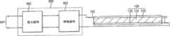
参考图13,显示设备包括定时控制部件510、电压产生部件520、基准伽马电压产生部件530、声音信号输出部件560、以及显示部件570。Referring to FIG. 13 , the display device includes a
定时控制部件510根据从外部单元(未示出)外部提供的控制信号501产生第一控制信号510a、第二控制信号510b、以及第三控制信号510c。第一控制信号510a控制电压产生部件520。第二控制信号510b控制源极驱动部件540。第三控制信号510c控制栅极驱动部件550。The
外部提供的控制信号501可以包括主时钟信号MCLK、水平同步信号HSYNC、垂直同步信号VSYNC、数据使能信号DE等。第一控制信号510a包括主时钟信号MCLK。第二控制信号510b包括水平开始信号STH和加载信号TP。第三控制信号510c包括开始信号STV、扫描时钟信号CPV、以及输出使能信号OE。The externally provided
通过将第二数据信号510d提供到源极驱动部件540的接口方法,定时控制部件510处理来自外部提供单元的第一数据信号502。The
电压产生部件520产生驱动电压以驱动显示设备。更具体地,电压产生部件520产生电源电压520a、栅极电压520b、以及公共电压520c。将电源电压520a提供到基准伽马电压产生部件530。将栅极电压520b提供到栅极驱动部件550。将公共电压520c提供到显示部件570。栅极电压520b包括栅极导通电压和栅极截止电压。公共电压520c包括针对液晶电容器CLC的公共电压VCOM和针对存储电容器CST的公共电压VST。The
基准伽马电压产生部件530包括具有多个与预定伽马曲线相对应的电阻器的电阻器串。利用电阻器串,将从电压产生部件520产生的电源电压520a分为多个基准伽马电压530a,以将基准伽马电压530a提供到源极驱动部件540。The reference gamma
根据第二控制信号510b和基准伽马电压530a,源极驱动部件540将第二数据信号510d转换为模拟类型的第三数据信号,并将模拟类型的第三数据信号提供给显示部件570的源极线DL。According to the
栅极驱动部件550是移位寄存器,根据第三控制信号510c和栅极电压520b,顺序地将多个栅极信号提供给显示部件570的栅极线GL。栅极驱动部件550可以集成在显示部件570上。可选地,栅极驱动部件550可以安装在显示部件570上。The
根据从外部单元提供到声音信号输出部件560的第一声音信号503,声音信号输出部件560将第二声音信号560a提供到显示部件570的偏振膜组件100。更具体地,将第二声音信号560a提供到偏振膜组件100的扬声器薄膜130的两个末端部分。The sound
显示部件570包括LCD板400和位于LCD板400之上的偏振膜组件100。The display part 570 includes the
LCD板400包括源极线DL、栅极线GL、以及以矩阵形式排列的多个像素P。由源极和栅极线DL和GL来限定像素P。每个像素P包括开关元件TFT(如薄膜晶体管)、液晶电容器CLC和存储电容器CST。The
偏振膜组件100包括透射偏振膜110、振动改进层120、扬声器薄膜130、保护膜140、以及线路构件151和152。The
透射偏振膜110包括PSA层111、第一保护层112、偏振层113、以及第二保护层114。第一和第二保护层112和114的每一个可以包括TAC。偏振层113可以包括聚乙烯醇PVA。第一保护层112插入在PSA层111和偏振层113之间。第二保护层114与第一保护层112相对地形成在偏振层113上。The transmissive
偏振层113透射偏振方向上的光振动部分,并阻挡与偏振方向不同方向上的光振动部分。振动改进层120形成在第二保护层114上。振动改进层120可以包括空气层。可选地,振动改进层120可以包括弹性材料。The
扬声器薄膜130包括设置在第一电极132和第二电极133之间的压电层131。第一电极132形成在压电层131的第一表面上,其中第一电极132设置在振动改进层120和压电层131之间。第二电极133形成在压电层131的与第一表面相对的第二表面上,其中第二电极133设置在保护膜140和压电层131之间。第一电极132实质上可以是板形的,并且实质上可以覆盖压电层131的第一表面的整个表面区域。同样,第二电极133实质上可以是板形的,并且实质上可以覆盖压电层131的第二表面的整个表面区域。第一和第二电极132和133分别与第一和第二线路151和152电连接。通过第一和第二线路151和152,将第二声音信号560a提供到扬声器薄膜130。The
图14是示出了图13所示的典型声音信号输出部件的方框图。FIG. 14 is a block diagram showing a typical sound signal output section shown in FIG. 13 .
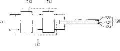
参考图1、13和14,声音信号输出部件560包括输入部件561、放大部件562和转换部件563。转换部件563将第二声音信号560a提供到第一和第二线路151和152,所述第一和第二线路151和152分别与扬声器薄膜130的第一和第二电极132和133电连接。Referring to FIGS. 1 , 13 and 14 , the sound
输入部件561接收从外部源提供到声音信号输出部件560的第一声音信号503。放大部件562放大第一声音信号503的电平。转换部件563根据放大的第一声音信号503输出第二声音信号560a。更具体地,第二声音信号560a驱动扬声器薄膜130。The
通过与转换部件563的输出端子电连接的第一和第二线路151和152,将第二声音信号560a分别提供给第一和第二电极132和133。The
当将第二声音信号560a提供给第一和第二电极132和133时,压电层131振动以产生声音。When the
图15是示出了根据本发明另一典型实施例的典型显示设备的分解透视图。图16是示出了图15所示的典型显示设备的截面图。FIG. 15 is an exploded perspective view showing an exemplary display device according to another exemplary embodiment of the present invention. FIG. 16 is a cross-sectional view showing a typical display device shown in FIG. 15 .
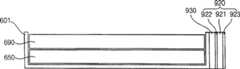
参考图15和16,显示设备包括显示组件600、声音信号输出部件710、扬声器薄膜720、以及振动改进层730。Referring to FIGS. 15 and 16 , the display device includes a
显示组件600包括容纳容器601、背光组件650、以及板组件690。The
容纳容器601包括底板和多个从底板的侧边突出出来以形成容纳空间的侧壁。在容纳容器601的至少一个侧壁上形成固定孔601。The receiving
背光组件650产生光。背光组件650包括光源610、柔性印刷电路板(“PCB”)620、导光板630、以及反射板640。The
光源610产生光。例如,光源610可以包括多个发光二极管(“LED”),但是其它光源也在这些实施例的范围内。光源610可以位于导光板630的一侧上。尽管示出为位于导光板630的一侧上,但是光源610也可以位于导光板630的相对一侧上。The
光源610可以安装在柔性PCB 620上。柔性PCB 620包括电路图案以将驱动信号传输到光源610。可选地,光源610可以与柔性PCB 620分离。The
导光板630对从光源610产生的光进行导向。导光板630可以包括多个点图案(未示出)以引导光。点图案可以印刷在导光板630上。可选地,可以利用形成点图案的模子对印导光板630进行压印。可选地或附加地,诸如凸纹和凹槽等其它图案也可以形成在导光板630上。The
通过位于导光板630之下的反射板640来反射从导光板630泄露出的部分光,以将光反射回导光板630,以增加背光组件650的亮度。反射板640可以是板形、片形等。Part of the light leaked from the
板组件690位于背光组件650上,用于根据光显示图像。板组件690包括模框架660、亮度增加部件670、以及显示板模块680。The
模框架660容纳亮度增加部件670,并引导柔性PCB 620和导光板630。在模框架660的至少一个侧壁上形成固定突起661。The
将固定突起661插入到容纳容器601的固定孔601a中,从而模框架660与容纳容器601结合在一起。因此,将背光组件650固定到容纳容器601。The fixing
亮度增加部件670包括扩散件和多个光片。可以使用任意数量的光片。亮度增加部件670被包括在模框架660中。亮度增加部件670增加了浏览时板上的亮度均匀性和亮度。离开亮度增加部件670的光入射到显示板模块680中。The
显示板模块680利用液晶分子的电和光特性来显示图像。显示板模块680包括显示板683、驱动芯片684、以及柔性PCB 685。The
显示板683包括薄膜晶体管(“TFT”)衬底681、滤色器衬底682、以及包含液晶分子的液晶层(未示出)。滤色器衬底682面向TFT衬底681,并与TFT衬底681组合在一起。液晶层(未示出)插入在TFT衬底681和滤色器衬底682之间。The
驱动芯片684安装在TFT衬底681的外围部分上,用于向显示板683提供驱动信号。驱动信号包括数据信号、栅极控制信号、以及数据控制信号。驱动芯片684可以包括数据驱动芯片和栅极驱动芯片。可选地,驱动芯片684可以包括单个集成驱动芯片。例如,通过玻璃上芯片(“COG”)方法,将驱动芯片684安装在TFT衬底681的外围部分上,但是将驱动芯片684与TFT衬底681组合在一起的其它方法也在这些实施例的范围内。A
将柔性PCB 685安装在TFT衬底681的外围部分上,以向驱动芯片684提供外部提供的信号。柔性PCB 685可以通过各向异性导电膜(“ACF”)与TFT衬底681电连接。A
根据从外部源提供给声音信号输出部件710的第一声音信号,声音信号输出部件710将第二声音信号提供给扬声器薄膜720。The sound
扬声器薄膜720设置在容纳容器601之下,如在容纳容器601的底板之下。扬声器薄膜720包括设置在第一电极722和第二电极723之间的压电层721。第一电极722形成在压电层721的第一表面上。第二电极723形成在压电层721的第二表面上。第一电极722实质上可以是板形的,并且实质上可以覆盖压电层721的第一表面的整个表面区域。同样,第二电极723实质上可以是板形的,并且实质上可以覆盖压电层721的第二表面的整个表面区域。The
压电层721将作为来自声音信号输出部件710的电信号的第二声音信号变为机械振动,以产生声音。压电层721可以包括PVDF及其衍生物。可选地,压电层721可以包括PVDF和HFP的混合物、VDF/TrFE的共聚物等。The
当将从声音信号输出部件710产生的第二声音信号提供给第一和第二电极722和723时,压电层721振动以产生声音。第一和第二电极722和723的每一个可以包括金属或透明导电材料。第一和第二电极722和723位于压电层721的两个相对表面上。When the second sound signal generated from the sound
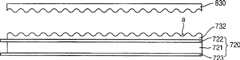
振动改进层730包括空气层、具有多个气泡的气泡层、压花层、弹性透明粘合剂层等中的至少一个,以增加扬声器薄膜720的振动。振动改进层730插入在容纳容器601的一个表面(如底板)和扬声器薄膜720的与容纳容器601的所述一个表面相对应的第一表面之间。例如,振动改进层730可以设置在容纳容器601的底板和扬声器薄膜720的第一电极722之间。The
振动改进层730增加了扬声器薄膜720的第一表面的振动。空气层可以位于扬声器薄膜720的第二表面之上,以增加压电层721的振动。The
图17是示出了图15所示的典型扬声器薄膜的典型操作的方框图。FIG. 17 is a block diagram illustrating a typical operation of the typical speaker membrane shown in FIG. 15 .
参考图17,声音信号输出部件710包括输入部件711、放大部件712和转换部件713。转换部件713将第二声音信号提供到扬声器薄膜720的第一和第二电极722和723。Referring to FIG. 17 , the sound
输入部件711接收从外部源提供到声音信号输出部件710的第一声音信号。放大部件712放大第一声音信号的电平。转换部件713根据放大的第一声音信号输出第二声音信号。更具体地,第二声音信号驱动扬声器薄膜720。The
将从转换部件713的输出端子输出的第二声音信号提供给第一和第二电极722和723。转换部件713的输出端子分别与第一和第二电极722和723电连接。The second sound signal output from the output terminal of the
当将第二声音信号提供给第一和第二电极722和723时,扬声器薄膜720的压电层721振动以产生声音。When the second sound signal is supplied to the first and
图18A和18B是示出了形成图15所示的典型振动改进层的典型处理的截面图。18A and 18B are sectional views showing typical processes of forming the typical vibration improving layer shown in FIG. 15 .
参考图18A和18B,在扬声器薄膜720的第一电极722上涂上合成树脂层731。Referring to FIGS. 18A and 18B, a
利用具有压花图案的模子830对合成树脂层731进行压印,以形成具有压花图案的振动改进层732。The
合成树脂层731包括丙烯醛基紫外线固化树脂。可以用于合成树脂层731的丙烯醛基紫外线固化树脂的示例包括但不限于:具有丙烯酸酯、环氧丙烯酸酯、聚酯丙烯酸酯、聚氨酯丙烯酸酯等的光聚合单体或齐聚物、乙酰苯、苯甲酮、噻吨酮等。这些可以单独使用或者以其组合的形式使用。The
因此,振动改进层732具有多个凸起和多个凹陷。在凹陷中形成空气层,如图18B中参考字符“a”所示。Therefore, the
图19A和19B是示出了形成根据本发明的另一典型实施例的典型振动改进层的典型处理的截面图。19A and 19B are cross-sectional views illustrating an exemplary process of forming an exemplary vibration improving layer according to another exemplary embodiment of the present invention.
参考图19A和19B,在扬声器薄膜720的第一电极722上涂上合成树脂层741。利用具有开口图案的掩模840在合成树脂层741上形成图案,以部分去除合成树脂层741。Referring to FIGS. 19A and 19B, a synthetic resin layer 741 is coated on the
振动改进层742包括多个凸起和多个凹陷。合成树脂层741的部分合成树脂可以保留在振动改进层742中,以形成凸起,并且从振动改进层742中去除合成树脂层741的合成树脂,以形成凹陷。在凹陷中形成空气层,如图19B中参考字符“a”所示。The
合成树脂层741包括丙烯醛基紫外线固化树脂。可以用于合成树脂层741的丙烯醛基紫外线固化树脂的示例包括但不限于:具有丙烯酸酯、环氧丙烯酸酯、聚酯丙烯酸酯、聚氨酯丙烯酸酯等的光聚合单体或齐聚物、乙酰苯、苯甲酮、噻吨酮等。这些可以单独使用或者以其组合的形式使用。The synthetic resin layer 741 includes an acryl-based ultraviolet curable resin. Examples of acryl-based ultraviolet curable resins that can be used for the synthetic resin layer 741 include, but are not limited to, photopolymerizable monomers or oligomers with acrylate, epoxy acrylate, polyester acrylate, urethane acrylate, etc., acetyl Benzene, benzophenone, thioxanthone, etc. These may be used alone or in combination thereof.
图20是示出了形成根据本发明另一典型实施例的典型振动改进层的典型方法的截面图。FIG. 20 is a cross-sectional view illustrating an exemplary method of forming an exemplary vibration improving layer according to another exemplary embodiment of the present invention.
参考图20,在扬声器薄膜720的第一电极722上涂上透明粘合剂752和多个隔离物751的混合物,以形成振动改进层753。透明粘合剂752是可以与扬声器薄膜720的振动同步的弹性材料。Referring to FIG. 20 , a mixture of a transparent adhesive 752 and a plurality of spacers 751 is coated on the
即,隔离物751保持扬声器薄膜720和显示设备之间的距离。弹性材料的透明粘合剂752增加扬声器薄膜720的振动。That is, the spacer 751 maintains the distance between the
图21是示出了根据本发明另一典型实施例的典型显示设备的截面图。除了扬声器薄膜920和振动改进层930之外,图21的显示设备实质上与图15所示的相同。因此,使用相同的参考数字表示与图15中的部件相同或相似的部件,并省略了关于上述元件的详细解释。FIG. 21 is a cross-sectional view illustrating an exemplary display device according to another exemplary embodiment of the present invention. The display device of FIG. 21 is substantially the same as that shown in FIG. 15 except for the
参考图21,显示设备包括显示组件、声音信号输出部件(未示出)、扬声器薄膜920、以及振动改进层930。显示组件部分包括容纳容器601、背光组件650、以及板组件690。Referring to FIG. 21 , the display device includes a display assembly, a sound signal output part (not shown), a
容纳容器601包括用于容纳背光组件650和板组件690的容纳空间。背光组件650产生提供给板组件690的光。板组件690根据光来显示图像。The receiving
扬声器薄膜920位于容纳容器601的侧表面上。例如,扬声器薄膜920位于与容纳容器601的侧壁之一相邻的位置,而不是如上述先前实施例那样位于容纳容器601的底板之下。The
扬声器薄膜920包括设置在第一电极922和第二电极923之间的压电层921。第一电极922形成在压电层921的第一表面上。第二电极923形成在压电层921的第二表面上。第一电极922可以位于比第二电极923更接近于容纳容器601的侧壁的位置。第一和第二电极922、923实质上可以是板形的,并且实质上可以具有与压电层921相同的表面积。The
压电层921将从声音信号输出部件(未示出)输出的第二声音信号变为机械振动,以产生声音。压电层921可以包括但不限于PVDF或其衍生物。The
当将从声音信号输出部件(未示出)产生的第二声音信号提供给第一和第二电极922和923时,压电层921振动以产生声音。第一和第二电极922和923的每一个可以包括金属或透明导电材料。第一和第二电极922和923分别位于压电层921的第一和第二表面上。When a second sound signal generated from a sound signal output part (not shown) is supplied to the first and
振动改进层930包括空气层、具有多个气泡的气泡层、压花层、具有隔离物的弹性透明粘合剂层等中的至少一个,以增加扬声器薄膜920的振动。振动改进层930插入在显示设备的侧表面和扬声器薄膜920之间。更具体地,振动改进层930可以设置在容纳容器601的侧壁和扬声器薄膜920的第一电极922之间。The
振动改进层930增加了扬声器薄膜920的第一表面的振动。空气层可以位于扬声器薄膜920的第二表面之上,以增加压电层921的振动。The
图22是示出了根据本发明的另一典型实施例的典型显示设备的分解透视图。除了扬声器薄膜和振动改进层之外,图22的显示设备实质上与图15所示的相同。因此,使用相同的参考数字表示与图15中所述的部件相同或相似的部分,并且将省略有关上述元件的任何详细解释。FIG. 22 is an exploded perspective view showing an exemplary display device according to another exemplary embodiment of the present invention. The display device of FIG. 22 is substantially the same as that shown in FIG. 15 except for the speaker film and the vibration improving layer. Therefore, the same or similar parts as those described in FIG. 15 are denoted by the same reference numerals, and any detailed explanation about the above elements will be omitted.
参考图22,显示设备包括显示组件600、声音信号输出部件950、扬声器薄膜960、以及振动改进层970。显示组件600包括容纳容器601、背光组件650、以及板组件690。Referring to FIG. 22 , the display device includes a
根据从外部源提供到声音信号输出部件950的第一声音信号,声音信号输出部件950将第二声音信号提供到扬声器薄膜960。The sound
扬声器薄膜960位于显示板683之上。扬声器薄膜960包括设置在第一电极962和第二电极963之间的压电层961。第一电极962形成在压电层961的第一表面上。第二电极963形成在压电层961的第二表面上。第一和第二电极962、963实质上可以是板形的,并且实质上可以具有与压电层961相同的表面积。The
压电层961将从声音信号输出部件950输出的第二声音信号变为机械振动,以产生声音。压电层961可以包括PVDF或其衍生物。可选地,压电层961可以包括但不限于:PVDF和HFP的混合物、VDF/TrFE的共聚物等The
当将从声音信号输出部件950产生的第二声音信号提供给第一和第二电极962和963时,压电层961振动以产生声音。第一和第二电极962和963的每一个可以包括透明导电材料。可以用于第一和第二电极962和963的透明导电材料的示例包括但不限于:ITO、TO、IZO、ZO、ITZO、a-ITO等。这些可以单独使用或以其组合的形式使用。When the second sound signal generated from the sound
振动改进层970包括空气层、具有多个气泡的气泡层、压花层、弹性透明粘合剂层等中的至少一个,以增加扬声器薄膜960的振动。振动改进层970插入在显示板683的一个表面和扬声器薄膜960的与显示板683相对应的第一表面之间。更具体地,振动改进层970可以设置在显示板683的滤色器衬底682和扬声器薄膜960的第一电极962之间。例如,振动改进层970包括透明材料。The
振动改进层970增加了扬声器薄膜960的第一表面的振动。空气层可以位于扬声器薄膜960的第二表面之上,以增加扬声器薄膜960的振动。The
根据本发明,偏振件包括扬声器薄膜,从而显示设备可以产生声音。通过插入在偏振膜和扬声器薄膜之间的用于增加扬声器薄膜的振动的振动改进层,将偏振膜与扬声器薄膜结合在一起,从而增强了音质。因此,可以减小显示设备的尺寸和厚度。According to the present invention, the polarizer includes a speaker film so that the display device can generate sound. The sound quality is enhanced by combining the polarizing film with the speaker film by interposing a vibration-improving layer for increasing the vibration of the speaker film between the polarizing film and the speaker film. Therefore, the size and thickness of the display device can be reduced.
另外,可以利用振动改进层将扬声器薄膜粘附到显示板组件,从而减小了显示设备的尺寸和厚度。此外,增强了音量和音质。In addition, the speaker film can be adhered to the display panel assembly using the vibration improving layer, thereby reducing the size and thickness of the display device. In addition, volume and sound quality have been enhanced.
已经参考典型实施例描述了本发明。然而,显然,按照前面的描述,对本领域内普通技术人员而言许多可选修改和变更将是显而易见的。因此,本发明包含所有落入所附权利要求的精神和范围内的这种可选修改和变更。The invention has been described with reference to the exemplary embodiments. It is evident, however, that many alternative modifications and variations will be apparent to those of ordinary skill in the art in view of the foregoing description. Accordingly, the present invention embraces all such optional modifications and changes as fall within the spirit and scope of the appended claims.
Claims (31)
Translated fromChineseApplications Claiming Priority (3)
| Application Number | Priority Date | Filing Date | Title |
|---|---|---|---|
| KR1020050065293AKR20070010573A (en) | 2005-07-19 | 2005-07-19 | Hybrid polarizing film and a manufacturing method thereof, and a display device having the same |
| KR200565299 | 2005-07-19 | ||
| KR200565293 | 2005-07-19 |
Publications (1)
| Publication Number | Publication Date |
|---|---|
| CN1900748Atrue CN1900748A (en) | 2007-01-24 |
Family
ID=37656672
Family Applications (1)
| Application Number | Title | Priority Date | Filing Date |
|---|---|---|---|
| CNA2006101058170APendingCN1900748A (en) | 2005-07-19 | 2006-07-12 | Polarizing film assembly, method of manufacturing the same and display device having the same |
Country Status (2)
| Country | Link |
|---|---|
| KR (1) | KR20070010573A (en) |
| CN (1) | CN1900748A (en) |
Cited By (10)
| Publication number | Priority date | Publication date | Assignee | Title |
|---|---|---|---|---|
| CN103135161A (en)* | 2011-12-01 | 2013-06-05 | 第一毛织株式会社 | Optical adhesive, optical adhesive and display apparatus comprising the same |
| CN104143292A (en)* | 2013-05-07 | 2014-11-12 | 三星显示有限公司 | display device |
| CN105101695A (en)* | 2014-05-07 | 2015-11-25 | 朱德义 | Protective housing for electronic device and method for transmitting sound in an airtight environment |
| CN107295447A (en)* | 2016-04-05 | 2017-10-24 | 乐金显示有限公司 | Organic Light Emitting Display Device |
| CN109994060A (en)* | 2017-12-29 | 2019-07-09 | 乐金显示有限公司 | display device |
| US10412500B2 (en) | 2016-03-28 | 2019-09-10 | Lg Display Co., Ltd. | Actuator fixing device and panel vibration type sound-generating display device including the same |
| CN110275348A (en)* | 2018-03-15 | 2019-09-24 | 京东方科技集团股份有限公司 | Backlight module and display device |
| CN115083289A (en)* | 2018-09-20 | 2022-09-20 | 乐金显示有限公司 | Display device and computing device including the display device |
| CN115171573A (en)* | 2019-03-29 | 2022-10-11 | 乐金显示有限公司 | Display device |
| CN115278131A (en)* | 2018-12-20 | 2022-11-01 | 乐金显示有限公司 | Equipment with vibrating plate |
Families Citing this family (4)
| Publication number | Priority date | Publication date | Assignee | Title |
|---|---|---|---|---|
| KR100934957B1 (en)* | 2008-02-22 | 2010-01-06 | 한국과학기술연구원 | Hybrid electric device using piezoelectric polymer substrate and its manufacturing method |
| KR102229137B1 (en)* | 2014-05-20 | 2021-03-18 | 삼성디스플레이 주식회사 | Display apparatus |
| KR102778626B1 (en) | 2019-09-04 | 2025-03-12 | 삼성디스플레이 주식회사 | Display device and method of manufacturing display device |
| KR102777157B1 (en) | 2019-12-30 | 2025-03-05 | 엘지디스플레이 주식회사 | Display Device |
- 2005
- 2005-07-19KRKR1020050065293Apatent/KR20070010573A/ennot_activeCeased
- 2006
- 2006-07-12CNCNA2006101058170Apatent/CN1900748A/enactivePending
Cited By (32)
| Publication number | Priority date | Publication date | Assignee | Title |
|---|---|---|---|---|
| US9296929B2 (en) | 2011-12-01 | 2016-03-29 | Cheil Industries, Inc. | Optical member and display apparatus including the same |
| CN103135161A (en)* | 2011-12-01 | 2013-06-05 | 第一毛织株式会社 | Optical adhesive, optical adhesive and display apparatus comprising the same |
| CN103135161B (en)* | 2011-12-01 | 2015-06-17 | 第一毛织株式会社 | Optical adhesive, optical adhesive and display apparatus comprising the same |
| US10735571B2 (en) | 2013-05-07 | 2020-08-04 | Samsung Display Co., Ltd. | Display device |
| CN104143292A (en)* | 2013-05-07 | 2014-11-12 | 三星显示有限公司 | display device |
| US10205810B2 (en) | 2013-05-07 | 2019-02-12 | Samsung Display Co., Ltd. | Display device |
| CN104143292B (en)* | 2013-05-07 | 2019-06-28 | 三星显示有限公司 | Display device |
| US11388278B2 (en) | 2013-05-07 | 2022-07-12 | Samsung Display Co., Ltd. | Display device |
| CN105101695A (en)* | 2014-05-07 | 2015-11-25 | 朱德义 | Protective housing for electronic device and method for transmitting sound in an airtight environment |
| US10841699B2 (en) | 2016-03-28 | 2020-11-17 | Lg Display Co., Ltd. | Panel vibration type display device for generating sound |
| US10547945B2 (en) | 2016-03-28 | 2020-01-28 | Lg Display Co., Ltd. | Panel vibration type sound generating display device |
| US11140482B2 (en) | 2016-03-28 | 2021-10-05 | Lg Display Co., Ltd. | Actuator fixing device and panel vibration type sound-generating display device including the same |
| US10412500B2 (en) | 2016-03-28 | 2019-09-10 | Lg Display Co., Ltd. | Actuator fixing device and panel vibration type sound-generating display device including the same |
| US11950068B2 (en) | 2016-03-28 | 2024-04-02 | Lg Display Co., Ltd. | Panel vibration type sound generating display device |
| US11265655B2 (en) | 2016-03-28 | 2022-03-01 | Lg Display Co., Ltd | Panel vibration type sound generating display device |
| CN113207069B (en)* | 2016-04-05 | 2022-12-30 | 乐金显示有限公司 | Organic light emitting display device |
| US10847585B2 (en) | 2016-04-05 | 2020-11-24 | Lg Display Co., Ltd. | Organic light emitting display device including a sound generating apparatus |
| CN107295447A (en)* | 2016-04-05 | 2017-10-24 | 乐金显示有限公司 | Organic Light Emitting Display Device |
| CN113207069A (en)* | 2016-04-05 | 2021-08-03 | 乐金显示有限公司 | Organic light emitting display device |
| US11012769B2 (en) | 2017-12-29 | 2021-05-18 | Lg Display Co., Ltd. | Display apparatus |
| US11012768B2 (en) | 2017-12-29 | 2021-05-18 | Lg Display Co., Ltd. | Display apparatus |
| US11477554B2 (en) | 2017-12-29 | 2022-10-18 | Lg Display Co., Ltd. | Display apparatus |
| US11785368B2 (en) | 2017-12-29 | 2023-10-10 | Lg Display Co., Ltd. | Display apparatus |
| CN109994060A (en)* | 2017-12-29 | 2019-07-09 | 乐金显示有限公司 | display device |
| US12088982B2 (en) | 2017-12-29 | 2024-09-10 | Lg Display Co., Ltd. | Display apparatus |
| US10939213B2 (en) | 2018-03-15 | 2021-03-02 | Beijing Boe Display Technology Co., Ltd. | Backlight assembly, manufacturing method thereof and display device |
| CN110275348A (en)* | 2018-03-15 | 2019-09-24 | 京东方科技集团股份有限公司 | Backlight module and display device |
| CN115083289A (en)* | 2018-09-20 | 2022-09-20 | 乐金显示有限公司 | Display device and computing device including the display device |
| CN115083289B (en)* | 2018-09-20 | 2024-02-09 | 乐金显示有限公司 | Display devices and computing devices including the display devices |
| CN115278131A (en)* | 2018-12-20 | 2022-11-01 | 乐金显示有限公司 | Equipment with vibrating plate |
| CN115171573A (en)* | 2019-03-29 | 2022-10-11 | 乐金显示有限公司 | Display device |
| CN115171573B (en)* | 2019-03-29 | 2025-07-18 | 乐金显示有限公司 | Display Devices |
Also Published As
| Publication number | Publication date |
|---|---|
| KR20070010573A (en) | 2007-01-24 |
Similar Documents
| Publication | Publication Date | Title |
|---|---|---|
| CN1900748A (en) | Polarizing film assembly, method of manufacturing the same and display device having the same | |
| CN200944140Y (en) | Straight waveguide display panel | |
| CN1134698C (en) | Display and electronic device comprising the same | |
| CN1191489C (en) | Photoelectric device and electronic device | |
| CN1204542C (en) | Photoelectric device, IC for driving and electronic equipment | |
| CN1179230C (en) | Liquid crystal display device having a plurality of pixel electrodes | |
| CN1199073C (en) | Liquid crystal display device | |
| CN1277145C (en) | Display backlight unit and liquid crystal display using same | |
| CN101042492A (en) | Display device | |
| US20070019134A1 (en) | Polarizing film assembly, method of manufacturing the same and display device having the same | |
| CN1991494A (en) | Liquid crystal display device and display device | |
| CN1643439A (en) | Light modulation display device, manufacturing method thereof, and display device equipped with the light modulation display device | |
| CN1773348A (en) | Optical module and manufacturing method thereof, backlight assembly and display device | |
| CN1234878A (en) | Liquid crystal display device | |
| CN1530711A (en) | Backlight assembly, liquid crystal display device, and apparatus for forming a particle stopper | |
| CN101040211A (en) | Composite diffuser plates and direct-lit liquid crystal displays using the same | |
| CN1853068A (en) | Backlight device and liquid crystal display | |
| CN1991506A (en) | Display device | |
| CN1841138A (en) | Electro-optical device, mounting method of wiring substrate, and electronic device | |
| CN1816269A (en) | Display device | |
| CN1646974A (en) | Backlight assembly for liquid crystal display apparatus | |
| CN1922539A (en) | Display apparatus and electronic device | |
| CN1550844A (en) | Electro-optic device, electronic device, and method for manufacturing electro-optic device | |
| CN1769966A (en) | Electro-optic devices and electronics | |
| CN101075037A (en) | Display device |
Legal Events
| Date | Code | Title | Description |
|---|---|---|---|
| C06 | Publication | ||
| PB01 | Publication | ||
| C10 | Entry into substantive examination | ||
| SE01 | Entry into force of request for substantive examination | ||
| C02 | Deemed withdrawal of patent application after publication (patent law 2001) | ||
| WD01 | Invention patent application deemed withdrawn after publication |