CN1897784B - Reducing electrostatic charge by roughening the susceptor - Google Patents
Reducing electrostatic charge by roughening the susceptorDownload PDFInfo
- Publication number
- CN1897784B CN1897784BCN2006100985827ACN200610098582ACN1897784BCN 1897784 BCN1897784 BCN 1897784BCN 2006100985827 ACN2006100985827 ACN 2006100985827ACN 200610098582 ACN200610098582 ACN 200610098582ACN 1897784 BCN1897784 BCN 1897784B
- Authority
- CN
- China
- Prior art keywords
- substrate support
- substrate
- microinches
- coating
- conductor
- Prior art date
- Legal status (The legal status is an assumption and is not a legal conclusion. Google has not performed a legal analysis and makes no representation as to the accuracy of the status listed.)
- Active
Links
- 238000007788rougheningMethods0.000titledescription3
- 239000000758substrateSubstances0.000claimsabstractdescription285
- 238000000576coating methodMethods0.000claimsabstractdescription50
- 239000011248coating agentSubstances0.000claimsabstractdescription47
- 229910052782aluminiumInorganic materials0.000claimsabstractdescription34
- XAGFODPZIPBFFR-UHFFFAOYSA-NaluminiumChemical compound[Al]XAGFODPZIPBFFR-UHFFFAOYSA-N0.000claimsabstractdescription34
- 239000004020conductorSubstances0.000claimsabstractdescription32
- 238000000034methodMethods0.000claimsdescription54
- 230000008569processEffects0.000claimsdescription40
- 230000003746surface roughnessEffects0.000claimsdescription27
- 238000010438heat treatmentMethods0.000claimsdescription21
- 238000012545processingMethods0.000claimsdescription15
- 238000005422blastingMethods0.000claimsdescription11
- 238000005520cutting processMethods0.000claimsdescription11
- 238000004049embossingMethods0.000claimsdescription11
- 239000011324beadSubstances0.000claimsdescription10
- 238000003801millingMethods0.000claimsdescription9
- PNEYBMLMFCGWSK-UHFFFAOYSA-Naluminium oxideInorganic materials[O-2].[O-2].[O-2].[Al+3].[Al+3]PNEYBMLMFCGWSK-UHFFFAOYSA-N0.000claimsdescription7
- 238000005530etchingMethods0.000claimsdescription7
- 238000007743anodisingMethods0.000claimsdescription3
- 238000000227grindingMethods0.000claimsdescription2
- 238000004381surface treatmentMethods0.000claims1
- 238000004519manufacturing processMethods0.000abstractdescription20
- 239000000463materialSubstances0.000description26
- 230000008021depositionEffects0.000description13
- 239000010408filmSubstances0.000description13
- 238000000151depositionMethods0.000description12
- 239000011521glassSubstances0.000description12
- 229910052751metalInorganic materials0.000description10
- 239000002184metalSubstances0.000description10
- 230000036961partial effectEffects0.000description9
- 238000000623plasma-assisted chemical vapour depositionMethods0.000description9
- 239000007789gasSubstances0.000description8
- 230000002787reinforcementEffects0.000description8
- 239000004065semiconductorSubstances0.000description8
- 238000009826distributionMethods0.000description7
- 239000002245particleSubstances0.000description7
- 238000005498polishingMethods0.000description7
- 230000032683agingEffects0.000description5
- 229910052710siliconInorganic materials0.000description5
- 239000010703siliconSubstances0.000description5
- VYPSYNLAJGMNEJ-UHFFFAOYSA-NSilicium dioxideChemical compoundO=[Si]=OVYPSYNLAJGMNEJ-UHFFFAOYSA-N0.000description4
- 239000000919ceramicSubstances0.000description4
- 230000007547defectEffects0.000description4
- 230000000694effectsEffects0.000description4
- 239000000835fiberSubstances0.000description4
- 125000006850spacer groupChemical group0.000description4
- 229910001220stainless steelInorganic materials0.000description4
- 239000010935stainless steelSubstances0.000description4
- 238000012546transferMethods0.000description4
- 229910001200FerrotitaniumInorganic materials0.000description3
- XUIMIQQOPSSXEZ-UHFFFAOYSA-NSiliconChemical compound[Si]XUIMIQQOPSSXEZ-UHFFFAOYSA-N0.000description3
- RTAQQCXQSZGOHL-UHFFFAOYSA-NTitaniumChemical compound[Ti]RTAQQCXQSZGOHL-UHFFFAOYSA-N0.000description3
- 230000008901benefitEffects0.000description3
- 238000005229chemical vapour depositionMethods0.000description3
- 238000013461designMethods0.000description3
- 239000004973liquid crystal related substanceSubstances0.000description3
- 239000002243precursorSubstances0.000description3
- 238000002360preparation methodMethods0.000description3
- 230000003014reinforcing effectEffects0.000description3
- 239000010936titaniumSubstances0.000description3
- 229910052581Si3N4Inorganic materials0.000description2
- 230000003750conditioning effectEffects0.000description2
- 230000008030eliminationEffects0.000description2
- 238000003379elimination reactionMethods0.000description2
- 238000003754machiningMethods0.000description2
- 238000010327methods by industryMethods0.000description2
- 238000007750plasma sprayingMethods0.000description2
- 238000009832plasma treatmentMethods0.000description2
- 230000002829reductive effectEffects0.000description2
- HBMJWWWQQXIZIP-UHFFFAOYSA-Nsilicon carbideChemical compound[Si+]#[C-]HBMJWWWQQXIZIP-UHFFFAOYSA-N0.000description2
- 229910010271silicon carbideInorganic materials0.000description2
- 239000000377silicon dioxideSubstances0.000description2
- HQVNEWCFYHHQES-UHFFFAOYSA-Nsilicon nitrideChemical compoundN12[Si]34N5[Si]62N3[Si]51N64HQVNEWCFYHHQES-UHFFFAOYSA-N0.000description2
- 239000010409thin filmSubstances0.000description2
- 238000000427thin-film depositionMethods0.000description2
- RYGMFSIKBFXOCR-UHFFFAOYSA-NCopperChemical compound[Cu]RYGMFSIKBFXOCR-UHFFFAOYSA-N0.000description1
- UFHFLCQGNIYNRP-UHFFFAOYSA-NHydrogenChemical compound[H][H]UFHFLCQGNIYNRP-UHFFFAOYSA-N0.000description1
- 239000004642PolyimideSubstances0.000description1
- 101100107923Vitis labrusca AMAT geneProteins0.000description1
- 230000003213activating effectEffects0.000description1
- 239000002313adhesive filmSubstances0.000description1
- 230000002411adverseEffects0.000description1
- AZDRQVAHHNSJOQ-UHFFFAOYSA-NalumaneChemical group[AlH3]AZDRQVAHHNSJOQ-UHFFFAOYSA-N0.000description1
- VXAUWWUXCIMFIM-UHFFFAOYSA-Maluminum;oxygen(2-);hydroxideChemical compound[OH-].[O-2].[Al+3]VXAUWWUXCIMFIM-UHFFFAOYSA-M0.000description1
- 238000013459approachMethods0.000description1
- 230000000712assemblyEffects0.000description1
- 238000000429assemblyMethods0.000description1
- 230000015572biosynthetic processEffects0.000description1
- 239000006227byproductSubstances0.000description1
- 238000004364calculation methodMethods0.000description1
- 238000005266castingMethods0.000description1
- 229910010293ceramic materialInorganic materials0.000description1
- 230000008859changeEffects0.000description1
- 238000006243chemical reactionMethods0.000description1
- 229910052802copperInorganic materials0.000description1
- 239000010949copperSubstances0.000description1
- 229910052593corundumInorganic materials0.000description1
- 230000008878couplingEffects0.000description1
- 238000010168coupling processMethods0.000description1
- 238000005859coupling reactionMethods0.000description1
- 230000001351cycling effectEffects0.000description1
- 238000005137deposition processMethods0.000description1
- 239000003989dielectric materialSubstances0.000description1
- 238000005538encapsulationMethods0.000description1
- 238000011156evaluationMethods0.000description1
- 238000010285flame sprayingMethods0.000description1
- 239000003574free electronSubstances0.000description1
- 239000002223garnetSubstances0.000description1
- 229910052732germaniumInorganic materials0.000description1
- GNPVGFCGXDBREM-UHFFFAOYSA-Ngermanium atomChemical compound[Ge]GNPVGFCGXDBREM-UHFFFAOYSA-N0.000description1
- 230000005484gravityEffects0.000description1
- 239000001257hydrogenSubstances0.000description1
- 229910052739hydrogenInorganic materials0.000description1
- 230000003993interactionEffects0.000description1
- 238000005468ion implantationMethods0.000description1
- 238000002955isolationMethods0.000description1
- 238000005304joiningMethods0.000description1
- 230000000670limiting effectEffects0.000description1
- 239000007788liquidSubstances0.000description1
- 239000011159matrix materialSubstances0.000description1
- 229910044991metal oxideInorganic materials0.000description1
- 150000004706metal oxidesChemical class0.000description1
- 150000002739metalsChemical class0.000description1
- TWNQGVIAIRXVLR-UHFFFAOYSA-Noxo(oxoalumanyloxy)alumaneChemical compoundO=[Al]O[Al]=OTWNQGVIAIRXVLR-UHFFFAOYSA-N0.000description1
- BPUBBGLMJRNUCC-UHFFFAOYSA-Noxygen(2-);tantalum(5+)Chemical compound[O-2].[O-2].[O-2].[O-2].[O-2].[Ta+5].[Ta+5]BPUBBGLMJRNUCC-UHFFFAOYSA-N0.000description1
- 238000005240physical vapour depositionMethods0.000description1
- 229910021420polycrystalline siliconInorganic materials0.000description1
- 229920001721polyimidePolymers0.000description1
- 229920005591polysiliconPolymers0.000description1
- 239000011148porous materialSubstances0.000description1
- 239000000047productSubstances0.000description1
- 239000011253protective coatingSubstances0.000description1
- 238000005086pumpingMethods0.000description1
- 238000010926purgeMethods0.000description1
- 230000009467reductionEffects0.000description1
- 239000003870refractory metalSubstances0.000description1
- 238000007789sealingMethods0.000description1
- 238000000926separation methodMethods0.000description1
- 235000012239silicon dioxideNutrition0.000description1
- 239000007921spraySubstances0.000description1
- 238000005507sprayingMethods0.000description1
- 238000004544sputter depositionMethods0.000description1
- 230000003068static effectEffects0.000description1
- 230000035882stressEffects0.000description1
- PBCFLUZVCVVTBY-UHFFFAOYSA-Ntantalum pentoxideInorganic materialsO=[Ta](=O)O[Ta](=O)=OPBCFLUZVCVVTBY-UHFFFAOYSA-N0.000description1
- 238000010407vacuum cleaningMethods0.000description1
- 238000007740vapor depositionMethods0.000description1
- 229910001845yogo sapphireInorganic materials0.000description1
Images


Classifications
- H—ELECTRICITY
- H01—ELECTRIC ELEMENTS
- H01L—SEMICONDUCTOR DEVICES NOT COVERED BY CLASS H10
- H01L21/00—Processes or apparatus adapted for the manufacture or treatment of semiconductor or solid state devices or of parts thereof
- H01L21/67—Apparatus specially adapted for handling semiconductor or electric solid state devices during manufacture or treatment thereof; Apparatus specially adapted for handling wafers during manufacture or treatment of semiconductor or electric solid state devices or components ; Apparatus not specifically provided for elsewhere
- H01L21/683—Apparatus specially adapted for handling semiconductor or electric solid state devices during manufacture or treatment thereof; Apparatus specially adapted for handling wafers during manufacture or treatment of semiconductor or electric solid state devices or components ; Apparatus not specifically provided for elsewhere for supporting or gripping
- H01L21/687—Apparatus specially adapted for handling semiconductor or electric solid state devices during manufacture or treatment thereof; Apparatus specially adapted for handling wafers during manufacture or treatment of semiconductor or electric solid state devices or components ; Apparatus not specifically provided for elsewhere for supporting or gripping using mechanical means, e.g. chucks, clamps or pinches
- H01L21/68714—Apparatus specially adapted for handling semiconductor or electric solid state devices during manufacture or treatment thereof; Apparatus specially adapted for handling wafers during manufacture or treatment of semiconductor or electric solid state devices or components ; Apparatus not specifically provided for elsewhere for supporting or gripping using mechanical means, e.g. chucks, clamps or pinches the wafers being placed on a susceptor, stage or support
- H01L21/68757—Apparatus specially adapted for handling semiconductor or electric solid state devices during manufacture or treatment thereof; Apparatus specially adapted for handling wafers during manufacture or treatment of semiconductor or electric solid state devices or components ; Apparatus not specifically provided for elsewhere for supporting or gripping using mechanical means, e.g. chucks, clamps or pinches the wafers being placed on a susceptor, stage or support characterised by a coating or a hardness or a material
- C—CHEMISTRY; METALLURGY
- C23—COATING METALLIC MATERIAL; COATING MATERIAL WITH METALLIC MATERIAL; CHEMICAL SURFACE TREATMENT; DIFFUSION TREATMENT OF METALLIC MATERIAL; COATING BY VACUUM EVAPORATION, BY SPUTTERING, BY ION IMPLANTATION OR BY CHEMICAL VAPOUR DEPOSITION, IN GENERAL; INHIBITING CORROSION OF METALLIC MATERIAL OR INCRUSTATION IN GENERAL
- C23C—COATING METALLIC MATERIAL; COATING MATERIAL WITH METALLIC MATERIAL; SURFACE TREATMENT OF METALLIC MATERIAL BY DIFFUSION INTO THE SURFACE, BY CHEMICAL CONVERSION OR SUBSTITUTION; COATING BY VACUUM EVAPORATION, BY SPUTTERING, BY ION IMPLANTATION OR BY CHEMICAL VAPOUR DEPOSITION, IN GENERAL
- C23C16/00—Chemical coating by decomposition of gaseous compounds, without leaving reaction products of surface material in the coating, i.e. chemical vapour deposition [CVD] processes
- C23C16/44—Chemical coating by decomposition of gaseous compounds, without leaving reaction products of surface material in the coating, i.e. chemical vapour deposition [CVD] processes characterised by the method of coating
- C23C16/458—Chemical coating by decomposition of gaseous compounds, without leaving reaction products of surface material in the coating, i.e. chemical vapour deposition [CVD] processes characterised by the method of coating characterised by the method used for supporting substrates in the reaction chamber
- C23C16/4581—Chemical coating by decomposition of gaseous compounds, without leaving reaction products of surface material in the coating, i.e. chemical vapour deposition [CVD] processes characterised by the method of coating characterised by the method used for supporting substrates in the reaction chamber characterised by material of construction or surface finish of the means for supporting the substrate
Landscapes
- Chemical & Material Sciences (AREA)
- Engineering & Computer Science (AREA)
- Physics & Mathematics (AREA)
- Condensed Matter Physics & Semiconductors (AREA)
- Materials Engineering (AREA)
- Mechanical Engineering (AREA)
- Metallurgy (AREA)
- Organic Chemistry (AREA)
- General Chemical & Material Sciences (AREA)
- Chemical Kinetics & Catalysis (AREA)
- General Physics & Mathematics (AREA)
- Manufacturing & Machinery (AREA)
- Computer Hardware Design (AREA)
- Microelectronics & Electronic Packaging (AREA)
- Power Engineering (AREA)
- Container, Conveyance, Adherence, Positioning, Of Wafer (AREA)
- Chemical Vapour Deposition (AREA)
- Drying Of Semiconductors (AREA)
Abstract
Translated fromChinese
Description
Translated fromChinese技术领域technical field
本发明实施方式主要涉及半导体工艺中使用的一种基板支架及其制造方法。Embodiments of the present invention mainly relate to a substrate support used in a semiconductor process and a manufacturing method thereof.
背景技术Background technique
液晶显示或平板显示广泛用于有源矩阵显示器诸如计算机和电视机的监视器,个人数字助理(PDAs),手机等。平板显示通常包括中间夹有液晶材料的两个玻璃板。该玻璃板至少其中之一包括至少一个设置于其上的与电源连接的导电层。由电源提供的电能施加于该导电层上改变液晶材料的方向,在显示器上产生诸如文本或者图形的图案。常用于生成平板的一种制造工艺是等离子体增强化学气相沉积(PECVD)。Liquid crystal displays or flat panel displays are widely used in active matrix displays such as monitors for computers and televisions, personal digital assistants (PDAs), cell phones, and the like. Flat panel displays typically consist of two glass plates with a liquid crystal material sandwiched between them. At least one of the glass panes includes at least one conductive layer disposed thereon connected to a power source. Electrical energy, supplied by a power source, is applied to this conductive layer to change the orientation of the liquid crystal material, creating patterns such as text or graphics on the display. One fabrication process commonly used to create flat panels is plasma enhanced chemical vapor deposition (PECVD).
通常采用等离子体增强化学气相沉积的方式在诸如平板或半导体基片的基板上沉积薄膜。等离子体增强气相沉积常通过将气体前体通入到包含基板的真空腔里实现。通常通过位于该腔顶部的分配盘导入该气体前体。通过从与该腔相连的一个或多个RF源对该腔施加射频功率使腔内的气体前体离化(例如激发)为等离子体。该受到激发的气体发生反应在位于温度可控的基板支架的基板表面上形成材料层。实际应用中在该基板承载低温多晶硅层的情况,可以将该基板支架加热到400摄氏度以上。反应中产生的挥发性副产品通过排气系统从腔内抽出。Thin films are usually deposited on substrates such as flat plates or semiconductor substrates by means of plasma enhanced chemical vapor deposition. Plasma-enhanced vapor deposition is usually achieved by passing gaseous precursors into a vacuum chamber containing the substrate. The gas precursor is usually introduced through a distribution plate located at the top of the chamber. A gas precursor within the chamber is ionized (eg, excited) into a plasma by applying radio frequency power to the chamber from one or more RF sources coupled to the chamber. The excited gas reacts to form a layer of material on the surface of the substrate on the temperature-controlled substrate holder. In practical applications, when the substrate carries a low-temperature polysilicon layer, the substrate support can be heated to above 400 degrees Celsius. The volatile by-products produced in the reaction are extracted from the chamber through the exhaust system.
一般地,用于平板制造的大面积基板很大,通常超过550mm×650mm,甚至预想表面积达到并超过4平方米。因此,相应同比例增大用来处理大面积基板的基板支架以容纳该大表面积基板。通常铸造用于高温的基板支架,该支架包括一个或多个加热元件以及铝体的热电偶。由于基板支架很大,一般在基板支架内设置一个或多个加固构件以在提高工作温度时(也就是说,为了减少某些薄膜中的氢含量,温度超过350摄氏度并接近500摄氏度),可增强基板支架的强度和性能。接着对铝基板支架进行阳极电镀来提供保护涂层。Typically, large area substrates for flat panel fabrication are large, typically exceeding 550mm x 650mm, with even envisioned surface areas up to and exceeding 4 square meters. Accordingly, substrate holders used to process large area substrates are scaled up to accommodate the large surface area substrates. Typically cast for high temperature substrate holders that include one or more heating elements and thermocouples in aluminum bodies. Since the substrate holder is very large, one or more reinforcing members are generally provided in the substrate holder to increase the operating temperature (that is, in order to reduce the hydrogen content in some films, the temperature exceeds 350 degrees Celsius and is close to 500 degrees Celsius). Enhances the strength and performance of substrate supports. The aluminum substrate support is then anodized to provide a protective coating.
虽然用这种方法设置的基板支架表明具有良好的加固性能,但是发现薄膜厚度有小的局部变化通常表现为较薄的薄膜厚度上的点,其可能对下一代形成于大面积基板上的器件产生不利影响。人们普遍认为玻璃的厚度和平整度以及光滑的基板支架表面通常约有50微英寸的变形,该变形引起玻璃基板上某些位置的局部电容改变,从而引起局部等离子体不均匀,进而导致沉积变化,例如,变薄的沉积膜厚度中的点。老化和修改基板支架的等离子体作用条件,尤其在基板放入真空腔处理前,结合延长腔真空净化时间一起执行的情况下,表明可减少细小点的形成。然而,用这种方法需要的总时间和材料以及它在成本和产出上不尽人意使得人们希望获得一种更有效的解决方法。Although substrate holders set up in this way demonstrated good stiffening properties, small local variations in film thickness were found to often manifest as spots on thinner film thicknesses, which may have implications for next-generation devices formed on large-area substrates. produce adverse effects. It is generally accepted that the thickness and flatness of the glass and the smooth substrate holder surface typically have about 50 microinches of deformation, which causes local capacitance changes at certain locations on the glass substrate, causing localized plasma inhomogeneity, which in turn leads to deposition variations , for example, points in thinning of the deposited film thickness. Aging and modifying the plasma exposure conditions of the substrate holder, especially when performed in conjunction with extended chamber vacuum purge times before the substrate is placed in the vacuum chamber for processing, has been shown to reduce fine point formation. However, the total time and material required with this approach, as well as its unsatisfactory cost and output, have led to the desire for a more efficient solution.
随着基板尺寸从大约370mm×470mm增加到约1200mm×1040mm,或甚至1800mm×2200mm,其它新的缺陷类型成为平板显示器件制造中的关键问题。随着下一代基板尺寸的继续增加,由于平板制造商对每个基板的投资巨大,减少缺陷的重要性变得更加关键。而且,随着器件关键尺寸的不断降低,要求薄膜均匀性的误差更小,减少和/或消除薄膜厚度的差异成为下一代形成于大面积基板上器件的经济型产品的重要因素。As the substrate size increases from approximately 370mm x 470mm to approximately 1200mm x 1040mm, or even 1800mm x 2200mm, other new defect types become critical issues in the manufacture of flat panel display devices. As the size of next-generation substrates continues to increase, the importance of reducing defects becomes even more critical due to the large investment per substrate by flat panel manufacturers. Moreover, with the continuous reduction of critical dimensions of devices, smaller errors in film uniformity are required, and reducing and/or eliminating film thickness differences has become an important factor for the next generation of economical products formed on large-area substrates.
此外,通常通过用两个相关的重要因素来衡量基板制造工艺的效率,其为器件产量和制造商成本(CoO)。因为它们直接影响电子器件的生产成本以及器件制造商在市场的竞争力,因此这些因素是至关重要的。虽然CoO由多个因素影响,但主要受到生产硬件的最初成本和更换消耗硬件成本的影响。为了减少CoO,电子器件制造商常花大量时间设法对生产硬件和消耗成本优化在不影响颗粒和生产产量下获得最多的最高利润空间。制造商成本计算中另一个重要因素是系统可靠性和系统正常运行时间。这些因素对于组合设备工具的利润和/或有效性很重要,如果系统不能生产基板的时间越长,由于集束型工具没有生产基板的机会,用户将损失更多的金钱。因此,集束型工具用户和制造商花大量时间设法研发可靠性工艺,可靠的硬件和延长正常运行时间的可靠系统。Furthermore, the efficiency of a substrate manufacturing process is usually measured by two related important factors, which are device yield and cost of manufacture (CoO). These factors are critical because they directly affect the cost of production of electronic devices and the competitiveness of device manufacturers in the marketplace. While CoO is influenced by several factors, it is primarily influenced by the initial cost of producing hardware and the cost of replacing consumable hardware. In order to reduce CoO, electronic device manufacturers often spend a lot of time trying to optimize the production hardware and consumption costs to obtain the highest profit margin without affecting the particle and production yield. Another important factor in a manufacturer's cost calculation is system reliability and system uptime. These factors are important to the profitability and/or availability of a cluster tool, and the longer the system is unable to produce a substrate, the more money the user will lose due to the cluster tool not having the opportunity to produce a substrate. As a result, cluster tool users and manufacturers spend a lot of time trying to develop reliable processes, reliable hardware and reliable systems that increase uptime.
发现成为大面积基板PECVD型工艺中的问题是工业中公知的缺陷,即静电放电(ESD)的金属线电弧问题。普遍认为随着基板尺寸的增加在等离子体沉积过程中较长和较大ESD金属线中产生非常大的感应电流,使得由等离子体引起的电弧对基板造成损伤成为主要反复出现的问题。这个问题通常不会出现在较小半导体器件制造中(例如,150mm到300mm的圆形硅基板)因为平板显示应用中栅金属线与ESD放电线相连,一般约为5到10微米(μm)宽并且约为一米或者两米长,而在一般半导体应用中,栅金属线为90纳米宽,最多几厘米长。平板显示基板上的ESD的宽度大小通常大于1mm,长度可为一米或者两米之间。因此普遍认为平板显示应用中的ESD金属线趋向于当作能在等离子体处理过程中收集大量电荷的天线,该电荷会导致对基板产生电弧放电损伤。因此,非常需要通过增大接地的放电路径的电阻减少由于等离子体相互作用引起电弧放电的机会。应当注意到,比半导体基板大得多的平板显示基板的厚度(例如0.7mm),对于大尺寸型的和较小尺寸型的平板显示基板,其变化不大。What has been found to be a problem in PECVD-type processes for large area substrates is a defect well known in the industry, namely the wire arcing problem of electrostatic discharge (ESD). It is generally accepted that as substrate size increases, very large induced currents are generated in longer and larger ESD metal lines during plasma deposition, making damage to the substrate by plasma-induced arcing a major recurring problem. This problem does not usually arise in the manufacture of smaller semiconductor devices (for example, 150mm to 300mm circular silicon substrates) because the gate metal lines connected to the ESD discharge lines in flat panel display applications are generally about 5 to 10 microns (μm) wide And it is about one meter or two meters long, while in general semiconductor applications, the gate metal line is 90 nanometers wide and a few centimeters long at most. The width of the ESD on the flat panel display substrate is usually greater than 1mm, and the length can be between one meter or two meters. It is therefore generally believed that ESD metal lines in flat panel display applications tend to act as antennas capable of collecting large amounts of charge during plasma processing, which can cause arcing damage to the substrate. Therefore, it is highly desirable to reduce the chance of arcing due to plasma interaction by increasing the resistance of the discharge path to ground. It should be noted that the thickness of the flat panel display substrate, which is much larger than that of the semiconductor substrate (for example, 0.7mm), does not vary much between large-size and small-size flat panel display substrates.
另一个出现在1200mm×1040mm,或者更大基板工艺中的缺陷是在基板上执行诸如PECVD的等离子体处理工艺后,发现在基板背面上颗粒数量增加。普遍认为随着玻璃基板尺寸的增加,在等离子体工艺中捕获静电电荷的能力提高,从而导致在工艺腔中出现的颗粒被吸附到由捕获电荷所吸引的基板表面处。Another defect that occurs in 1200mm x 1040mm or larger substrate processing is that after performing a plasma treatment process such as PECVD on the substrate, it is found that the number of particles on the backside of the substrate increases. It is generally believed that as the size of the glass substrate increases, the ability to trap electrostatic charges in the plasma process increases, resulting in particles present in the process chamber being adsorbed to the surface of the substrate attracted by the trapped charges.
由于不同基板材料的特性和大小原因,导致平板显示应用和半导体应用存在的电弧放电和静电荷问题是不一样的。由于摩擦带电工艺,或者将两种材料相互连接然后将它们彼此分开的工艺产生的静电荷受到多种因素影响,其中的两个因素为两个元件之间表面接触量和两种材料的功函数。平板和半导体应用之间的一个不同之处在于每个应用(例如玻璃对硅(或者锗))中使用的基板材料特性不同,这与材料特性即所称的功函数相关。一般地,功函数描述材料容纳自由电子能力(电子围绕材料最外层轨道旋转)。一般地,与功函数较小的材料(如玻璃)相比,当功函数较高的材与给定的材料相接触然后与之分离时,功函数较高的材料(如硅)不太可能失去电子。(参照引文2000年11月的EE-Evaluation Engineering中Ryne C.Allen.写的“TriboelectricGeneration:Getting Charged”(摩擦带电的产生:获得充电)。)因此,虽然静电荷的产生取决于处理的基板将要接触的材料,但是和半导体基板相比,平板显示基板上产生的电荷数量和电荷的极性并不相同。Due to the characteristics and size of different substrate materials, the problems of arcing and electrostatic charge in flat panel display applications and semiconductor applications are different. Static charges due to the triboelectrification process, or the process of joining two materials to each other and then separating them, are influenced by several factors, two of which are the amount of surface contact between the two components and the work function of the two materials . One difference between flat panel and semiconductor applications is the different properties of the substrate material used in each application (eg glass vs. silicon (or germanium)), which is related to the material property known as work function. In general, the work function describes the ability of a material to accommodate free electrons (electrons orbiting the outermost layers of the material). In general, a material with a higher work function (such as silicon) is less likely to contact a given material when it comes into contact with and then separates from it than a material with a lower work function (such as glass) Lose electrons. (Refer to "Triboelectric Generation: Getting Charged" written by Ryne C. Allen. in EE-Evaluation Engineering in November 2000 for citation.) Therefore, although the generation of electrostatic charge depends on the substrate being processed will be However, compared with the semiconductor substrate, the amount of charge and the polarity of the charge generated on the flat panel display substrate are not the same.
第二个摩擦带电因素,或者部件之间的接触量,意味着元件之间的接触越大,接触元件之间转移的电荷将越多并越可能发生电弧放电。两个元件的表面粗糙度值对两个部件之间的接触量起直接影响。因此,现有技术申请,诸如1998年6月2号递交的美国专利申请号6,063,203提出使Ra为1到8微米的基座(基板支架)表面粗糙化的工艺,该引文需要最后一步抛光粗糙基座表面,该步骤可以减小粗糙度并增加两个基板元件之间的接触。减小的粗糙度,以及由此提高的两个基板元件之间的接触将增强基板与基板支架之间摩擦带电电荷的转移,从而提高产生充足的捕获电荷来形成电弧放电或者吸引颗粒的可能性。另一个如现有技术所描述的理论认为抛光粗糙表面的步骤消去了对支撑基板粗糙化得到的一些优势,诸如改善两个部件之间的电接触(也就是,基座表面和玻璃表面)。认为通过提高粗糙表面的尖点或者陡点处的接触应力可以建立改善的电接触,其认为用来在等离子体工艺中降低两个部件之间的电荷积累,从而减少电弧放电和颗粒吸引到基板表面的可能。The second tribocharging factor, or the amount of contact between parts, means that the greater the contact between elements, the more charge will be transferred between the contacting elements and the more likely arcing will occur. The surface roughness values of the two components have a direct effect on the amount of contact between the two parts. Accordingly, prior art applications such as U.S. Patent Application No. 6,063,203, filed June 2, 1998, propose a process for roughening the surface of a susceptor (substrate support) with an Ra of 1 to 8 microns, which citation requires a final step of polishing the roughened substrate. Seat surface, this step can reduce the roughness and increase the contact between the two substrate components. Reduced roughness, and thus improved contact between the two substrate elements, will enhance the transfer of tribocharged charges between the substrate and the substrate holder, increasing the likelihood of generating sufficient trapped charges to arc or attract particles . Another theory, as described in the prior art, is that the step of polishing the rough surface negates some of the advantages gained from roughening the support substrate, such as improving electrical contact between the two components (ie, the susceptor surface and the glass surface). It is believed that improved electrical contact can be established by increasing the contact stress at sharp or steep points of the rough surface, which is believed to be used to reduce charge build-up between two components during plasma processing, thereby reducing arcing and particle attraction to the substrate superficial possibility.
因此,需要一种可以解决上述出现的所有这些问题的改进型基板支架。Therefore, there is a need for an improved substrate holder that can solve all of the problems arising above.
发明内容Contents of the invention
本发明涉及了一种基板支架及其制造方法。在本发明一实施方式中,基板支架包括具有基板支架表面的电导体,设置于该导体上的电绝缘涂层以及设置于基板支架表面中心处的至少一部分绝缘涂层,该基板支架表面的抛光面位于约200到约2000微英寸之间。The invention relates to a substrate support and a manufacturing method thereof. In one embodiment of the invention, the substrate holder comprises an electrical conductor having a surface of the substrate holder, an electrically insulating coating disposed on the conductor and at least a portion of the insulating coating disposed centrally on the surface of the substrate holder, the finish of the substrate holder surface The facets are between about 200 and about 2000 microinches.
在一实施方式中,用来支撑大面积基板的基板支架包括具有基板支架表面的主体,具有一个或多个支架用来在工艺中结构上支撑主体的基板支架结构以及设置于基板支架表面上的电绝缘涂层,沉积后将基板支架表面处理为约在200到约2000微英寸之间的抛光面。In one embodiment, a substrate support for supporting large area substrates includes a body having a substrate support surface, a substrate support structure having one or more supports for structurally supporting the body in process, and a substrate support surface disposed on the substrate support surface. The electrically insulating coating, after deposition, finishes the surface of the substrate support to a finish of between about 200 to about 2000 microinches.
在另一实施方式中,通过一工艺制造基板支架,该工艺包括步骤:提供适宜用于支撑基板支架表面上的大面积基板的铝体,以及在基板支架表面形成表面粗糙度大约为330到约2000微英寸之间的阳极电镀涂层。In another embodiment, the substrate holder is fabricated by a process comprising the steps of: providing an aluminum body suitable for supporting a large area substrate on the surface of the substrate holder, and forming a surface roughness on the surface of the substrate holder with a surface roughness of about 330 to about Anodized coating between 2000 microinches.
在另一实施方式中,用来支撑大面积基板的基板支架包括具有基板支架表面的电导体,其中该基板支架表面为裸露的铝并具有大约为140到约2000微英寸之间的抛光面。In another embodiment, a substrate support for supporting a large area substrate includes an electrical conductor having a substrate support surface that is bare aluminum and has a finish of between about 140 to about 2000 microinches.
在另一实施方式中,用来支撑大面积基板的基板支架,该基板支架包括具有基板支架表面的裸露铝体,将基板支架表面处理为大约140到约1000微英寸之间的抛光面;以及具有一个或多个支架用于在工艺中结构上支撑铝体的基板支架结构。In another embodiment, a substrate support for supporting a large area substrate, the substrate support comprising a bare aluminum body having a substrate support surface, the substrate support surface is finished to a polished surface of between about 140 to about 1000 microinches; and A substrate support structure with one or more supports for structurally supporting the aluminum body during processing.
附图说明Description of drawings
通过参照附图中示出的实施方式对以上概括性描述的本发明进行更具体的说明。但是,应该注意到附图仅示出本发明代表性的实施方式并且不能视为对本发明范围的限定,本发明承认其他等效的实施方式。The invention generally described above will be described more specifically with reference to the embodiments shown in the accompanying drawings. It is to be noted, however, that the appended drawings illustrate only representative embodiments of this invention and are not to be considered limiting of its scope, for the invention may admit to other equally effective embodiments.
图1示出了具有本发明基板支架组件的工艺腔实施方式的截面示意图;Figure 1 shows a schematic cross-sectional view of an embodiment of a process chamber with a substrate support assembly of the present invention;
图2示出了基板支架组件另一实施方式的局部截面图;Figure 2 shows a partial cross-sectional view of another embodiment of a substrate support assembly;
图2A示出了基板支架组件另一实施方式的局部截面图;Figure 2A shows a partial cross-sectional view of another embodiment of a substrate support assembly;
图3示出了制造基板支架组件方法实施方式的流程图;Figure 3 shows a flowchart of an embodiment of a method of manufacturing a substrate support assembly;
图4示出了制造基板支架组件方法另一实施方式的流程图;Figure 4 shows a flow chart of another embodiment of a method of manufacturing a substrate support assembly;
图5示出了基板支架组件另一实施方式的局部截面图;Figure 5 shows a partial cross-sectional view of another embodiment of a substrate support assembly;
图6示出了基板支架组件另一实施方式的局部截面图;Figure 6 shows a partial cross-sectional view of another embodiment of a substrate support assembly;
图7示出了基板支架组件另一实施方式的局部截面图;Figure 7 shows a partial cross-sectional view of another embodiment of a substrate support assembly;
图7A示出了基板支架组件另一实施方式的局部截面图;Figure 7A shows a partial cross-sectional view of another embodiment of a substrate support assembly;
图8示出了制造基板支架组件方法实施方式的流程图;Figure 8 shows a flowchart of an embodiment of a method of manufacturing a substrate support assembly;
图9示出了一实施方式中基板支架组件的等距分解图;Figure 9 shows an exploded isometric view of a substrate support assembly in one embodiment;
图10示出了图9基板支架组件的侧视图。FIG. 10 shows a side view of the substrate support assembly of FIG. 9 .
为了便于理解,尽可能采用相同附图标记表示附图中相同的元件。In order to facilitate understanding, the same reference numerals are used as far as possible to designate the same elements in the drawings.
具体实施方式Detailed ways
本发明主要涉及一种大面积基板支架及其制造方法。以下通过参照处理大面积基板的等离子体增强化学气相沉积系统对本发明进行示例性描述,诸如从California,Santa Clara的Applied Materials公司的AKT部门购买的等离子增强化学气相沉积系统(PECVD)。在一实施方式中,工艺腔用来处理表面积至少约为2000cm2的大面积基板。在另一实施方式中,工艺腔用来处理表面积至少约为6,176cm2的基板(例如:730mm×920mm)。然而,应当理解本发明可应用在其它系统构造中诸如物理气相沉积系统,离子注入系统,刻蚀系统,其它化学气相沉积系统以及任何其它适合用来处理基板支架上的基板的系统。The invention mainly relates to a large-area substrate support and a manufacturing method thereof. The present invention is exemplified below by reference to a plasma enhanced chemical vapor deposition system for processing large area substrates, such as the plasma enhanced chemical vapor deposition system (PECVD) available from the AKT division of Applied Materials, Inc. of Santa Clara, California. In one embodiment, the process chamber is used to process large area substrates having a surface area of at least about 2000 cm2 . In another embodiment, the process chamber is configured to process substrates having a surface area of at least about 6,176 cm2 (eg, 730 mm x 920 mm). However, it should be understood that the present invention is applicable in other system configurations such as physical vapor deposition systems, ion implantation systems, etching systems, other chemical vapor deposition systems, and any other system suitable for processing substrates on substrate holders.
图1示出了一等离子体增强化学气相沉积系统100实施方式的截面图。系统100通常包括与气体源104相连的腔102。腔102具有限定工艺室112的壁106,底部108以及盖组件110。工艺室112通常通过壁106上的孔(未示出)进入工艺室112,该孔有助于大面积玻璃基板140在腔102进出动作。通常由与工艺兼容的整块铝或者其它材料制造壁106和底部108。盖组件110包含将工艺室112与各种泵元件相连的废气排出口(未示出)连接的一个增压泵114。FIG. 1 shows a cross-sectional view of an embodiment of a plasma enhanced chemical
盖组件110由壁106支撑并可以被移去给腔102使用。盖组件110通常由铝组成。分配盘118与盖组件110的内侧120相连。分配盘118通常用铝制造。中心部分包括多孔区,使气体源104提供的工艺及其它气体通过该区域进入工艺室112。设计分配盘118上的多孔区用来提供均匀分布的气体经过分配盘118进入腔102。
基板支架组件138设置在腔102内的中心位置。基板支架组件138在工艺中支撑大面积玻璃基板140(以下“基板140”)。A
有涂层的基座设计Coated base design
在一实施方式中,基板支架组件138通常包含电导体124,其用电绝缘涂层180涂覆在该导体124支撑基板140的至少一部分上。普遍认为在不对基板支架组件138进行昂贵的老化或者等离子体处理的情况下,电绝缘涂层180具有约为200到2000微英寸的抛光面以提高沉积的均匀性。用平均表面粗糙度(Ra)或者算术平均值(AA)表示抛光面。电绝缘涂层180也可以涂覆在导体124其它部分。普遍认为较粗糙的表面抵消了玻璃基板厚度不均匀产生的影响从而在整个基板上得到更均匀的电容,从而提高等离子体和沉积的均匀性,以及基本上消除薄膜沉积中形成的细小点。In one embodiment, the
此外,由于普遍认为减少基板与电绝缘涂层180之间的接触将降低由于接触的表面积量减小引起的电荷转移,或者增加粗糙度增加电接触其使两个元件之间的电荷差异减小,将降低ESD金属线形成电弧放电的可能性和基板表面对颗粒的吸引。Furthermore, since it is generally believed that reducing the contact between the substrate and the electrically insulating
可以用金属或者其它类似的电导体材料制造导体124。电绝缘涂层180可为介电材料诸如氧化物,氮化硅,二氧化硅,二氧化铝,五氧化钽,碳化硅,聚酰亚胺等,可通过多种沉积或者涂覆工艺涂覆该电绝缘涂层180,涂敷工艺包括但不限于火焰喷涂、等离子体喷涂、高能涂覆、化学气相沉积、喷涂、粘合膜、溅射以及封装。
在一实施方式中,基板支架组件138包括铝导体124,其包覆至少一个嵌入式加热元件132和热电偶190。通常在导体124内紧邻加热元件132处嵌入至少一第一加固构件116。第二加固构件166可以设置于导体124内加热元件132的一侧并与第一加固构件116相对。加固构件116和166可以由金属,陶瓷或者其它刚性材料组成。在一实施方式中,加固构件116和166由氧化铝纤维组成。或者,加固构件116和166可以由通过氧化铝颗粒结合氧化铝纤维、碳化硅纤维、氧化硅纤维或类似材料组成。加固构件116和166可包含松散材料或者可为预制形状诸如平面。或者,加固构件116和166可包含其它形状和几何形状。一般地,加固构件116和166具有多孔其允许铝在如下所述的铸造工艺中注入到加固构件116,166中。In one embodiment, the
加热元件132,诸如设置在基板支架组件138上的电极,与功率源130相连并对基板支架组件138和位于其上的基板140可控加热到预定的温度。通常,加热元件132使基板140保持在大约150到至少约460摄氏度的均匀温度。A
一般地,基板支架组件138具有下端126和支撑基板的上端134。下端126有与之相连的连接护套144。连接护套144通常为与基板支架组件138相连的铝环,该铝环为连接到其上的连接杆142提供安装面。Generally, the
一般地,连接杆142从连接护套144伸出并使基板支架组件138与使基板支架组件138在升高的位置(未示出)和降低位置之间移动的提升系统(未示出)相连。当对支架组件进行移动时,风箱146为工艺室112和腔102外的大气之间提供真空密封。连接杆142还为位于基板支架组件138和系统100的其它元件之间的电线和热电偶线提供导线管。Generally, connecting
通常基板支架组件138接地从而由功率源122向分配盘118提供的射频功率(或者其它靠近或者位于腔的封口装置内的电极)可使位于基板支架组件138和分配盘118之间的工艺室112中的气体电离。通常选择与基板尺寸匹配的射频功率源122以运行化学气相沉积工艺。Usually the
基板支架组件138额外地支撑外接阴影框148。一般地,阴影框148避免在基板140和基板支架组件138的边缘上沉积从而不会使基板与支撑系统138粘附。The
基板支架组件138设置有多个孔128,从该处装有多个升降杆150。升降杆150通常由陶瓷或者阳极电镀铝构成。一般地,当升降杆150位于标准位置时(也就是说从支架组件138收回),升降杆150的第一端160基本上平齐或者略微嵌入基板支架组件138的上侧134。顶端160常设计为扩口式以防升降杆150从孔128中脱落。另外,升降杆150的第二端164从支架组件138的下侧126伸出。可以通过提升板154相对于基板支架组件138控制升降杆150的位置使其从上侧134伸出,从而相对支架组件138以一定间隔定位基板。The
靠近支撑表面的下侧126设置该提升板154。提升板154通过与连接杆142外接的圆环156和控制器相连。风箱146包括上部168和下部170,在保持工艺室112与腔102的外部环境隔离的同时,允许连接杆142和圆环156独立移动。一般地,随着基板支撑装置138和提升板154移动彼此靠近,起动提升板154可使升降杆150从上侧134伸出。The
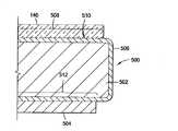
图2和2A示出了基板支架组件138另一实施方式的的部分截面图,为了避免混淆,该实施方式以下称为支架组件200。支架组件200包括主体202,其材质可为铝,并基本上涂覆有阳极电镀涂层210。主体202可由一个或多个耦合的元件或者具有加热元件132嵌入其中的整体成型的主体。基板支架组件实例可以采用2002年12月2日递交的美国专利申请10/308,385和2001年8月1日递交的美国专利申请09/921,104描述的发明权益,在此引用其两者的全部内容作为参考。FIGS. 2 and 2A show partial cross-sectional views of another embodiment of the
主体202通常包括基板支架表面204和相向的装配表面206。装配表面206与连接杆142相连(图1示)。阳极电镀涂层210至少涂覆主体202的基板支架表面204并在基板140和基板支架表面204之间提供分离层。The
参照图2A,涂层210包括外表面212和内表面214。内表面214通常直接设置于主体202上。在一实施方式中,阳极电镀涂层厚度约为0.3千分之一寸(7.6微米)到2.16千分之一寸(54.9微米)之间。厚度在此范围之外的电镀涂层在温度周期变化中常被损坏或者不能充分降低由PECVD形成的大面积氮化硅,α硅和n+α硅薄膜中的污点。Referring to FIG. 2A , coating 210 includes an outer surface 212 and an
参照图2和2A,位于基板支架表面204上的外表面212的一部分218具有设计用来支撑其上的基板140的几何形状。外表面212的一部分218有预定粗糙度的抛光面涂层216,其有助于在基板140上沉积厚度均匀的薄膜。抛光面涂层216的粗糙度约为200到2000微英寸。抛光面涂层216有利于提高薄膜厚度的均匀性以及尤其发现不需要调节(例如老化)支撑基板就可以基本上消除局部厚度的不一致(稀疏沉积的点)。免去支撑基板的调节节约了等离子体老化工艺所消耗的时间和材料以及免去了每个循环之间真空的清洗,免去的这些步骤致使系统的产量提高。在一实施方式中,抛光面涂层216的粗糙度约为330微英寸。Referring to Figures 2 and 2A, a
可以通过对基板140下面的基板支架外表面204的至少一部分220处理和/或通过至少对支撑基板140的阳极电镀涂层210进行处理(得到预定的抛光面208)来获得阳极电镀涂层210的抛光面涂层216。可以用多种方法形成基板支架表面204的抛光面208,包括珠光处理、喷磨、铣削、压印、砂纸打磨、蚀纹,刻蚀或其他方法获得预定的表面粗糙度。在一实施方式中,主体202的基板支架表面204的抛光面208约为200到2000微英寸。另一实施方式中,抛光面208约为330微英寸。The
或者,为了使制造成本最小,可以不对由220部分限定的基板支架表面204以外的窄带224进行处理。这将在未作处理的窄带224上产生阳极电镀涂层210的窄带222,与抛光面216相比,具有不同的抛光度,但是,由于窄带222在位于基板140以外,因此窄带222的抛光面对薄膜沉积的均匀性没有影响。在一实施方式中,阳极电镀涂层210的窄带222具有比阳极电镀涂层210限定的部分218具有更光滑的抛光面。Alternatively, to minimize manufacturing costs, the
图3描述了一制造支架组件138的方法300的实施方式。该方法开始的步骤302为制备主体202的基板支架表面204。制备步骤302通常需要加工或者对基板支架表面204进行其他处理从而得到约为200到2000微英寸之间的抛光面208。抛光面208用平均表面粗糙度(Ra)或者算术平均值(AA)来衡量。在一实施方式中,制备步骤302可以包括珠光处理、喷磨、铣削、压印、砂纸打磨、蚀纹,刻蚀或其他方法获得大约300微英寸的预定表面粗糙度。为了得到大于550到约2000微英寸左右的表面粗糙度,通常用研磨,车床切割,压花,火焰切割或其他类似的金属去除技术。FIG. 3 depicts an embodiment of a
在步骤302的实施方式中,通过诸如铝,三氧化二铝,钛或者不锈钢的材料对支撑基板表面204进行火焰、电弧或者等离子体喷涂以实现范围在约200到约2000微英寸之间的所需粗糙度。一方面,用电弧喷涂的铝材料涂覆基板支架表面204,得到200到2000微英寸左右的粗糙度。In an embodiment of
在一实施方式中,对基板支架表面204珠光处理至预定的抛光面。珠光处理过程可以包括用石榴石,陶瓷或者玻璃珠撞击主体202。In one embodiment, the
另一实施方式中,珠砂为氧化铝其平均直径为约125到约375微米。珠砂通过具有足够大的出射速度的管口提供该珠砂以得到大约200到2000微英寸左右的抛光面208。In another embodiment, the bead is alumina and has an average diameter of about 125 to about 375 microns. The bead is provided through an orifice having a sufficiently large exit velocity to obtain a
在制备步骤302完成后,在步骤304对主体进行阳极电镀。阳极电镀步骤304通常包括涂覆一层厚度约为0.3到2.16千分之一寸的阳极电镀层。阳极电镀涂层212的外表面210上最终得到的抛光面涂层216约为200到约2000微英寸,并且较理想地在约300到约1000微英寸之间,甚至更理想地在约330到500微英寸左右。After the
图4示出了制造支架组件138的方法400的另一实施方式。该方法开始步骤402为对主体202阳极电镀。在步骤404中,对阳极电镀涂层210的外表面212的至少一部分进行处理以提供粗糙的抛光面涂层216。或者,可对外表面212其他部分进行处理。FIG. 4 illustrates another embodiment of a
处理步骤404可包括珠光处理,喷磨,铣削,压印,砂纸打磨,蚀纹,刻蚀或其他方法获得指定的表面粗糙度。在一实施方式中,处理步骤404得到外表面的抛光面约在200到2000微英寸之间,和较理想地约在300到1000微英寸之间,以及更理想地约在330到500微英寸之间。Processing
图5示出了用于提高沉积厚度均匀性的支架组件500的另一实施方式的部分截面图。支架组件500包括基本上由阳极电镀涂层506覆盖的铝制支架主体502。加热元件504与该支架主体502相连以控制位于支架组件500上表面上的基板140的温度。加热元件504可为电阻加热器或者与主体502相连或者靠主体502设置的其他温度控制元件。或者,主体502的下部分512可以不用阳极电镀处理使加热元件504与主体502直接接触。任选地,导热材料的插入层(未示出)可设置在加热元件504和主体502的下部512之间。FIG. 5 shows a partial cross-sectional view of another embodiment of a
设置支撑基板140的阳极电镀涂层506的上部508具有抛光面510用来提高基板140上薄膜沉积的均匀性。在实施方式中,抛光面510的粗糙度约在200微英寸到约2000微英寸之间,并且较理想地约在300到约1000微英寸之间,以及更理想地约在330到500微英寸之间。可以通过多种方法包括以上所述的方法对抛光面510进行处理。The
图6示出了加热装置600的另一实施方式。加热装置600包括铝主体602其具有至少部分形成于其上的阳极电镀涂层606。也就是说,在主体602的底面上设置加热元件604以便于对基板140施加温度控制,该加热元件604为用于循环控制温度的循环液体的导管。或者,可以在加热元件604和主体602之间设置导热板614从而提高加热元件604和主体602之间的温度均匀性。在一实施方式中,导热板614为铜板。FIG. 6 shows another embodiment of a heating device 600 . The heating device 600 includes an aluminum body 602 having an anodized coating 606 at least partially formed thereon. That is, a heating element 604 is provided on the bottom surface of the main body 602 to apply temperature control to the
通过多个紧固件610(其中一个在图6示出)其装入主体602内形成的螺丝孔612中,模座板608与主体602相连。模座板608夹在加热元件604和主体之间,从而增强热传递。The base plate 608 is connected to the main body 602 by a plurality of fasteners 610 (one of which is shown in FIG. 6 ) which fit into screw holes 612 formed in the main body 602 . The die plate 608 is sandwiched between the heating element 604 and the body to enhance heat transfer.
设置支撑基板140的阳极电镀涂层606的一部分620具有抛光面622从而提高基板140上的薄膜沉积均匀性。抛光面622可以类似以上所述得到。A portion 620 of the anodized coating 606 on which the
因此,本发明提供了一种改进大面积基板上薄膜沉积均匀性的支架组件。蚀印涂覆有至少一部分阳极电镀涂层的支撑基板的支架组件的铝主体以得到预定的表面粗糙度来提高沉积均匀性,从而基本上免去了对支架组件耗费时间的老化和它的相关成本。Accordingly, the present invention provides a support assembly that improves the uniformity of thin film deposition on large area substrates. Etching the aluminum body of the support assembly of the support substrate coated with at least a portion of the anodized coating to obtain a predetermined surface roughness to enhance deposition uniformity, thereby substantially eliminating time-consuming aging of the support assembly and its associated cost.
无涂层基座uncoated base
图7和图7A示出了无涂层的支架组件138另一实施方式的部分截面图,为了避免混淆,以下将用基板支架组件700表示。该支架组件700包括裸露的,无涂层的主体702。主体702可以由一个或者多个耦合元件或者其中嵌有加热元件132的整体成型的主体组成。在一实施方式中,主体702由诸如铝、钛或者不锈钢的金属组成。7 and 7A illustrate partial cross-sectional views of another embodiment of an
主体702通常包括基板支架表面704和正对装配表面706。装配表面706与连接杆142连接(图1示出)。The body 702 generally includes a substrate support surface 704 and an opposing mounting surface 706 . The mounting surface 706 is connected to the connecting rod 142 (shown in FIG. 1 ).
参照图7和7A,设计基板支架表面704使其具有用于支撑其上的基板140的几何形状。基板支架表面704的基板接触部分具有预定粗糙度的抛光面714,其可以提高在基板140上沉积薄膜厚度的均匀性。抛光面714的粗糙度约为80到约2000微英寸之间。抛光面714有利于提高薄膜厚度的均匀性,以及发现尤其能基本上消除局部厚度不均匀性(稀疏沉积的点)。在一实施方式中,抛光面714具有大于约140微英寸的粗糙度。在另一实施方式中,抛光面714具有大于约340微英寸的粗糙度。一方面,有可能使基板接触部分720外的区域722,侧边734以及正对装配表面706处于非粗糙的或者部分粗糙的状态从而降低形成支撑基板装置700的成本是可行的。7 and 7A, the substrate support surface 704 is designed to have a geometry for supporting the
图8示出了制造基板支架组件138实施方式的方法。该方法开始于步骤802制备主体702的支架表面704。制备步骤802通常包括对基板支架704的加工或者处理得到抛光面714为约140到约2000微英寸之间,并且较理想地在约300到约1000微英寸之间,以及更理想地在约330到约500微英寸之间。抛光面714用平均表面粗糙度(Ra)或者算术平均值(AA)来表示。在一实施方式中,制备步骤802可以包括喷珠光处理、喷磨、铣削、压印、砂纸打磨、蚀纹,刻蚀或其他方法获大约330微英寸的预定表面粗糙度。为了得到大于500微英寸到约2000微英寸左右的表面粗糙度,通常用铣削、车床切割、压花、火焰切割或其他类似的金属去除方法。FIG. 8 illustrates a method of manufacturing an embodiment of a
在一实施方式中,采用任选的表面涂覆步骤804形成支撑基板的粗糙表面。可以采用常用的火焰,电弧或者等离子体喷涂诸如以铝,钛,或者不锈钢的金属在支撑表面704上执行表面涂覆步骤804,以得到范围约在140到约2000微英寸之间的所需的粗糙度。一方面,由铝组成的主体702的支架表面704用电弧喷涂的铝材料涂覆而得到大于约140微英寸的粗糙度。In one embodiment, an optional surface coating step 804 is used to roughen the surface of the support substrate. The surface coating step 804 may be performed on the support surface 704 using conventional flame, arc or plasma spraying metals such as aluminum, titanium, or stainless steel to obtain the desired thickness in the range of about 140 to about 2000 microinches. roughness. In one aspect, the stent surface 704 of the body 702 comprised of aluminum is coated with an arc sprayed aluminum material to a roughness greater than about 140 microinches.
在任选步骤804的另一实施方式中,利用常用的火焰、电弧或者等离子体喷涂工艺将陶瓷或者金属氧化物涂层沉积于支撑表面704上,而得到约在80到约2000微英寸之间的表面粗糙度。例如可将三氧化二铝沉积在基板支架704上得到约在140到约2000微英寸之间的粗糙度。In another embodiment of optional step 804, a ceramic or metal oxide coating is deposited on support surface 704 using conventional flame, arc, or plasma spray processes to obtain between about 80 and about 2000 microinches surface roughness. For example, Al2O3 may be deposited on the substrate support 704 to a roughness between about 140 and about 2000 microinches.
基板支架结构Substrate support structure
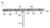
以上所述涉及本发明的各方面主要讨论了通过改进基板支架组件(例如,元件138,200,700)的各种性能和特点可改进大面积基板上的基板工艺效果的不同实施方式。为了在大面积基板上获得满意的和可重复的工艺效果,通常需要确保的一点是基板和基板支架之间的接触相对均匀并可重复。为了确保基板相对均匀和可重复,基板支架表面通常需要形成并保持一个所需和可重复的形状。参照图9和10,由于基板结构910的大小和工艺中常达到的温度因素(例如,通常为150℃到460℃),通常需要对基板支架902提供结构上的支撑(例如,元件910)以防它由于重力和形成基板支架902的材料的软化引起的偏移。由于铝材料在这些温度时的特性,在使用由铝组成的基板支架902时这个问题经常出现。用于防止在高温工艺过程中偏移的基板支架902内部的支撑结构的示例性设计在美国公开授予的6,554,907专利有更详细的描述,在此引用其全部内容作为参考。用于防止在高温工艺过程中偏移的基板支架902外部的支架结构其示例性设计在2005年6月2日递交的美国专利申请11/143,506[AMAT 9182]中有更详细的描述,该申请要求享有2004年7月12日递交的美国临时专利申请60/587,173的权益,在此引用其全部内容作为参考。The above-described aspects related to the present invention primarily discuss different embodiments in which the performance of substrate processing on large area substrates can be improved by improving various properties and characteristics of the substrate support assembly (eg,
图9示出了可用来取代图1所示的基板支架组件138的基板支架结构910其的等距分解图。图10示出了以在基板支架表面904上定位基板140的完全安装定位位置上的基板支架结构910的侧面图。图9和图10的基板支架结构910通常包括基板支架902下的基座结构914。一方面,基板支架902由基座结构914支撑,在连接点901处通过轴142连接和支撑该基座结构914。在一实施方式中,基座结构914用来给基座支架902提供连续的支撑来确保基板支架表面904在进行各种工艺之前,期间和之后保持所需的预定形状。可以由以上所述的任何一种工艺形成所述与支架结构910连接的基板支架902,(例如,所述的相关元件202,502,602,702)。FIG. 9 shows an isometric exploded view of a
基座结构914通常包含延长基座支撑板915和多个用于支撑基板支架902的侧面支撑板917。图9所示的结构中,通常以横穿基座支架板915的方向设置侧面支撑。一方面,板915,917最好用强度和硬度足够大的材料制造从而在工艺温度和压力条件下支撑和保持基板支架902的重量。例如,板915,917由陶瓷材料,例如氧化铝或者耐热金属诸如300系列不锈钢构成。The
为了说明起见,虽然图9只示出了基板支架结构的分解示意图,可以理解支架902直接安装在支架板915,917上。假设在工艺工程中,基板支架902和支架板915,917不会产生相对移动。此外,参照图9,虽然只示出了一个基座支架板915和四个独立的侧面支架板917,但是应当理解可以使用任意数目的支架板915,917。For the purpose of illustration, although FIG. 9 only shows an exploded view of the substrate support structure, it can be understood that the
在一实施方式中,基座结构914可形成为非平面形状从而可使非平面的结构与基板支架902和支撑的基板140相连(见图10)。在该实施方式中,基座结构914可以包含延长的基座支架板915,多个通常横向贯穿基座支架板915设置的侧面支架板917,以及安放于侧面支架板917上用来支撑基板支架902以及得到所需的非平面形状的多个不同厚度的垫片918。优选地,垫片918的厚度约为0.4mm到约3.5mm。该实施方式中,垫片918设置于侧边支架板917的末端,然而,垫片918可以放置于侧边支架板917的其他部分。可以考虑到支架板917的形状以及/或者垫片918的使用将允许基板支架预先成形,既在工艺工程中将所需的平面定向转移到基板上,由于在工艺过程中,加热的基板将遵循基板支架902的平面方向In one embodiment, the
尽管本发明结合多种优选实施方式进行详细说明和描述,本领域技术人员可以设计本发明的其他更多的实施方式。While the invention has been illustrated and described in conjunction with various preferred embodiments, those skilled in the art can devise other and more embodiments of the invention.
Claims (23)
Translated fromChineseApplications Claiming Priority (2)
| Application Number | Priority Date | Filing Date | Title |
|---|---|---|---|
| US11/182,168 | 2005-07-15 | ||
| US11/182,168US8372205B2 (en) | 2003-05-09 | 2005-07-15 | Reducing electrostatic charge by roughening the susceptor |
Publications (2)
| Publication Number | Publication Date |
|---|---|
| CN1897784A CN1897784A (en) | 2007-01-17 |
| CN1897784Btrue CN1897784B (en) | 2011-04-13 |
Family
ID=37610096
Family Applications (1)
| Application Number | Title | Priority Date | Filing Date |
|---|---|---|---|
| CN2006100985827AActiveCN1897784B (en) | 2005-07-15 | 2006-07-12 | Reducing electrostatic charge by roughening the susceptor |
Country Status (4)
| Country | Link |
|---|---|
| JP (1) | JP5361119B2 (en) |
| KR (1) | KR101441858B1 (en) |
| CN (1) | CN1897784B (en) |
| TW (1) | TWI375295B (en) |
Families Citing this family (13)
| Publication number | Priority date | Publication date | Assignee | Title |
|---|---|---|---|---|
| KR100927509B1 (en)* | 2007-05-23 | 2009-11-17 | 어플라이드 머티어리얼스, 인코포레이티드 | A method of depositing a silicon layer over a laser scribed transmissive conductive oxide layer suitable for use in the solar cell field |
| KR100938874B1 (en)* | 2007-07-24 | 2010-01-27 | 주식회사 에스에프에이 | Chemical vapor deposition apparatus comprising a susceptor for supporting a glass substrate, a method of manufacturing the same, and a susceptor for supporting the glass substrate |
| CN102233580A (en)* | 2010-05-06 | 2011-11-09 | 日月光半导体制造股份有限公司 | Suction nozzle and automatic handling device |
| CN102842636B (en)* | 2011-06-20 | 2015-09-30 | 理想能源设备(上海)有限公司 | For the base plate heating pedestal of chemical gas-phase deposition system |
| TWI477630B (en)* | 2011-10-18 | 2015-03-21 | Au Optronics Corp | Thin film deposition apparatus and bearing element thereof |
| CN111485226A (en)* | 2012-07-27 | 2020-08-04 | 应用材料公司 | Roughened substrate support |
| CN103151235B (en)* | 2013-02-20 | 2016-01-27 | 上海华力微电子有限公司 | A kind of device improving etching homogeneity |
| CN105407620A (en)* | 2015-12-14 | 2016-03-16 | 重庆瑞阳科技股份有限公司 | Static conductive apparatus |
| CN107393803A (en)* | 2017-07-28 | 2017-11-24 | 武汉华星光电技术有限公司 | Lower electrode arrangement and dry ecthing board for dry ecthing board |
| KR102080231B1 (en) | 2018-03-30 | 2020-02-21 | (주)티티에스 | Susceptor |
| KR20210128063A (en)* | 2020-04-16 | 2021-10-26 | 주식회사 제우스 | Energizing device for substrate |
| KR102811162B1 (en)* | 2020-04-16 | 2025-05-26 | 주식회사 제우스 | Energizing device for substrate processing |
| KR20230104183A (en)* | 2020-11-06 | 2023-07-07 | 코닝 인코포레이티드 | Substrates with improved electrostatic performance |
Citations (6)
| Publication number | Priority date | Publication date | Assignee | Title |
|---|---|---|---|---|
| US5200157A (en)* | 1986-02-17 | 1993-04-06 | Toshiba Ceramics Co., Ltd. | Susceptor for vapor-growth deposition |
| US5384682A (en)* | 1993-03-22 | 1995-01-24 | Toto Ltd. | Electrostatic chuck |
| US5844205A (en)* | 1996-04-19 | 1998-12-01 | Applied Komatsu Technology, Inc. | Heated substrate support structure |
| US6063203A (en)* | 1997-06-06 | 2000-05-16 | Asm Japan K.K. | Susceptor for plasma CVD equipment and process for producing the same |
| CN1491435A (en)* | 2001-02-16 | 2004-04-21 | ������������ʽ���� | Method and apparatus for transferring heat from substrate to chuck |
| CN1551326A (en)* | 2003-05-09 | 2004-12-01 | Ӧ�ò��Ϲ�˾ | Anodized Substrate Supports |
Family Cites Families (2)
| Publication number | Priority date | Publication date | Assignee | Title |
|---|---|---|---|---|
| JP3788836B2 (en)* | 1996-12-24 | 2006-06-21 | 東芝セラミックス株式会社 | Vapor growth susceptor and manufacturing method thereof |
| JP3758979B2 (en)* | 2001-02-27 | 2006-03-22 | 京セラ株式会社 | Electrostatic chuck and processing apparatus |
- 2006
- 2006-06-22TWTW095122556Apatent/TWI375295B/enactive
- 2006-07-12CNCN2006100985827Apatent/CN1897784B/enactiveActive
- 2006-07-13KRKR1020060065971Apatent/KR101441858B1/enactiveActive
- 2006-07-14JPJP2006194506Apatent/JP5361119B2/enactiveActive
Patent Citations (6)
| Publication number | Priority date | Publication date | Assignee | Title |
|---|---|---|---|---|
| US5200157A (en)* | 1986-02-17 | 1993-04-06 | Toshiba Ceramics Co., Ltd. | Susceptor for vapor-growth deposition |
| US5384682A (en)* | 1993-03-22 | 1995-01-24 | Toto Ltd. | Electrostatic chuck |
| US5844205A (en)* | 1996-04-19 | 1998-12-01 | Applied Komatsu Technology, Inc. | Heated substrate support structure |
| US6063203A (en)* | 1997-06-06 | 2000-05-16 | Asm Japan K.K. | Susceptor for plasma CVD equipment and process for producing the same |
| CN1491435A (en)* | 2001-02-16 | 2004-04-21 | ������������ʽ���� | Method and apparatus for transferring heat from substrate to chuck |
| CN1551326A (en)* | 2003-05-09 | 2004-12-01 | Ӧ�ò��Ϲ�˾ | Anodized Substrate Supports |
Also Published As
| Publication number | Publication date |
|---|---|
| TW200707627A (en) | 2007-02-16 |
| KR101441858B1 (en) | 2014-09-19 |
| TWI375295B (en) | 2012-10-21 |
| KR20070009450A (en) | 2007-01-18 |
| JP2007051367A (en) | 2007-03-01 |
| JP5361119B2 (en) | 2013-12-04 |
| CN1897784A (en) | 2007-01-17 |
Similar Documents
| Publication | Publication Date | Title |
|---|---|---|
| CN1897784B (en) | Reducing electrostatic charge by roughening the susceptor | |
| US8372205B2 (en) | Reducing electrostatic charge by roughening the susceptor | |
| CN100385640C (en) | Anodized Substrate Supports | |
| JP5578762B2 (en) | Plasma reactor substrate incorporating surface texturing | |
| US20050120962A1 (en) | Substrate supporting table, method for producing same, and processing system | |
| JP2005051200A5 (en) | ||
| TW200901363A (en) | Substrate carrying bench and substrate treatment device | |
| US20120037314A1 (en) | Substrate processing apparatus and side wall component | |
| JP2006351949A (en) | Substrate mounting table, substrate processing apparatus, and method for manufacturing substrate mounting table | |
| CN104241183A (en) | Manufacturing method of electrostatic suction cup, electrostatic suction cup and plasma processing device | |
| JP4709047B2 (en) | Substrate processing apparatus and side wall parts | |
| CN104241182B (en) | The manufacture method of electrostatic chuck, electrostatic chuck and plasma processing apparatus | |
| CN101978473B (en) | Base with roll-formed surface and method of manufacturing same | |
| KR20200094781A (en) | Partially anodized shower head | |
| CN104241181A (en) | Method for manufacturing electrostatic chuck, electrostatic chuck and plasma processing device thereof | |
| CN115213808B (en) | Polishing method of substrate mounting table and substrate processing device |
Legal Events
| Date | Code | Title | Description |
|---|---|---|---|
| C06 | Publication | ||
| PB01 | Publication | ||
| C10 | Entry into substantive examination | ||
| SE01 | Entry into force of request for substantive examination | ||
| C14 | Grant of patent or utility model | ||
| GR01 | Patent grant | ||
| C56 | Change in the name or address of the patentee | ||
| CP01 | Change in the name or title of a patent holder | Address after:American California Patentee after:Applied Materials Inc. Address before:American California Patentee before:Applied Materials Inc. |