CN1897270B - Wiring structure, method of manufacturing wiring, thin film transistor substrate and method of manufacturing the same - Google Patents
Wiring structure, method of manufacturing wiring, thin film transistor substrate and method of manufacturing the sameDownload PDFInfo
- Publication number
- CN1897270B CN1897270BCN200610099012XACN200610099012ACN1897270BCN 1897270 BCN1897270 BCN 1897270BCN 200610099012X ACN200610099012X ACN 200610099012XACN 200610099012 ACN200610099012 ACN 200610099012ACN 1897270 BCN1897270 BCN 1897270B
- Authority
- CN
- China
- Prior art keywords
- layer
- copper
- barrier layer
- substrate
- gate
- Prior art date
- Legal status (The legal status is an assumption and is not a legal conclusion. Google has not performed a legal analysis and makes no representation as to the accuracy of the status listed.)
- Expired - Fee Related
Links
Images


Classifications
- G—PHYSICS
- G02—OPTICS
- G02F—OPTICAL DEVICES OR ARRANGEMENTS FOR THE CONTROL OF LIGHT BY MODIFICATION OF THE OPTICAL PROPERTIES OF THE MEDIA OF THE ELEMENTS INVOLVED THEREIN; NON-LINEAR OPTICS; FREQUENCY-CHANGING OF LIGHT; OPTICAL LOGIC ELEMENTS; OPTICAL ANALOGUE/DIGITAL CONVERTERS
- G02F1/00—Devices or arrangements for the control of the intensity, colour, phase, polarisation or direction of light arriving from an independent light source, e.g. switching, gating or modulating; Non-linear optics
- G02F1/01—Devices or arrangements for the control of the intensity, colour, phase, polarisation or direction of light arriving from an independent light source, e.g. switching, gating or modulating; Non-linear optics for the control of the intensity, phase, polarisation or colour
- G02F1/13—Devices or arrangements for the control of the intensity, colour, phase, polarisation or direction of light arriving from an independent light source, e.g. switching, gating or modulating; Non-linear optics for the control of the intensity, phase, polarisation or colour based on liquid crystals, e.g. single liquid crystal display cells
- G02F1/133—Constructional arrangements; Operation of liquid crystal cells; Circuit arrangements
- G02F1/136—Liquid crystal cells structurally associated with a semi-conducting layer or substrate, e.g. cells forming part of an integrated circuit
- H—ELECTRICITY
- H01—ELECTRIC ELEMENTS
- H01L—SEMICONDUCTOR DEVICES NOT COVERED BY CLASS H10
- H01L23/00—Details of semiconductor or other solid state devices
- H01L23/52—Arrangements for conducting electric current within the device in operation from one component to another, i.e. interconnections, e.g. wires, lead frames
- H01L23/522—Arrangements for conducting electric current within the device in operation from one component to another, i.e. interconnections, e.g. wires, lead frames including external interconnections consisting of a multilayer structure of conductive and insulating layers inseparably formed on the semiconductor body
- H01L23/532—Arrangements for conducting electric current within the device in operation from one component to another, i.e. interconnections, e.g. wires, lead frames including external interconnections consisting of a multilayer structure of conductive and insulating layers inseparably formed on the semiconductor body characterised by the materials
- H01L23/53204—Conductive materials
- H01L23/53209—Conductive materials based on metals, e.g. alloys, metal silicides
- H01L23/53228—Conductive materials based on metals, e.g. alloys, metal silicides the principal metal being copper
- H01L23/53238—Additional layers associated with copper layers, e.g. adhesion, barrier, cladding layers
- H—ELECTRICITY
- H10—SEMICONDUCTOR DEVICES; ELECTRIC SOLID-STATE DEVICES NOT OTHERWISE PROVIDED FOR
- H10D—INORGANIC ELECTRIC SEMICONDUCTOR DEVICES
- H10D30/00—Field-effect transistors [FET]
- H10D30/60—Insulated-gate field-effect transistors [IGFET]
- H10D30/67—Thin-film transistors [TFT]
- H10D30/6729—Thin-film transistors [TFT] characterised by the electrodes
- H10D30/6737—Thin-film transistors [TFT] characterised by the electrodes characterised by the electrode materials
- H10D30/6739—Conductor-insulator-semiconductor electrodes
- H—ELECTRICITY
- H10—SEMICONDUCTOR DEVICES; ELECTRIC SOLID-STATE DEVICES NOT OTHERWISE PROVIDED FOR
- H10D—INORGANIC ELECTRIC SEMICONDUCTOR DEVICES
- H10D30/00—Field-effect transistors [FET]
- H10D30/60—Insulated-gate field-effect transistors [IGFET]
- H10D30/67—Thin-film transistors [TFT]
- H10D30/674—Thin-film transistors [TFT] characterised by the active materials
- H10D30/6741—Group IV materials, e.g. germanium or silicon carbide
- H10D30/6743—Silicon
- H—ELECTRICITY
- H10—SEMICONDUCTOR DEVICES; ELECTRIC SOLID-STATE DEVICES NOT OTHERWISE PROVIDED FOR
- H10D—INORGANIC ELECTRIC SEMICONDUCTOR DEVICES
- H10D86/00—Integrated devices formed in or on insulating or conducting substrates, e.g. formed in silicon-on-insulator [SOI] substrates or on stainless steel or glass substrates
- H10D86/40—Integrated devices formed in or on insulating or conducting substrates, e.g. formed in silicon-on-insulator [SOI] substrates or on stainless steel or glass substrates characterised by multiple TFTs
- H10D86/441—Interconnections, e.g. scanning lines
- H—ELECTRICITY
- H10—SEMICONDUCTOR DEVICES; ELECTRIC SOLID-STATE DEVICES NOT OTHERWISE PROVIDED FOR
- H10D—INORGANIC ELECTRIC SEMICONDUCTOR DEVICES
- H10D86/00—Integrated devices formed in or on insulating or conducting substrates, e.g. formed in silicon-on-insulator [SOI] substrates or on stainless steel or glass substrates
- H10D86/40—Integrated devices formed in or on insulating or conducting substrates, e.g. formed in silicon-on-insulator [SOI] substrates or on stainless steel or glass substrates characterised by multiple TFTs
- H10D86/60—Integrated devices formed in or on insulating or conducting substrates, e.g. formed in silicon-on-insulator [SOI] substrates or on stainless steel or glass substrates characterised by multiple TFTs wherein the TFTs are in active matrices
- G—PHYSICS
- G02—OPTICS
- G02F—OPTICAL DEVICES OR ARRANGEMENTS FOR THE CONTROL OF LIGHT BY MODIFICATION OF THE OPTICAL PROPERTIES OF THE MEDIA OF THE ELEMENTS INVOLVED THEREIN; NON-LINEAR OPTICS; FREQUENCY-CHANGING OF LIGHT; OPTICAL LOGIC ELEMENTS; OPTICAL ANALOGUE/DIGITAL CONVERTERS
- G02F1/00—Devices or arrangements for the control of the intensity, colour, phase, polarisation or direction of light arriving from an independent light source, e.g. switching, gating or modulating; Non-linear optics
- G02F1/01—Devices or arrangements for the control of the intensity, colour, phase, polarisation or direction of light arriving from an independent light source, e.g. switching, gating or modulating; Non-linear optics for the control of the intensity, phase, polarisation or colour
- G02F1/13—Devices or arrangements for the control of the intensity, colour, phase, polarisation or direction of light arriving from an independent light source, e.g. switching, gating or modulating; Non-linear optics for the control of the intensity, phase, polarisation or colour based on liquid crystals, e.g. single liquid crystal display cells
- G02F1/133—Constructional arrangements; Operation of liquid crystal cells; Circuit arrangements
- G02F1/136—Liquid crystal cells structurally associated with a semi-conducting layer or substrate, e.g. cells forming part of an integrated circuit
- G02F1/1362—Active matrix addressed cells
- G02F1/136286—Wiring, e.g. gate line, drain line
- G02F1/13629—Multilayer wirings
- G—PHYSICS
- G02—OPTICS
- G02F—OPTICAL DEVICES OR ARRANGEMENTS FOR THE CONTROL OF LIGHT BY MODIFICATION OF THE OPTICAL PROPERTIES OF THE MEDIA OF THE ELEMENTS INVOLVED THEREIN; NON-LINEAR OPTICS; FREQUENCY-CHANGING OF LIGHT; OPTICAL LOGIC ELEMENTS; OPTICAL ANALOGUE/DIGITAL CONVERTERS
- G02F1/00—Devices or arrangements for the control of the intensity, colour, phase, polarisation or direction of light arriving from an independent light source, e.g. switching, gating or modulating; Non-linear optics
- G02F1/01—Devices or arrangements for the control of the intensity, colour, phase, polarisation or direction of light arriving from an independent light source, e.g. switching, gating or modulating; Non-linear optics for the control of the intensity, phase, polarisation or colour
- G02F1/13—Devices or arrangements for the control of the intensity, colour, phase, polarisation or direction of light arriving from an independent light source, e.g. switching, gating or modulating; Non-linear optics for the control of the intensity, phase, polarisation or colour based on liquid crystals, e.g. single liquid crystal display cells
- G02F1/133—Constructional arrangements; Operation of liquid crystal cells; Circuit arrangements
- G02F1/136—Liquid crystal cells structurally associated with a semi-conducting layer or substrate, e.g. cells forming part of an integrated circuit
- G02F1/1362—Active matrix addressed cells
- G02F1/136286—Wiring, e.g. gate line, drain line
- G02F1/136295—Materials; Compositions; Manufacture processes
- H—ELECTRICITY
- H01—ELECTRIC ELEMENTS
- H01L—SEMICONDUCTOR DEVICES NOT COVERED BY CLASS H10
- H01L2924/00—Indexing scheme for arrangements or methods for connecting or disconnecting semiconductor or solid-state bodies as covered by H01L24/00
- H01L2924/0001—Technical content checked by a classifier
- H01L2924/0002—Not covered by any one of groups H01L24/00, H01L24/00 and H01L2224/00
- H—ELECTRICITY
- H01—ELECTRIC ELEMENTS
- H01L—SEMICONDUCTOR DEVICES NOT COVERED BY CLASS H10
- H01L2924/00—Indexing scheme for arrangements or methods for connecting or disconnecting semiconductor or solid-state bodies as covered by H01L24/00
- H01L2924/10—Details of semiconductor or other solid state devices to be connected
- H01L2924/11—Device type
- H01L2924/12—Passive devices, e.g. 2 terminal devices
- H01L2924/1204—Optical Diode
- H01L2924/12044—OLED
- H—ELECTRICITY
- H01—ELECTRIC ELEMENTS
- H01L—SEMICONDUCTOR DEVICES NOT COVERED BY CLASS H10
- H01L2924/00—Indexing scheme for arrangements or methods for connecting or disconnecting semiconductor or solid-state bodies as covered by H01L24/00
- H01L2924/30—Technical effects
- H01L2924/301—Electrical effects
- H01L2924/3011—Impedance
- H—ELECTRICITY
- H10—SEMICONDUCTOR DEVICES; ELECTRIC SOLID-STATE DEVICES NOT OTHERWISE PROVIDED FOR
- H10D—INORGANIC ELECTRIC SEMICONDUCTOR DEVICES
- H10D30/00—Field-effect transistors [FET]
- H10D30/60—Insulated-gate field-effect transistors [IGFET]
- H10D30/67—Thin-film transistors [TFT]
- H10D30/6729—Thin-film transistors [TFT] characterised by the electrodes
- Y—GENERAL TAGGING OF NEW TECHNOLOGICAL DEVELOPMENTS; GENERAL TAGGING OF CROSS-SECTIONAL TECHNOLOGIES SPANNING OVER SEVERAL SECTIONS OF THE IPC; TECHNICAL SUBJECTS COVERED BY FORMER USPC CROSS-REFERENCE ART COLLECTIONS [XRACs] AND DIGESTS
- Y10—TECHNICAL SUBJECTS COVERED BY FORMER USPC
- Y10T—TECHNICAL SUBJECTS COVERED BY FORMER US CLASSIFICATION
- Y10T29/00—Metal working
- Y10T29/49—Method of mechanical manufacture
- Y10T29/49002—Electrical device making
- Y10T29/49117—Conductor or circuit manufacturing
Landscapes
- Physics & Mathematics (AREA)
- General Physics & Mathematics (AREA)
- Microelectronics & Electronic Packaging (AREA)
- Engineering & Computer Science (AREA)
- Condensed Matter Physics & Semiconductors (AREA)
- Nonlinear Science (AREA)
- Computer Hardware Design (AREA)
- Power Engineering (AREA)
- Crystallography & Structural Chemistry (AREA)
- Chemical & Material Sciences (AREA)
- Optics & Photonics (AREA)
- Mathematical Physics (AREA)
- Thin Film Transistor (AREA)
- Internal Circuitry In Semiconductor Integrated Circuit Devices (AREA)
- Electrodes Of Semiconductors (AREA)
Abstract
Description
Translated fromChinese相关申请的交叉参考Cross References to Related Applications
本申请要求于2005年7月15日在韩国知识产权局提交的韩国专利申请第10-2005-0064483号中的优先权,其全部内容结合于此作为参考。This application claims priority from Korean Patent Application No. 10-2005-0064483 filed in the Korean Intellectual Property Office on Jul. 15, 2005, the entire contents of which are hereby incorporated by reference.
技术领域technical field
本发明涉及布线结构,并且更特别地,涉及一种包括铜(Cu)或铜合金的布线结构、一种用于制造布线的方法、一种薄膜晶体管(TFT)基板、以及一种用于制造TFT基板的方法。The present invention relates to wiring structures, and more particularly, to a wiring structure including copper (Cu) or a copper alloy, a method for manufacturing wiring, a thin film transistor (TFT) substrate, and a method for manufacturing method of TFT substrate.
背景技术Background technique
薄膜晶体管(TFT)基板被用作用于具有矩阵阵列中的像素的液晶显示器(LCD)和有机电致发光(EL)显示器的基板。Thin film transistor (TFT) substrates are used as substrates for liquid crystal displays (LCD) and organic electroluminescent (EL) displays having pixels in a matrix array.
LCD作为最广泛使用的平板显示器之一,包括两个具有多个电极的基板以及置于其间的液晶层,并且通过向电极施加电压以重新排列液晶层中的液晶分子来调节穿过其传输的光量。在LCD中,薄膜晶体管被用作用于控制施加到各个电极的图像信号的开关元件。LCD, one of the most widely used flat-panel displays, consists of two substrates with multiple electrodes and a liquid crystal layer interposed between them, and the liquid crystal molecules transmitted through them are adjusted by applying voltage to the electrodes to rearrange the liquid crystal molecules in the liquid crystal layer. amount of light. In LCDs, thin film transistors are used as switching elements for controlling image signals applied to respective electrodes.
有机电致发光(EL)显示装置通过电激励磷光有机材料来显示图像,并且包括用于向像素提供发光所需的电流的驱动TFT和开关TFT。An organic electroluminescent (EL) display device displays images by electro-exciting phosphorescent organic materials, and includes driving TFTs and switching TFTs for supplying current required for light emission to pixels.
随着LCD或有机EL显示装置的显示面积的增加,连接至TFT的栅极线和数据线也变长,导致布线阻抗的增加。为了解决由阻抗增加而导致的信号延迟问题,栅极线和数据线应当由具有尽可能低的电阻率的材料来形成。As the display area of an LCD or organic EL display device increases, gate lines and data lines connected to TFTs also become longer, resulting in an increase in wiring resistance. In order to solve the signal delay problem caused by the increase in impedance, the gate line and the data line should be formed of a material having as low a resistivity as possible.
另外,为了改善布线的可靠性,要求布线具有良好的粘附性并图案化为具有良好剖面。In addition, in order to improve the reliability of the wiring, it is required that the wiring has good adhesion and is patterned to have a good profile.
发明内容Contents of the invention
本发明提供了一种具有铜布线结构的薄膜晶体管(TFT)基板,其中,铜布线结构展示出改进的粘附性和出色的侧剖面。本发明还提供了一种用于制造该TFT基板的方法。The present invention provides a thin film transistor (TFT) substrate having a copper wiring structure, wherein the copper wiring structure exhibits improved adhesion and excellent side profile. The present invention also provides a method for manufacturing the TFT substrate.
根据本发明的一个方面,提供了一种布线结构,其包括阻隔层(barrier layer),形成在基板上,优选地包括氮化铜,以及铜导电层,形成在阻隔层上并且包括铜或铜合金。According to one aspect of the present invention, there is provided a wiring structure comprising a barrier layer formed on a substrate, preferably comprising copper nitride, and a copper conductive layer formed on the barrier layer and comprising copper or copper alloy.
根据本发明的另一方面,提供了一种用于制造布线的方法,该方法包括:在基板上形成包括氮化铜的阻隔层;在阻隔层上形成包括铜或铜合金的铜导电层;在铜导电层上形成包括钼或钼合金的保护层(capping layer);以及使用限定布线的光刻胶图样作为蚀刻掩模来使保护层、铜导电层、以及阻隔层图样化。According to another aspect of the present invention, there is provided a method for manufacturing wiring, the method comprising: forming a barrier layer including copper nitride on a substrate; forming a copper conductive layer including copper or a copper alloy on the barrier layer; forming a capping layer including molybdenum or a molybdenum alloy on the copper conductive layer; and patterning the capping layer, the copper conductive layer, and the barrier layer using the photoresist pattern defining the wiring as an etch mask.
根据本发明的又一方面,提供了一种TFT基板,包括:在第一方向延伸的栅极布线和栅极线;在绝缘基板上连接至栅极线的栅电极;与栅极布线绝缘的数据布线;在第二方向延伸并与栅极线交叉的数据线;连接至数据线的源电极;在绝缘基板上与源电极隔开的漏电极;以及在栅极布线和数据布线上为每个像素形成的并连接至漏电极的像素电极,其中,栅极布线和/或数据布线包括形成在基板上并且包括氮化铜的阻隔层以及形成在阻隔层上并且包括铜或铜合金的铜导电层。According to still another aspect of the present invention, there is provided a TFT substrate, comprising: a gate wiring and a gate line extending in a first direction; a gate electrode connected to the gate line on an insulating substrate; data wiring; a data line extending in the second direction and crossing the gate line; a source electrode connected to the data line; a drain electrode separated from the source electrode on the insulating substrate; A pixel electrode formed for each pixel and connected to a drain electrode, wherein the gate wiring and/or the data wiring includes a barrier layer formed on the substrate and including copper nitride and copper formed on the barrier layer and including copper or a copper alloy conductive layer.
根据本发明的又一方面,提供了一种用于制造薄膜晶体管(TFT)基板的方法,该方法包括:在绝缘基板上形成包括在第一方向延伸的栅极线和连接至栅极线的栅电极的栅极布线;在绝缘基板上形成与栅极布线绝缘的数据布线,数据布线包括在第二方向延伸并与栅极线交叉的数据线、连接至数据线的源电极、以及与源电极隔开的漏电极;以及在栅极布线和数据布线上形成连接至每个像素的漏电极的像素电极,其中,形成栅极布线和/或数据布线包括:在基板上形成包括氮化铜的阻隔层;在阻隔层上形成包括铜或铜合金的铜导电层;在铜导电层上形成包括钼或钼合金的保护层;以及使用限定布线的光刻胶图样作为蚀刻掩模来使保护层、铜导电层、以及阻隔层图样化。According to still another aspect of the present invention, there is provided a method for manufacturing a thin film transistor (TFT) substrate, the method comprising: forming on an insulating substrate including a gate line extending in a first direction and a gate line connected to the gate line; Gate wiring of the gate electrode; data wiring insulated from the gate wiring is formed on the insulating substrate, the data wiring includes a data line extending in the second direction and crossing the gate line, a source electrode connected to the data line, and a source electrode connected to the source a drain electrode separated by electrodes; and forming a pixel electrode connected to the drain electrode of each pixel on the gate wiring and the data wiring, wherein forming the gate wiring and/or the data wiring includes: forming a copper nitride layer on the substrate a barrier layer; forming a copper conductive layer comprising copper or copper alloy on the barrier layer; forming a protective layer comprising molybdenum or molybdenum alloy on the copper conductive layer; layer, copper conductive layer, and barrier layer are patterned.
附图说明Description of drawings
通过参照附图来详细描述本发明的优选实施例,本发明的上述和其他特征和优点将变得更加显而易见,在附图中:The above and other features and advantages of the present invention will become more apparent by describing in detail preferred embodiments of the present invention with reference to the accompanying drawings, in which:
图1是示出了根据本发明的实施例的布线结构的截面图;FIG. 1 is a cross-sectional view showing a wiring structure according to an embodiment of the present invention;
图2示出了形成在基板上的根据本发明的实施例的布线结构的面间接触(interfacial contact);2 shows an interfacial contact (interfacial contact) of a wiring structure formed on a substrate according to an embodiment of the present invention;
图3和图4是示出了根据本发明的实施例的制造布线的方法的处理步骤的截面图;3 and 4 are cross-sectional views illustrating processing steps of a method of manufacturing wiring according to an embodiment of the present invention;
图5A是示出了通过根据本发明的实施例的布线制造方法制成的布线结构的显微照片;5A is a micrograph showing a wiring structure made by a wiring manufacturing method according to an embodiment of the present invention;
图5B是示出了通过根据本发明的实施例的布线制造方法制成的布线结构的截面图;5B is a cross-sectional view showing a wiring structure made by a wiring manufacturing method according to an embodiment of the present invention;
图6A是示出了根据本发明的实施例的薄膜晶体管(TFT)基板的布局图;6A is a layout diagram illustrating a thin film transistor (TFT) substrate according to an embodiment of the present invention;
图6B是沿着图6A中的线B-B’截取的截面图;Figure 6B is a cross-sectional view taken along line B-B' in Figure 6A;
图7A、8A、9A、和10A是顺序地示出根据本发明的实施例的用于制造TFT基板的方法的布局图;7A, 8A, 9A, and 10A are layout views sequentially illustrating a method for manufacturing a TFT substrate according to an embodiment of the present invention;
图7B、8B、9B、和10B是沿着图7A、8A、9A、和10A中的线B-B’截取的截面图;7B, 8B, 9B, and 10B are cross-sectional views along the line B-B' in FIGS. 7A, 8A, 9A, and 10A;
图11A是示出了根据本发明的实施例的TFT基板的另一实例的布局图;11A is a layout diagram showing another example of a TFT substrate according to an embodiment of the present invention;
图11B是沿着图11A中的线B-B’截取的截面图;Fig. 11B is a cross-sectional view taken along line B-B' in Fig. 11A;
图12A是示出了根据本发明的另一实施例的TFT基板的布局图;12A is a layout diagram showing a TFT substrate according to another embodiment of the present invention;
图12B和12C是沿着图12A中的线B-B’和C-C’截取的截面图;12B and 12C are cross-sectional views taken along lines B-B' and C-C' in FIG. 12A;
图13A、14A、15A、16A、17A、和18A是顺序地示出根据本发明的另一实施例的用于制造TFT基板的方法的布局图;13A, 14A, 15A, 16A, 17A, and 18A are layout views sequentially illustrating a method for manufacturing a TFT substrate according to another embodiment of the present invention;
图13B、14B、15B、16B、17B、和18B是沿着图13A、14A、15A、16A、17A、和18A中的线B-B’截取的示出了处理步骤的截面图;以及13B, 14B, 15B, 16B, 17B, and 18B are cross-sectional views showing processing steps taken along line B-B' in FIGS. 13A, 14A, 15A, 16A, 17A, and 18A; and
图13C、14C、15C、16C、17C、和18C是沿着图13A、14A、15A、16A、17A、和18A中的线C-C’截取的示出了处理步骤的截面图。13C, 14C, 15C, 16C, 17C, and 18C are cross-sectional views showing processing steps taken along line C-C' in FIGS. 13A, 14A, 15A, 16A, 17A, and 18A.
具体实施方式Detailed ways
以下将参照附图来全面地描述本发明,其中,附图示出了本发明的优选实施例。然而,本发明也可以通过多种不同的形式来实现,而不应理解为局限于在此所列举的实施例。相反,提供这些实施例,以便使公开透彻和完整,并且向本领域的技术人员充分地传达本发明的思想。在整篇说明书始终,相同的参考标号指示相同的元件。在附图中,为了清楚起见,放大了层和区域的厚度。The present invention will now be fully described with reference to the accompanying drawings, in which preferred embodiments of the invention are shown. However, this invention may be embodied in many different forms and should not be construed as limited to the embodiments set forth herein. Rather, these embodiments are provided so that this disclosure will be thorough and complete, and will fully convey the concept of the invention to those skilled in the art. Throughout the specification, the same reference numerals refer to the same elements. In the drawings, the thickness of layers and regions are exaggerated for clarity.
应当理解,当提到层“位于”另一层或基板上时,其可以直接在另一层或基板上,或者还可以存在插入层。相反,当提到元件“直接位于”另一元件上时,不存在插入元件。It will be understood that when a layer is referred to as being "on" another layer or substrate, it can be directly on the other layer or substrate, or intervening layers may also be present. In contrast, when an element is referred to as being "directly on" another element, there are no intervening elements present.
为了便于说明,在此可能使用诸如“在...之下”、“在...下面”、“下面的”、“在...上面”、以及“上面的”等的空间关系术语,以描述如图中所示的一个元件或机构与另一元件或机构的关系。应当理解,除了图中所示的方位之外,空间关系术语还将包括使用或操作中的装置的各种不同方位。例如,如果翻转图中所示的装置,则被描述为在其他元件或机构“下面”或“之下”的元件将被定位为在其他元件或机构的“上面”。因此,示例性术语“在...下面”包括在上面和在下面的方位。装置可以以其它方式定位(旋转90度或在其他方位),并且通过在此使用的空间关系描述符进行相应地解释。For ease of description, spatial relational terms such as "under", "beneath", "beneath", "above", and "above" may be used herein, To describe the relationship of one element or mechanism to another element or mechanism as shown in the figures. It will be understood that the spatially relative terms will encompass various orientations of the device in use or operation in addition to the orientation depicted in the figures. For example, if the device in the figures is turned over, elements described as "below" or "beneath" other elements or features would then be oriented "above" the other elements or features. Thus, the exemplary term "below" encompasses an orientation of above as well as below. A device may be otherwise oriented (rotated 90 degrees or at other orientations) and interpreted accordingly by the spatially relative descriptors used herein.
除非文中另有指出或明显违背上下文,在描述本发明的上下文中(特别是在随后的权利要求中)使用的术语“一个”、“这个”以及类似指示词包括单数和复数。除非另有注释,术语“包含”、“具有”、“包括”和“含有”可以解释为可扩展术语。As used in the context of describing the invention, and particularly in the following claims, the terms "a," "the," and similar designators include both the singular and the plural unless otherwise indicated by context or otherwise clearly contradicted by context. Unless otherwise noted, the terms "comprising", "having", "including" and "containing" are to be construed as expansive terms.
除非另有限定,在此所采用的所有技术术语和科技术语具有与本发明所属领域的普通技术人员通常所理解的相同解释。应当注意,除非另外指出,对于在此提供的任何和全部实例或示例性术语的使用,目的仅在于更好地说明本发明而不是限制本发明的范围。此外,除非另有限定,不能过度解释在通用字典中定义的所有术语。Unless otherwise defined, all technical and scientific terms used herein have the same meaning as commonly understood by one of ordinary skill in the art to which this invention belongs. It should be noted that the use of any and all examples, or exemplary terms, provided herein is intended merely to better illuminate the invention and is not intended to limit the scope of the invention unless otherwise indicated. Furthermore, all terms defined in general dictionaries should not be over-interpreted unless otherwise defined.
将参照透视图、横截面图、和/或平面图来描述本发明,其中示出了本发明的优选实施例。因此,可以根据制造技术和/或定量配额来修改示例性视图的轮廓。即,本发明的实施例并非用于限制本发明的范围,而是覆盖可以由于制造工艺的变化而引起的所有变化和修改。因此,附图中示出的区域是以示意性形式来说明,并且区域的形状仅通过说明的方式来表示而不是作为限制。The invention will be described with reference to perspective views, cross-sections, and/or plan views, in which preferred embodiments of the invention are shown. Accordingly, the outlines of the exemplary views may be modified according to manufacturing techniques and/or quantitative quotas. That is, the embodiments of the present invention are not intended to limit the scope of the present invention, but cover all changes and modifications that may be caused due to changes in manufacturing processes. Accordingly, regions shown in the drawings are illustrated in schematic form, and the shapes of the regions are shown by way of illustration only and not as limitations.
下文中,将参照附图来描述根据本发明实施例的布线结构和布线制造方法。图1是示出了根据本发明实施例的布线结构的截面图,以及图2示出了根据本发明实施例的布线结构和基板的面间接触。Hereinafter, a wiring structure and a wiring manufacturing method according to an embodiment of the present invention will be described with reference to the accompanying drawings. 1 is a cross-sectional view showing a wiring structure according to an embodiment of the present invention, and FIG. 2 shows an interplane contact between the wiring structure and a substrate according to an embodiment of the present invention.
在各种布线材料中,铜(Cu)较便宜并且具有相对较低的电阻率。Cu具有大约1.67μΩcm的电阻率,其远远小于铝(Al)的电阻率(即,大约2.65μΩcm)。因此,在实际处理中,同基于Al的栅极线或数据线相比,由Cu制成的栅极线或数据线有效地改善了信号延迟问题。Among various wiring materials, copper (Cu) is cheap and has relatively low resistivity. Cu has a resistivity of about 1.67 μΩcm, which is much smaller than that of aluminum (Al) (ie, about 2.65 μΩcm). Therefore, in actual processing, gate lines or data lines made of Cu effectively improve the signal delay problem compared with Al-based gate lines or data lines.
然而,Cu对底层基板(诸如由例如玻璃制成的绝缘基板或半导体基板)有不良的粘附性,因此,其易于剥落或翘起。此外,因为Cu对化学物质有不良的耐化学性,所以当在后续处理中将其暴露于化学物质时,其易于被氧化或腐蚀。因此,可以使用包括下阻隔层和上保护层的多层布线。However, Cu has poor adhesion to an underlying substrate such as an insulating substrate made of, for example, glass or a semiconductor substrate, and thus, it is prone to peeling or warping. In addition, since Cu has poor chemical resistance to chemicals, it is easily oxidized or corroded when it is exposed to chemicals in subsequent processing. Therefore, multilayer wiring including a lower barrier layer and an upper protective layer can be used.
参照图1,根据本发明实施例的布线结构包括基板1和布线2,其中,布线包括阻隔层2a、铜导电层2b、和保护层2c。包括氮化铜(CuN)的阻隔层2a置于基板1和铜导电层2b之间。保护层2c形成在铜导电层2b上。Referring to FIG. 1, a wiring structure according to an embodiment of the present invention includes a
下基板1在形成布线2的地方设置有表面并且支撑布线。基板1可以包括具有单一部件元件层的单一结构,以及具有多种部件、元件、层等的组合的复杂结构。例如但不限于此,基板1可以是由玻璃制成的绝缘基板、由非晶硅制成的半导体层、或绝缘层。The
包括铜或铜合金的铜导电层2b形成在基板1上。铜在薄膜状态下呈现出低电阻率(即,2.1μΩcm)并且优选地被用作良好的布线材料。A
包括氮化铜(CuN)的阻隔层2a位于基板1和铜导电层2b之间。阻隔层2a改善了铜导电层2b和基板1之间提供粘附力,并且防止铜离子扩散到基板1中。当沉积铜导电层2b并使其形成图样时,铜由于其对基板1的不良粘附性而倾向于翘起或剥落。然而,由于阻隔层2a包括氮化铜,通过氮化铜改善了粘附性,从而避免了翘起或剥落。A
这里,由于氮化铜(CuN)是基于铜的材料,其相对于其他材料,对Cu表现出相对较好的粘附性。此外,氮化铜具有许多优点,例如,简化了诸如沉积、蚀刻等的制造过程。此外,由于对形成上层的Cu的蚀刻选择率低,并且氮化铜的蚀刻速度类似于Cu的蚀刻速度,因此可以有利地执行批量(batch-type)蚀刻并且获得良好的轮廓。氮化铜的实例包括但不限于Cu3N。Here, since copper nitride (CuN) is a copper-based material, it exhibits relatively better adhesion to Cu than other materials. In addition, copper nitride has many advantages, for example, simplification of manufacturing processes such as deposition, etching, and the like. In addition, since the etching selectivity to Cu forming the upper layer is low, and the etching rate of copper nitride is similar to that of Cu, it is possible to advantageously perform batch-type etching and obtain a good profile. Examples of copper nitride include, but are not limited to, Cu3N.
参照图2,由于阻隔层2a中的氮化铜(CuN)比在阻隔层2a和基板1之间的界面中的铜具有更好的粘附性,因此,通过将氮化铜置于阻隔层2a和基板1之间的界面中,可以改善铜导电层2b的粘附性。氮化铜不必连续地存在于界面中。当不连续地存在氮化铜时,仍旧可以确保氮化铜和铜之间的一定程度的粘附性,并且有效地防止铜扩散到基板1中。阻隔层2a通过防止铜离子扩散到基板中来保持基板1(例如,半导体层)的特性。另一方面,阻隔层2a通过防止基板1的材料扩散到铜导电层2b中来防止铜导电层2b的电阻率的增加。因此,阻隔层2a优选地包括足够量的氮化铜以防止铜扩散。阻隔层2a中的氮的量可以在0.001at%至50at%的范围内,并且阻隔层2a中的氮化铜的量可以取决于氮的原子百分数。Referring to FIG. 2, since copper nitride (CuN) in the
重新参照图1,可以根据阻隔层2a中包含的氮化铜的量(即,氮的原子百分比)来调整阻隔层2a的厚度。例如,当氮的原子百分比高时,阻隔层2a的厚度可以小。然而,当氮的原子百分比低时,阻隔层2a的厚度应该足够大。此外,随着阻隔层2a和基板1之间的界面中的氮化铜的量的增加,可以将阻隔层2a的厚度制成较小。从理论上讲,当氮化铜连续地存在于界面中时,在阻隔层2a的厚度等于原子或分子的厚度时可以获得适当的粘附级。然而,实际上,难以仅使用氮化铜形成连续界面。从基板1的特性的角度看,为了给予阻隔层2a一些传导性,不连续地形成阻隔层2a通常是有利的。另外,为了获得更好的防扩散功能,阻隔层2a应当具有最小的厚度。如上所述,阻隔层2a的厚度可以在

当连续地形成阻隔层2a和铜导电层2b时,它们之间的界面可能不清晰。在这种情况下,氮化铜的量可以认为是划分阻隔层2a和铜导电层2b的标准。换句话说,如果一个部分(section)尽管包括很少量的氮化铜还是呈现出足够的传导性,则其可以包括在铜导电层2b中。另一方面,尽管一个部分与包括大量氮化铜的部分具有相同的电平并且其特定窄部分几乎不具有氮化铜,但是如果该部分与阻隔层2a起到相同的作用,则其可以包括在阻隔层2a中。因此,阻隔层2a的厚度是所有部分的平均值,而与部分之间的微小差异无关。When the
保护层2c形成在铜导电层2b上,以防止铜导电层2b的某些区域由于与化学蚀刻剂反应而被腐蚀,其中化学蚀刻剂通过氧化来使铜导电层2b图样化。对铜导电层的不加选择的腐蚀将不合需要地增加其电阻率。因此,保护层2c位于铜导电层2b上,以防止铜导电层2b直接暴露于蚀刻剂。可以用在保护层2c中的材料的适当实例包括Mo和Mo合金(诸如MoW、MoTi、MoNb、MoZr、MoTa、MoIn等)。在不存在后续蚀刻步骤或引起腐蚀问题的步骤的情况下,可以省略保护层2c的形成。The
接下来,将参照图1、图3和图4来描述用于制造具有上述布线结构的布线的方法。图3和图4是示出了根据本发明实施例的制造布线的方法的处理步骤的截面图。Next, a method for manufacturing wiring having the above-described wiring structure will be described with reference to FIGS. 1 , 3 and 4 . 3 and 4 are cross-sectional views illustrating processing steps of a method of manufacturing wiring according to an embodiment of the present invention.
参照图3,设置诸如由玻璃形成的绝缘基板、半导体层、或绝缘层的基板1。基板1可以在包括氮的大气中经历使用铜或铜合金靶的溅射。除了氮之外,大气还可以包括氩(Ar)。当作为惰性气体的氩气与处于等离子状态的Cu靶碰撞(collide with)时,Cu与靶分离并且沉积在基板1上。氮气与Cu反应以形成作为阻隔层2a的氮化铜。阻隔层2a利于粘附并且防止铜扩散。一些目标元素不与氮气反应,但是具有多种可以用于构成阻隔层2a的目标元素,包括氮化铜。一些与氩气碰撞的铜原子和一些与氮气碰撞的铜原子可能不与氮气反应。Referring to FIG. 3 , a
在溅射室中包含的氩气和氮气的比率可以是90:10至40:60。氮含量在初始溅射阶段优选地保持在高等级,并且随着氩含量的增加而逐渐减小。然后,可以从基板1的表面往上,即,在基板1和阻隔层2a之间的界面附近沉积大量氮化铜。距离界面越远,阻隔层2a中的氮化铜的含量越小。阻隔层2a中的氮含量可以在0.001at%至50at%的范围内。阻隔层2a的厚度可以在

接下来,通过使用溅射在阻隔层2a上沉积铜或铜合金来形成铜导电层2b。该步骤可以原地与形成阻隔层2a的先前步骤连续地执行。更特别地,该步骤可以在中断氮气供应并且增加Ar气量时,在与执行先前步骤相同的室内执行。为了区分阻隔层2a和铜导电层2b,中断氮气供应,然后使用很短的通风期间清除氮气,之后对铜导电层2b执行溅射。铜导电层2b的厚度可以在

然后,通过使用Ar气的溅射在铜导电层2b上形成保护层2c。在批处理中与形成下部铜导电层2b和阻隔层2a的基于铜的材料一起被蚀刻掉的材料,即,具有小选择性的材料,被有利地使用,以及其合适的实例包括Mo和Mo合金。有用的保护层2c的特定实例包括Mo、MoW、MoTi、MoNb、MoZr、MoTa、MoIn等。这样,完成了具有阻隔层2a、铜导电层2b和保护层2c的三层结构的形成。Then,
参照图4,可以使用光刻胶图样3作为蚀刻掩模来选择性地蚀刻保护层2c、铜导电层2b、和阻隔层2a。使用湿蚀刻,保护层2c、铜导电层2b、和阻隔层2a可以使用相同的蚀刻剂在批处理中被蚀刻,这是因为它们具有低蚀刻选择性。可以使用基于过氧化氢物或硝酸的蚀刻剂作为蚀刻剂,并且磷酸或醋酸也可以包括在蚀刻剂中。当去除光刻胶图样3时,形成图1所示的布线2。Referring to FIG. 4, the
为了评价布线2的粘附性和侧面轮廓,显微拍摄了布线2的平面图和截面图。图5A是示出了通过根据本发明实施例的制造布线的方法制成的布线结构的显微照片,以及图5B是示出了通过根据本发明实施例的制造布线的方法制成的布线结构的截面图。在图5A和图5B中,相对较亮的区域表示布线区域。这里,布线结构具有三层结构,包括厚度分别为
参照图5A和图5B,即使在诸如湿蚀刻和去除光刻胶层的图样化处理之后,形成没有任何腐蚀的清洁的布线图样。包括铜导电层的合成(resultant)布线良好地附着于基板。另外,可以看出,布线的侧面轮廓没有突起并且具有良好的圆锥角。因此,布线具有与低电阻布线一样出色的信号特性。此外,布线具有出色的粘附性和侧面轮廓,因此其可靠性很高。Referring to FIGS. 5A and 5B , even after patterning processes such as wet etching and removing the photoresist layer, a clean wiring pattern is formed without any etching. The resultant wiring including the copper conductive layer adhered well to the substrate. In addition, it can be seen that the side profile of the wiring has no protrusions and has a good cone angle. Therefore, the wiring has excellent signal characteristics as low-resistance wiring. In addition, wiring has excellent adhesion and side profile, so its reliability is high.
上述根据本发明的布线结构及其制造方法可以应用于用于LCD或有机EL显示器的TFT基板、半导体装置、半导体设备以及任何需要精确布线图样的其他领域。在以下描述的优选实施例中,尽管将相对于TFT基板来描述本发明,但是本发明并不局限于此,这对本领域技术人员来说是显而易见的。The above-mentioned wiring structure according to the present invention and its manufacturing method can be applied to TFT substrates for LCD or organic EL displays, semiconductor devices, semiconductor equipment, and any other fields requiring precise wiring patterns. In the preferred embodiments described below, although the present invention will be described with respect to a TFT substrate, it will be apparent to those skilled in the art that the present invention is not limited thereto.
在此使用的术语“薄膜晶体管基板”指的是至少包括一个TFT的基板,但是不排除在TFT和基板之间插入另一结构或存在形成于其上的其它结构。The term "thin film transistor substrate" used herein refers to a substrate including at least one TFT, but does not exclude another structure interposed between the TFT and the substrate or other structures formed thereon.
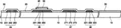
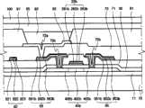
首先,将参照图6A和图6B来描述包括上述布线结构的根据本发明实施例的薄膜晶体管(TFT)基板。图6A是示出了根据本发明实施例的薄膜晶体管(TFT)基板的布局图,以及图6B是沿着图6A中的线B-B’截取的截面图。First, a thin film transistor (TFT) substrate according to an embodiment of the present invention including the above wiring structure will be described with reference to FIGS. 6A and 6B . 6A is a layout view showing a thin film transistor (TFT) substrate according to an embodiment of the present invention, and FIG. 6B is a cross-sectional view taken along line B-B' in FIG. 6A.
如图6A和图6B所示,传输选通信号的多个栅极布线形成在绝缘基板10上。栅极布线包括:栅极线22,在横向方向延伸;栅极焊盘24,连接至栅极线22的端部以接收来自外部电路(未示出)的选通信号。TFT的栅电极26连接至栅极线22。存储电极27和存储电极线28并行于栅极线22形成。存储电极线28在横向方向上延伸穿过像素区,并且连接至比存储电极线28宽的存储电极27。存储电极27覆盖与像素电极82连接的漏电极延伸部67。如下面将要描述的,这种重叠结构形成存储电容器,其增强了像素的电荷存储能力。可以使用各种形状和布置的存储电极线28和存储电极27。当通过重叠像素电极82和栅极线22而生成足够的存储电容时,可以省略形成存储电极27。As shown in FIGS. 6A and 6B , a plurality of gate wirings that transmit gate signals are formed on the insulating
如图6B所示,栅极布线22、24、26和27具有三层结构,分别包括:包含氮化铜的阻隔层221、241、261、和271,包含铜或铜合金的导电层222、242、262和272,以及保护层223、243、263和273。尽管在附图中没有直接示出,存储电极线28具有与栅极布线22、24、26和27相同的多层结构。在以下描述的具有多层结构的栅极布线中,同样包括存储电极线28,并且栅极布线22、24、26和27的多层特性同样适用于存储电极线28。As shown in FIG. 6B, the gate wirings 22, 24, 26, and 27 have a three-layer structure, respectively including: barrier layers 221, 241, 261, and 271 containing copper nitride, a
根据本发明实施例的布线结构可以应用于多层栅极布线22、24、26和27。这里,阻隔层221、241、261、和271帮助下部导电层222、242、262和272粘附到绝缘基板10并且防止形成绝缘基板10的材料和形成导电层222、242、262和272的材料彼此扩散。The wiring structure according to the embodiment of the present invention can be applied to the
栅极绝缘层30由氮化硅(SiNx)形成在基板10和栅极布线22、24、26、27和28上。半导体层40由氢化非晶硅或多晶硅以岛状形成在栅电极26上的栅极绝缘层30上。欧姆接触层55和56形成在半导体层40上,并且可以由硅化物或掺杂有高浓度n型杂质的n+氢化非晶硅制成。A
数据布线形成在欧姆接触层55和56以及栅极绝缘层30上。数据线包括:数据线62大致在纵向方向延伸并且与栅极线22交叉以限定像素;源电极65,连接至数据线62,并且在欧姆接触层55上方延伸;数据焊盘68,连接至数据线62的端部,并且接收来自外部电路的图像信号;漏电极66,与源电极65隔开,并且形成在欧姆接触层56上,由栅电极26看来与源电极65相对;以及漏电极延伸部67,从漏电极66延伸,并且具有与存储电极27重叠的大面积。Data wiring is formed on the ohmic contact layers 55 and 56 and the
与栅极布线22、24、26和27一样,数据布线62、65、66、67和68形成为三层结构,分别包括:包含氮化铜的阻隔层621、651、661、671和681,包含铜或铜合金的导电层622、642、662、672和682以及保护层623、643、663、673、和683。根据本发明实施例的布线结构应用于由多层结构形成的数据布线62、65、66、67和68。这里,阻隔层621、651、661、671和681补充了导电层622、642、662、672和682与基板的粘附度,即,欧姆接触层55和56以及栅极绝缘层30防止形成欧姆接触层55和56的材料、形成栅极绝缘层30的材料以及形成导电层622、642、662、672和682的材料彼此扩散。Like the gate wirings 22, 24, 26, and 27, the data wirings 62, 65, 66, 67, and 68 are formed in a three-layer structure including: barrier layers 621, 651, 661, 671, and 681 containing copper nitride, respectively, Conductive layers 622 , 642 , 662 , 672 , and 682 and
源电极65与至少部分的半导体层40重叠。漏电极66从栅电极26看过来与源电极65相对并面向源电极,并且与至少部分的半导体层40重叠。欧姆接触层55和56存在于下部半导体层40和上部源电极65以及漏电极66之间,以减小其之间的接触电阻。The source electrode 65 overlaps at least part of the
漏电极延伸部67与存储电极27重叠,以形成将栅极绝缘层30插入存储电极27和漏电极延伸部67之间的存储电极器。在没有存储电极27的情况下,可以不形成漏电极延伸部67。The
这里,栅电极26、形成于其上的半导体层40、欧姆接触层55和56、源电极65、以及漏电极66构成TFT,并且半导体层40构成TFT的沟道区。在示出的本发明的实施例中,采用了底部栅极型TFT,其中,栅电极26形成在包括沟道区的半导体层40的下面。Here, the
钝化层70形成在数据线62、65、66、67和68以及从其穿过的半导体层40的露出部上。钝化层70可以优选地由具有良好平特性(flatness characteristic)的感光有机材料、诸如通过等离子体增强化学汽相沉积(PECVD)形成的低介电绝缘材料(例如,a-Si:C:O和a-Si:O:F)、或诸如氮化硅的无机绝缘体制成。当钝化层70由有机材料制成时,由氮化硅(SiN)或二氧化硅(SiO2)制成的绝缘层(未示出)可以进一步设置在有机层下面,以防止钝化层70的有机材料与源电极65和漏电极66之间的半导体层40的露出部分接触。A
接触孔77和78形成在钝化层70中,以分别露出漏电极延伸部67和数据焊盘68。接触孔74形成在钝化层70和栅极绝缘层30中,以露出栅极焊盘24。像素电极82以经由接触孔77电连接至漏电极66并且位于像素区中的方式形成在钝化层70上。像素电极82通过接触孔77在物理上电连接至漏电极66,使得像素电极82接收来自漏电极66的数据电压。在被供给数据电压的像素电极82和上显示基板的共电极之间产生电场,该电场决定了像素电极82和共电极之间的LC层中的液晶分子的方向。Contact holes 77 and 78 are formed in the
此外,辅助栅极焊盘84和辅助数据焊盘88以分别经由接触孔74和78连接至栅极焊盘24和数据焊盘68的方式形成在钝化层70上。像素电极82和辅助栅极焊盘84以及辅助数据焊盘88优选地由诸如ITO的透明导体制成。In addition, an
根据本发明实施例的TFT基板可以应用到液晶显示器(LCD)等。The TFT substrate according to an embodiment of the present invention may be applied to a liquid crystal display (LCD) or the like.
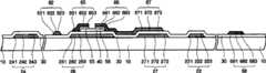
接下来,将参照图6A和图6B以及图7A至图10B来详细描述根据本发明实施例的制造TFT基板的方法。本领域技术人员将发现省略了本发明的一些特定细节。对于可以应用根据本发明实施例的用于形成布线结构的方法的部分,在本领域技术人员能够容易预见或理解具体实施例的情况下,没有论述或详细描述一些特定技术细节。图7A、8A、9A和10A是顺序地示出了根据本发明实施例的制造TFT基板的方法的布局图,以及图7B、8B、9B、和10B是沿着图7A、8A、9A和10A中的线B-B’截取的截面图。Next, a method of manufacturing a TFT substrate according to an embodiment of the present invention will be described in detail with reference to FIGS. 6A and 6B and FIGS. 7A to 10B . Those skilled in the art will find that some specific details of the invention have been omitted. For the part to which the method for forming a wiring structure according to the embodiment of the present invention can be applied, some specific technical details are not discussed or described in detail as those skilled in the art can easily foresee or understand the specific embodiment. 7A, 8A, 9A, and 10A are layout views sequentially showing a method of manufacturing a TFT substrate according to an embodiment of the present invention, and FIGS. 7B, 8B, 9B, and 10B are along the lines of FIGS. A cross-sectional view taken along line BB' in .
首先,如图7A和7B所示,通过使用溅射在绝缘基板10上顺序地沉积包括氮化铜的阻隔层221、241、261和271、包括铜或铜合金的铜导电层222、242、262和272、以及保护层223、243、263和273来形成栅极多层。然后,在栅极多层上形成限定栅极布线22、24、26、27和28的光刻胶图样,并且使用光刻胶图样作为蚀刻掩模以批处理方式顺序地蚀刻保护层223、243、263和273、铜导电层222、242、262和272、以及阻隔层221、241、261和271。光刻胶图样然后被去除。这样,形成包括栅极线22、栅电极26、栅极焊盘24、存储电极27、和存储电极线28的栅极布线。使用根据本发明实施例的制造布线的方法来形成栅极布线22、24、26、27和28。因此,如同参照图5A和5B所描述的,所形成的包括铜导电层222、242、262和272的栅极布线22、24、26、27和28被较好的附着到基板,并且即使在湿蚀刻并去除光刻胶层之后,它们的侧面轮廓也没有突出且具有良好圆锥角。First, as shown in FIGS. 7A and 7B , barrier layers 221, 241, 261, and 271 including copper nitride, copper
然后,如图8A和8B所示,使用化学汽相沉积(CVD)顺序地将由氮化硅制成的栅极绝缘层30、本质非晶硅层、以及掺杂非晶硅层分别沉积为

参照图9A和9B,通过使用溅射在栅极绝缘层30和掺杂半导体层50上顺序地沉积包括氮化铜的阻隔层621、651、661、671和681、包括铜或铜合金的导电层622、642、662、672和682、以及保护层623、643、663、673和683。在数据多层上形成限定数据布线62、65、66、67和68的光刻胶图样,并且使用光刻胶图样作为蚀刻掩模以批处理方式顺序地蚀刻保护层623、643、663、673和683、导电层622、642、662、672和682、以及阻隔层621、651、661、671和681,从而露出沟道区下面的掺杂半导体层50。然后去除光刻胶图样。形成数据布线62、65、66、67和68,数据布线62、65、66、67和68包括:数据线62,基本上在纵向方向延伸并且与栅极线22交叉;源电极65,连接至数据线62并且在欧姆接触层55之上延伸;数据焊盘68,连接至数据线62的端部并且接收来自外部电路的图像信号;漏电极66,与源电极65隔开并形成在欧姆接触层56上,以从栅电极26来看与源电极65相对;以及漏电极延伸部67,从漏电极66延伸并且具有大面积与存储电极27重叠。通过与根据本发明实施例形成布线结构的方法相同的方法来形成数据布线62、65、66、67和68。因此,如同参照图5A和5B所描述的,所形成的数据布线62、65、66、67和68较好地附着到基板,并且即使在湿蚀刻之后,它们的侧面轮廓也没有突起并且良好圆锥角。Referring to FIGS. 9A and 9B , barrier layers 621 , 651 , 661 , 671 , and 681 including copper nitride, conductive layers including copper or copper alloy are sequentially deposited on the
接下来,对通过数据布线62、65、66、67和68露出的掺杂半导体层50执行干蚀刻,从而在栅电极26的两侧形成欧姆接触层55和56,并且露出欧姆接触层55和56之间的半导体层40。此时,可以使用源电极65和66作为蚀刻掩模来执行蚀刻,并且可以在使用限定数据布线62、65、66、67和68的光刻胶图样作为蚀刻掩模来对半导体层40执行干蚀刻之后去除光刻胶图样。因此,形成了底栅极型TFT,其包括栅电极26、形成于其上的半导体层40、欧姆接触层55和56、源电极65、以及漏电极66,其中栅电极26形成在半导体层40的沟道区下面。Next, dry etching is performed on the doped
然后,如图10A和10B所示,钝化层70由单层或多层形成,其中,单层或多层由具有优异平面特性和感光性的有机材料、通过等离子体增强化学汽相沉积(PEVCD)形成的具有低介电常数的绝缘材料(例如,a-Si:C:O或a-Si:O:F)、或诸如SiNx的无机材料制成。Then, as shown in FIGS. 10A and 10B , the
接下来,通过光刻使栅极绝缘层30和钝化层70图样化,从而形成露出栅极焊盘24、漏电极延伸部67、以及数据焊盘68的接触孔74、77和78。当钝化层70由具有感光性的有机材料制成时,可以优选地在与栅极绝缘层30和钝化层70具有相同的蚀刻选择性的蚀刻条件下,仅通过光刻来形成接触孔74、77和78。Next, the
接下来,如图5A和5B所示,沉积氧化铟锡(ITO)层并且对ITO层执行光刻,从而形成通过接触孔77连接至漏电极66的像素电极82、以及通过接触孔74和78连接至栅极焊盘24和数据焊盘68的辅助栅极焊盘84和辅助数据焊盘88。Next, as shown in FIGS. 5A and 5B , an indium tin oxide (ITO) layer is deposited and photolithography is performed on the ITO layer, thereby forming a
尽管半导体层形成为岛状,以及在本发明示出的实施例中描述了具有数据布线和不同图样的TFT基板以及TFT基板的制造方法,但是本发明还可以应用于具有半导体层和相同图样布线的TFT基板以及TFT基板的制造方法,这将在下文中参照图11A和11B来描述。图11A是示出了根据本发明实施例的TFT基板的另一实例的布局图,以及图11B是沿着图11A中的线B-B’截取的截面图。Although the semiconductor layer is formed in an island shape, and a TFT substrate having data wiring and a different pattern and a manufacturing method of the TFT substrate have been described in the illustrated embodiment of the present invention, the present invention can also be applied to a TFT substrate having a semiconductor layer and the same pattern wiring. The TFT substrate and the manufacturing method of the TFT substrate will be described below with reference to FIGS. 11A and 11B . 11A is a layout view showing another example of a TFT substrate according to an embodiment of the present invention, and FIG. 11B is a cross-sectional view taken along line B-B' in FIG. 11A .
如图11A和图11B所示,除了半导体层42、44和48以及欧姆接触层52、55、56和58形成为具有与数据布线62、65、66、67和68相同图样的线性形状之外,TFT基板的修改实例具有与图6A和6B类似的结构。然而,欧姆接触层52、55、56和58具有与数据布线62、65、66、67和68基本上相同的图样,但是不同在于,半导体层44没有连接在沟道区。不同于根据本发明实施例的使用不同掩模来形成半导体层和数据布线的TFT基板的制造方法,在根据本发明另一实施例的制造TFT基板的方法中,使用包括狭缝或半透膜的单掩模来使数据布线、欧姆接触层、和数据线形成图样。由于其他处理与根据本发明实施例的制造TFT基板的方法大致相同,并且本领域技术人员可以容易地实施,因此将不再给出详细描述。11A and 11B, except that the semiconductor layers 42, 44 and 48 and the ohmic contact layers 52, 55, 56 and 58 are formed in a linear shape having the same pattern as the data wirings 62, 65, 66, 67 and 68 , the modified example of the TFT substrate has a structure similar to that of FIGS. 6A and 6B. However, the ohmic contact layers 52, 55, 56 and 58 have substantially the same pattern as the data wirings 62, 65, 66, 67 and 68, but differ in that the
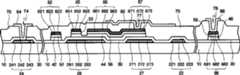
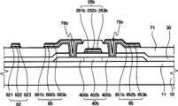
接下来,将参照图12A至12C来描述根据本发明另一实施例的TFT基板的制造方法。根据本发明另一实施例的TFT基板用于有机EL显示装置,并且包括根据本发明实施例的布线结构。至于哪些部分可以应用根据本发明实施例的布线结构制造方法,由于本领域技术人员能够容易的想象或理解,因此一些特定技术细节没有论述或详细描述。图12A是示出了根据本发明另一实施例的TFT基板的布局图,以及图12B和12C是沿着图12A中的线B-B’和C-C’截取的截面图。Next, a method of manufacturing a TFT substrate according to another embodiment of the present invention will be described with reference to FIGS. 12A to 12C. A TFT substrate according to another embodiment of the present invention is used for an organic EL display device, and includes a wiring structure according to an embodiment of the present invention. As for which parts can be applied to the manufacturing method of the wiring structure according to the embodiment of the present invention, since those skilled in the art can easily imagine or understand, some specific technical details are not discussed or described in detail. 12A is a layout view showing a TFT substrate according to another embodiment of the present invention, and FIGS. 12B and 12C are cross-sectional views taken along lines B-B' and C-C' in FIG. 12A.
由氧化硅或氮化硅制成的阻挡层11形成在绝缘基板10上,并且由多晶硅制成的第一半导体层40a和第二半导体层40b形成在阻挡层11上。由多晶硅制成的电容器半导体层40c连接至第二半导体层40b。第一半导体层40a包括第一TFT部405a、406a和402a,以及第二半导体层40b包括第二TFT部405b、406b和402b。第一TFT部405a、406a和402a的被称为第一源区的第一TFT部405a、以及被称为第一漏区的区域406a掺杂有n型杂质,第二半导体层40b的被称为第二源区的第二TFT部405b、以及被称为第二漏区的区域406b掺杂有p型杂质。根据驱动条件,第一源区405a和第一漏区406b可以掺杂有p型杂质并且第二源区405b和第二漏区406b可以掺杂有n型杂质。A
由氧化硅和氮化硅制成的栅极绝缘层30形成在半导体层40a、40b和40c上。栅极布线形成在栅极绝缘层30上,包括:栅极线22,在横向方向延伸;第一栅电极26a,以突起的形式连接至栅极线22,并且与第一TFT的沟道区402a重叠;第二栅电极26b,与栅极线22隔开,并且与第二TFT的沟道区402b重叠;以及存储电极27,连接至第二栅电极26b,并且与电容器半导体层40c重叠。A
栅极布线22、26a、26b和27具有三层结构,包括:包括氮化铜的阻隔层261a、261b和271、包括铜或铜合金的铜导电层262a、262b和272、以及保护层263a、263b和273。尽管在附图中没有直接示出,栅极线22具有与栅极布线26a、26b和27相同的多层结构。在具有以下描述的具有多层结构的栅极布线中,也包括栅极线22,并且栅极布线26a、26b和27的多层特性同样适用于栅极线22。The gate wirings 22, 26a, 26b, and 27 have a three-layer structure including:
根据本发明实施例的布线结构可以应用于多层栅极布线22、26a、26b和27。这里,阻隔层261a、261b和271帮助重叠的导电层262a、262b和272附着到栅极绝缘层30,并且防止形成栅极绝缘层30的材料和形成铜导电层262a、262b和272的材料彼此扩散。The wiring structure according to the embodiment of the present invention can be applied to the
第一层间绝缘层71形成在形成有栅极布线22、26a、26b和27的栅极绝缘层30上。The first
数据布线形成在第一层间绝缘层71上。数据布线包括:数据线62,在纵向方向延伸,与栅极线22交叉,并且限定像素;驱动电压线63,用于提供驱动电压;第一源电极65a,通过接触孔75a连接至第一源区405a作为数据线62的分支;第一漏电极66a,与第一源电极65a分开并连接到第一源区406a;第二源电极65b,通过接触孔75b连接至第二源区406b作为驱动电压线63的分支;以及第二漏电极66b,与第二源电极65b隔开,并且连接至第二漏区406b。第一漏电极66a通过穿过第一层间绝缘层71和栅极绝缘层30的接触孔76a和73与第一漏区406a和第二栅极26b接触,并与其电连接。第二漏电极66b通过穿过第一层间绝缘层71和栅极绝缘层30的接触孔76b与第二漏区406b电连接。Data wiring is formed on the first
如同栅极布线22、26a、26b和27一样,数据布线62、63、65a、65b、66a和66b具有三层结构,该三层结构分别包括:包含氮化铜的阻隔层621、631、651a、651b、661a和661b、包含铜或铜合金的铜导电层621、632、652a、652b、662a和662b、以及保护层623、643、663、673和683。Like the gate wirings 22, 26a, 26b, and 27, the data wirings 62, 63, 65a, 65b, 66a, and 66b have a three-layer structure including, respectively: barrier layers 621, 631, 651a containing copper nitride , 651b, 661a and 661b, copper
将根据本发明实施例的布线结构应用于多层数据布线62、63、65a、65b、66a和66b。这里,阻隔层621、631、651a、651b、661a和661b补充铜导电层621、632、652a、652b、662a和662b与基板的粘附度,即,半导体层405a、405b、406a和406b以及第一层间绝缘层71防止形成半导体层405a、405b、406a和406b的材料、形成第一层间绝缘层71的材料以及形成铜导电层621、632、652a、652b、662a和662b的材料相互扩散。The wiring structure according to the embodiment of the present invention is applied to the multilayer data wirings 62, 63, 65a, 65b, 66a, and 66b. Here, the barrier layers 621, 631, 651a, 651b, 661a, and 661b supplement the adhesion of the copper
这里,半导体层40a和40b、第一栅电极26a和第二栅电极26b、第一源电极65a和第二源电极65b、以及第一漏电极66a和第二漏电极66b分别构成第一TFT晶体管和第二TFT晶体管。第一TFT是开关TFT以及第二TFT是驱动TFT。在示出的实施例中,形成了顶部栅极型TFT,包括形成在具有沟道区402a和402b的半导体层40a和40b上的栅电极26a和26b。Here, the semiconductor layers 40a and 40b, the
由氮化硅、氧化硅、或有机绝缘材料制成的第二层间绝缘层72形成在数据布线62、63、65a、65b、66a和66b上,并且包括露出漏电极66b的接触孔72b。A second
通过接触孔72b连接至第二漏电极66b的像素电极82形成在第二层间绝缘层72上。像素电极82优选地由诸如Al(或Al合金)或Ag(或Ag合金)的高反射率材料制成。在必要时,像素电极82可以由诸如ITO或IZO的透明导电材料制成。形成像素电极82的材料可以根据显示装置是在TFT基板以下显示图像的底部发光型还是在TFT基板以上显示图像的顶部发光型来适当地选择。A
由有机绝缘材料制成的隔墙91形成在第二层间绝缘层72上,以隔开有机发光单元。通过曝光和显影包括黑色颜料的感光剂来形成隔墙91以作为阻挡层,并且简化其形成过程。有机发光层92形成在被隔墙91围绕的像素电极82上的区域中。由发射红色、绿色、和蓝色光中的一种的有机层制成的有机发光层92以及有机发光层92的红色、绿色、和蓝色有机层重复地顺序设置。A
缓冲层95形成在有机发光层92和隔墙91上。如果必要可以不形成缓冲层95。The
共电极100形成在缓冲层95上。共电极100由诸如ITO或IZO的透明导电材料制成。当像素电极82可以由诸如ITO或IZO的透明导电材料制成时,共电极100可以由诸如Al(或Al合金)或Ag(或Ag合金)的高反射率材料制成。The
根据本发明另一实施例的TFT基板可以应用于有机EL显示装置。A TFT substrate according to another embodiment of the present invention may be applied to an organic EL display device.
接下来,将参照图12A至12C和图13A至18C来详细描述根据本发明另一实施例的TFT基板制造方法。对于可以应用根据本发明实施例的形成布线结构的方法的部分,因为本领域技术人员能够容易预见或理解具体实施例,所以没有论述或详细描述一些特定技术细节。图13A、14A、15A、16A、17A、和18A是顺序示出根据本发明另一实施例的制造TFT基板的方法的布局图,以及图13B、14B、15B、16B、17B、和18B是沿着示出了处理步骤的图13A、14A、15A、16A、17A、和18A中的线B-B’截取的截面图,以及图13C、14C、15C、16C、17C、和18C是沿着示出了处理步骤的图13A、14A、15A、16A、17A、和18A中的线C-C’截取的截面图。Next, a TFT substrate manufacturing method according to another embodiment of the present invention will be described in detail with reference to FIGS. 12A to 12C and FIGS. 13A to 18C. For the part to which the method of forming a wiring structure according to the embodiment of the present invention can be applied, some specific technical details are not discussed or described in detail because those skilled in the art can easily foresee or understand the specific embodiment. 13A, 14A, 15A, 16A, 17A, and 18A are layout views sequentially showing a method of manufacturing a TFT substrate according to another embodiment of the present invention, and FIGS. Figures 13A, 14A, 15A, 16A, 17A, and 18A are cross-sectional views taken along line BB' showing process steps, and Figures 13C, 14C, 15C, 16C, 17C, and 18C are along the lines shown Cross-sectional views taken along line CC' in Figures 13A, 14A, 15A, 16A, 17A, and 18A illustrate the processing steps.
参照图13A至13C,通过将氧化硅沉积在基板10上来形成阻挡层11,并且通过低压化学汽相沉积(LPCVD)或等离子体增强化学汽相沉积(PECVD)将非晶硅沉积在阻挡层11上,然后被图样化。接下来,用激光照射非晶硅或对其施热,以将非晶硅结晶成多晶硅。接下来,形成由多晶硅制成的半导体层40a、40b和40c。Referring to FIGS. 13A to 13C, the
参照图14A至14C,栅极绝缘层30形成在阻挡层11上,半导体层40a、40b和40c通过使用CVD沉积氮化硅而形成在阻挡层处。14A to 14C, a
通过使用溅射在栅极绝缘层30上顺序沉积包括氮化铜的阻隔层261a、261b和271、包括铜或铜合金的铜导电层262a、262b和272、以及保护层263a、263b和273来形成栅极多层。By sequentially depositing
接下来,用于限定第一栅电极26a和栅极线22的第一光刻胶图样形成在栅极多层上。覆盖和保护将要形成第二栅电极26b和存储电极27的区域,其包括第二TFT的沟道区402b。然后,使用第一光刻胶图样作为蚀刻掩模来顺序蚀刻或以批处理方式蚀刻保护层263a、铜导电层262a、以及阻隔层261a。Next, a first photoresist pattern for defining the
通过在第一TFT部的半导体层40a中注入n型杂质离子来限定第一栅电极26a下面的沟道区402a,并且形成第一源区405a和第一漏区406a。然后,去除第一光刻胶图样。因此,形成了栅极线22、第一栅电极26a以及包括沟道区402a、第一源区405a、以及第一漏区406a的半导体层40a。A
接下来,形成用于限定第二栅电极26b和存储电极27的第二光刻胶图样。覆盖和保护形成第一栅电极26a和栅极线22的区域,其包括第一TFT的沟道区402a。然后,使用第二光刻胶图样作为蚀刻掩模来顺序蚀刻或以批处理方式蚀刻保护层263b和273、铜导电层262b和272、以及阻隔层261b和271。Next, a second photoresist pattern for defining the
通过向第二TFT部的半导体层40b注入p型杂质来限定第二栅电极26b下面的沟道区402b,并且形成第二源区405b和第二漏区406b。接下来,去除第二光刻胶图样。因此,形成第二栅电极26b、存储电极27、以及包括沟道区402b、第二源区405b、以及第二漏区406b的半导体层40b。A
根据本发明实施例的布线结构可以应用于栅极布线22、26a、26b和27。因此,如图5A和5B所示,即使在诸如湿蚀刻以及去除光刻胶层的图样化处理之后,所形成的包括铜导电层262a、262b和272的栅极布线22、26a、26b和27也能较好地附着于基板。另外,布线结构的侧面轮廓没有突起并且具有良好圆锥角。The wiring structure according to the embodiment of the present invention can be applied to the gate wirings 22 , 26 a , 26 b and 27 . Therefore, as shown in FIGS. 5A and 5B, even after patterning processes such as wet etching and removal of the photoresist layer, the formed
参照图15A至15C,在形成有栅极布线22、26a、26b和27的栅极绝缘层30上沉积第一层间绝缘层71,并且对第一层间绝缘层71和栅极绝缘层30执行光刻,从而形成露出第一源区405a、第一漏区406a、第二源区405b、以及第二漏区406的接触孔75a、76a、75b和76b以及漏出第二栅电极26b的一部分的接触孔73。Referring to FIGS. 15A to 15C, a first
参照图16A至16C,通过使用溅射,在由第一层间绝缘层71和接触孔75a、76a、75b和76b露出的半导体层40a和40b上顺序沉积包括氮化铜的阻隔层621、631、651a、651b、661a和661b、包括铜或铜合金的铜导电层622、632、652a、652b、662a和662b、以及保护层623、633、653a、653b、663a和663b来形成数据多层。接下来,在数据多层上形成用于限定数据布线的光刻胶图样,并且使用光刻胶图样作为蚀刻掩模来顺序蚀刻或以批处理方式蚀刻保护层623、633、653a、653b、663a和663b、铜导电层622、632、652a、652b、662a和662b、以及阻隔层621、631、651a、651b、661a和661b。形成数据布线,其包括:数据线62,在纵向方向延伸,与栅极线22交叉以限定像素;驱动电压线63,提供驱动电压;第一源电极65a,通过接触孔75a连接至第一源极区405a作为数据线62的分支;第一漏电极66a,与第一源电极65a隔开,并且连接至第一漏区406a;第二源电极65b,通过接触孔75b连接至第二源区406a作为驱动电压线63的分支;以及第二漏电极66b,与第二源电极65b隔开,并且连接至第二漏区406b。根据本发明实施例的布线结构可以应用于数据布线62、63、65a、65b、66a和66b。因此,如图5A和5B所示,即使在诸如湿蚀刻以及去除光刻胶层的图样化处理之后,所形成的包括铜导电层622、632、652a、652b、662a和662b的数据布线62、63、65a、65b、66a和66b也能较好地附着到基板。另外,布线结构的侧面轮廓没有突起并且具有良好圆锥角。因此,形成了包括半导体层40a、形成于其上的栅电极26a、源电极65a、以及漏电极66a的第一顶部栅极型TFT,其中,栅电极26a形成在半导体层40a上,以及形成了包括半导体层40b、形成于其上的栅电极26b、源电极65b、以及漏电极66b的第二顶部栅极型TFT,其中,栅电极26b形成在半导体层40b上。Referring to FIGS. 16A to 16C, by using sputtering, barrier layers 621, 631 including copper nitride are sequentially deposited on the semiconductor layers 40a and 40b exposed by the first
接下来,如图17A至17C所示,沉积第二层间绝缘层72并使其图样化,从而形成露出第二漏电极66b的接触孔72b。Next, as shown in FIGS. 17A to 17C, the second
然后,如图18A至18C所示,沉积并取样化诸如铝(或铝合金)或银(或银合金)的具有优异反射率的金属,从而形成像素电极82。Then, as shown in FIGS. 18A to 18C , a metal having excellent reflectivity such as aluminum (or aluminum alloy) or silver (or silver alloy) is deposited and sampled, thereby forming the
然后,如图12A至12C所示,将包括黑色颜料的有机层涂布在形成有像素电极82的第二层间绝缘层72上,然后将其曝光并显影,从而形成填充除了有机发光空间之外的区域的隔墙91。接下来,使用沉积或喷墨印刷,在有机发光空间中形成有机发光层92。Then, as shown in FIGS. 12A to 12C , an organic layer including a black pigment is coated on the second
之后,在隔墙91和有机发光层92上涂布导电有机材料,从而形成缓冲层95。在缓冲层95上沉积ITO或IZO,从而形成共电极100。这里,像素电极82优选地由诸如ITO或IZO的透明导电材料制成。在这种情况下,共电极100可以由诸如Al(或Al合金)或Ag(或Ag合金)的高反射率材料制成。Thereafter, a conductive organic material is coated on the
虽然已经通过实例的方式在根据本发明多个实施例的TFT基板及其制造方法中描述了包括在栅极线和数据线中包含氮化铜的阻隔层、包含铜或铜合金的铜导电层、以及保护层的三层布线结构,然而栅极线和数据线中可能只有一个具有三层布线结构而另一个可以具有本领域内已知的布线结构或者本发明范围内的任何其他特定布线结构。Although it has been described by way of example in the TFT substrate and the manufacturing method thereof according to various embodiments of the present invention that the barrier layer including copper nitride in the gate line and the data line, the copper conductive layer including copper or copper alloy , and a three-layer wiring structure of the protective layer, however, only one of the gate line and the data line may have a three-layer wiring structure and the other may have a wiring structure known in the art or any other specific wiring structure within the scope of the present invention .
虽然上述的根据本发明实施例的TFT基板及其制造方法通过实例的方式应用于底部栅极型LCD,但是本发明并不局限于此,其还可以应用于有机EL显示器。在这种情况下,为每个像素设置一对底部栅极型TFT分别作为开关TFT和驱动TFT。同时,虽然上述的根据本发明另一实施例的TFT基板及其制造方法通过实例的方式应用于顶部栅极型有机EL显示器,但是本发明并不局限于此,其还可以应用于具有用于每个像素的TFT的LCD的TFT基板。在这种情况下,顶部栅极型TFT LCD优选地是反射型。除了示出的实施例之外,根据本发明的TFT基板及其制造方法可以有利地应用于在滤色器上具有薄膜晶体管的滤色器(AOC)基板上的阵列。此外,根据本发明的TFT基板及其制造方法可以应用于各种TFT基板,并且没有给出其详细描述,以便不会不必要地使本发明的各个方面模糊。Although the above-mentioned TFT substrate and its manufacturing method according to the embodiments of the present invention are applied to a bottom gate type LCD by way of example, the present invention is not limited thereto and can also be applied to an organic EL display. In this case, a pair of bottom gate type TFTs are provided for each pixel as a switching TFT and a driving TFT, respectively. Meanwhile, although the above-mentioned TFT substrate and its manufacturing method according to another embodiment of the present invention are applied to a top gate type organic EL display by way of example, the present invention is not limited thereto, and it can also be applied to a display having a top gate type. LCD TFT substrate with TFT for each pixel. In this case, the top gate type TFT LCD is preferably a reflective type. In addition to the illustrated embodiments, the TFT substrate and manufacturing method thereof according to the present invention may be advantageously applied to an array on an color filter (AOC) substrate having thin film transistors on a color filter. Also, the TFT substrate and method of manufacturing the same according to the present invention can be applied to various TFT substrates, and a detailed description thereof is not given so as not to unnecessarily obscure aspects of the present invention.
如上所述,在根据本发明的布线结构和制造布线结构的方法中,改善了铜导电层到基板的粘附度,并且可以获得具有改善的侧面轮廓和可靠性的低阻抗铜布线。As described above, in the wiring structure and the method of manufacturing the wiring structure according to the present invention, the degree of adhesion of the copper conductive layer to the substrate is improved, and low-resistance copper wiring with improved side profile and reliability can be obtained.
另外,简化了制造布线结构的方法并且提高了处理效率。In addition, the method of manufacturing the wiring structure is simplified and processing efficiency is improved.
此外,在根据本发明的TFT基板和制造TFT基板的方法中,可以确保栅极布线和/或数据布线的优异可靠性,从而改善信号特性、图像质量、以及处理效率。Furthermore, in the TFT substrate and the method of manufacturing the TFT substrate according to the present invention, excellent reliability of gate wiring and/or data wiring can be ensured, thereby improving signal characteristics, image quality, and processing efficiency.
在总结对本发明的详细描述时,本领域技术人员可以理解,在不背离本发明的精神的情况下,可以对优选实施例作出各种修改和变化。因此,所公开的本发明的优选实施例仅是一般性的和描述性的,而不是用于限制本发明。Having concluded the detailed description of the invention, those skilled in the art will appreciate that various modifications and changes can be made to the preferred embodiment without departing from the spirit of the invention. Accordingly, the disclosed preferred embodiments of the invention are generic and descriptive only, and are not intended to be limiting of the invention.
Claims (15)


Applications Claiming Priority (3)
| Application Number | Priority Date | Filing Date | Title |
|---|---|---|---|
| KR1020050064483 | 2005-07-15 | ||
| KR1020050064483AKR101168728B1 (en) | 2005-07-15 | 2005-07-15 | Wire and method for fabricating interconnection line and thin film transistor substrate and method for fabricating the same |
| KR10-2005-0064483 | 2005-07-15 |
Publications (2)
| Publication Number | Publication Date |
|---|---|
| CN1897270A CN1897270A (en) | 2007-01-17 |
| CN1897270Btrue CN1897270B (en) | 2011-08-17 |
Family
ID=37609722
Family Applications (1)
| Application Number | Title | Priority Date | Filing Date |
|---|---|---|---|
| CN200610099012XAExpired - Fee RelatedCN1897270B (en) | 2005-07-15 | 2006-07-12 | Wiring structure, method of manufacturing wiring, thin film transistor substrate and method of manufacturing the same |
Country Status (4)
| Country | Link |
|---|---|
| US (2) | US7851920B2 (en) |
| KR (1) | KR101168728B1 (en) |
| CN (1) | CN1897270B (en) |
| TW (1) | TWI396885B (en) |
Families Citing this family (28)
| Publication number | Priority date | Publication date | Assignee | Title |
|---|---|---|---|---|
| KR20080008562A (en)* | 2006-07-20 | 2008-01-24 | 삼성전자주식회사 | Manufacturing Method of Array Substrate, Array Substrate and Display Device Having Same |
| CN102097472A (en)* | 2006-12-28 | 2011-06-15 | 株式会社爱发科 | Process for forming a wiring film, a transistor, and an electronic device |
| KR20080084084A (en)* | 2007-03-14 | 2008-09-19 | 엘지디스플레이 주식회사 | Method of manufacturing thin film transistor and array substrate for liquid crystal display device comprising same |
| KR101308534B1 (en)* | 2007-07-18 | 2013-09-23 | 삼성디스플레이 주식회사 | Display substrate and method for manufacturing the same |
| JP5377940B2 (en)* | 2007-12-03 | 2013-12-25 | 株式会社半導体エネルギー研究所 | Semiconductor device |
| KR101414043B1 (en)* | 2007-12-04 | 2014-07-21 | 삼성디스플레이 주식회사 | Thin film transistor substrate |
| KR101253497B1 (en)* | 2008-06-02 | 2013-04-11 | 엘지디스플레이 주식회사 | Method of fabricating array substrate for liquid crystal display device |
| WO2010010753A1 (en)* | 2008-07-22 | 2010-01-28 | 国立大学法人東北大学 | Wiring board and method for manufacturing the same |
| TWI405017B (en)* | 2008-12-18 | 2013-08-11 | Lg Display Co Ltd | Array substrate of display device and manufacturing method thereof |
| JP5502996B2 (en)* | 2010-05-27 | 2014-05-28 | パナソニック株式会社 | Thin film semiconductor device, display device, and method of manufacturing thin film semiconductor device |
| TWI471946B (en)* | 2010-11-17 | 2015-02-01 | Innolux Corp | Thin film transistor |
| CN102254950B (en)* | 2011-07-12 | 2013-05-08 | 北京大学深圳研究生院 | Cuprous oxide thin film transistor and preparing method thereof |
| JP5781428B2 (en)* | 2011-12-20 | 2015-09-24 | 日東電工株式会社 | Conductive film and conductive film roll |
| KR101968115B1 (en) | 2012-04-23 | 2019-08-13 | 엘지디스플레이 주식회사 | Array substrate and method of fabricating the same |
| US8859419B2 (en) | 2013-02-01 | 2014-10-14 | Globalfoundries Inc. | Methods of forming copper-based nitride liner/passivation layers for conductive copper structures and the resulting device |
| US8753975B1 (en) | 2013-02-01 | 2014-06-17 | Globalfoundries Inc. | Methods of forming conductive copper-based structures using a copper-based nitride seed layer without a barrier layer and the resulting device |
| CN103227208B (en)* | 2013-04-10 | 2016-12-28 | 京东方科技集团股份有限公司 | Thin film transistor (TFT) and manufacture method, array base palte and display device |
| KR102044667B1 (en)* | 2013-05-28 | 2019-11-14 | 엘지디스플레이 주식회사 | Flat panel display device having oxide thin film transistor and method for fabricating thereof |
| US9293480B2 (en)* | 2013-07-10 | 2016-03-22 | Semiconductor Energy Laboratory Co., Ltd. | Semiconductor device and display device including the semiconductor device |
| TWI551926B (en) | 2014-01-27 | 2016-10-01 | 友達光電股份有限公司 | Pixel structure |
| CN104600123B (en) | 2015-01-05 | 2018-06-26 | 京东方科技集团股份有限公司 | A kind of thin film transistor (TFT) and preparation method thereof, array substrate and display device |
| CN105185840A (en)* | 2015-10-28 | 2015-12-23 | 深圳市华星光电技术有限公司 | Thin-film transistor, array substrate and production method thereof |
| CN114068724A (en)* | 2016-01-29 | 2022-02-18 | 株式会社半导体能源研究所 | Semiconductor device and transistor |
| US10483285B2 (en) | 2016-06-01 | 2019-11-19 | Innolux Corporation | Element substrate and display device |
| KR102839408B1 (en)* | 2019-01-17 | 2025-07-28 | 삼성디스플레이 주식회사 | Display devices and manufacturing method thereof |
| CN111403336A (en)* | 2020-03-31 | 2020-07-10 | 成都中电熊猫显示科技有限公司 | Array substrate, display panel and manufacturing method of array substrate |
| KR102848665B1 (en)* | 2020-04-27 | 2025-08-25 | 삼성디스플레이 주식회사 | Display device |
| CN114695529B (en)* | 2022-03-16 | 2025-01-28 | Tcl华星光电技术有限公司 | TFT substrate and manufacturing method thereof, liquid crystal display panel and OLED display panel |
Citations (2)
| Publication number | Priority date | Publication date | Assignee | Title |
|---|---|---|---|---|
| CN1167420A (en)* | 1996-04-25 | 1997-12-10 | Lg电子株式会社 | Electrode for plasma display panel and manufacturing method thereof |
| CN1610859A (en)* | 2002-01-02 | 2005-04-27 | 三星电子株式会社 | Wiring structure, thin film transistor substrate using the wiring structure and manufacturing method thereof |
Family Cites Families (14)
| Publication number | Priority date | Publication date | Assignee | Title |
|---|---|---|---|---|
| US6219125B1 (en)* | 1996-07-26 | 2001-04-17 | Canon Kabushiki Kaisha | Electrode plate, process for producing the plate, for an LCD having a laminated electrode with a metal nitride layer |
| JP3916334B2 (en) | 1999-01-13 | 2007-05-16 | シャープ株式会社 | Thin film transistor |
| JP2000275663A (en)* | 1999-03-26 | 2000-10-06 | Hitachi Ltd | Liquid crystal display device and manufacturing method thereof |
| JP2001291720A (en)* | 2000-04-05 | 2001-10-19 | Hitachi Ltd | Semiconductor integrated circuit device and method of manufacturing semiconductor integrated circuit device |
| TW490857B (en)* | 2001-02-05 | 2002-06-11 | Samsung Electronics Co Ltd | Thin film transistor array substrate for liquid crystal display and method of fabricating same |
| TW550707B (en)* | 2001-04-27 | 2003-09-01 | Promos Technologies Inc | Tantalum carbide nitride diffusion barrier for copper metallization process |
| CN1277601C (en)* | 2001-12-21 | 2006-10-04 | 三菱化学株式会社 | Apparatus and method for processing easily polymerizable substances, apparatus for extracting liquids from decompressed apparatus, and method for preparing easily polymerizable substances |
| KR100904524B1 (en)* | 2002-12-31 | 2009-06-25 | 엘지디스플레이 주식회사 | Manufacturing method of array substrate for liquid crystal display device |
| KR100938885B1 (en) | 2003-06-30 | 2010-01-27 | 엘지디스플레이 주식회사 | Array substrate for LCD and manufacturing method |
| KR100939560B1 (en) | 2003-06-30 | 2010-01-29 | 엘지디스플레이 주식회사 | Array substrate for LCD and manufacturing method |
| TWI242289B (en)* | 2004-11-22 | 2005-10-21 | Au Optronics Corp | Fabrication method of thin film transistor |
| TWI242290B (en)* | 2004-11-22 | 2005-10-21 | Au Optronics Corp | Fabrication method of thin film transistor |
| US20060197089A1 (en)* | 2005-03-03 | 2006-09-07 | Chunghwa Picture Tubes., Ltd. | Semiconductor device and its manufacturing method |
| TWI354350B (en)* | 2005-05-25 | 2011-12-11 | Au Optronics Corp | Copper gate electrode and fabricating method there |
- 2005
- 2005-07-15KRKR1020050064483Apatent/KR101168728B1/ennot_activeExpired - Fee Related
- 2006
- 2006-06-12TWTW095120740Apatent/TWI396885B/ennot_activeIP Right Cessation
- 2006-07-12CNCN200610099012XApatent/CN1897270B/ennot_activeExpired - Fee Related
- 2006-07-15USUS11/486,720patent/US7851920B2/enactiveActive
- 2010
- 2010-11-09USUS12/942,910patent/US8158499B2/ennot_activeExpired - Fee Related
Patent Citations (2)
| Publication number | Priority date | Publication date | Assignee | Title |
|---|---|---|---|---|
| CN1167420A (en)* | 1996-04-25 | 1997-12-10 | Lg电子株式会社 | Electrode for plasma display panel and manufacturing method thereof |
| CN1610859A (en)* | 2002-01-02 | 2005-04-27 | 三星电子株式会社 | Wiring structure, thin film transistor substrate using the wiring structure and manufacturing method thereof |
Also Published As
| Publication number | Publication date |
|---|---|
| KR20070009325A (en) | 2007-01-18 |
| US20110047792A1 (en) | 2011-03-03 |
| US7851920B2 (en) | 2010-12-14 |
| KR101168728B1 (en) | 2012-07-26 |
| CN1897270A (en) | 2007-01-17 |
| TWI396885B (en) | 2013-05-21 |
| TW200705017A (en) | 2007-02-01 |
| US20070013078A1 (en) | 2007-01-18 |
| US8158499B2 (en) | 2012-04-17 |
Similar Documents
| Publication | Publication Date | Title |
|---|---|---|
| CN1897270B (en) | Wiring structure, method of manufacturing wiring, thin film transistor substrate and method of manufacturing the same | |
| US7586197B2 (en) | Wire structure, method of forming wire, thin film transistor substrate, and method of manufacturing thin film transistor substrate | |
| US7608494B2 (en) | Thin film transistor array panel and a method for manufacturing the same | |
| US9431426B2 (en) | Thin film transistor array panel including layered line structure and method for manufacturing the same | |
| CN1917202B (en) | Wiring structure, wiring manufacturing method, thin film transistor substrate and manufacturing method thereof | |
| US7808108B2 (en) | Thin film conductor and method of fabrication | |
| US20090002587A1 (en) | Thin film transistor array panel and a manufacturing method thereof | |
| JP5214125B2 (en) | Wiring structure, wiring forming method, thin film transistor substrate and manufacturing method thereof | |
| US20070015319A1 (en) | Method for forming contact hole and method for fabricating thin film transistor plate using the same | |
| KR101046928B1 (en) | Thin film transistor array panel and manufacturing method | |
| KR20120075048A (en) | Thin film transistor substrate and method for manufacturing thereof | |
| US20080268586A1 (en) | Switching device for a pixel electrode and methods for fabricating the same | |
| CN100446260C (en) | TFT array panel and its manufacturing method | |
| KR102338190B1 (en) | Thin film transistor array panel, liquid crystal display including the same, and method manufacturing the panel | |
| JP4495428B2 (en) | Method for forming thin film transistor | |
| JP2776336B2 (en) | Thin film transistor and method of manufacturing thin film transistor | |
| US20210217978A1 (en) | Transistor array | |
| KR20050075520A (en) | Method of forming multi-layer wiring in tft lcd substrate and tft lcd substrate thereby | |
| KR20070018287A (en) | Wiring structure, wiring formation method, thin film transistor substrate and manufacturing method thereof |
Legal Events
| Date | Code | Title | Description |
|---|---|---|---|
| C06 | Publication | ||
| PB01 | Publication | ||
| C10 | Entry into substantive examination | ||
| SE01 | Entry into force of request for substantive examination | ||
| C14 | Grant of patent or utility model | ||
| GR01 | Patent grant | ||
| ASS | Succession or assignment of patent right | Owner name:SAMSUNG DISPLAY CO., LTD. Free format text:FORMER OWNER: SAMSUNG ELECTRONICS CO., LTD. Effective date:20130104 | |
| C41 | Transfer of patent application or patent right or utility model | ||
| TR01 | Transfer of patent right | Effective date of registration:20130104 Address after:Gyeonggi Do, South Korea Patentee after:Samsung Display Co.,Ltd. Address before:Gyeonggi Do, South Korea Patentee before:Samsung Electronics Co.,Ltd. | |
| CF01 | Termination of patent right due to non-payment of annual fee | ||
| CF01 | Termination of patent right due to non-payment of annual fee | Granted publication date:20110817 Termination date:20210712 |