CN1897225A - Methods of Thinning Wafers - Google Patents
Methods of Thinning WafersDownload PDFInfo
- Publication number
- CN1897225A CN1897225ACN 200510083342CN200510083342ACN1897225ACN 1897225 ACN1897225 ACN 1897225ACN 200510083342CN200510083342CN 200510083342CN 200510083342 ACN200510083342 ACN 200510083342ACN 1897225 ACN1897225 ACN 1897225A
- Authority
- CN
- China
- Prior art keywords
- wafer
- thinning
- thinning technology
- bearing
- thickness
- Prior art date
- Legal status (The legal status is an assumption and is not a legal conclusion. Google has not performed a legal analysis and makes no representation as to the accuracy of the status listed.)
- Pending
Links
- 238000000034methodMethods0.000titleclaimsabstractdescription78
- 235000012431wafersNutrition0.000titledescription87
- 238000000926separation methodMethods0.000claimsdescription6
- 238000001312dry etchingMethods0.000claimsdescription4
- 229920002120photoresistant polymerPolymers0.000claimsdescription3
- 239000000463materialSubstances0.000description6
- 238000000227grindingMethods0.000description4
- 238000005530etchingMethods0.000description3
- 239000004065semiconductorSubstances0.000description3
- 238000012546transferMethods0.000description3
- 238000004140cleaningMethods0.000description2
- 238000010586diagramMethods0.000description2
- 238000001035dryingMethods0.000description2
- 238000004519manufacturing processMethods0.000description2
- 238000001020plasma etchingMethods0.000description2
- 239000000126substanceSubstances0.000description2
- 239000000919ceramicSubstances0.000description1
- 238000003486chemical etchingMethods0.000description1
- 239000011521glassSubstances0.000description1
- 238000010438heat treatmentMethods0.000description1
- 230000001678irradiating effectEffects0.000description1
- 238000012986modificationMethods0.000description1
- 230000004048modificationEffects0.000description1
- 239000013618particulate matterSubstances0.000description1
- 238000005498polishingMethods0.000description1
- 238000007517polishing processMethods0.000description1
- 238000012545processingMethods0.000description1
- 239000010453quartzSubstances0.000description1
- 238000011160researchMethods0.000description1
- VYPSYNLAJGMNEJ-UHFFFAOYSA-Nsilicon dioxideInorganic materialsO=[Si]=OVYPSYNLAJGMNEJ-UHFFFAOYSA-N0.000description1
- 238000001039wet etchingMethods0.000description1
Images


Landscapes
- Mechanical Treatment Of Semiconductor (AREA)
Abstract
Description
Translated fromChinese技术领域technical field
本发明涉及一种薄化晶片的方法,特别是涉及一种先利用一可移除的接合媒介将一晶片接合于一承载晶片上,再进行一晶片薄化工艺薄化晶片厚度的方法,藉此晶片厚度可达到100微米之下。The invention relates to a method for thinning a wafer, in particular to a method for firstly bonding a wafer to a carrier wafer by using a removable bonding medium, and then performing a wafer thinning process to thin the thickness of the wafer. The wafer thickness can reach below 100 microns.
背景技术Background technique
许多半导体元件与微机电元件,基于功能考量或是尺寸需求,必须进行晶片薄化工艺,以将晶片缩减至适当厚度。现行晶片薄化工艺以研磨(polish)与蚀刻工艺为主,而对于上述任一种方法而言,晶片厚度的极限仅能达到约100微米。一般而言,晶片薄化工艺可于制作元件之前进行,或是待元件制作完成后再由晶片的背面进行。对于前者的作法而言,当晶片厚度低于100微米以下时(一般称之为超薄晶片),过薄的厚度使晶片在固定于传送上产生问题,因而易造成晶片破裂。对于后者的作法而言,不仅同样具有晶片不易固定于传送的问题,同时在元件已制作于晶片的正面的情况下,使用研磨方式易造成元件应力改变问题,而使用蚀刻方式则易于蚀刻工艺本身以及后续清洗工艺时造成元件受损等问题。Many semiconductor components and micro-electromechanical components must perform a wafer thinning process to reduce the wafer to an appropriate thickness based on functional considerations or size requirements. The current wafer thinning process is mainly based on polishing and etching processes, and for any of the above methods, the limit of wafer thickness can only reach about 100 microns. Generally speaking, the wafer thinning process can be performed before the device is manufactured, or it can be performed on the backside of the wafer after the device is manufactured. For the former method, when the thickness of the wafer is less than 100 microns (generally referred to as ultra-thin wafer), the too thin thickness will cause problems in fixing the wafer on the transfer, thus easily causing the wafer to break. For the latter method, not only the same problem that the wafer is not easy to be fixed on the transfer, but at the same time, when the components have been fabricated on the front side of the wafer, the use of grinding will easily cause the problem of component stress change, while the use of etching will facilitate the etching process. Problems such as damage to components caused by itself and subsequent cleaning processes.
由上述可知,现有薄化晶片的方法在应用上有其极限,已无法满足现今对晶片厚度的要求,而犹待进一步的改善。鉴于此,申请人根据此缺点及依据多年相关经验,悉心观察且研究而提出改良的本发明,以提高晶片薄化工艺的极限。From the above, it can be seen that the existing methods for thinning wafers have their limitations in application, and cannot meet the current requirements for wafer thickness, and further improvements are still needed. In view of this, based on this shortcoming and many years of relevant experience, the applicant proposes an improved invention through careful observation and research, so as to increase the limit of the wafer thinning process.
发明内容Contents of the invention
据此,本发明的主要目的在于提供一种薄化晶片的方法,以解决现有技术无法克服的难题,进而提高晶片薄化工艺的极限。Accordingly, the main purpose of the present invention is to provide a method for thinning a wafer, so as to solve the insurmountable problems in the prior art, and further increase the limit of the wafer thinning process.
根据本发明的权利要求,提供一种薄化晶片的方法。首先,提供一晶片,且该晶片包括一正面与一背面。接着提供一承载晶片,并利用一接合媒介将该晶片的该背面与该承载晶片接合。随后进行一晶片薄化工艺,自该晶片的该正面薄化该晶片。最后去除该接合媒介以分离该晶片与该承载晶片。According to the claimed invention, there is provided a method of thinning a wafer. Firstly, a wafer is provided, and the wafer includes a front side and a back side. A carrier chip is then provided, and the backside of the chip is bonded to the carrier chip using a bonding medium. A wafer thinning process is then performed to thin the wafer from the front side of the wafer. Finally, the bonding medium is removed to separate the wafer from the handle wafer.
由于本发明薄化晶片的方法先利用一接合媒介将晶片固定于一承载晶片上,接着再利用一晶片薄化工艺薄化晶片的厚度,因此相较于现有技术直接进行晶片薄化工艺的方法,可大幅提升晶片薄化工艺的极限,并有效避免应力集中与晶片翘曲(warp)等问题。Because the wafer thinning method of the present invention first utilizes a bonding medium to fix the wafer on a carrier wafer, and then utilizes a wafer thinning process to thin the thickness of the wafer, so compared with the prior art of directly performing the wafer thinning process The method can greatly increase the limit of the wafer thinning process, and effectively avoid problems such as stress concentration and wafer warp.
为了进一步了解本发明的特征及技术内容,请参阅以下有关本发明的详细说明与附图。然而附图仅供参考与辅助说明用,并非用来对本发明加以限制。In order to further understand the features and technical content of the present invention, please refer to the following detailed description and accompanying drawings of the present invention. However, the drawings are only for reference and auxiliary description, and are not intended to limit the present invention.
附图说明Description of drawings
图1至图5为本发明的一优选实施例薄化晶片的方法示意图。1 to 5 are schematic diagrams of a method for thinning a wafer according to a preferred embodiment of the present invention.
简单符号说明simple notation
10 晶片 12 正面10 Wafer 12 Front
14 背面 16 元件14
20 承载晶片 22 接合媒介20
具体实施方式Detailed ways
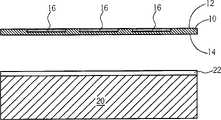
请参考图1至图5。图1至第图5为本发明的一优选实施例薄化晶片的方法示意图。如图1所示,首先,提供一晶片10,其包括一正面12与一背面14。接着进行一初步晶片薄化工艺,由晶片10的正面12薄化晶片10。于图1中,虚线所示为晶片10的初始厚度,通过初步晶片薄化工艺,晶片10的厚度可被缩减至一般工艺机器可固定传送的厚度,例如约100至150微米。另外,初步晶片薄化工艺可为一般现有研磨、化学机械研磨或化学蚀刻等工艺。Please refer to Figure 1 to Figure 5. 1 to 5 are schematic diagrams of a method for thinning a wafer according to a preferred embodiment of the present invention. As shown in FIG. 1 , firstly, a
如图2所示,接着提供一承载晶片20,并利用一接合媒介22将晶片10的下表面14固定于承载晶片20上。其中承载晶片20的尺寸与晶片10相近,藉此可适用于标准工艺机器固定传送,而承载晶片20的材料则可视需要采用半导体材料、玻璃、石英与陶瓷等。另外,接合媒介22用以接合晶片10与承载晶片20,且将于后续元件制作完成后去除,因此于材料的选用上需具有易去除的特性。于本实施例中,接合媒介22选用一热分离胶带,热分离胶带在温度高于其分离温度时会丧失其黏性,因此可轻易加以去除而不致导致晶片10受损。然而接合媒介22的材料并不限于热分离胶带,而可视需要选用紫外线胶带、光致抗蚀剂、腊与蓝膜等。As shown in FIG. 2 , a
如图3所示,接着进行一晶片薄化工艺,由晶片10的正面12缩减晶片10至所需的厚度,其中虚线所示为晶片10于晶片薄化工艺之前的厚度。晶片薄化工艺可为研磨工艺、化学机械研磨工艺、湿式蚀刻工艺或干式蚀刻工艺,且以干式蚀刻工艺优选。于本实施例中,晶片薄化工艺选用一等离子体蚀刻工艺,其理由在于等离子体蚀刻工艺为一干式工艺,因此不需于工艺完毕后另外进行清洗与干燥等工艺,减少了微粒污染与晶片10受损的风险。于晶片薄化工艺中,晶片10的厚度可进一步被缩减至100微米之下,甚至达到10微米左右,而由于晶片10通过接合媒介22固定于承载晶片20上,因此晶片10不致破裂,同时晶片10可利用承载晶片20进行固定与传送。As shown in FIG. 3 , a wafer thinning process is then performed to reduce the
如图4所示,由晶片10的正面12形成多个元件16,其中元件16可为半导体元件与微机电元件等,而制作元件16的方法并非本发明的重点,因此在此不另外赘述。如图5所示,接着去除接合媒介22,以分离晶片10与承载晶片20。如前所述,由本实施例中选用热分离胶带作为接合媒介22,因此仅需利用加热方式即可轻易分离晶片10与承载晶片20。若接合媒介22使用其它材料,例如紫外线胶带,则亦可利用照射紫外线方式加以去除。As shown in FIG. 4 , a plurality of
另外值得注意的是于上述实施例中,于晶片的正面形成元件后晶片即与承载晶片分离,然而本发明的应用并不局限于此。举例来说,于分离晶片与承载晶片之前可进一步整合后续切割工艺,若接合媒介选用可扩张的材料,例如蓝膜,则还可进一步整合扩片工艺。It is also worth noting that in the above embodiments, the chip is separated from the carrier chip after the components are formed on the front side of the chip, but the application of the present invention is not limited thereto. For example, the subsequent dicing process can be further integrated before separating the wafer and the carrier wafer. If the bonding medium is made of an expandable material, such as blue film, the wafer expansion process can be further integrated.
由上述可知,本发明薄化晶片的方法的主要特征在于先利用一接合媒介将晶片固定于一承载晶片上,接着再利用一晶片薄化工艺薄化晶片的厚度,在此状况下,晶片于进行晶片薄化工艺时具有良好的固定与支撑,可确保晶片不致破裂。相较于现有技术直接进行晶片薄化工艺的方法,本发明薄化晶片的方法可大幅提升晶片薄化工艺的极限,并有效避免应力集中与晶片翘曲(warp)等问题。As can be seen from the above, the main feature of the method for thinning a wafer of the present invention is to use a bonding medium to fix the wafer on a carrier wafer, and then utilize a wafer thinning process to thin the thickness of the wafer. It has good fixation and support during the wafer thinning process to ensure that the wafer will not break. Compared with the method of directly performing the wafer thinning process in the prior art, the wafer thinning method of the present invention can greatly increase the limit of the wafer thinning process, and effectively avoid problems such as stress concentration and wafer warp.
以上所述仅为本发明的优选实施例,凡依本发明权利要求所做的均等变化与修饰,皆应属本发明的涵盖范围。The above descriptions are only preferred embodiments of the present invention, and all equivalent changes and modifications made according to the claims of the present invention shall fall within the scope of the present invention.
Claims (18)
Priority Applications (1)
| Application Number | Priority Date | Filing Date | Title |
|---|---|---|---|
| CN 200510083342CN1897225A (en) | 2005-07-12 | 2005-07-12 | Methods of Thinning Wafers |
Applications Claiming Priority (1)
| Application Number | Priority Date | Filing Date | Title |
|---|---|---|---|
| CN 200510083342CN1897225A (en) | 2005-07-12 | 2005-07-12 | Methods of Thinning Wafers |
Publications (1)
| Publication Number | Publication Date |
|---|---|
| CN1897225Atrue CN1897225A (en) | 2007-01-17 |
Family
ID=37609690
Family Applications (1)
| Application Number | Title | Priority Date | Filing Date |
|---|---|---|---|
| CN 200510083342PendingCN1897225A (en) | 2005-07-12 | 2005-07-12 | Methods of Thinning Wafers |
Country Status (1)
| Country | Link |
|---|---|
| CN (1) | CN1897225A (en) |
Cited By (7)
| Publication number | Priority date | Publication date | Assignee | Title |
|---|---|---|---|---|
| CN102157426A (en)* | 2011-01-28 | 2011-08-17 | 上海宏力半导体制造有限公司 | Wafer support device and wafer processing process |
| CN102082070B (en)* | 2009-11-27 | 2012-07-11 | 北大方正集团有限公司 | A method of protecting metal layers during wafer thinning |
| CN102044472B (en)* | 2009-10-09 | 2013-03-06 | 中芯国际集成电路制造(上海)有限公司 | Method for reducing thickness of dielectric layer |
| CN105081893A (en)* | 2015-05-13 | 2015-11-25 | 北京通美晶体技术有限公司 | Ultrathin Ge single crystal substrate material and preparation method thereof |
| CN107877270A (en)* | 2017-11-10 | 2018-04-06 | 中国电子科技集团公司第四十研究所 | A kind of method for being uniformly thinned in dielectric substrate piece |
| CN112071762A (en)* | 2020-08-10 | 2020-12-11 | 长江存储科技有限责任公司 | Semiconductor device manufacturing method, semiconductor structure and semiconductor device |
| CN114334721A (en)* | 2021-12-15 | 2022-04-12 | 广州粤芯半导体技术有限公司 | Abnormal reworking method for thinning back of wafer |
- 2005
- 2005-07-12CNCN 200510083342patent/CN1897225A/enactivePending
Cited By (10)
| Publication number | Priority date | Publication date | Assignee | Title |
|---|---|---|---|---|
| CN102044472B (en)* | 2009-10-09 | 2013-03-06 | 中芯国际集成电路制造(上海)有限公司 | Method for reducing thickness of dielectric layer |
| CN102082070B (en)* | 2009-11-27 | 2012-07-11 | 北大方正集团有限公司 | A method of protecting metal layers during wafer thinning |
| CN102157426A (en)* | 2011-01-28 | 2011-08-17 | 上海宏力半导体制造有限公司 | Wafer support device and wafer processing process |
| CN102157426B (en)* | 2011-01-28 | 2015-10-07 | 上海华虹宏力半导体制造有限公司 | Wafer support and wafer processing process |
| CN105081893A (en)* | 2015-05-13 | 2015-11-25 | 北京通美晶体技术有限公司 | Ultrathin Ge single crystal substrate material and preparation method thereof |
| CN105081893B (en)* | 2015-05-13 | 2018-11-06 | 北京通美晶体技术有限公司 | A kind of ultra-thin Ge monocrystalline substrate materials and preparation method thereof |
| CN107877270A (en)* | 2017-11-10 | 2018-04-06 | 中国电子科技集团公司第四十研究所 | A kind of method for being uniformly thinned in dielectric substrate piece |
| CN107877270B (en)* | 2017-11-10 | 2020-03-17 | 中国电子科技集团公司第四十一研究所 | Method for uniformly thinning dielectric substrate in wafer |
| CN112071762A (en)* | 2020-08-10 | 2020-12-11 | 长江存储科技有限责任公司 | Semiconductor device manufacturing method, semiconductor structure and semiconductor device |
| CN114334721A (en)* | 2021-12-15 | 2022-04-12 | 广州粤芯半导体技术有限公司 | Abnormal reworking method for thinning back of wafer |
Similar Documents
| Publication | Publication Date | Title |
|---|---|---|
| TWI446420B (en) | Carrier separation method for semiconductor process | |
| JP5151104B2 (en) | Manufacturing method of electronic parts | |
| EP1497857B1 (en) | Method for handling semiconductor layers in such a way as to thin same | |
| US9595446B2 (en) | Methods of processing substrates | |
| CN100530593C (en) | Method of Dicing Wafers | |
| CN106663640B (en) | Method of providing electronic device and electronic device thereof | |
| EP1815509A2 (en) | Semiconductor wafer thinning | |
| JPH01312828A (en) | Manufacture of semiconductor | |
| JP2001326206A (en) | Method for thinning semiconductor wafer and thin semiconductor wafer | |
| TW201104732A (en) | Thin wafer structure and method | |
| CN104488066B (en) | Joint method in the atmosphere of the gas with negative joule thomson coefficient | |
| CN109972204B (en) | Ultra-thin ultra-flat wafer and method for manufacturing the same | |
| CN108242393B (en) | Method for manufacturing semiconductor device | |
| CN117016057A (en) | Method for transferring layers of a heterostructure | |
| JP2005150434A (en) | Manufacturing method of semiconductor wafer | |
| JP4271409B2 (en) | Processing method for brittle materials | |
| CN1897225A (en) | Methods of Thinning Wafers | |
| JPH0917984A (en) | Method for manufacturing bonded SOI substrate | |
| TWI236058B (en) | Method of performing double side processes upon a wafer | |
| CN112201566A (en) | Wafer thinning method and device and wafer unloading clamp | |
| JP7186921B2 (en) | Semiconductor device manufacturing method | |
| CN101075559A (en) | Methods of Thinning Wafers | |
| TWI310583B (en) | Method of thinning a wafer | |
| CN102479674B (en) | Wafer manufacturing method | |
| CN111384204A (en) | Back processing technology of back-illuminated photoelectric device |
Legal Events
| Date | Code | Title | Description |
|---|---|---|---|
| C06 | Publication | ||
| PB01 | Publication | ||
| C10 | Entry into substantive examination | ||
| SE01 | Entry into force of request for substantive examination | ||
| C02 | Deemed withdrawal of patent application after publication (patent law 2001) | ||
| WD01 | Invention patent application deemed withdrawn after publication |