CN1892765A - Display device and driving method - Google Patents
Display device and driving methodDownload PDFInfo
- Publication number
- CN1892765A CN1892765ACNA2006100871760ACN200610087176ACN1892765ACN 1892765 ACN1892765 ACN 1892765ACN A2006100871760 ACNA2006100871760 ACN A2006100871760ACN 200610087176 ACN200610087176 ACN 200610087176ACN 1892765 ACN1892765 ACN 1892765A
- Authority
- CN
- China
- Prior art keywords
- thin film
- film transistor
- switching element
- pixel
- gate
- Prior art date
- Legal status (The legal status is an assumption and is not a legal conclusion. Google has not performed a legal analysis and makes no representation as to the accuracy of the status listed.)
- Granted
Links
Images
Classifications
- G—PHYSICS
- G09—EDUCATION; CRYPTOGRAPHY; DISPLAY; ADVERTISING; SEALS
- G09G—ARRANGEMENTS OR CIRCUITS FOR CONTROL OF INDICATING DEVICES USING STATIC MEANS TO PRESENT VARIABLE INFORMATION
- G09G3/00—Control arrangements or circuits, of interest only in connection with visual indicators other than cathode-ray tubes
- G09G3/20—Control arrangements or circuits, of interest only in connection with visual indicators other than cathode-ray tubes for presentation of an assembly of a number of characters, e.g. a page, by composing the assembly by combination of individual elements arranged in a matrix no fixed position being assigned to or needed to be assigned to the individual characters or partial characters
- G09G3/22—Control arrangements or circuits, of interest only in connection with visual indicators other than cathode-ray tubes for presentation of an assembly of a number of characters, e.g. a page, by composing the assembly by combination of individual elements arranged in a matrix no fixed position being assigned to or needed to be assigned to the individual characters or partial characters using controlled light sources
- G09G3/30—Control arrangements or circuits, of interest only in connection with visual indicators other than cathode-ray tubes for presentation of an assembly of a number of characters, e.g. a page, by composing the assembly by combination of individual elements arranged in a matrix no fixed position being assigned to or needed to be assigned to the individual characters or partial characters using controlled light sources using electroluminescent panels
- G09G3/32—Control arrangements or circuits, of interest only in connection with visual indicators other than cathode-ray tubes for presentation of an assembly of a number of characters, e.g. a page, by composing the assembly by combination of individual elements arranged in a matrix no fixed position being assigned to or needed to be assigned to the individual characters or partial characters using controlled light sources using electroluminescent panels semiconductive, e.g. using light-emitting diodes [LED]
- G09G3/3208—Control arrangements or circuits, of interest only in connection with visual indicators other than cathode-ray tubes for presentation of an assembly of a number of characters, e.g. a page, by composing the assembly by combination of individual elements arranged in a matrix no fixed position being assigned to or needed to be assigned to the individual characters or partial characters using controlled light sources using electroluminescent panels semiconductive, e.g. using light-emitting diodes [LED] organic, e.g. using organic light-emitting diodes [OLED]
- G09G3/3225—Control arrangements or circuits, of interest only in connection with visual indicators other than cathode-ray tubes for presentation of an assembly of a number of characters, e.g. a page, by composing the assembly by combination of individual elements arranged in a matrix no fixed position being assigned to or needed to be assigned to the individual characters or partial characters using controlled light sources using electroluminescent panels semiconductive, e.g. using light-emitting diodes [LED] organic, e.g. using organic light-emitting diodes [OLED] using an active matrix
- G—PHYSICS
- G09—EDUCATION; CRYPTOGRAPHY; DISPLAY; ADVERTISING; SEALS
- G09G—ARRANGEMENTS OR CIRCUITS FOR CONTROL OF INDICATING DEVICES USING STATIC MEANS TO PRESENT VARIABLE INFORMATION
- G09G3/00—Control arrangements or circuits, of interest only in connection with visual indicators other than cathode-ray tubes
- G09G3/20—Control arrangements or circuits, of interest only in connection with visual indicators other than cathode-ray tubes for presentation of an assembly of a number of characters, e.g. a page, by composing the assembly by combination of individual elements arranged in a matrix no fixed position being assigned to or needed to be assigned to the individual characters or partial characters
- G09G3/22—Control arrangements or circuits, of interest only in connection with visual indicators other than cathode-ray tubes for presentation of an assembly of a number of characters, e.g. a page, by composing the assembly by combination of individual elements arranged in a matrix no fixed position being assigned to or needed to be assigned to the individual characters or partial characters using controlled light sources
- G09G3/30—Control arrangements or circuits, of interest only in connection with visual indicators other than cathode-ray tubes for presentation of an assembly of a number of characters, e.g. a page, by composing the assembly by combination of individual elements arranged in a matrix no fixed position being assigned to or needed to be assigned to the individual characters or partial characters using controlled light sources using electroluminescent panels
- G09G3/32—Control arrangements or circuits, of interest only in connection with visual indicators other than cathode-ray tubes for presentation of an assembly of a number of characters, e.g. a page, by composing the assembly by combination of individual elements arranged in a matrix no fixed position being assigned to or needed to be assigned to the individual characters or partial characters using controlled light sources using electroluminescent panels semiconductive, e.g. using light-emitting diodes [LED]
- G09G3/3208—Control arrangements or circuits, of interest only in connection with visual indicators other than cathode-ray tubes for presentation of an assembly of a number of characters, e.g. a page, by composing the assembly by combination of individual elements arranged in a matrix no fixed position being assigned to or needed to be assigned to the individual characters or partial characters using controlled light sources using electroluminescent panels semiconductive, e.g. using light-emitting diodes [LED] organic, e.g. using organic light-emitting diodes [OLED]
- G09G3/3225—Control arrangements or circuits, of interest only in connection with visual indicators other than cathode-ray tubes for presentation of an assembly of a number of characters, e.g. a page, by composing the assembly by combination of individual elements arranged in a matrix no fixed position being assigned to or needed to be assigned to the individual characters or partial characters using controlled light sources using electroluminescent panels semiconductive, e.g. using light-emitting diodes [LED] organic, e.g. using organic light-emitting diodes [OLED] using an active matrix
- G09G3/3233—Control arrangements or circuits, of interest only in connection with visual indicators other than cathode-ray tubes for presentation of an assembly of a number of characters, e.g. a page, by composing the assembly by combination of individual elements arranged in a matrix no fixed position being assigned to or needed to be assigned to the individual characters or partial characters using controlled light sources using electroluminescent panels semiconductive, e.g. using light-emitting diodes [LED] organic, e.g. using organic light-emitting diodes [OLED] using an active matrix with pixel circuitry controlling the current through the light-emitting element
- G09G3/3241—Control arrangements or circuits, of interest only in connection with visual indicators other than cathode-ray tubes for presentation of an assembly of a number of characters, e.g. a page, by composing the assembly by combination of individual elements arranged in a matrix no fixed position being assigned to or needed to be assigned to the individual characters or partial characters using controlled light sources using electroluminescent panels semiconductive, e.g. using light-emitting diodes [LED] organic, e.g. using organic light-emitting diodes [OLED] using an active matrix with pixel circuitry controlling the current through the light-emitting element the current through the light-emitting element being set using a data current provided by the data driver, e.g. by using a two-transistor current mirror
- G09G3/325—Control arrangements or circuits, of interest only in connection with visual indicators other than cathode-ray tubes for presentation of an assembly of a number of characters, e.g. a page, by composing the assembly by combination of individual elements arranged in a matrix no fixed position being assigned to or needed to be assigned to the individual characters or partial characters using controlled light sources using electroluminescent panels semiconductive, e.g. using light-emitting diodes [LED] organic, e.g. using organic light-emitting diodes [OLED] using an active matrix with pixel circuitry controlling the current through the light-emitting element the current through the light-emitting element being set using a data current provided by the data driver, e.g. by using a two-transistor current mirror the data current flowing through the driving transistor during a setting phase, e.g. by using a switch for connecting the driving transistor to the data driver
- G—PHYSICS
- G09—EDUCATION; CRYPTOGRAPHY; DISPLAY; ADVERTISING; SEALS
- G09G—ARRANGEMENTS OR CIRCUITS FOR CONTROL OF INDICATING DEVICES USING STATIC MEANS TO PRESENT VARIABLE INFORMATION
- G09G2300/00—Aspects of the constitution of display devices
- G09G2300/04—Structural and physical details of display devices
- G09G2300/0421—Structural details of the set of electrodes
- G09G2300/0426—Layout of electrodes and connections
- G—PHYSICS
- G09—EDUCATION; CRYPTOGRAPHY; DISPLAY; ADVERTISING; SEALS
- G09G—ARRANGEMENTS OR CIRCUITS FOR CONTROL OF INDICATING DEVICES USING STATIC MEANS TO PRESENT VARIABLE INFORMATION
- G09G2300/00—Aspects of the constitution of display devices
- G09G2300/08—Active matrix structure, i.e. with use of active elements, inclusive of non-linear two terminal elements, in the pixels together with light emitting or modulating elements
- G09G2300/0809—Several active elements per pixel in active matrix panels
- G09G2300/0814—Several active elements per pixel in active matrix panels used for selection purposes, e.g. logical AND for partial update
Landscapes
- Engineering & Computer Science (AREA)
- Physics & Mathematics (AREA)
- Computer Hardware Design (AREA)
- General Physics & Mathematics (AREA)
- Theoretical Computer Science (AREA)
- Electroluminescent Light Sources (AREA)
- Control Of El Displays (AREA)
- Control Of Indicators Other Than Cathode Ray Tubes (AREA)
Abstract
Translated fromChinese
Description
Translated fromChinese本申请要求于2005年6月30日提交的在先韩国专利申请No.2005-057485的权益,在此将其全部内容结合进来作为参考。This application claims the benefit of prior Korean Patent Application No. 2005-057485 filed on Jun. 30, 2005, the entire contents of which are hereby incorporated by reference.
技术领域technical field
本申请涉及一种显示装置,特别是涉及一种有机电致发光显示(OELD)装置及一种驱动OELD装置的方法。The present application relates to a display device, in particular to an organic electroluminescence display (OELD) device and a method for driving the OELD device.
背景技术Background technique
显示装置已经采用了阴极射线管(CRT)来显示图像。但是,当前正在开发用于替代CRT的各种类型的平板显示器,诸如液晶显示(LCD)装置,等离子体显示板(PDP)装置,场发射显示(FED)装置以及电致发光显示(ELD)装置。在这些各种类型的平板显示器中,LCD装置具有外形薄和功耗低的优点,但是由于其为非发光显示装置而具有使用背光单元的缺点。然而,由于有机电致发光显示(OELD)装置为自发光显示装置,其在低电压下工作,并具有薄的外形。另外,OELD装置具有响应时间快,亮度高和视角宽的优点。Display devices have employed cathode ray tubes (CRTs) to display images. However, various types of flat panel displays such as liquid crystal display (LCD) devices, plasma display panel (PDP) devices, field emission display (FED) devices, and electroluminescence display (ELD) devices are currently being developed to replace CRTs. . Among these various types of flat panel displays, the LCD device has advantages of a thin profile and low power consumption, but has a disadvantage of using a backlight unit because it is a non-emissive display device. However, since an organic electroluminescent display (OELD) device is a self-luminous display device, it operates at a low voltage and has a thin profile. In addition, the OELD device has the advantages of fast response time, high brightness and wide viewing angle.
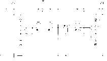
如图1所示,现有技术的OELD装置的像素连接到栅线S,数据线D和电源线VDD。该像素包括开关薄膜晶体管N1,驱动薄膜晶体管N2,电容器C和有机发光二极管OLED。As shown in FIG. 1, the pixels of the prior art OELD device are connected to a gate line S, a data line D and a power line VDD. The pixel includes a switching thin film transistor N1, a driving thin film transistor N2, a capacitor C and an organic light emitting diode OLED.
开关薄膜晶体管N1的栅极连接到栅线S,开关薄膜晶体管N1的源极连接到数据线D。电容器C的一个电极连接到开关薄膜晶体管N1的漏极,而电容器C的另一个电极连接到接地端子(GND)。驱动薄膜晶体管N2的漏极连接到有机发光二极管OLED的阴极,驱动薄膜晶体管N2的栅极连接到开关薄膜晶体管N1的漏极,并且驱动薄膜晶体管N2的源极连接到接地端子(GND)。The gate of the switching thin film transistor N1 is connected to the gate line S, and the source of the switching thin film transistor N1 is connected to the data line D. One electrode of the capacitor C is connected to the drain of the switching thin film transistor N1, and the other electrode of the capacitor C is connected to the ground terminal (GND). The drain of the driving thin film transistor N2 is connected to the cathode of the organic light emitting diode OLED, the gate of the driving thin film transistor N2 is connected to the drain of the switching thin film transistor N1, and the source of the driving thin film transistor N2 is connected to the ground terminal (GND).
图2是施加到图1的像素上的栅信号、数据信号和电源信号的波形图。具有高电平或低电平即VGH或VGL的栅信号通过栅线S施加到开关薄膜晶体管N1。当施加高电平VGH时,开关薄膜晶体管N1导通。当开关薄膜晶体管N1导通时,数据信号存储到电容器C并且驱动薄膜晶体管N2导通。因此,在驱动薄膜晶体管N2上有电流流动,且有机发光二极管OLED发光。存储的数据信号决定了在驱动薄膜晶体管N2上流动的电流的大小,并且该电流的大小决定了有机发光二极管OLED的光强。FIG. 2 is a waveform diagram of a gate signal, a data signal, and a power signal applied to the pixel of FIG. 1. Referring to FIG. A gate signal having a high level or a low level, ie, VGH or VGL, is applied to the switching thin film transistor N1 through the gate line S. When the high level VGH is applied, the switching thin film transistor N1 is turned on. When the switching thin film transistor N1 is turned on, the data signal is stored in the capacitor C and the driving thin film transistor N2 is turned on. Therefore, a current flows in the driving thin film transistor N2, and the organic light emitting diode OLED emits light. The stored data signal determines the magnitude of the current flowing on the driving thin film transistor N2, and the magnitude of the current determines the light intensity of the organic light emitting diode OLED.
当将现有技术的OELD装置用作高分辨率显示装置时,所需要的信号线和驱动IC的数量增加。当将OELD装置用作高分辨率和小尺寸的显示装置时,所需要的元件的安装空间可能不够。When the related art OELD device is used as a high-resolution display device, the number of required signal lines and driving ICs increases. When an OELD device is used as a high-resolution and small-sized display device, the installation space of required components may be insufficient.
发明内容Contents of the invention
本发明公开了一种显示装置,其包括:数据线;第一和第二栅线;包括第一开关元件的第一像素,该第一开关元件连接到该数据线和该第一栅线;以及包括第二开关元件的第二像素,该第二开关元件连接到该数据线和该第一和第二栅线。The invention discloses a display device, which comprises: a data line; a first and a second gate line; a first pixel including a first switch element connected to the data line and the first gate line; and a second pixel including a second switching element connected to the data line and the first and second gate lines.
在另一方面,一种驱动显示装置的方法包括:在水平时间间隔的第一和第二时间内导通第一像素的第一开关元件,并在该第一时间内导通第二像素的第二开关元件;以及,分别在该第一和第二时间内将第一和第二数据信号提供给连接到该第一和第二像素的数据线。In another aspect, a method of driving a display device includes: turning on a first switching element of a first pixel during first and second times of a horizontal time interval, and turning on a switching element of a second pixel during the first time. a second switching element; and, supplying first and second data signals to data lines connected to the first and second pixels for the first and second times, respectively.
在又一方面,一种驱动显示装置的方法包括:分别在水平时间间隔的第一和第二时间内提供第一和第二数据信号;并在该第一和第二时间内分别将该第一和第二数据信号存储到第一像素,并且在该第一时间内将该第一数据信号存储到第二像素。In yet another aspect, a method of driving a display device includes: providing first and second data signals during first and second times of a horizontal time interval, respectively; One and second data signals are stored to the first pixel, and the first data signal is stored to the second pixel for the first time.
附图说明Description of drawings
图1是按照现有技术的OELD装置的电路图;FIG. 1 is a circuit diagram of an OELD device according to the prior art;
图2是施加到图1的像素上的栅信号、数据信号和电源信号的波形图;Fig. 2 is a waveform diagram of a gate signal, a data signal and a power signal applied to the pixel of Fig. 1;
图3是按照本发明一示范性实施例的OELD装置的电路图;3 is a circuit diagram of an OELD device according to an exemplary embodiment of the present invention;
图4是描绘驱动按照该示范性实施例的OELD装置的方法的电路图;4 is a circuit diagram depicting a method of driving an OELD device according to this exemplary embodiment;
图5是用于驱动图4的OELD装置的栅信号的波形图;5 is a waveform diagram of a gate signal for driving the OELD device of FIG. 4;
图6是按照本发明另一示范性实施例的OELD装置的电路图;以及6 is a circuit diagram of an OELD device according to another exemplary embodiment of the present invention; and
图7是用于驱动图6的OELD装置的栅信号的波形图。FIG. 7 is a waveform diagram of a gate signal for driving the OELD device of FIG. 6 .
具体实施方式Detailed ways
参考附图可以更好地理解示范性的实施例,但是这些实施例并不用于作为限制。在相同或不同的图中编号相同的元件起等效的作用。当描述与一个实施例相关的具体特征、结构或特性时,应当理解,无论此处是否明确地声明,本领域技术人员都可以在其他实施例中实现这些特征、结构或特性。Exemplary embodiments may be better understood with reference to the accompanying drawings, which are not intended to be limiting. Elements numbered the same in the same or different figures serve equivalent functions. When a specific feature, structure or characteristic is described in connection with one embodiment, it is to be understood that those skilled in the art can implement that feature, structure or characteristic in other embodiments whether or not expressly stated herein.
图3示出了在第一实例中的有机发光二极管(OLED)装置的局部电路图。两个像素OP和EP按列设置在数据线D的相对侧,并且每个均连接到相同的数据线D。在数据线D左侧的像素OP称作奇像素OP,而在数据线D右侧的像素EP称作偶像素。由此,奇像素和偶像素即OP和EP共享相同的数据线D,并且对奇像素和偶像素OP和EP施加相同的数据信号。通过电源线VDD为奇像素和偶像素OP和EP提供电源。Fig. 3 shows a partial circuit diagram of an organic light emitting diode (OLED) device in a first example. The two pixels OP and EP are arranged on opposite sides of the data line D in columns, and are each connected to the same data line D. Referring to FIG. The pixels OP on the left side of the data line D are called odd pixels OP, and the pixels EP on the right side of the data line D are called even pixels. Thus, the odd and even pixels, ie, OP and EP, share the same data line D, and the same data signal is applied to the odd and even pixels OP and EP. Odd and even pixels OP and EP are powered through the power line VDD.
尽管奇像素和偶像素OP和EP连接到相同的数据线D,但是奇像素和偶像素OP和EP连接到不同的栅线S(n)和S(n+1)。奇像素OP连接到第n条栅线S(n),而偶像素EP同时连接到第(n+1)条和第n条栅线S(n)和S(n+1)。Although the odd and even pixels OP and EP are connected to the same data line D, the odd and even pixels OP and EP are connected to different gate lines S(n) and S(n+1). The odd pixel OP is connected to the nth gate line S(n), and the even pixel EP is connected to both the (n+1)th and nth gate lines S(n) and S(n+1).
由此,奇像素OP包括奇开关元件,奇驱动元件,奇电容器C_O和奇有机发光二极管OLED_O。奇开关元件包括串联的第一开关薄膜晶体管SW_O1和第二奇开关薄膜晶体管SW_O2。第一和第二奇开关薄膜晶体管SW_O1和SW_O2连接到第n条栅线S(n)。第一奇开关薄膜晶体管SW_O1也连接到数据线D。Thus, the odd pixel OP includes an odd switching element, an odd driving element, an odd capacitor C_O, and an odd organic light emitting diode OLED_O. The odd switching element includes a first switching thin film transistor SW_O1 and a second odd switching thin film transistor SW_O2 connected in series. The first and second odd switching thin film transistors SW_O1 and SW_O2 are connected to the nth gate line S(n). The first odd switching thin film transistor SW_O1 is also connected to the data line D.
奇驱动元件包括奇驱动薄膜晶体管D_O。该奇驱动薄膜晶体管D_O的栅极连接到第二奇开关薄膜晶体管SW_O2的漏极。The odd driving element includes an odd driving thin film transistor D_O. The gate of the odd driving TFT D_O is connected to the drain of the second odd switching TFT SW_O2.
奇电容器C_O连接到奇驱动薄膜晶体管D_O的栅极和源极。奇发光二极管OLED_O连接到电源线VDD和奇驱动薄膜晶体管D_O的漏极。The odd capacitor C_O is connected to the gate and source of the odd driving thin film transistor D_O. The odd light emitting diodes OLED_O are connected to the power line VDD and the drains of the odd driving thin film transistors D_O.
由于第一和第二奇开关薄膜晶体管SW_O1和SW_O2连接到相同的第n条栅线S(n),因此奇开关元件根据施加到第n条栅线S(n)上的栅信号是ON或OFF(高电平或低电平)而导通或关断。Since the first and second odd switching thin film transistors SW_O1 and SW_O2 are connected to the same nth gate line S(n), the odd switching elements are ON or ON according to the gate signal applied to the nth gate line S(n). OFF (high level or low level) and turn on or off.
当奇开关元件导通时,数据线D上的数据信号通过奇开关元件。然后,该数据信号被存储到奇电容器C_O上并被施加到该奇驱动元件。当对奇驱动薄膜晶体管D_O提供该数据信号时,奇驱动薄膜晶体管D_O导通。当奇驱动薄膜晶体管D_O导通时,电流在奇驱动薄膜晶体管D_O上流动,并且奇有机发光二极管OLED_O发光。存储在奇电容器C_O上的该数据信号决定了在奇驱动薄膜晶体管D_O上流动的电流的大小,并且该电流的大小决定了从奇有机发光二极管OLED_O发射的光强。When the odd switch element is turned on, the data signal on the data line D passes through the odd switch element. Then, the data signal is stored on the odd capacitor C_O and applied to the odd drive element. When the data signal is supplied to the odd driving thin film transistor D_O, the odd driving thin film transistor D_O is turned on. When the odd driving thin film transistor D_O is turned on, current flows on the odd driving thin film transistor D_O, and the odd organic light emitting diode OLED_O emits light. The data signal stored in the odd capacitor C_O determines the magnitude of the current flowing in the odd driving thin film transistor D_O, and the magnitude of the current determines the light intensity emitted from the odd organic light emitting diode OLED_O.
偶像素EP包括偶开关元件,偶驱动元件,偶电容器C_E和偶有机发光二极管OLED_E。该偶开关元件包括串联的第一和第二偶开关薄膜晶体管SW_E1和SW_E2。该第一和第二偶开关薄膜晶体管SW_E1和SW_E2分别连接到第(n+1)条和第n条栅线S(n+1)和S(n)。该第一偶开关薄膜晶体管SW_E1连接到数据线D。第一和第二偶开关薄膜晶体管SW_E1和SW_E2可以分别连接到第n条和第(n+1)条栅线S(n)和S(n+1)。The even pixel EP includes an even switching element, an even driving element, an even capacitor C_E, and an even organic light emitting diode OLED_E. The even switching element includes first and second even switching thin film transistors SW_E1 and SW_E2 connected in series. The first and second even switching thin film transistors SW_E1 and SW_E2 are respectively connected to the (n+1)th and nth gate lines S(n+1) and S(n). The first even switching TFT SW_E1 is connected to the data line D. As shown in FIG. The first and second even switching thin film transistors SW_E1 and SW_E2 may be connected to the nth and (n+1)th gate lines S(n) and S(n+1), respectively.
偶驱动元件包括偶驱动薄膜晶体管D_E。偶驱动薄膜晶体管D_E的栅极连接到第二偶开关薄膜晶体管SW_E2的漏极。The even driving element includes an even driving thin film transistor D_E. The gate of the even driving thin film transistor D_E is connected to the drain of the second even switching thin film transistor SW_E2.
偶电容器C_E连接到偶驱动薄膜晶体管D_E的栅极和源极。偶有机发光二极管OLED_E连接到电源线VDD和偶驱动薄膜晶体管D_E的漏极。The even capacitor C_E is connected to the gate and source of the even driving thin film transistor D_E. The even organic light emitting diode OLED_E is connected to the power supply line VDD and the drain of the even driving thin film transistor D_E.
当同时在第(n+1)条和第n条栅线S(n+1)和S(n)上施加ON栅信号时,偶开关元件导通,否则,偶开关元件关断。这是由于第一和第二偶开关薄膜晶体管SW_E1和SW_E2连接到不同的栅线S(n+1)和S(n)。When the ON gate signal is applied to the (n+1)th and nth gate lines S(n+1) and S(n) at the same time, the even switching element is turned on, otherwise, the even switching element is turned off. This is because the first and second even switching thin film transistors SW_E1 and SW_E2 are connected to different gate lines S(n+1) and S(n).
当偶开关元件导通时,数据线D上的数据信号通过偶开关元件。然后,该数据信号被存储到偶电容器C_E上并被施加到该偶驱动元件。当对偶驱动薄膜晶体管D_E提供该数据信号时,偶驱动薄膜晶体管D_E导通。当偶驱动薄膜晶体管D_E导通时,电流在偶驱动薄膜晶体管D_E上流动并且偶有机发光二极管OLED_E发光。存储在偶电容器C_E上的该数据信号决定了在偶驱动薄膜晶体管D_E上流动的电流的大小,并且该电流的大小决定了从偶有机发光二极管OLED_E发射的光强。When the even switching element is turned on, the data signal on the data line D passes through the even switching element. Then, the data signal is stored on the even capacitor C_E and applied to the even drive element. When the pair driving TFT D_E provides the data signal, the even driving TFT D_E is turned on. When the even driving thin film transistor D_E is turned on, current flows on the even driving thin film transistor D_E and the even organic light emitting diode OLED_E emits light. The data signal stored in the even capacitor C_E determines the magnitude of the current flowing in the even driving thin film transistor D_E, and the magnitude of the current determines the light intensity emitted from the even organic light emitting diode OLED_E.
图4是描绘了驱动OELD装置的方法的电路图,图5是用于驱动图4中的OELD装置的栅信号的波形图。FIG. 4 is a circuit diagram depicting a method of driving an OELD device, and FIG. 5 is a waveform diagram of a gate signal for driving the OELD device in FIG. 4 .
在图4中,左边两个像素(P1,P3)对应于图3中的奇像素,右边两个像素(P2,P4)对应于图3中的偶像素。在每个像素内对应的元件具有相同的附图标记。第一至第四像素P1至P4中的每一个包括第一和第二开关薄膜晶体管SW1和SW2、驱动薄膜晶体管DR、电容器C和有机发光二极管OLED。In FIG. 4 , the left two pixels ( P1 , P3 ) correspond to odd pixels in FIG. 3 , and the right two pixels ( P2 , P4 ) correspond to even pixels in FIG. 3 . Corresponding elements within each pixel have the same reference numerals. Each of the first to fourth pixels P1 to P4 includes first and second switching thin film transistors SW1 and SW2, a driving thin film transistor DR, a capacitor C, and an organic light emitting diode OLED.
将具有ON和OFF(高和低)电平的栅信号依次提供给第n条至第(n+2)条栅线S(n)至S(n+2)。以一个水平时间间隔H的延迟,栅信号被依次提供到第n条至第(n+2)条栅线S(n)至S(n+2)。水平时间间隔H是将数据信号提供到一个行线内的像素上的时间。栅信号具有两个ON电平。也就是说,栅信号在水平时间间隔的第一半(H/2)时间里持续具有第一ON电平,在水平时间间隔的第二半时间里持续具有OFF电平,以及在下一水平时间间隔里持续具有第二ON电平。因此,相邻的栅线在半个水平时间间隔(H/2)的时间里同时持续具有ON电平。在水平时间间隔H的第二半可以具有第一ON电平,而水平时间间隔H的第一半可以具有OFF电平。Gate signals having ON and OFF (high and low) levels are sequentially supplied to the nth to (n+2)th gate lines S(n) to S(n+2). With a delay of one horizontal time interval H, the gate signal is sequentially supplied to the nth to (n+2)th gate lines S(n) to S(n+2). The horizontal time interval H is the time during which data signals are supplied to pixels within one row line. The gate signal has two ON levels. That is, the gate signal continues to have the first ON level for the first half (H/2) of the horizontal time interval, continues to have the OFF level for the second half of the horizontal time interval, and The interval has the second ON level continuously. Therefore, the adjacent gate lines simultaneously continue to have ON levels for half a horizontal time interval (H/2). The second half of the horizontal time interval H may have the first ON level, and the first half of the horizontal time interval H may have the OFF level.
在第一个水平时间间隔H_1的第一半,为第n条和第(n+1)条栅线S(n)和S(n+1)提供ON栅信号,并将第一数据信号提供到数据线D。第一和第二像素P1和P2的第一和第二开关薄膜晶体管SW_1和SW_2导通。将该第一数据信号同时施加到该第一和第二像素P1和P2,并存储到该第一和第二像素P1和P2的电容器C内。In the first half of the first horizontal time interval H_1, the ON gate signal is provided for the nth and (n+1)th gate lines S(n) and S(n+1), and the first data signal is provided to data line D. The first and second switching thin film transistors SW_1 and SW_2 of the first and second pixels P1 and P2 are turned on. The first data signal is simultaneously applied to the first and second pixels P1 and P2, and stored in the capacitors C of the first and second pixels P1 and P2.
在该第一水平时间间隔H_1的第二半内,仍然对该第n条栅线S(n)提供ON栅信号,而对该第(n+1)条栅线S(n+1)提供OFF栅信号,并将第二数据信号提供到数据线D。第二像素P2的第一开关薄膜晶体管SW_1关断,并且该第二像素P2存储该第一数据信号。该第一像素P1的第一和第二开关薄膜晶体管SW_1和SW_2仍然导通,并且第一像素P1存储该第二数据信号而不是该第一数据信号。In the second half of the first horizontal time interval H_1, the ON gate signal is still provided to the nth gate line S(n), while the (n+1)th gate line S(n+1) is provided with The gate signal is OFF, and the second data signal is supplied to the data line D. The first switching thin film transistor SW_1 of the second pixel P2 is turned off, and the second pixel P2 stores the first data signal. The first and second switching thin film transistors SW_1 and SW_2 of the first pixel P1 are still turned on, and the first pixel P1 stores the second data signal instead of the first data signal.
如上所解释的,第n条栅线S(n)在第一水平时间间隔H_1内具有ON栅信号,并且第(n+1)条栅线S(n+1)在第一水平时间间隔H_1的第一半内持续具有ON栅信号。在第一水平时间间隔H_1的第一半内持续提供第一数据信号,而在第一水平时间间隔H_1的第二半内持续提供第二数据信号。第一像素P1的开关元件在第一水平时间间隔内持续导通,并因此该第一像素P1在该第一半的时间内存储该第一数据信号,并且最终取代该第一数据信号在该第二半的时间内存储该第二数据信号。第二像素P2的开关元件在该第一半的时间内持续导通,及在该第二半时间内关断,并由此第二像素P2存储该第一数据信号。As explained above, the nth gate line S(n) has an ON gate signal in the first horizontal time interval H_1, and the (n+1)th gate line S(n+1) has an ON gate signal in the first horizontal time interval H_1 The first half of the continuation has an ON gate signal. The first data signal is continuously provided during the first half of the first horizontal time interval H_1, and the second data signal is continuously provided during the second half of the first horizontal time interval H_1. The switching element of the first pixel P1 is continuously turned on in the first horizontal time interval, and thus the first pixel P1 stores the first data signal in the first half of the time, and finally replaces the first data signal in the first half of the time. The second data signal is stored for the second half of the time. The switching element of the second pixel P2 is continuously turned on during the first half of the time, and turned off during the second half of the time, so that the second pixel P2 stores the first data signal.
在第二水平时间间隔H_2的第一半时间内,对第(n+1)条和第(n+2)条栅线S(n+1)和S(n+2)提供ON栅信号,并将该第三数据信号提供到该数据线D。该第三和第四像素P3和P4的第一和第二开关薄膜晶体管SW_1和SW_2导通。对该第三和第四像素P3和P4都施加第三数据信号,并将其存储到该第三和第四像素P3和P4的电容器C内。第三像素P3先前在第一水平时间间隔H_1的第一半时间内存储该第一数据信号,但在该第二水平时间间隔H_2的该第一半时间内,该第三像素P3存储该第三数据信号,而不是该第一数据信号。During the first half of the second horizontal time interval H_2, an ON gate signal is provided to the (n+1)th and (n+2)th gate lines S(n+1) and S(n+2), And provide the third data signal to the data line D. The first and second switching thin film transistors SW_1 and SW_2 of the third and fourth pixels P3 and P4 are turned on. The third data signal is applied to both the third and fourth pixels P3 and P4 and stored in the capacitor C of the third and fourth pixels P3 and P4. The third pixel P3 previously stored the first data signal during the first half of the first horizontal time interval H_1, but during the first half of the second horizontal time interval H_2, the third pixel P3 stored the first data signal three data signals instead of the first data signal.
在第二水平时间间隔H_2的第二半时间内,仍然对第(n+1)条栅线S(n+1)提供ON栅信号,而对该第(n+2)条栅线S(n+2)提供OFF栅信号,并且将第四数据信号提供到数据线D。第四像素P4的第一开关薄膜晶体管SW_1关断,并且第四像素P4存储该第三数据信号。第三像素P3的该第一和第二薄膜晶体管SW_1和SW_2仍然导通,并且该第三像素P3存储该第四数据信号,而不是该第三数据信号。In the second half time of the second horizontal time interval H_2, the ON gate signal is still provided to the (n+1)th gate line S(n+1), while the (n+2)th gate line S( n+2) supplies an OFF gate signal, and supplies a fourth data signal to the data line D. FIG. The first switching thin film transistor SW_1 of the fourth pixel P4 is turned off, and the fourth pixel P4 stores the third data signal. The first and second thin film transistors SW_1 and SW_2 of the third pixel P3 are still turned on, and the third pixel P3 stores the fourth data signal instead of the third data signal.
如上所解释的,第(n+1)条栅线S(n+1)具有持续第二水平时间间隔H_2的ON栅信号,而第(n+2)条栅线S(n+2)具有持续该第二水平时间间隔H_2的第一半的ON栅信号。在第二水平时间间隔H_2的第一半时间内持续提供第三数据信号,并在第二水平时间间隔H_2的第二半时间内持续提供第四数据信号。第三像素P3的开关元件在第一水平时间间隔内持续导通,并由此该第三像素P3在该第一半时间内持续存储该第三数据信号,并且取代该第三数据信号在该第二半时间内持续存储该第四数据信号。第四像素P4的开关元件在该第一半时间内持续导通并在该第二半内时间关断,并由此第四像素P4存储该第三数据信号。As explained above, the (n+1)th gate line S(n+1) has the ON gate signal for the second horizontal time interval H_2, and the (n+2)th gate line S(n+2) has The ON gate signal lasts for the first half of the second horizontal time interval H_2. The third data signal is continuously provided during the first half of the second horizontal time interval H_2, and the fourth data signal is continuously provided during the second half of the second horizontal time interval H_2. The switching element of the third pixel P3 is continuously turned on during the first horizontal time interval, and thus the third pixel P3 continuously stores the third data signal in the first half time, and replaces the third data signal in the first half time. The fourth data signal is continuously stored for the second half time. The switching element of the fourth pixel P4 is continuously turned on during the first half of the time and turned off during the second half of the time, and thus the fourth pixel P4 stores the third data signal.
结果,该第一至第四像素P1至P4具有所需要的数据信号。该第一至第四像素P1至P4的驱动薄膜晶体管根据存储的数据信号被导通,并且第一至第四像素P1至P4的发光二极管OLED相应于该存储的数据信号发光。As a result, the first to fourth pixels P1 to P4 have required data signals. The driving thin film transistors of the first to fourth pixels P1 to P4 are turned on according to the stored data signal, and the light emitting diode OLEDs of the first to fourth pixels P1 to P4 emit light corresponding to the stored data signal.
图6是按照本发明另一实施例的OELD装置的电路图,并且图7是用于驱动图6中的OELD装置的栅信号的波形图。6 is a circuit diagram of an OELD device according to another embodiment of the present invention, and FIG. 7 is a waveform diagram of a gate signal for driving the OELD device in FIG. 6 .
图6中的奇像素和偶像素OP和EP除了开关和驱动薄膜晶体管之外,类似于图3中的奇像素和偶像素。图3中的开关和驱动薄膜晶体管是n型薄膜晶体管,但是图6中用于开关和驱动薄膜晶体管SW_O1、SW_O2、SW_E1、SW_E2、D_O和D_E的是p型薄膜晶体管。由于将p型薄膜晶体管用于像素OP和EP,因此电容器C_O、C_E和发光二极管OLED_O、OLED_E的位置与图3中的不同。电容器C_O和C_E与电源线VDD和驱动薄膜晶体管D_O和D_E的栅极相连接。发光二极管OLED_O和OLED_E连接到接地端子GND和驱动薄膜晶体管D_O和D_E。The odd and even pixels OP and EP in FIG. 6 are similar to the odd and even pixels in FIG. 3 except for switching and driving thin film transistors. The switching and driving TFTs in FIG. 3 are n-type TFTs, but the switching and driving TFTs SW_O1, SW_O2, SW_E1, SW_E2, D_O and D_E in FIG. 6 are p-type TFTs. Since p-type thin film transistors are used for the pixels OP and EP, the positions of the capacitors C_O, C_E and the light emitting diodes OLED_O, OLED_E are different from those in FIG. 3 . The capacitors C_O and C_E are connected to the power supply line VDD and the gates of the driving thin film transistors D_O and D_E. The light emitting diodes OLED_O and OLED_E are connected to the ground terminal GND and the driving thin film transistors D_O and D_E.
由于使用p型薄膜晶体管,因此薄膜晶体管以低电平栅信号作为ON栅信号导通。因此,图7的栅信号波形与图5中的相反。Since a p-type thin film transistor is used, the thin film transistor is turned on with a low level gate signal as an ON gate signal. Therefore, the gate signal waveform of FIG. 7 is opposite to that of FIG. 5 .
除了薄膜晶体管的类型之外,图6中的OELD装置类似于图3中的OLED装置,因此,图6中的OELD装置以与驱动图3中的OELD装置类似的方式驱动。因此,省略对驱动图6中的OELD装置的方法的解释。The OELD device in FIG. 6 is similar to the OLED device in FIG. 3 except for the type of thin film transistor, and therefore, the OELD device in FIG. 6 is driven in a manner similar to driving the OELD device in FIG. 3 . Therefore, an explanation of the method of driving the OELD device in FIG. 6 is omitted.
在上述实施例中,与数据线的两侧相邻的列内的像素共享相同的数据线。共享该相同的数据线的同一行上的两个像素之一连接到栅线,而另一个连接到该栅线和下一栅线。对于一个水平时间间隔,两个不同的数据信号被提供到该数据线,并由此一个像素具有一个数据信号,而另一个像素具有另一个数据信号。在这方面,本领域技术人员应当理解,像素的奇和偶的配置可以相互交换,并且通过变更数据信号施加到数据线上的顺序,可以改变存储在每一像素内的数据信号。In the above embodiments, the pixels in the columns adjacent to the two sides of the data line share the same data line. One of the two pixels on the same row sharing the same data line is connected to the gate line, while the other is connected to the gate line and the next gate line. For one horizontal time interval, two different data signals are supplied to the data line, and thus one pixel has one data signal and the other pixel has the other data signal. In this regard, those skilled in the art should understand that the odd and even configurations of pixels can be interchanged, and the data signals stored in each pixel can be changed by changing the order in which the data signals are applied to the data lines.
因此,与现有技术中的数据线的数量相比,可以将数据线的数量减少一半,并且驱动IC的数量也减少了。Therefore, the number of data lines can be reduced by half compared with the number of data lines in the related art, and the number of driving ICs is also reduced.
该设备和方法也可以用于驱动其他显示装置,诸如液晶显示器(LCD)或等离子体显示板(PDP)。The apparatus and method can also be used to drive other display devices, such as liquid crystal displays (LCDs) or plasma display panels (PDPs).
本领域技术人员应当清楚,在不脱离本发明的精神和范围的情况下可以对本发明进行各种改进和改变。因此,本发明意在覆盖本发明的改变和变化,只要其落在所附权利要求及其等效物的保护范围内。It will be apparent to those skilled in the art that various modifications and changes can be made in the present invention without departing from the spirit and scope of the invention. Thus, it is intended that the present invention cover the modifications and variations of this invention provided they come within the scope of the appended claims and their equivalents.
Claims (14)
Translated fromChineseApplications Claiming Priority (3)
| Application Number | Priority Date | Filing Date | Title |
|---|---|---|---|
| KR1020050057485AKR100665943B1 (en) | 2005-06-30 | 2005-06-30 | Organic electroluminescent display device and driving method |
| KR10-2005-0057485 | 2005-06-30 | ||
| KR1020050057485 | 2005-06-30 |
Publications (2)
| Publication Number | Publication Date |
|---|---|
| CN1892765Atrue CN1892765A (en) | 2007-01-10 |
| CN1892765B CN1892765B (en) | 2012-04-18 |
Family
ID=37588814
Family Applications (1)
| Application Number | Title | Priority Date | Filing Date |
|---|---|---|---|
| CN2006100871760AActiveCN1892765B (en) | 2005-06-30 | 2006-06-15 | Display device and driving method |
Country Status (4)
| Country | Link |
|---|---|
| US (1) | US7656368B2 (en) |
| JP (1) | JP2007011322A (en) |
| KR (1) | KR100665943B1 (en) |
| CN (1) | CN1892765B (en) |
Cited By (6)
| Publication number | Priority date | Publication date | Assignee | Title |
|---|---|---|---|---|
| CN101614922B (en)* | 2009-07-28 | 2011-04-20 | 友达光电股份有限公司 | LCD Monitor |
| CN102737579A (en)* | 2012-06-15 | 2012-10-17 | 深圳市华星光电技术有限公司 | Organic light emitting display panel and driving method thereof |
| CN109101066A (en)* | 2017-06-20 | 2018-12-28 | 晶豪科技股份有限公司 | Reference voltage preprocessing circuit and reference voltage preprocessing method |
| CN109523954A (en)* | 2018-12-24 | 2019-03-26 | 合肥鑫晟光电科技有限公司 | Pixel unit, display panel, driving method and compensating control method |
| CN111627386A (en)* | 2020-06-10 | 2020-09-04 | 武汉华星光电半导体显示技术有限公司 | OLED display panel and display device |
| CN119580615A (en)* | 2024-12-31 | 2025-03-07 | 惠科股份有限公司 | Display panel, display driving method and display device |
Families Citing this family (17)
| Publication number | Priority date | Publication date | Assignee | Title |
|---|---|---|---|---|
| JP4483945B2 (en) | 2007-12-27 | 2010-06-16 | ソニー株式会社 | Display device and electronic device |
| KR100897902B1 (en)* | 2008-01-03 | 2009-05-18 | 고려대학교 산학협력단 | OLED display device |
| KR20090090117A (en)* | 2008-02-20 | 2009-08-25 | 삼성모바일디스플레이주식회사 | Demultiplexer and organic light emitting display device using the same |
| JP2009204978A (en)* | 2008-02-28 | 2009-09-10 | Sony Corp | El display panel module, el display panel, and electronic device |
| KR101362002B1 (en)* | 2011-12-12 | 2014-02-11 | 엘지디스플레이 주식회사 | Organic light-emitting display device |
| US8907873B2 (en)* | 2012-06-15 | 2014-12-09 | Shenzhen China Star Optoelectronics Technology Co., Ltd. | Organic light emitting display panel and method for driving the same |
| CN103268753A (en)* | 2013-05-28 | 2013-08-28 | 上海中科高等研究院 | AMOLED driving circuit shared by scanning lines and its driving method |
| CN104517565B (en)* | 2013-09-27 | 2017-09-29 | 昆山国显光电有限公司 | Image element circuit, driving method and its display device of OLED |
| KR102123395B1 (en) | 2013-10-29 | 2020-06-17 | 삼성디스플레이 주식회사 | Display deviceand and method for driving thereof |
| KR102501162B1 (en)* | 2014-02-25 | 2023-02-16 | 엘지디스플레이 주식회사 | Display backplane having multiple types of thin-film-transistors |
| US9276050B2 (en) | 2014-02-25 | 2016-03-01 | Lg Display Co., Ltd. | Organic light emitting display device |
| CN103971637B (en)* | 2014-04-29 | 2017-02-08 | 四川虹视显示技术有限公司 | Pixel driving circuit of AMOLED panel |
| KR102217169B1 (en)* | 2014-09-11 | 2021-02-18 | 엘지디스플레이 주식회사 | Organic light emitting diode display device |
| KR102527222B1 (en)* | 2015-08-10 | 2023-05-02 | 삼성디스플레이 주식회사 | Display apparatus |
| KR102688600B1 (en)* | 2016-05-03 | 2024-07-25 | 삼성디스플레이 주식회사 | Organic light emitting display |
| US11222587B2 (en)* | 2018-02-20 | 2022-01-11 | Sony Semiconductor Solutions Corporation | Pixel circuit, display device, driving method of pixel circuit, and electronic apparatus |
| CN115064105B (en)* | 2022-05-30 | 2023-05-26 | 惠科股份有限公司 | Pixel driving circuit and driving method of display panel and display device |
Family Cites Families (28)
| Publication number | Priority date | Publication date | Assignee | Title |
|---|---|---|---|---|
| JPH11503283A (en)* | 1995-04-07 | 1999-03-23 | リットン システムズ カナダ リミテッド | Readout circuit for actuated matrix image arrays |
| TW491959B (en)* | 1998-05-07 | 2002-06-21 | Fron Tec Kk | Active matrix type liquid crystal display devices, and substrate for the same |
| KR100291770B1 (en)* | 1999-06-04 | 2001-05-15 | 권오경 | Liquid crystal display |
| EP1130565A4 (en)* | 1999-07-14 | 2006-10-04 | Sony Corp | Current drive circuit and display comprising the same, pixel circuit, and drive method |
| JP4954380B2 (en)* | 2000-03-27 | 2012-06-13 | 株式会社半導体エネルギー研究所 | Light emitting device, semiconductor device |
| JP2001282201A (en)* | 2000-03-31 | 2001-10-12 | Internatl Business Mach Corp <Ibm> | Display device, liquid crystal display panel, liquid crystal display device and method for driving liquid crystal display device |
| TW531901B (en)* | 2000-04-27 | 2003-05-11 | Semiconductor Energy Lab | Light emitting device |
| JP2002032037A (en)* | 2000-05-12 | 2002-01-31 | Semiconductor Energy Lab Co Ltd | Display device |
| US6762735B2 (en)* | 2000-05-12 | 2004-07-13 | Semiconductor Energy Laboratory Co., Ltd. | Electro luminescence display device and method of testing the same |
| TW521256B (en)* | 2000-05-18 | 2003-02-21 | Semiconductor Energy Lab | Electronic device and method of driving the same |
| JP4963145B2 (en)* | 2000-05-18 | 2012-06-27 | 株式会社半導体エネルギー研究所 | Electronic device and electronic equipment |
| JP4683766B2 (en)* | 2000-05-22 | 2011-05-18 | 株式会社半導体エネルギー研究所 | Active matrix light emitting device |
| JP3670941B2 (en)* | 2000-07-31 | 2005-07-13 | 三洋電機株式会社 | Active matrix self-luminous display device and active matrix organic EL display device |
| JP3428593B2 (en)* | 2000-09-05 | 2003-07-22 | 株式会社東芝 | Display device and driving method thereof |
| TW523724B (en)* | 2001-08-09 | 2003-03-11 | Chi Mei Electronics Corp | Display panel with time domain multiplex driving circuit |
| JP2003108070A (en)* | 2001-09-28 | 2003-04-11 | Sanyo Electric Co Ltd | Display device |
| CN100511366C (en)* | 2002-01-17 | 2009-07-08 | 日本电气株式会社 | Semiconductor device provided with matrix type current load driving circuits, and driving method thereof |
| JP3723507B2 (en) | 2002-01-29 | 2005-12-07 | 三洋電機株式会社 | Driving circuit |
| TW567463B (en) | 2002-03-06 | 2003-12-21 | Chi Mei Optoelectronics Corp | Display panel having time-domain multiplex driving circuit |
| TW548615B (en)* | 2002-03-29 | 2003-08-21 | Chi Mei Optoelectronics Corp | Display panel having driver circuit with data line commonly used by three adjacent pixels |
| TW580665B (en)* | 2002-04-11 | 2004-03-21 | Au Optronics Corp | Driving circuit of display |
| TWI255432B (en)* | 2002-06-03 | 2006-05-21 | Lg Philips Lcd Co Ltd | Active matrix organic electroluminescent display device and fabricating method thereof |
| KR100906964B1 (en)* | 2002-09-25 | 2009-07-08 | 삼성전자주식회사 | Organic electroluminescent drive device and organic electroluminescent display panel having same |
| KR100913303B1 (en)* | 2003-05-06 | 2009-08-26 | 삼성전자주식회사 | LCD Display |
| US20050062692A1 (en)* | 2003-09-22 | 2005-03-24 | Shin-Tai Lo | Current driving apparatus and method for active matrix OLED |
| JP4180018B2 (en)* | 2003-11-07 | 2008-11-12 | 三洋電機株式会社 | Pixel circuit and display device |
| KR100582203B1 (en)* | 2003-12-30 | 2006-05-23 | 엘지.필립스 엘시디 주식회사 | LCD Display |
| KR101209289B1 (en)* | 2005-04-07 | 2012-12-10 | 삼성디스플레이 주식회사 | Display panel, and display device having the same and method for driving thereof |
- 2005
- 2005-06-30KRKR1020050057485Apatent/KR100665943B1/ennot_activeExpired - Lifetime
- 2006
- 2006-06-02JPJP2006154220Apatent/JP2007011322A/enactivePending
- 2006-06-15CNCN2006100871760Apatent/CN1892765B/enactiveActive
- 2006-06-29USUS11/477,955patent/US7656368B2/enactiveActive
Cited By (9)
| Publication number | Priority date | Publication date | Assignee | Title |
|---|---|---|---|---|
| CN101614922B (en)* | 2009-07-28 | 2011-04-20 | 友达光电股份有限公司 | LCD Monitor |
| CN102737579A (en)* | 2012-06-15 | 2012-10-17 | 深圳市华星光电技术有限公司 | Organic light emitting display panel and driving method thereof |
| CN102737579B (en)* | 2012-06-15 | 2015-03-25 | 深圳市华星光电技术有限公司 | Organic light emitting display panel and driving method thereof |
| CN109101066A (en)* | 2017-06-20 | 2018-12-28 | 晶豪科技股份有限公司 | Reference voltage preprocessing circuit and reference voltage preprocessing method |
| CN109101066B (en)* | 2017-06-20 | 2020-04-28 | 晶豪科技股份有限公司 | Reference voltage preprocessing circuit and reference voltage preprocessing method |
| CN109523954A (en)* | 2018-12-24 | 2019-03-26 | 合肥鑫晟光电科技有限公司 | Pixel unit, display panel, driving method and compensating control method |
| US11270642B2 (en) | 2018-12-24 | 2022-03-08 | Hefei Xinsheng Optoelectronics Technology Co., Ltd. | Pixel unit, display panel, driving method thereof and compensation control method thereof |
| CN111627386A (en)* | 2020-06-10 | 2020-09-04 | 武汉华星光电半导体显示技术有限公司 | OLED display panel and display device |
| CN119580615A (en)* | 2024-12-31 | 2025-03-07 | 惠科股份有限公司 | Display panel, display driving method and display device |
Also Published As
| Publication number | Publication date |
|---|---|
| US7656368B2 (en) | 2010-02-02 |
| US20070001938A1 (en) | 2007-01-04 |
| JP2007011322A (en) | 2007-01-18 |
| CN1892765B (en) | 2012-04-18 |
| KR20070002148A (en) | 2007-01-05 |
| KR100665943B1 (en) | 2007-01-09 |
Similar Documents
| Publication | Publication Date | Title |
|---|---|---|
| CN1892765A (en) | Display device and driving method | |
| CN1244085C (en) | Active matrix type self-luminous display device and active matrix type organic EL display device | |
| CN110689833B (en) | display device | |
| US6781321B2 (en) | Organic electroluminescent display having power line parallel to gate line and fabricating method thereof | |
| US8284124B2 (en) | Organic electroluminescent display device and driving method of the same | |
| CN1637815A (en) | Electro-luminescence display device and driving method thereof | |
| WO2016074352A1 (en) | Method for compensation for amoled ir drop | |
| CN1479110A (en) | Aging circuit for organic electroluminescent device and driving method thereof | |
| CN1885394A (en) | Driving circuit for organic light emitting diode, display device using the same | |
| CN1658263A (en) | Image display device and driving method thereof | |
| CN1278296C (en) | Display drive circuit | |
| CN1941050A (en) | Display device and driving method thereof | |
| CN101079234A (en) | Pixel and display panel | |
| KR20070072142A (en) | EL display device and driving method | |
| TW571281B (en) | Driving circuit and method for a display device and display device therewith | |
| CN1637814A (en) | Electro-luminescence display device and driving apparatus thereof | |
| CN1691109A (en) | Electroluminescent display device | |
| CN1622166A (en) | Electro-luminescence display device and driving method thereof | |
| CN1542719A (en) | Electroluminescence display device | |
| CN1797519A (en) | Light emitting device and method of driving the same | |
| CN1514425A (en) | Organic electroluminescent device and driving method thereof | |
| KR20060030682A (en) | Electroluminescent Display Device and Driving Method | |
| CN1797518A (en) | Organic electroluminescent display device and driving method thereof | |
| CN1553423A (en) | Display pixel circuit and method for driving same | |
| CN1797524A (en) | Organic light-emitting diode display device |
Legal Events
| Date | Code | Title | Description |
|---|---|---|---|
| C06 | Publication | ||
| PB01 | Publication | ||
| C10 | Entry into substantive examination | ||
| SE01 | Entry into force of request for substantive examination | ||
| C14 | Grant of patent or utility model | ||
| GR01 | Patent grant |