CN1890806A - Connector for making electrical contact at semiconductor scales and method for forming same - Google Patents
Connector for making electrical contact at semiconductor scales and method for forming sameDownload PDFInfo
- Publication number
- CN1890806A CN1890806ACNA2004800364750ACN200480036475ACN1890806ACN 1890806 ACN1890806 ACN 1890806ACN A2004800364750 ACNA2004800364750 ACN A2004800364750ACN 200480036475 ACN200480036475 ACN 200480036475ACN 1890806 ACN1890806 ACN 1890806A
- Authority
- CN
- China
- Prior art keywords
- contact element
- contact
- connector
- substrate
- spring portion
- Prior art date
- Legal status (The legal status is an assumption and is not a legal conclusion. Google has not performed a legal analysis and makes no representation as to the accuracy of the status listed.)
- Granted
Links
- 239000004065semiconductorSubstances0.000titleclaimsabstractdescription80
- 238000000034methodMethods0.000titleclaimsdescription97
- 239000000758substrateSubstances0.000claimsabstractdescription138
- 230000009471actionEffects0.000claimsabstractdescription32
- 239000004020conductorSubstances0.000claimsabstractdescription9
- 229910052751metalInorganic materials0.000claimsdescription169
- 239000002184metalSubstances0.000claimsdescription169
- 229910000679solderInorganic materials0.000claimsdescription67
- 230000008569processEffects0.000claimsdescription49
- 238000005530etchingMethods0.000claimsdescription43
- 238000000059patterningMethods0.000claimsdescription27
- PXHVJJICTQNCMI-UHFFFAOYSA-NNickelChemical compound[Ni]PXHVJJICTQNCMI-UHFFFAOYSA-N0.000claimsdescription14
- 239000010949copperSubstances0.000claimsdescription14
- RYGMFSIKBFXOCR-UHFFFAOYSA-NCopperChemical compound[Cu]RYGMFSIKBFXOCR-UHFFFAOYSA-N0.000claimsdescription12
- 229910052802copperInorganic materials0.000claimsdescription12
- 230000015572biosynthetic processEffects0.000claimsdescription10
- 239000003989dielectric materialSubstances0.000claimsdescription8
- 238000005240physical vapour depositionMethods0.000claimsdescription7
- 238000001039wet etchingMethods0.000claimsdescription7
- 229910000881Cu alloyInorganic materials0.000claimsdescription6
- 229910052790berylliumInorganic materials0.000claimsdescription6
- 238000000151depositionMethods0.000claimsdescription6
- 238000005229chemical vapour depositionMethods0.000claimsdescription5
- 238000009713electroplatingMethods0.000claimsdescription5
- 229910052759nickelInorganic materials0.000claimsdescription5
- 238000012545processingMethods0.000claimsdescription5
- 229910045601alloyInorganic materials0.000claimsdescription4
- 239000000956alloySubstances0.000claimsdescription4
- 239000010935stainless steelSubstances0.000claimsdescription2
- 229910001220stainless steelInorganic materials0.000claimsdescription2
- 230000005611electricityEffects0.000claims4
- ATBAMAFKBVZNFJ-UHFFFAOYSA-Nberyllium atomChemical compound[Be]ATBAMAFKBVZNFJ-UHFFFAOYSA-N0.000claims2
- 230000008021depositionEffects0.000claims2
- 239000008187granular materialSubstances0.000claims2
- 239000004615ingredientSubstances0.000claims2
- 229910000906BronzeInorganic materials0.000claims1
- BPQQTUXANYXVAA-UHFFFAOYSA-NOrthosilicateChemical compound[O-][Si]([O-])([O-])[O-]BPQQTUXANYXVAA-UHFFFAOYSA-N0.000claims1
- 229910000831SteelInorganic materials0.000claims1
- 239000010974bronzeSubstances0.000claims1
- 239000011248coating agentSubstances0.000claims1
- 238000000576coating methodMethods0.000claims1
- KUNSUQLRTQLHQQ-UHFFFAOYSA-Ncopper tinChemical compound[Cu].[Sn]KUNSUQLRTQLHQQ-UHFFFAOYSA-N0.000claims1
- 239000003822epoxy resinSubstances0.000claims1
- 229920000647polyepoxidePolymers0.000claims1
- 239000010959steelSubstances0.000claims1
- 239000010410layerSubstances0.000description101
- 235000012431wafersNutrition0.000description29
- 239000012790adhesive layerSubstances0.000description16
- 239000000853adhesiveSubstances0.000description12
- 230000001070adhesive effectEffects0.000description12
- XUIMIQQOPSSXEZ-UHFFFAOYSA-NSiliconChemical compound[Si]XUIMIQQOPSSXEZ-UHFFFAOYSA-N0.000description11
- 229910052710siliconInorganic materials0.000description11
- 239000010703siliconSubstances0.000description11
- 239000010408filmSubstances0.000description10
- RTAQQCXQSZGOHL-UHFFFAOYSA-NTitaniumChemical compound[Ti]RTAQQCXQSZGOHL-UHFFFAOYSA-N0.000description8
- 239000010931goldSubstances0.000description8
- 239000000463materialSubstances0.000description7
- 230000000149penetrating effectEffects0.000description7
- 238000012360testing methodMethods0.000description7
- 238000004519manufacturing processMethods0.000description6
- 238000003491arrayMethods0.000description5
- 230000008901benefitEffects0.000description5
- 238000005516engineering processMethods0.000description5
- 239000000523sampleSubstances0.000description5
- 238000007790scrapingMethods0.000description5
- 239000010936titaniumSubstances0.000description5
- 229910052719titaniumInorganic materials0.000description5
- BOTDANWDWHJENH-UHFFFAOYSA-NTetraethyl orthosilicateChemical compoundCCO[Si](OCC)(OCC)OCCBOTDANWDWHJENH-UHFFFAOYSA-N0.000description4
- 238000013459approachMethods0.000description4
- PCHJSUWPFVWCPO-UHFFFAOYSA-NgoldChemical compound[Au]PCHJSUWPFVWCPO-UHFFFAOYSA-N0.000description4
- 229910052737goldInorganic materials0.000description4
- 230000017525heat dissipationEffects0.000description4
- 238000001459lithographyMethods0.000description4
- ZBTDWLVGWJNPQM-UHFFFAOYSA-N[Ni].[Cu].[Au]Chemical compound[Ni].[Cu].[Au]ZBTDWLVGWJNPQM-UHFFFAOYSA-N0.000description3
- 239000000919ceramicSubstances0.000description3
- 230000006835compressionEffects0.000description3
- 238000007906compressionMethods0.000description3
- MSNOMDLPLDYDME-UHFFFAOYSA-Ngold nickelChemical compound[Ni].[Au]MSNOMDLPLDYDME-UHFFFAOYSA-N0.000description3
- 230000000873masking effectEffects0.000description3
- 238000001465metallisationMethods0.000description3
- 238000001020plasma etchingMethods0.000description3
- 238000007747platingMethods0.000description3
- 238000004544sputter depositionMethods0.000description3
- 239000011800void materialSubstances0.000description3
- ZEMPKEQAKRGZGQ-AAKVHIHISA-N2,3-bis[[(z)-12-hydroxyoctadec-9-enoyl]oxy]propyl (z)-12-hydroxyoctadec-9-enoateChemical compoundCCCCCCC(O)C\C=C/CCCCCCCC(=O)OCC(OC(=O)CCCCCCC\C=C/CC(O)CCCCCC)COC(=O)CCCCCCC\C=C/CC(O)CCCCCCZEMPKEQAKRGZGQ-AAKVHIHISA-N0.000description2
- 239000003990capacitorSubstances0.000description2
- 238000007796conventional methodMethods0.000description2
- 230000007797corrosionEffects0.000description2
- 238000005260corrosionMethods0.000description2
- 238000013461designMethods0.000description2
- 238000010438heat treatmentMethods0.000description2
- 239000012528membraneSubstances0.000description2
- 230000001590oxidative effectEffects0.000description2
- 229920000642polymerPolymers0.000description2
- 238000011282treatmentMethods0.000description2
- WFKWXMTUELFFGS-UHFFFAOYSA-NtungstenChemical compound[W]WFKWXMTUELFFGS-UHFFFAOYSA-N0.000description2
- 229910052721tungstenInorganic materials0.000description2
- 239000010937tungstenSubstances0.000description2
- 229910000952Be alloyInorganic materials0.000description1
- ZOXJGFHDIHLPTG-UHFFFAOYSA-NBoronChemical compound[B]ZOXJGFHDIHLPTG-UHFFFAOYSA-N0.000description1
- 239000004593EpoxySubstances0.000description1
- 238000005275alloyingMethods0.000description1
- 238000000137annealingMethods0.000description1
- 229910052796boronInorganic materials0.000description1
- 230000015556catabolic processEffects0.000description1
- 239000002131composite materialSubstances0.000description1
- 229920001940conductive polymerPolymers0.000description1
- 230000008878couplingEffects0.000description1
- 238000010168coupling processMethods0.000description1
- 238000005859coupling reactionMethods0.000description1
- 230000007423decreaseEffects0.000description1
- 230000003247decreasing effectEffects0.000description1
- 238000006731degradation reactionMethods0.000description1
- 238000011161developmentMethods0.000description1
- 238000006073displacement reactionMethods0.000description1
- 230000000694effectsEffects0.000description1
- 238000010616electrical installationMethods0.000description1
- 230000006353environmental stressEffects0.000description1
- 239000011521glassSubstances0.000description1
- BHEPBYXIRTUNPN-UHFFFAOYSA-Nhydridophosphorus(.) (triplet)Chemical compound[PH]BHEPBYXIRTUNPN-UHFFFAOYSA-N0.000description1
- 238000001746injection mouldingMethods0.000description1
- 238000003780insertionMethods0.000description1
- 230000037431insertionEffects0.000description1
- 150000002739metalsChemical class0.000description1
- 239000000203mixtureSubstances0.000description1
- 238000012986modificationMethods0.000description1
- 230000004048modificationEffects0.000description1
- 150000004767nitridesChemical class0.000description1
- 239000011368organic materialSubstances0.000description1
- 230000003647oxidationEffects0.000description1
- 238000007254oxidation reactionMethods0.000description1
- 238000012858packaging processMethods0.000description1
- 230000035515penetrationEffects0.000description1
- 238000007639printingMethods0.000description1
- 239000010453quartzSubstances0.000description1
- 230000009467reductionEffects0.000description1
- 229910052594sapphireInorganic materials0.000description1
- 239000010980sapphireSubstances0.000description1
- 238000005201scrubbingMethods0.000description1
- 238000007493shaping processMethods0.000description1
- 230000035939shockEffects0.000description1
- VYPSYNLAJGMNEJ-UHFFFAOYSA-Nsilicon dioxideInorganic materialsO=[Si]=OVYPSYNLAJGMNEJ-UHFFFAOYSA-N0.000description1
- 238000005549size reductionMethods0.000description1
- 238000004528spin coatingMethods0.000description1
- 238000003860storageMethods0.000description1
- 230000035882stressEffects0.000description1
- 239000000126substanceSubstances0.000description1
- 238000005382thermal cyclingMethods0.000description1
- 238000007736thin film deposition techniqueMethods0.000description1
- 238000007740vapor depositionMethods0.000description1
- 238000009834vaporizationMethods0.000description1
- 230000008016vaporizationEffects0.000description1
Images


Classifications
- H—ELECTRICITY
- H05—ELECTRIC TECHNIQUES NOT OTHERWISE PROVIDED FOR
- H05K—PRINTED CIRCUITS; CASINGS OR CONSTRUCTIONAL DETAILS OF ELECTRIC APPARATUS; MANUFACTURE OF ASSEMBLAGES OF ELECTRICAL COMPONENTS
- H05K7/00—Constructional details common to different types of electric apparatus
- H05K7/02—Arrangements of circuit components or wiring on supporting structure
- H05K7/10—Plug-in assemblages of components, e.g. IC sockets
- H05K7/1053—Plug-in assemblages of components, e.g. IC sockets having interior leads
- H05K7/1061—Plug-in assemblages of components, e.g. IC sockets having interior leads co-operating by abutting
- H05K7/1069—Plug-in assemblages of components, e.g. IC sockets having interior leads co-operating by abutting with spring contact pieces
- H—ELECTRICITY
- H01—ELECTRIC ELEMENTS
- H01L—SEMICONDUCTOR DEVICES NOT COVERED BY CLASS H10
- H01L24/00—Arrangements for connecting or disconnecting semiconductor or solid-state bodies; Methods or apparatus related thereto
- H01L24/71—Means for bonding not being attached to, or not being formed on, the surface to be connected
- H01L24/72—Detachable connecting means consisting of mechanical auxiliary parts connecting the device, e.g. pressure contacts using springs or clips
- H—ELECTRICITY
- H01—ELECTRIC ELEMENTS
- H01R—ELECTRICALLY-CONDUCTIVE CONNECTIONS; STRUCTURAL ASSOCIATIONS OF A PLURALITY OF MUTUALLY-INSULATED ELECTRICAL CONNECTING ELEMENTS; COUPLING DEVICES; CURRENT COLLECTORS
- H01R12/00—Structural associations of a plurality of mutually-insulated electrical connecting elements, specially adapted for printed circuits, e.g. printed circuit boards [PCB], flat or ribbon cables, or like generally planar structures, e.g. terminal strips, terminal blocks; Coupling devices specially adapted for printed circuits, flat or ribbon cables, or like generally planar structures; Terminals specially adapted for contact with, or insertion into, printed circuits, flat or ribbon cables, or like generally planar structures
- H01R12/50—Fixed connections
- H01R12/51—Fixed connections for rigid printed circuits or like structures
- H01R12/52—Fixed connections for rigid printed circuits or like structures connecting to other rigid printed circuits or like structures
- H—ELECTRICITY
- H01—ELECTRIC ELEMENTS
- H01R—ELECTRICALLY-CONDUCTIVE CONNECTIONS; STRUCTURAL ASSOCIATIONS OF A PLURALITY OF MUTUALLY-INSULATED ELECTRICAL CONNECTING ELEMENTS; COUPLING DEVICES; CURRENT COLLECTORS
- H01R12/00—Structural associations of a plurality of mutually-insulated electrical connecting elements, specially adapted for printed circuits, e.g. printed circuit boards [PCB], flat or ribbon cables, or like generally planar structures, e.g. terminal strips, terminal blocks; Coupling devices specially adapted for printed circuits, flat or ribbon cables, or like generally planar structures; Terminals specially adapted for contact with, or insertion into, printed circuits, flat or ribbon cables, or like generally planar structures
- H01R12/70—Coupling devices
- H01R12/71—Coupling devices for rigid printing circuits or like structures
- H01R12/712—Coupling devices for rigid printing circuits or like structures co-operating with the surface of the printed circuit or with a coupling device exclusively provided on the surface of the printed circuit
- H01R12/714—Coupling devices for rigid printing circuits or like structures co-operating with the surface of the printed circuit or with a coupling device exclusively provided on the surface of the printed circuit with contacts abutting directly the printed circuit; Button contacts therefore provided on the printed circuit
- H—ELECTRICITY
- H01—ELECTRIC ELEMENTS
- H01R—ELECTRICALLY-CONDUCTIVE CONNECTIONS; STRUCTURAL ASSOCIATIONS OF A PLURALITY OF MUTUALLY-INSULATED ELECTRICAL CONNECTING ELEMENTS; COUPLING DEVICES; CURRENT COLLECTORS
- H01R13/00—Details of coupling devices of the kinds covered by groups H01R12/70 or H01R24/00 - H01R33/00
- H01R13/02—Contact members
- H01R13/03—Contact members characterised by the material, e.g. plating, or coating materials
- H—ELECTRICITY
- H01—ELECTRIC ELEMENTS
- H01R—ELECTRICALLY-CONDUCTIVE CONNECTIONS; STRUCTURAL ASSOCIATIONS OF A PLURALITY OF MUTUALLY-INSULATED ELECTRICAL CONNECTING ELEMENTS; COUPLING DEVICES; CURRENT COLLECTORS
- H01R13/00—Details of coupling devices of the kinds covered by groups H01R12/70 or H01R24/00 - H01R33/00
- H01R13/02—Contact members
- H01R13/22—Contacts for co-operating by abutting
- H01R13/24—Contacts for co-operating by abutting resilient; resiliently-mounted
- H01R13/2407—Contacts for co-operating by abutting resilient; resiliently-mounted characterized by the resilient means
- H—ELECTRICITY
- H01—ELECTRIC ELEMENTS
- H01R—ELECTRICALLY-CONDUCTIVE CONNECTIONS; STRUCTURAL ASSOCIATIONS OF A PLURALITY OF MUTUALLY-INSULATED ELECTRICAL CONNECTING ELEMENTS; COUPLING DEVICES; CURRENT COLLECTORS
- H01R13/00—Details of coupling devices of the kinds covered by groups H01R12/70 or H01R24/00 - H01R33/00
- H01R13/02—Contact members
- H01R13/22—Contacts for co-operating by abutting
- H01R13/24—Contacts for co-operating by abutting resilient; resiliently-mounted
- H01R13/2442—Contacts for co-operating by abutting resilient; resiliently-mounted with a single cantilevered beam
- H—ELECTRICITY
- H05—ELECTRIC TECHNIQUES NOT OTHERWISE PROVIDED FOR
- H05K—PRINTED CIRCUITS; CASINGS OR CONSTRUCTIONAL DETAILS OF ELECTRIC APPARATUS; MANUFACTURE OF ASSEMBLAGES OF ELECTRICAL COMPONENTS
- H05K3/00—Apparatus or processes for manufacturing printed circuits
- H05K3/40—Forming printed elements for providing electric connections to or between printed circuits
- H05K3/4092—Integral conductive tabs, i.e. conductive parts partly detached from the substrate
- G—PHYSICS
- G01—MEASURING; TESTING
- G01R—MEASURING ELECTRIC VARIABLES; MEASURING MAGNETIC VARIABLES
- G01R1/00—Details of instruments or arrangements of the types included in groups G01R5/00 - G01R13/00 and G01R31/00
- G01R1/02—General constructional details
- G01R1/04—Housings; Supporting members; Arrangements of terminals
- G01R1/0408—Test fixtures or contact fields; Connectors or connecting adaptors; Test clips; Test sockets
- G01R1/0416—Connectors, terminals
- G—PHYSICS
- G01—MEASURING; TESTING
- G01R—MEASURING ELECTRIC VARIABLES; MEASURING MAGNETIC VARIABLES
- G01R3/00—Apparatus or processes specially adapted for the manufacture or maintenance of measuring instruments, e.g. of probe tips
- H—ELECTRICITY
- H01—ELECTRIC ELEMENTS
- H01L—SEMICONDUCTOR DEVICES NOT COVERED BY CLASS H10
- H01L23/00—Details of semiconductor or other solid state devices
- H01L23/32—Holders for supporting the complete device in operation, i.e. detachable fixtures
- H—ELECTRICITY
- H01—ELECTRIC ELEMENTS
- H01L—SEMICONDUCTOR DEVICES NOT COVERED BY CLASS H10
- H01L2924/00—Indexing scheme for arrangements or methods for connecting or disconnecting semiconductor or solid-state bodies as covered by H01L24/00
- H01L2924/01—Chemical elements
- H01L2924/01004—Beryllium [Be]
- H—ELECTRICITY
- H01—ELECTRIC ELEMENTS
- H01L—SEMICONDUCTOR DEVICES NOT COVERED BY CLASS H10
- H01L2924/00—Indexing scheme for arrangements or methods for connecting or disconnecting semiconductor or solid-state bodies as covered by H01L24/00
- H01L2924/01—Chemical elements
- H01L2924/01005—Boron [B]
- H—ELECTRICITY
- H01—ELECTRIC ELEMENTS
- H01L—SEMICONDUCTOR DEVICES NOT COVERED BY CLASS H10
- H01L2924/00—Indexing scheme for arrangements or methods for connecting or disconnecting semiconductor or solid-state bodies as covered by H01L24/00
- H01L2924/01—Chemical elements
- H01L2924/01006—Carbon [C]
- H—ELECTRICITY
- H01—ELECTRIC ELEMENTS
- H01L—SEMICONDUCTOR DEVICES NOT COVERED BY CLASS H10
- H01L2924/00—Indexing scheme for arrangements or methods for connecting or disconnecting semiconductor or solid-state bodies as covered by H01L24/00
- H01L2924/01—Chemical elements
- H01L2924/01013—Aluminum [Al]
- H—ELECTRICITY
- H01—ELECTRIC ELEMENTS
- H01L—SEMICONDUCTOR DEVICES NOT COVERED BY CLASS H10
- H01L2924/00—Indexing scheme for arrangements or methods for connecting or disconnecting semiconductor or solid-state bodies as covered by H01L24/00
- H01L2924/01—Chemical elements
- H01L2924/01015—Phosphorus [P]
- H—ELECTRICITY
- H01—ELECTRIC ELEMENTS
- H01L—SEMICONDUCTOR DEVICES NOT COVERED BY CLASS H10
- H01L2924/00—Indexing scheme for arrangements or methods for connecting or disconnecting semiconductor or solid-state bodies as covered by H01L24/00
- H01L2924/01—Chemical elements
- H01L2924/01016—Sulfur [S]
- H—ELECTRICITY
- H01—ELECTRIC ELEMENTS
- H01L—SEMICONDUCTOR DEVICES NOT COVERED BY CLASS H10
- H01L2924/00—Indexing scheme for arrangements or methods for connecting or disconnecting semiconductor or solid-state bodies as covered by H01L24/00
- H01L2924/01—Chemical elements
- H01L2924/01019—Potassium [K]
- H—ELECTRICITY
- H01—ELECTRIC ELEMENTS
- H01L—SEMICONDUCTOR DEVICES NOT COVERED BY CLASS H10
- H01L2924/00—Indexing scheme for arrangements or methods for connecting or disconnecting semiconductor or solid-state bodies as covered by H01L24/00
- H01L2924/01—Chemical elements
- H01L2924/01029—Copper [Cu]
- H—ELECTRICITY
- H01—ELECTRIC ELEMENTS
- H01L—SEMICONDUCTOR DEVICES NOT COVERED BY CLASS H10
- H01L2924/00—Indexing scheme for arrangements or methods for connecting or disconnecting semiconductor or solid-state bodies as covered by H01L24/00
- H01L2924/01—Chemical elements
- H01L2924/01033—Arsenic [As]
- H—ELECTRICITY
- H01—ELECTRIC ELEMENTS
- H01L—SEMICONDUCTOR DEVICES NOT COVERED BY CLASS H10
- H01L2924/00—Indexing scheme for arrangements or methods for connecting or disconnecting semiconductor or solid-state bodies as covered by H01L24/00
- H01L2924/01—Chemical elements
- H01L2924/01074—Tungsten [W]
- H—ELECTRICITY
- H01—ELECTRIC ELEMENTS
- H01L—SEMICONDUCTOR DEVICES NOT COVERED BY CLASS H10
- H01L2924/00—Indexing scheme for arrangements or methods for connecting or disconnecting semiconductor or solid-state bodies as covered by H01L24/00
- H01L2924/01—Chemical elements
- H01L2924/01078—Platinum [Pt]
- H—ELECTRICITY
- H01—ELECTRIC ELEMENTS
- H01L—SEMICONDUCTOR DEVICES NOT COVERED BY CLASS H10
- H01L2924/00—Indexing scheme for arrangements or methods for connecting or disconnecting semiconductor or solid-state bodies as covered by H01L24/00
- H01L2924/01—Chemical elements
- H01L2924/01079—Gold [Au]
- H—ELECTRICITY
- H01—ELECTRIC ELEMENTS
- H01L—SEMICONDUCTOR DEVICES NOT COVERED BY CLASS H10
- H01L2924/00—Indexing scheme for arrangements or methods for connecting or disconnecting semiconductor or solid-state bodies as covered by H01L24/00
- H01L2924/01—Chemical elements
- H01L2924/01082—Lead [Pb]
- H—ELECTRICITY
- H01—ELECTRIC ELEMENTS
- H01L—SEMICONDUCTOR DEVICES NOT COVERED BY CLASS H10
- H01L2924/00—Indexing scheme for arrangements or methods for connecting or disconnecting semiconductor or solid-state bodies as covered by H01L24/00
- H01L2924/013—Alloys
- H01L2924/0132—Binary Alloys
- H01L2924/01327—Intermediate phases, i.e. intermetallics compounds
- H—ELECTRICITY
- H01—ELECTRIC ELEMENTS
- H01L—SEMICONDUCTOR DEVICES NOT COVERED BY CLASS H10
- H01L2924/00—Indexing scheme for arrangements or methods for connecting or disconnecting semiconductor or solid-state bodies as covered by H01L24/00
- H01L2924/10—Details of semiconductor or other solid state devices to be connected
- H01L2924/102—Material of the semiconductor or solid state bodies
- H01L2924/1025—Semiconducting materials
- H01L2924/10251—Elemental semiconductors, i.e. Group IV
- H01L2924/10253—Silicon [Si]
- H—ELECTRICITY
- H01—ELECTRIC ELEMENTS
- H01L—SEMICONDUCTOR DEVICES NOT COVERED BY CLASS H10
- H01L2924/00—Indexing scheme for arrangements or methods for connecting or disconnecting semiconductor or solid-state bodies as covered by H01L24/00
- H01L2924/10—Details of semiconductor or other solid state devices to be connected
- H01L2924/11—Device type
- H01L2924/14—Integrated circuits
- H—ELECTRICITY
- H01—ELECTRIC ELEMENTS
- H01L—SEMICONDUCTOR DEVICES NOT COVERED BY CLASS H10
- H01L2924/00—Indexing scheme for arrangements or methods for connecting or disconnecting semiconductor or solid-state bodies as covered by H01L24/00
- H01L2924/19—Details of hybrid assemblies other than the semiconductor or other solid state devices to be connected
- H01L2924/1901—Structure
- H01L2924/1904—Component type
- H01L2924/19041—Component type being a capacitor
- H—ELECTRICITY
- H01—ELECTRIC ELEMENTS
- H01L—SEMICONDUCTOR DEVICES NOT COVERED BY CLASS H10
- H01L2924/00—Indexing scheme for arrangements or methods for connecting or disconnecting semiconductor or solid-state bodies as covered by H01L24/00
- H01L2924/19—Details of hybrid assemblies other than the semiconductor or other solid state devices to be connected
- H01L2924/1901—Structure
- H01L2924/1904—Component type
- H01L2924/19042—Component type being an inductor
- H—ELECTRICITY
- H01—ELECTRIC ELEMENTS
- H01L—SEMICONDUCTOR DEVICES NOT COVERED BY CLASS H10
- H01L2924/00—Indexing scheme for arrangements or methods for connecting or disconnecting semiconductor or solid-state bodies as covered by H01L24/00
- H01L2924/30—Technical effects
- H01L2924/301—Electrical effects
- H01L2924/30107—Inductance
- H—ELECTRICITY
- H01—ELECTRIC ELEMENTS
- H01L—SEMICONDUCTOR DEVICES NOT COVERED BY CLASS H10
- H01L2924/00—Indexing scheme for arrangements or methods for connecting or disconnecting semiconductor or solid-state bodies as covered by H01L24/00
- H01L2924/30—Technical effects
- H01L2924/301—Electrical effects
- H01L2924/3011—Impedance
- H—ELECTRICITY
- H01—ELECTRIC ELEMENTS
- H01R—ELECTRICALLY-CONDUCTIVE CONNECTIONS; STRUCTURAL ASSOCIATIONS OF A PLURALITY OF MUTUALLY-INSULATED ELECTRICAL CONNECTING ELEMENTS; COUPLING DEVICES; CURRENT COLLECTORS
- H01R43/00—Apparatus or processes specially adapted for manufacturing, assembling, maintaining, or repairing of line connectors or current collectors or for joining electric conductors
- H01R43/007—Apparatus or processes specially adapted for manufacturing, assembling, maintaining, or repairing of line connectors or current collectors or for joining electric conductors for elastomeric connecting elements
- H—ELECTRICITY
- H01—ELECTRIC ELEMENTS
- H01R—ELECTRICALLY-CONDUCTIVE CONNECTIONS; STRUCTURAL ASSOCIATIONS OF A PLURALITY OF MUTUALLY-INSULATED ELECTRICAL CONNECTING ELEMENTS; COUPLING DEVICES; CURRENT COLLECTORS
- H01R43/00—Apparatus or processes specially adapted for manufacturing, assembling, maintaining, or repairing of line connectors or current collectors or for joining electric conductors
- H01R43/20—Apparatus or processes specially adapted for manufacturing, assembling, maintaining, or repairing of line connectors or current collectors or for joining electric conductors for assembling or disassembling contact members with insulating base, case or sleeve
- H01R43/205—Apparatus or processes specially adapted for manufacturing, assembling, maintaining, or repairing of line connectors or current collectors or for joining electric conductors for assembling or disassembling contact members with insulating base, case or sleeve with a panel or printed circuit board
- H—ELECTRICITY
- H05—ELECTRIC TECHNIQUES NOT OTHERWISE PROVIDED FOR
- H05K—PRINTED CIRCUITS; CASINGS OR CONSTRUCTIONAL DETAILS OF ELECTRIC APPARATUS; MANUFACTURE OF ASSEMBLAGES OF ELECTRICAL COMPONENTS
- H05K3/00—Apparatus or processes for manufacturing printed circuits
- H05K3/30—Assembling printed circuits with electric components, e.g. with resistor
- H05K3/32—Assembling printed circuits with electric components, e.g. with resistor electrically connecting electric components or wires to printed circuits
- H05K3/325—Assembling printed circuits with electric components, e.g. with resistor electrically connecting electric components or wires to printed circuits by abutting or pinching, i.e. without alloying process; mechanical auxiliary parts therefor
- H05K3/326—Assembling printed circuits with electric components, e.g. with resistor electrically connecting electric components or wires to printed circuits by abutting or pinching, i.e. without alloying process; mechanical auxiliary parts therefor the printed circuit having integral resilient or deformable parts, e.g. tabs or parts of flexible circuits
Landscapes
- Engineering & Computer Science (AREA)
- Microelectronics & Electronic Packaging (AREA)
- Computer Hardware Design (AREA)
- Power Engineering (AREA)
- Manufacturing & Machinery (AREA)
- Connecting Device With Holders (AREA)
- Measuring Leads Or Probes (AREA)
- Coupling Device And Connection With Printed Circuit (AREA)
Abstract
Translated fromChinese
Description
Translated fromChinese技术领域technical field
本发明系关于可重复连接、可重复装设之电连接器尤其关于连接半导体级装置之电连接器。The present invention relates to reconnectable and reinstallable electrical connectors, in particular to electrical connectors for connecting semiconductor level devices.
背景技术Background technique
电互连(interconnects)或连接器用以将两个或更多电子元件连接在一起,或将一电子元件连接至一电气设备,例如计算机、路由器或测试器。举例而言,电互连用以连接一电子元件,如积体电路(IC或晶片),至一印刷电路板。电互连在积体电路制造期间,亦用以连接持测试的积体电路装置至一测试系统。于某些应用中,电互连或连接器提供可分离或可重复装设的连接,使得其附接的电子元件可移除并再次附接。举例而言,一般希望使用可分离的互连装置将经封装的微处理器晶片装设到个人计算机主机板,使得故障的晶片可轻易移除,或者可轻易安装升级晶片。Electrical interconnects or connectors are used to connect two or more electronic components together, or to connect an electronic component to an electrical device such as a computer, router or tester. For example, electrical interconnects are used to connect an electronic component, such as an integrated circuit (IC or chip), to a printed circuit board. Electrical interconnects are also used during the manufacture of integrated circuits to connect integrated circuit devices under test to a test system. In some applications, an electrical interconnect or connector provides a detachable or reattachable connection such that its attached electronic component can be removed and reattached. For example, it is generally desirable to mount a packaged microprocessor die to a personal computer motherboard using a separable interconnection device so that a failed die can be easily removed, or an upgrade die can be easily installed.
应用中亦有利用电连接器,直接电连接形成于矽晶圆上的金属垫(pads)。此类的电连接器通常称为「探针(probe)」或「探针卡(probe card)」,且一般用在制程期间的晶圆测试。探针卡一般装设在测试器上,提供从测试器至矽晶圆的电连接,以测试形成在晶圆上的个别积体电路的功能性以及是否符合特定参数的限制。In applications, electrical connectors are also used to directly electrically connect metal pads (pads) formed on silicon wafers. Such electrical connectors are commonly referred to as "probes" or "probe cards" and are typically used for wafer testing during manufacturing. Probe cards are generally mounted on a tester to provide an electrical connection from the tester to the silicon wafer to test the functionality of individual integrated circuits formed on the wafer and whether they meet the limits of specific parameters.
传统电连接器通常由模锻(stamped)金属弹簧制成其形成后接着个别插入一绝缘载体,以形成电连接元件阵列。其它制作电连接器的方法包含使用等向的导电黏着剂、射出成型导电黏着剂、束线导电元件、打线(wirebonding)技术形成的弹簧、以及小金属块。Conventional electrical connectors are usually made of stamped metal springs which are formed and then individually inserted into an insulating carrier to form an array of electrical connection elements. Other methods of making electrical connectors include using isotropic conductive adhesives, injection molding conductive adhesives, wire harness conductive elements, springs formed by wirebonding techniques, and small metal blocks.
基板栅格阵列(land grid array,LGA)意指金属垫(亦称基板(lands))阵列,以作为积体电路封装、印刷电路板、或其它电子元件的电接触点。金属垫通常利用薄膜沉积技术形成,并涂布金以提供不氧化(non-oxidizing)表面。球栅格阵列(ball grid array,BGA)意指焊料球(solderballs)或焊料凸块(solder bumps)阵列,以作为积体电路封装的电接触点。基板栅格阵列和球栅格阵列两者皆广泛使用于半导体业,且各有其相关优点或缺点。举例而言,一般制作基板栅格阵列封装比球栅格阵列封装便宜,因为无须形成焊料球或焊料凸块。然而,基板栅格阵列封装一般较难组装至PC板或多晶片模组上。通常利用基板栅格阵列连接器,提供连接至PC板或晶片模组之基板栅格阵列封装,可移除且可重复装设之插座(socketing)能力。Land grid array (LGA) refers to an array of metal pads (also known as lands) used as electrical contact points for integrated circuit packages, printed circuit boards, or other electronic components. Metal pads are typically formed using thin film deposition techniques and coated with gold to provide a non-oxidizing surface. A ball grid array (BGA) refers to an array of solder balls or solder bumps used as electrical contacts of an integrated circuit package. Both SGA and BGA are widely used in the semiconductor industry, and each has its associated advantages or disadvantages. For example, LGA packages are generally less expensive to manufacture than BGA packages because there is no need to form solder balls or solder bumps. However, LGA packages are generally difficult to assemble onto PC boards or multi-die modules. LGA connectors are usually used to provide removable and reinstallable socketing capabilities for connecting to PC boards or chip modules for LGA packages.
半导体科技之进步朝向半导体积体电路中的尺寸缩小,以及特别是,缩小矽晶粒(die)或半导体封装上接触点的节距(pitch)。节距,即半导体装置上各电接触点(亦称做「接脚(lead)」)间的间隔,其在某些应用中剧烈减少。举例而言,半导体晶圆上的接触垫可有250微米或更少的节距。在250微米节距水平时,用传统技术来制作至这些半导体装置的可分离电连接系非常困难且非常昂贵。当半导体装置上接触垫的节距缩小到50微米以下且需要同时连接一阵列中的多个接触垫时,问题变得甚至更难。Advances in semiconductor technology are directed toward size reduction in semiconductor integrated circuits and, in particular, reduction in the pitch of silicon die or contacts on a semiconductor package. Pitch, the spacing between electrical contacts (also known as "leads") on a semiconductor device, has decreased dramatically in some applications. For example, contact pads on a semiconductor wafer may have a pitch of 250 microns or less. At the 250 micron pitch level, it is very difficult and expensive to make separable electrical connections to these semiconductor devices using conventional techniques. The problem becomes even more difficult as the pitch of contact pads on semiconductor devices shrinks below 50 microns and it is necessary to connect multiple contact pads in an array simultaneously.
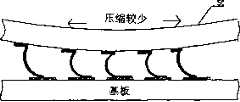
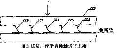
制作电连接到接触垫(例如矽晶圆或基板栅格阵列封装上的金属垫)时,在接触元件接合(engage)这些垫的时候,利用擦刮(wiping)动作和穿入(piercing)动作是很重要的,以突破任何氧化物、有机材料、或其它可能出现在金属垫表面的膜,否则那些膜可能会阻碍电连接。图1例示一接触元件,用以接合基板上的金属垫。参照图1,连接器10包含接触元件12,供电连接至基板14上之金属垫16。连接器10可为晶圆探针卡,则接触元件12为探针尖(tip),供接合矽基板14上之垫16。在正常处理与储存状况下,膜18(其可为氧化物膜或有机膜)形成在金属垫16的表面上。当接触元件12接合金属垫16,接触元件必须穿入膜18,以形成到金属垫16之可靠电连接。膜18之穿入可源自接触元件接合金属垫时,接触元件12之擦刮动作或穿入动作。When making electrical connections to contact pads (such as metal pads on silicon wafers or substrate grid array packages), use wiping and piercing actions when contact elements engage these pads It is important to break through any oxides, organic materials, or other films that may be present on the surface of the metal pads, or those films may prevent electrical connections. FIG. 1 illustrates a contact element for bonding a metal pad on a substrate. Referring to FIG. 1 , a
当需要提供擦舌刮或穿入动作时,重要的是具有受良好控制的擦刮或穿入动作,在制作垫接触时,使其够强以穿过表面膜,但够柔以避免伤害金属垫。此外,重要的是任何擦刮动作提供一足够的擦刮距离,以暴露足够的金属表面,而有良好的电连接。When it is necessary to provide a tongue scraping or penetrating action, it is important to have a well controlled scraping or penetrating action when making pad contact so that it is strong enough to penetrate the surface membrane but soft enough to avoid damaging the metal pad. In addition, it is important that any wiping action provide a sufficient wiping distance to expose enough of the metal surface for a good electrical connection.
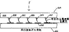
类似地,制作接触至焊料球(如形成在球栅格阵列封装、晶片级封装、或晶圆级封装上的焊料球)时,重要的是提供擦舌刮或穿入动作,以突破焊料球上的原生氧化层(native oxide),以制造良好电接触至焊料球。然而,当使用传统方法来制造电接触至焊料球时,可能伤害或完全从封装移除焊料球。图2A例示一接触元件,用以接触焊料球。当接触元件12接触形成在例如供测试之基板20上的焊料球22时,接触元件12利用穿入动作,通常导致焊料球之顶表面(亦称基【base】表面)形成一凹坑(crater)。当包含焊料球22之基板20接着依附于另一半导体装置(如PC板或晶片级封装),焊料球22中的凹坑会导致焊料球接口形成空洞(void)。图2B和图2C例示使焊料球22依附于基板24之金属垫26的结果。在焊料回流(solder reflow)后(图2C),焊料球22依附至金属垫26。然而,在焊料球接口形成一空洞,因为凹坑出现在焊料球22之顶表面上,此凹坑系由接触元件12之穿入动作造成。此类空洞的出现可影响连接的电特性,且更重要地,降低连接的可靠度。Similarly, when making contacts to solder balls (such as those formed on ball grid array packages, wafer level packages, or wafer level packages), it is important to provide a wiping or penetrating action to break through the solder balls The native oxide layer (native oxide) on the surface to make good electrical contact to the solder ball. However, when conventional methods are used to make electrical contacts to the solder balls, the solder balls may be damaged or completely removed from the package. FIG. 2A illustrates a contact element for contacting solder balls. When the
因此,期望提供一种电接触元件,其可提供受控制的擦刮动作于金属垫上,特别是节距小于50微米的垫。亦期望此擦舌11动作提供达50%接触垫的擦挂距离。此外,当制作电接触至焊料球时,期望具有一电接触元件,可提供受控制的擦刮动作于焊料球上,而不伤害焊料球的接触表面。Accordingly, it is desirable to provide an electrical contact element that provides a controlled wiping action on metal pads, especially pads with a pitch of less than 50 microns. It is also expected that this tongue 11 wiping action provides up to 50% of the contact pad wiping distance. Additionally, when making electrical contacts to solder balls, it is desirable to have an electrical contact element that provides a controlled wiping action over the solder balls without damaging the contact surfaces of the solder balls.
电连接器遭遇的另一个问题是共面性(coplanarity)的差异,以及欲连接之半导体装置之接触点的位置失准(misalignment)。举例而言,半导体晶圆和封装制程中的差异,常导致接触点(金属垫或焊料球)最终位置、每一平面尺寸之差异。于接触点阵列中,位置失准导致不同接触点之相对位置的差异。因此,连接器必须可适应源自失准的位置差异,以适用在大部分应用中。所以,期望具有尺寸可缩放(scalable)的电接触元件,其可弹性作用,而能够容忍共面性之正常差异以及接触点之位置失准。Another problem encountered by electrical connectors is the difference in coplanarity and misalignment of the contacts of the semiconductor devices to be connected. For example, differences in semiconductor wafer and packaging processes often lead to differences in the final position of contact points (metal pads or solder balls) and in the dimensions of each plane. In an array of contact points, positional misalignment results in differences in the relative positions of different contact points. Therefore, the connector must accommodate positional differences resulting from misalignment in order to be suitable for most applications. Therefore, it is desirable to have a dimensionally scalable electrical contact element that can act elastically while being able to tolerate normal variations in coplanarity and misalignment of contact points.
提供电连接予半导体装置的连接器或互连系统属已知。举例而言,于2000年3月7日核准给Eldridge等人之美国专利6,032,356号,揭露弹性接触结构之阵列,其系直接装设于半导体晶圆之焊垫(bonding pad)上。接触结构系藉以下形成:附接金接合线至晶圆,塑形接合线,并接着涂覆(overcoating)接合线,以形成复合(composite)接触元件。虽然Eldridge揭露的方法,提供半导体级之全金属接触阵列,其中一次形成一个接触元件,因此接触元件需要昂贵的系列制程。此外,接触结构固有的尖形(pointyshape)导致在制造接触时,穿入动作易于伤害如焊料球之接触点。Connectors or interconnection systems that provide electrical connections to semiconductor devices are known. For example, US Patent No. 6,032,356, issued March 7, 2000 to Eldridge et al., discloses an array of resilient contact structures mounted directly on bonding pads of a semiconductor wafer. Contact structures are formed by attaching gold bond wires to the wafer, shaping the bond wires, and then overcoating the bond wires to form composite contact elements. Although the method disclosed by Eldridge provides an array of all-metal contacts at the semiconductor level, wherein the contact elements are formed one at a time, the contact elements therefore require an expensive serial process. In addition, the inherent pointy shape of the contact structure makes it easy for the penetrating action to damage the contact point, such as a solder ball, when making the contact.
于2001年2月6日核准给Smith等人之美国专利6,184,065号,揭露由薄金属膜中的固有应力梯度(stress)创造的小金属弹簧。Smith的方法提供半导体级的全金属接触阵列。然而,金属弹簧指入欲接触之平面表面,因此当用以探测(probe)焊料球时,易于伤害焊料球。US Patent No. 6,184,065, issued February 6, 2001 to Smith et al., discloses small metal springs created by inherent stress gradients in thin metal films. Smith's approach provides an array of all-metal contacts at the semiconductor level. However, the metal spring points into the planar surface to be contacted, so when used to probe the solder ball, it is easy to damage the solder ball.
于2001年6月26日核准给Khoury等人之美国专利6,250,933号,揭露一种接触结构,其系藉微制造(microfabrication)科技在一半导体基板或其它介电质上产生接触器,且其中每一接触器形状像一桥,具有一或更多的角部(angled portion)支撑一水平接触部。Khoury的方法提供半导体级之全金属接触阵列,但当面对金属垫时,因为接触元件和金属垫平行,仅提供有限的擦刮动作。Khoury藉加上突点(asperities)以及制造不对称结构,以引致擦刮动作,处理缺乏擦刮之问题。然而,熟习此技艺者显而易知的是,此种方式可提供只有接触之整体尺寸的10%或更少的擦刮距离,对良好电连接而言通常是不够的。此外,当接触焊料球阵列时,因为接触面和焊料球阵列平行,Khoury的方式需要焊料球之基表面实际上被接触。这样的接触会导致焊料球基表面上的伤害,其接着会在后续焊料回流期间导致空洞的形成,如图2C所示。U.S. Patent No. 6,250,933, approved to Khoury et al. on June 26, 2001, discloses a contact structure that uses microfabrication technology to produce contacts on a semiconductor substrate or other dielectric, and wherein each A contactor is shaped like a bridge with one or more angled portions supporting a horizontal contact portion. Khoury's approach provides an array of all-metal contacts at the semiconductor level, but only provides limited wiping action when facing metal pads because the contact elements are parallel to the metal pads. Khoury addresses the lack of scraping by adding asperities and creating an asymmetrical structure to induce a scraping action. However, it will be apparent to those skilled in the art that this approach can provide a wiping distance of 10% or less of the overall size of the contact, which is often insufficient for a good electrical connection. Furthermore, when contacting the array of solder balls, the Khoury approach requires the base surface of the solder balls to actually be contacted because the contact surface is parallel to the array of solder balls. Such contact can cause damage on the solder ball base surface, which in turn can lead to void formation during subsequent solder reflow, as shown in Figure 2C.
总结而言,传统连接器使用在小节距尺寸的半导体装置时不符要求。传统连接在提供擦刮/穿入动作而不伤害如焊料球之基表面的接触点方面,亦不符要求。In summary, conventional connectors do not meet the requirements for semiconductor devices with small pitch sizes. Conventional connections also fall short in providing a wipe/pierce action without damaging the contact point on the base surface, such as a solder ball.
发明内容Contents of the invention
根据本发明一实施例,一连接器供电连接形成于一半导体装置上之垫,系包含一基板,以及形成于基板上之导电材料接触元件阵列。每一接触元件包含依附于基板之顶表面的一基部(base portion),以及一曲弹簧部系自基部延伸并具有一末端(distal end)突出于基板之上。曲弹簧部形成为从一接触平面弯开(curve away),并具有一曲率,当接合半导体装置之一个别垫时,用以提供一受控制的擦刮动作。According to an embodiment of the present invention, a connector power supply connection formed on a pad on a semiconductor device includes a substrate, and an array of conductive material contact elements formed on the substrate. Each contact element includes a base portion attached to the top surface of the substrate, and a curved spring portion extends from the base portion and has a distal end protruding above the substrate. The curved spring portion is formed to curve away from a contact plane and has a curvature for providing a controlled wiping action when engaging an individual pad of the semiconductor device.
根据本发明之另一方面,一种形成包含接触元件阵列的连接器的方法,包含:提供一基板,形成一支撑层于基板上,图案化支撑层以定义一支撑元件阵列,等向蚀刻支撑元件阵列以在每一支撑元件顶上形成圆角(rounded corners),形成一金属层于基板上与支撑元件阵列上,以及图案化金属层以定义一接触元件阵列,其中每一接触元件包含一第一金属部于基板上,以及一第二金属部延伸自第一金属部并部分横过一个别支撑元件之顶部。此方法更包含移除支撑元件阵列。如此形成之接触元件阵列之每一个包含一基部依附于基板,以及一曲弹簧部从基部延伸、并具有一末端突出于基板之上。相对基板表面,曲弹簧部形成为具有一凹(concave)曲率。According to another aspect of the present invention, a method of forming a connector comprising an array of contact elements, comprising: providing a substrate, forming a support layer on the substrate, patterning the support layer to define an array of support elements, isotropically etching the support array of elements to form rounded corners on top of each support element, forming a metal layer on the substrate and the array of support elements, and patterning the metal layer to define an array of contact elements, wherein each contact element includes a The first metal portion is on the substrate, and a second metal portion extends from the first metal portion and partially crosses the top of a respective supporting element. The method further includes removing the array of support elements. Each of the contact element arrays thus formed includes a base attached to the substrate, and a curved spring portion extending from the base and having an end protruding above the substrate. The curved spring portion is formed to have a concave curvature with respect to the substrate surface.
根据本发明之另一方面,一种形成包含一接触元件阵列的一连接器的方法,包含:提供一基板,提供一导电黏着层于基板上,形成一支撑层于导电黏着层上,图案化支撑层以定义一支撑元件阵列,等向蚀刻支撑元件阵列以在每一支撑元件顶上形成圆角,形成一金属层于导电黏着层上与支撑元件阵列上,图案化金属层与导电黏着层以定义一接触元件阵列。每一接触元件包含一第一金属部形成于一导电黏着部上,以及一第二金属部延伸自第一金属部并部分横过一个别支撑元件之顶部。此方法更包含移除支撑元件阵列。According to another aspect of the present invention, a method of forming a connector comprising an array of contact elements includes: providing a substrate, providing a conductive adhesive layer on the substrate, forming a support layer on the conductive adhesive layer, patterning support layer to define an array of support elements, isotropically etch the array of support elements to form rounded corners on top of each support element, form a metal layer on the conductive adhesive layer and on the array of support elements, pattern the metal layer and the conductive adhesive layer to define an array of contact elements. Each contact element includes a first metal portion formed on a conductive adhesive portion, and a second metal portion extending from the first metal portion and partially across the top of a respective supporting element. The method further includes removing the array of support elements.
如此形成之接触元件阵列的每一个包含:一基部依附于导电黏着部,其中导电黏着部依附于基板;以及一曲弹簧部从基部延伸、并具有一末端突出于基板之上。相对基板表面,曲弹簧部形成为具有一凹曲率。Each of the thus formed contact element arrays includes: a base attached to the conductive adhesive, wherein the conductive adhesive attached to the substrate; and a curved spring extending from the base and having an end protruding above the substrate. The curved spring portion is formed to have a concave curvature with respect to the surface of the substrate.
考虑以下详细说明与所附图式时,会更了解本发明。The invention will be better understood upon consideration of the following detailed description and accompanying drawings.
附图说明Description of drawings
图1例示一接触元件,用以接合基板上的金属垫。图2A例示一接触元件,用以接触焊料球。FIG. 1 illustrates a contact element for bonding a metal pad on a substrate. FIG. 2A illustrates a contact element for contacting solder balls.
图2B和图2C例示附接焊料球至基板之金属垫的结果。2B and 2C illustrate the results of attaching solder balls to metal pads of the substrate.
图3A和3B为根据本发明之一实施例,显示连接器之剖面图。3A and 3B are cross-sectional views showing a connector according to an embodiment of the present invention.
图4A和4B为剖面图,例示使用图3A之连接器接合不同半导体装置。4A and 4B are cross-sectional views illustrating the use of the connector of FIG. 3A to join different semiconductor devices.
图5A和5B例示根据本发明之另一实施例之连接器。5A and 5B illustrate a connector according to another embodiment of the present invention.
图6A和6B例示根据本发明之另一实施例之连接器。6A and 6B illustrate a connector according to another embodiment of the present invention.
图7A至7H例示根据本发明之一实施例,形成图3A之连接器的制程步骤。7A to 7H illustrate process steps for forming the connector of FIG. 3A according to one embodiment of the present invention.
图8A至8H例示根据本发明之一实施例,形成图5A之连接器的制程步骤。8A to 8H illustrate process steps for forming the connector of FIG. 5A according to one embodiment of the present invention.
图9A至9H例示根据本发明之另一实施例,形成图5A之连接器的制程步骤。9A to 9H illustrate process steps for forming the connector of FIG. 5A according to another embodiment of the present invention.
图10A和10B为根据本发明之另一实施例之一连接器的剖面图。10A and 10B are cross-sectional views of a connector according to another embodiment of the present invention.
图11为根据本发明之一实施例之连接器的剖面图,此连接器包含供改善信号完整性以及供控制接触元件阻抗之接地平面。11 is a cross-sectional view of a connector including a ground plane for improving signal integrity and for controlling contact element impedance in accordance with one embodiment of the present invention.
图12例示本发明连接器之另一实施例,其中使用一对接触元件耦合至一对差动信号。Figure 12 illustrates another embodiment of the connector of the present invention in which a pair of contact elements is used to couple to a pair of differential signals.
图13例示根据本发明之一实施例,显示包含热导平面之连接器。Figure 13 illustrates a connector including a thermally conductive plane, according to one embodiment of the present invention.
图14例示根据本发明之一实施例,显示包含同轴接触元件的连接器。Figure 14 illustrates a connector including coaxial contact elements according to one embodiment of the present invention.
图15A至15H例示根据本发明之另一实施例,一形成连接器阵列之制程步骤。15A to 15H illustrate a process step for forming a connector array according to another embodiment of the present invention.
具体实施方式Detailed ways
根据本发明之原理,一种提供可分离且可重复装设之连接至一装置的连接器,包含一接触元件阵列形成于一基板上,其中每一接触元件包含一曲弹簧部形成为从一接触平面弯开,并具一曲率,当接合装置之一接触点时,用以提供一受控制的擦刮动作。本A明之连接器可用以电连接至半导体级装置:(如矽晶圆或封装的积体电路)。形成的接触元件可电连接至具250微米或更小节距的接触点,且特别地是,本发明之接触元件可电连接至具50微米或更小节距的接触点。藉由提供受控制的擦刮动作,本发明之连接器可用以连接至不同接触表面,而不伤害接触表面。最后,本发明连接器中的接触元件具有大的弹性工作范围,约等于或大于电路枉长度,藉此容许接触元件在一般操作状况中常需要的大范围压缩(compressions)上操作。According to the principles of the present invention, a connector for providing a detachable and reinstallable connection to a device includes an array of contact elements formed on a substrate, wherein each contact element includes a curved spring portion formed from a The contact plane bends away and has a curvature for providing a controlled wiping action when engaging a contact point of the device. The connector of this invention can be used to electrically connect to semiconductor level devices: (such as silicon wafers or packaged integrated circuits). The formed contact elements can be electrically connected to contacts having a pitch of 250 microns or less, and in particular, the contact elements of the present invention can be electrically connected to contacts having a pitch of 50 microns or less. By providing a controlled wiping action, the connector of the present invention can be used to connect to different contact surfaces without damaging the contact surfaces. Finally, the contact elements in the connector of the present invention have a large elastic operating range, about equal to or greater than the circuit length, thereby allowing the contact elements to operate over the wide range of compressions often required in typical operating conditions.
相较于传统连接器系统,本发明之连接器提供许多的优点。第一,本发明之连接器包含接触元件,系具有一曲弹簧部弯离一接触平面(亦即将接触的接触点表面)。因此,当接合金属垫或焊料球时,接触元件可提供柔性(soft)控制的擦刮动作,容许有效的电连接而不伤害接触表面。再者,本发明之连接器中的接触元件,以最佳接触力可达到最佳的擦刮距离。传统连接器通常包含弯入接触平面的曲弹簧构件(member)。当此类弹簧构件接合一接触垫时,这样的曲率导致一穿入动作,且通常对垫造成所不欲之伤害。选替地,在其它传统连接器中,接触元件不是没提供擦刮动作就是擦刮距离不足。本发明之连接器克服许多传统连接器之缺点。The connector of the present invention provides many advantages over conventional connector systems. First, the connector of the present invention includes a contact element having a curved spring portion bent away from a contact plane (ie, the surface of the contact point to be contacted). Accordingly, the contact elements may provide a soft controlled wiping action when engaging metal pads or solder balls, allowing an effective electrical connection without damaging the contact surfaces. Furthermore, the contact element in the connector of the present invention can achieve an optimal wiping distance with an optimal contact force. Conventional connectors typically include curved spring members that bend into the contact plane. When such a spring member engages a contact pad, such curvature results in a piercing action and often undesired damage to the pad. Alternatively, in other conventional connectors, the contact elements either provide no wiping action or an insufficient wiping distance. The connector of the present invention overcomes many of the disadvantages of conventional connectors.
第二,本发明之连接器提供尺寸可缩放、低轮廓(profile)、低插入力(insertion force)、高密度、以及可分离/可重复连接的电连接,且特别地适用于高速和高性能应用。此连接器可以相对低成作,而展现高度可靠且符合操作特性。特别地是,本发明之连接器可调整尺寸,以接触晶圆上之金属垫或基板栅格阵列封装之基板(lands),其中垫或基板以50微米或更小的节距分隔。本发明之连接器亦可调整尺寸,以接触球栅格阵列封装之焊料球或形成在晶圆上的焊料球,其中焊料球以250微米或更小之节距分隔。Second, the connector of the present invention provides scalable, low profile, low insertion force, high density, and separable/repeatable electrical connections, and is particularly suitable for high speed and high performance application. The connector can be made relatively inexpensively, yet exhibits highly reliable and consistent operational characteristics. In particular, the connectors of the present invention can be sized to contact metal pads on a wafer or lands of a LGA package, where the pads or lands are separated by a pitch of 50 microns or less. The connector of the present invention can also be sized to contact solder balls of a ball grid array package or formed on a wafer, where the solder balls are separated by a pitch of 250 microns or less.
第三,本发明之连接器可用以接合半导体装置之垫,其中垫系和连接的接触元件直立对准。因此,只需要应用一直立外部偏力(biasing force)连接连接器至欲连接的装置。此与许多传统连接器系统相反,其需要应用一横向(lateral)力接合一连接器,且常对连接点导致伤害。Third, the connector of the present invention can be used to engage pads of semiconductor devices, wherein the pads are in upright alignment with the connected contact elements. Therefore, only a vertical external biasing force needs to be applied to connect the connector to the device to be connected. This is in contrast to many conventional connector systems, which require the application of a lateral force to engage a connector and often result in damage to the connection point.
本发明之连接器可用以电连接至广泛种类的装置。举例而言,本发明之连接器可用以电连接至一矽晶圆上之金属垫、一球栅格阵列封装、一基板栅格阵列封装、一晶圆级封装、一晶片级封装和其它半导体或电气装置。本说明中,「装置」一词意指需要电连接或互连的电子装置或组件之类。因此,半导体装置可包含但不限于半导体晶圆、封装的或未封装的积体电路,形成在半导体晶圆上或形成为积体电路封装的球栅格阵列、基板栅格阵列系形成在半导体晶圆上、在晶片模块上、或在积体电路封装上。The connector of the present invention can be used to electrically connect to a wide variety of devices. For example, the connector of the present invention can be used to electrically connect to metal pads on a silicon wafer, a ball grid array package, a land grid array package, a wafer level package, a wafer level package and other semiconductor or electrical installations. In this description, the term "device" means an electronic device or component that requires electrical connection or interconnection. Accordingly, semiconductor devices may include, but are not limited to, semiconductor wafers, packaged or unpackaged integrated circuits, ball grid arrays, substrate grid arrays formed on semiconductor wafers or as integrated circuit packages formed on semiconductor On a wafer, on a chip module, or on an integrated circuit package.
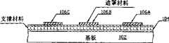
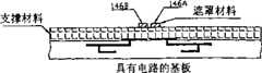
图3A和3B为根据本发明之一实施例,显示一连接器之剖面图。图3A和3B例示本发明之一连接器50,连接至一半导体装置60,其包含金属垫64,系形成在一基板62上做为接触点。半导体装置60可为一矽晶圆,其中金属垫64为形成在晶圆上的金属焊垫。半导体装置60亦可为一基板栅格阵列封装,其中金属垫64代表形成在基板栅格阵列封装上的「基板(lands)」或金属连接垫。图3A和3B中连接器50耦合至半导体装置60只为例示说明,而不欲限制连接器50只应用在与晶圆或基板栅格阵列封装连接。3A and 3B are cross-sectional views showing a connector according to an embodiment of the present invention. 3A and 3B illustrate a
参照图3A,连接器50包含接触元件阵列54,形成在一基板52上。基板52可为一介电材料或一半导体材料。因为连接器50可用以连接至半导体级的半导体装置,通常使用半导体制程常用的材料形成连接器50。于一实施例中,基板50由石英、矽或陶瓷晶圆形成,而接触元件54形成于一介电层上,介电层可为蓝宝石上矽(SOS)、玻璃上矽(SOG)、硼磷四乙基正矽酸盐(BPTEOS)、或四乙基正矽酸盐(TEOS)层,系形成在基板之顶表面上。接触元件阵列一般形成为二维阵列,配置成与将接触的半导体装置上对应的接触点配对。于一实施例中,连接器50系形成以接触具50微米或更小节距的金属垫。Referring to FIG. 3A , the
接触元件54系利用导电材料形成。每一接触元件54包含一基部55A依附于基板52之顶表面,以及一曲弹簧部55B伸自基部55A。曲弹簧部55B具一近端(proximal end)邻近基部55A,以及一末端(distal end)突出于基板52之上。注意图3A和3B例示连接器50为颠倒状,以接合半导体装置60。本说明中方向性词汇之使用,如「上」、「顶表面」,意欲描述当连接器放置成接触元件面朝上时,连接器元件的位置关系。熟此技艺者会理解文中使用之方向性词汇只为例示说明,且只欲描述接触元件不同部分之相对位置。The contact element 54 is formed using a conductive material. Each contact element 54 includes a base portion 55A attached to the top surface of the substrate 52, and a curved spring portion 55B extending from the base portion 55A. The curved spring portion 55B has a proximal end adjacent to the base portion 55A, and a distal end protruding above the base plate 52 . Note that FIGS. 3A and 3B illustrate that the
仍参照图3A,接触元件54包含曲弹簧部,形成为从一接触平面弯开。本说明中,「接触平面」意指接触元件将接触之接触点表面。本例示中,接触平面为金属垫64之表面。如图3A所示,曲弹簧部55B相对于基板52表面,系形成为具有一凹面曲率(concave curvature)。因此曲弹簧部55B系自金属垫64表面弯开。接触元件54之曲弹簧部55B具一曲率,当接合欲接触半导体装置之一个别金属垫64时,用以提供一受控制的擦刮动作。Still referring to FIG. 3A , the contact element 54 includes a curved spring portion formed to bend away from a contact plane. In this description, "contact plane" means the surface of the contact point that the contact element will contact. In this example, the contact plane is the surface of the metal pad 64 . As shown in FIG. 3A , the curved spring portion 55B is formed to have a concave curvature relative to the surface of the substrate 52 . Therefore, the curved spring portion 55B is bent away from the surface of the metal pad 64 . The curved spring portion 55B of the contact element 54 has a curvature to provide a controlled wiping action when engaging a respective metal pad 64 intended to contact a semiconductor device.
于操作中,施加一外部偏力(于图3A中标为F)至连接器50,使得连接器50压缩着半导体装置60之金属垫64。接触元件54之曲弹簧部以一受控制的擦刮动作接合个别金属垫,使得每一接触元件制造有效的电连接至个别的垫。接触元件54之曲率确保同时达到最佳的接触力和最佳的擦刮距离。擦刮距离系当接触金属垫时,接触元件之末端在金属垫之表面所做的移动(travel)量。一般而言,接触力可为5至100克的等级,其视应用而定,而擦刮距离可为5至400微米的等级。In operation, an external biasing force (labeled F in FIG. 3A ) is applied to the
本发明接触元件之另一特征为:接触元件之曲弹簧部可有非常大的弹性工作范围。具体而言,因为曲弹簧部可在直立和水平两个方向移动,可达到接触元件之电路径长度等级的弹性工作范围。本说明中,接触元件之「电路径长度」定义为电流从曲弹簧部之末端至接触元件之基部行经的距离。基本上,本发明之连接器的接触元件具有横跨接触元件整个长度的弹性工作距离。Another feature of the contact element of the present invention is that the curved spring portion of the contact element can have a very large elastic working range. Specifically, since the curved spring portion can move in both vertical and horizontal directions, an elastic working range in the order of the electrical path length of the contact element can be achieved. In this description, the "electrical path length" of a contact element is defined as the distance that the current travels from the end of the curved spring portion to the base of the contact element. Basically, the contact element of the connector of the present invention has a resilient working distance spanning the entire length of the contact element.
接触元件54系利用一导电金属形成,其亦可提供所欲弹性。于一实施例中,接触元件54系利用钛作为支撑结构而形成,此支撑结构稍后可被电镀(plated)以获得所欲弹性行为。于其它实施例中,接触元件54系利用以下形成:铜合金或多层金属片(sheet),如不镌钢涂覆铜一镍一金(Cu/Ni/Au)多层金属片。于一较佳实施例中,接触元件系利用以下形成:一小粒(small-grained)铜一铍(CuBe)合金接着镀上无电(electroless)镍一金(Ni/Au),以提供一不氧化表面。进一步,于另一实施例中,接触元件54于基部和曲弹簧部系使用不同金属形成。The contact element 54 is formed using a conductive metal, which also provides the desired elasticity. In one embodiment, the contact element 54 is formed using titanium as a support structure that can be plated later to obtain the desired elastic behavior. In other embodiments, the contact elements 54 are formed using copper alloys or multilayer metal sheets, such as stainless steel coated copper-nickel-gold (Cu/Ni/Au) multilayer metal sheets. In a preferred embodiment, the contact elements are formed using a small-grained copper-beryllium (CuBe) alloy followed by electroless nickel-gold (Ni/Au) plating to provide an oxidized surface. Further, in another embodiment, the contact element 54 is formed using different metals for the base portion and the curved spring portion.
图3A所示实施例中,接触元件54显示为由一矩形基部和一曲弹簧部形成。此配置只作为例示而不欲作为限制。本发明之接触元件可以多种配置形成,且每一接触元件只需有足以附接曲弹簧部至基板的基部。基部可采用任何形状,而可形成为圆形或其他有用的形状,以附接接触元件至基板。此外,一接触元件可包含多个曲弹簧部延伸自基部,将如以下详加讨论。In the embodiment shown in FIG. 3A, the contact element 54 is shown formed from a rectangular base and a curved spring portion. This configuration is illustrative only and not intended to be limiting. The contact elements of the present invention can be formed in a variety of configurations, and each contact element need only have a base sufficient to attach the curved spring portion to the substrate. The base may take any shape and may be formed as a circle or other useful shape for attaching the contact elements to the substrate. Additionally, a contact element may include a plurality of curved spring portions extending from the base portion, as discussed in more detail below.
本发明之连接器的大弹性工作范围,使得连接器可适应欲连接半导体装置中的正常共面性差异和位置失准。因此,尽管欲连接的半导体装置中可能存在不规则的共面性和位置,连接器可提供可靠的电连接。图4A和4B为剖面图,显示使用连接器50接合不同的半导体装置。图4A中,欲接触的金属垫之位置差异,需要连接器50之一端的接触元件比另一端的接触元件压缩更多。图4B中,欲接触的金属垫之共面性差异,需要连接器50中间部份的接触元件比接触器50两端的接触元件压缩更多。因为本发明的接触元件具有大的弹性工作范围,不同的接触元件可为不同程度的压缩,而所有接触元件提供有效的电连接。The large elastic working range of the connector of the present invention enables the connector to adapt to normal coplanarity differences and positional misalignments in the semiconductor devices to be connected. Thus, the connector can provide a reliable electrical connection despite possible irregularities in coplanarity and position in the semiconductor devices to be connected. 4A and 4B are cross-sectional views showing the use of a
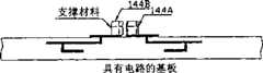
图5A和5B例示根据本发明另一实施例之一连接器。参照图5A,连接器70包含接触元件74之阵列形成在基板72上。本实施例中,每一接触元件74包含一基部75A和二个曲弹簧部75B与75C延伸自基部75A。曲弹簧部75B与75C具有末端突出于基板72之上,并朝向彼此。曲弹簧部75B与75C的其它特性和曲弹簧部55B相同。亦即,曲弹簧部75B与75C形成为从一接触平面弯开,且各具有一曲率,当接合一欲接触的半导体装置之接触点时,以提供受控制的擦刮动作。再者,曲弹簧部75B与75C具有大弹性工作范围,约等于接触元件之电路径长度,藉此容许用于大范围压缩。5A and 5B illustrate a connector according to another embodiment of the present invention. Referring to FIG. 5A , a
于本例示中,连接器70用以接触一半导体装置80,例如一球栅格阵列封装,包含焊料球84之阵列作为接触点。图5B例示连接器70完全接合半导体装置80。连接器70可用以接触金属垫,例如基板栅格阵列封装上的垫。然而,使用连接器70接触焊料球84提供特别的优点。In this illustration, the
第一,接触元件74沿着焊料球的侧边接触个别焊料球。不接触焊料球之基表面。因此,于接触期间,接触元件74不会伤害焊料球之基表面,且有效消除焊料球为永久附接于后续回流时,形成空洞的可能性。First, contact
第二,因为接触元件74之每一曲弹簧部形成为从接触平面弯开,本例中接触平面是与欲接触的焊料球之侧表面相切的平面,当接触个别焊料球时,接触元件74提供受控制的擦刮动作。以此方式,可做有效电连接而不伤害接触表面,亦即焊料球之表面。Second, because each curved spring portion of the
第三,连接器70尺寸可缩放,且可用以接触具250微米或更小之节距的焊料球。Third, the
最后,因为每一接触元件具有电路径长度等级的大弹性工作范围,接触元件可适应大范围压缩。因此,本发明之连接器可有效地用以接触具正常共面性差异或位置失准的传统装置。Finally, because each contact element has a large elastic operating range on the order of the electrical path length, the contact elements can accommodate a wide range of compressions. Therefore, the connector of the present invention can be effectively used to contact conventional devices with normal coplanarity variance or misalignment.
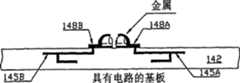
图3A和5A中的连接器50和70显示为包含一曲弹簧部线性地从基部突出。图3A和5A所示实施例仅为例示而不欲作为限制。本发明之连接器可以多种方式配置,视欲接触的接触点类型而定,且视所欲接触力而定。图6A和6B例示根据本发明另一实施例之连接器。参照图6A,一连接器90包含一接触元件93形成在基板92上。接触元件93包含一基部94A和一第一曲弹簧部94B,以及一第二曲弹簧部94C。第一曲弹簧部94B和第二曲弹簧部94C具有彼此指离的末端。接触元件93可用以接合一接触点,包含一金属垫或一焊料球。当用以接合一焊料球,接触元件93在第一与第二曲弹簧部问支托住焊料球。因此,第一和第二曲弹簧部94B和94C以从焊料球之接触平面弯开的方向,用一受控制的擦刮动作接触焊料球之侧表面。
图6B例示一接触元件95形成在基板96上。接触元件95包含一基部97A,和一第一曲弹簧部97B以及一第二曲弹簧部97C伸自基部。本实施例中,第一曲弹簧部97B和第二曲弹簧部97C以螺旋(spiral)配置突出于基板96之上。接触元件95可用以接触一金属垫或一焊料球。于两种情形中,第一和第二曲弹簧部97B和97C从接触平面弯开,并提供一受控制的擦刮动作。FIG. 6B illustrates a contact element 95 formed on a substrate 96 . The contact element 95 includes a base portion 97A, and a first curved spring portion 97B and a second curved spring portion 97C extend from the base portion. In this embodiment, the first curved spring portion 97B and the second curved spring portion 97C protrude above the base plate 96 in a spiral configuration. The contact element 95 can be used to contact a metal pad or a solder ball. In both cases, the first and second curved spring portions 97B and 97C bend away from the contact plane and provide a controlled wiping action.
本发明之连接器可使用不同制程顺序,以多种制程制造。举例而言,每一接触元件之曲弹簧部可由模锻(stamping)形成。于一实施例中,本发明之连接器系利用半导体制程技术形成。当利用半导体制程技术形成时,本发明之连接器可称之作为微机电系统(MEMS)。因此,于本发明一实施例中,本发明之连接器亦称做一微机电系统栅格阵列连接器。The connector of the present invention can be manufactured in various processes using different process sequences. For example, the curved spring portion of each contact element may be formed by stamping. In one embodiment, the connector of the present invention is formed using semiconductor process technology. When formed using semiconductor process technology, the connector of the present invention may be referred to as a micro-electro-mechanical system (MEMS). Therefore, in an embodiment of the present invention, the connector of the present invention is also called a MEMS grid array connector.
图7A至7H例示根据本发明之一实施例,形成图3A之连接器50的制程步骤。参照图7A,提供一基板102,接触元件将形成于其上。基板102可例如为一矽晶圆或陶瓷晶圆,且可包含一介电层形成于其上(未示于图7A)。如上所述,SOS、SOG、BPTEOS、或TEOS层之一介电层,可形成于基板102上,以隔离基板102及接触元件。接着,一支撑层104形成于基板102上。支撑层104可为一沉积介电层,例如气化物或氮化物层、旋转涂布(spin-on)介电质、聚合物、或任何其它可适合蚀刻的材料。于一实施例中,支撑层104系由化学气相沉积制程沉积。另一实施例中,支撑层104系由电浆气相沉积(plasma vapor,PVD)制程沉积。又另一实施例中,支撑层104系由旋转涂布制程沉积。再另一实施例中,当基板102未覆有介电层或导电黏着层时,支撑层可利用半导体制程常使用的氧化制程成长。7A to 7H illustrate process steps for forming the
支撑层104沉积后,遮罩层106形成于支撑层104之顶表面上。遮罩层106结合传统微影制程,以利用遮罩层106定义图案(pattern)于支撑层104上。在遮罩层打印(printed)与显影(developed)后(图7B),包含区域106A至106C之遮罩图案,形成在支撑层104之表面上定义支撑层104受保护而免于后续蚀刻之区域。After the
参照图7C,利用区域106A至106C作为遮罩,执行一非等向蚀刻制程。非等向蚀刻制程的结果,移除图案化遮罩层未覆盖的支撑层104。因此,形成支撑区域104A至104C。接着移除包含区域106A至106C的遮罩图案,以暴露支撑区域(图7D)。Referring to FIG. 7C, an anisotropic etching process is performed using the
参照图7E,支撑区域104A至104C接着经历一等向蚀刻制程。等向蚀刻制程以实质上相同的蚀刻速率,在直立和水平方向移除受蚀刻之材料。因此,等向蚀刻之结果,削圆支撑区域104A至104C的顶角,如图7E所示。于一实施例中,等向蚀刻制程为电浆蚀刻制程,使用SF6、CHF3、CF4或其它蚀刻介电材料常用的习知化学物。另一实施例中,等向蚀刻制程为湿蚀刻制程,例如使用缓冲气化物蚀刻(BOE)之湿蚀刻制程。Referring to FIG. 7E , the
接着,参照图7F,一金属层108形成于基板102之表面和支撑区域104A至104C之表面上。金属层108可为铜层或铜合金层或多层金属沉积,如镀上铜一镍一金(Cu/Ni/Au)的钨。一较佳实施例中,接触。元件系利用以下形成:一小粒铜一铍(CuBe)合金,接着镀以无电镍一金(Ni/Au),以提供一不气化表面。金属层108可以利用化学气相沉积制程、电镀、溅镀、物理气相沉积来沉积,或其它习知金属膜沉积技术。利用传统微影制程,沉积一遮罩层且图案化为遮罩区域110A至110C。遮罩区域110A至110C定义金属层108受保护而免于后续蚀刻之区域。Next, referring to FIG. 7F , a metal layer 108 is formed on the surface of the
接着,图7F的结构经历一蚀刻制程,以移除未被遮罩区域110A至110C覆盖的金属层。结果,形成金属部108A至108C,如图7G所示。金属oP 108A至108C之每一个,包含一基部形成在基板102上,以及一曲弹簧部形成在个别的支撑区域(104A至104C)上。因此,每一金属部之曲弹簧部采取其下支撑区域的形状,突出于基板表面之上,并具一曲率,当接触一接触点时,提供一擦刮动作。Next, the structure of FIG. 7F undergoes an etching process to remove the metal layer not covered by the mask regions 110A to 110C. As a result,
为完成连接器,移除支撑区域104A至104C(图7H),使用如湿蚀刻或非等向电浆蚀刻或其它蚀刻制程。若支撑层使用氧化层形成,可使用缓冲氧化物蚀刻剂(etchant)移除支撑区域。结果,形成独立的(freestanding)接触元件112A至112C在基板102上。To complete the connector,
熟此技艺者知悉本发明时,理解要制作本发明之连接器,上述制程步骤可能有许多变化。举例而言,等向性蚀刻制程的化学物和蚀刻条件可加以修改,以在支撑区域提供所欲形状,使得形成的接触元件有所欲曲率。进一步而言,熟此技艺者会理解,透过使用半导体制程技术,可制造连接器之接触元件具多种性质。举例而言,第一群组的接触元件可形成为具有第一节距,而第二群组的接触元件可形成为具有大于或小于第一节距之第二节距。接触元件之电或机械性质可能有其它变化,如以下将详加描述。When those skilled in the art know the present invention, they will understand that there may be many variations of the above-mentioned process steps in order to make the connector of the present invention. For example, the chemistry and etch conditions of an isotropic etch process can be modified to provide a desired shape in the support region such that the formed contact elements have a desired curvature. Further, those skilled in the art will understand that by using semiconductor process technology, it is possible to manufacture the contact elements of the connector with various properties. For example, a first group of contact elements may be formed with a first pitch, and a second group of contact elements may be formed with a second pitch that is greater or smaller than the first pitch. Other variations in the electrical or mechanical properties of the contact elements are possible, as will be described in more detail below.
图8A至8H例示根据本发明之一实施例,形成图5A之连接器70的制程步骤。图8A至8H所示之制程步骤和图7A至7H所示制程步骤实质上相同。然而,图8A至8H例示藉由适当设计的遮罩图案,可制造不同配置的接触元件。8A to 8H illustrate process steps for forming the
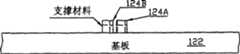
参照图8A,一支撑层124形成于基板122上。一遮罩层126形成于支撑层上,供定义形成图5A之连接器所欲遮罩区域。本实施例中,遮罩区域126A和126B(图8B)位置靠在一起,以容许形成包含两个曲弹簧部的接触元件。Referring to FIG. 8A , a supporting
利用遮罩区域126A和126B作为遮罩,执行一非等向蚀刻制程后,形成支撑区域124A和124B(图8C)。移除遮罩区域以暴露支撑区域(图8D)。接着,支撑区域124A和124B经历等向蚀刻制程以使结构成形,使得支撑区域之顶表面包含圆角(图8E)。Using the mask regions 126A and 126B as masks, an anisotropic etching process is performed to form the
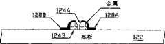
一金属层128沉积于基板122之表面和支撑区域124A和124B之顶表面上方(图8F)。包含区域130A和130B之遮罩图案,定义在金属层128上。利用遮罩区域130A和130B作为遮罩,蚀刻金属层128后,形成金属部128A和128B(图8G)。每一金属部128A和128B包含一基部形成于基板122上,以及一曲弹簧部形成于个别支撑区域(124A或124B)上。每一金属部之曲弹簧部采取其下支撑区域的形状,突出于基板表面之上,并具有一曲率,当接触一接触点时,提供一擦刮动作。本实施例中,金属部128A和128B的末端形成为彼此面对。为完成此连接器,移除支撑区域124A至124B(图8H)。结果,形成独立的接触元件132在基板102上。在图8H之剖面图中,接触元件132的二个金属部看似未连接。然而,实际实作中,金属部之基部藉由像是形成一环(ring)环绕接触元件而连接,或是基部可透过形成于基板122中的导电层而连接。A metal layer 128 is deposited over the surface of
图9A至9H例示根据本发明之另一实施例,形成图5A之连接器70的制程步骤。参照图9A,提供包含预定义电路145的一基板142。预定义电路145可包含互连的金属层或其它电装置,像是电容或电感,这些一般形成在基板142中。本实施例中,一顶金属部147形成在基板142之顶表面上,与将形成的接触元件连接。为形成所欲接触元件,一支撑层144和一遮罩层146形成在基板142之顶表面上。9A to 9H illustrate process steps for forming the
制程步骤以类似上述参照图8A至8H的方式进行。图案化遮罩层146(图9B),而接着蚀刻支撑层144,以形成支撑区域144A和144B(图9C)。移除遮罩区域以暴露支撑区域(图9D)。接着,执行等向蚀刻制程,削圆支撑区域144A和144B的顶角(图9E)。沉积一金属层148在基板142之表面上以及支撑区域上方(图9F)。金属层148形成于顶金属部147上方。结果,金属层148电连接至电路145。The process steps are performed in a manner similar to that described above with reference to FIGS. 8A to 8H .
藉由一遮罩层150图案化金属层148(图9F),并经历一蚀刻制程。因此,形成的金属部148A和148B(图9G)具有指向彼此的末端。移除支撑部144A和144B,以完成接触元件152之制作(图9H)。The metal layer 148 ( FIG. 9F ) is patterned by a mask layer 150 and undergoes an etching process. Thus,
如此形成的接触元件152系电连接电路145。以此方式,本发明之连接器可提供额外的功能性。举例而言,电路145可形成为将某些接触元件电连接在一起。电路145亦可用来连接某些接触元件至电装置,例如形成在基板142中或上的一电容或一电感。The contact element 152 thus formed is electrically connected to the
制作接触元件152作为积体电路制程的一部分提供进一步优点。具体而言,一连续电路径形成于接触元件152和底下的电路145间。接触元件和相关电路问没有金属不连续或阻抗不匹配(impedance mismatch)。某些先前技术连接器中,使用金接合线形成接触元件。然而,这样的结构导致接触元件和底下的金属连接间之介面的总(gross)材料和剖面不连续、以及阻抗不匹配,而导致不期望的电特性以及不良的高频橾作。本发明之接触元件不受传统连接器系统之限制,并且使用本发明之接触元件建立的连接器可用于高要求的高频和高性能应用中。Fabricating the contact elements 152 as part of the integrated circuit process provides further advantages. Specifically, a continuous electrical path is formed between the contact element 152 and the underlying
如上所述,当本发明之连接器的接触元件使用半导体制程形成,可形成具有多种机械和电性质的接触元件。特别地,使用半导体制程步骤容许建立一连接器,而包含具不同机械及/或电性质的接触元件。As mentioned above, when the contact elements of the connector of the present invention are formed using a semiconductor process, contact elements with various mechanical and electrical properties can be formed. In particular, the use of semiconductor processing steps allows the creation of a connector comprising contact elements with different mechanical and/or electrical properties.
因此,根据本发明之另一方面,本发明之连接器之接触元件具有不同操作特性。亦即,连接器包含异质(heterogeneous)接触元件,其中可选择接触元件的操作特性,以满足想要应用的要求。本说明中,一接触元件的操作特性意指接触元件的电、机械和可靠度性质。藉着纳入具不同的电及/或机械性质的接触元件,本发明之连接器可满足高性能互连应用对电、机械和可靠度的严厉需求。Therefore, according to another aspect of the invention, the contact elements of the connector of the invention have different operating characteristics. That is, the connector contains heterogeneous contact elements, wherein the operational characteristics of the contact elements can be selected to meet the requirements of the intended application. In this specification, the operational characteristics of a contact element mean the electrical, mechanical and reliability properties of the contact element. By incorporating contact elements with different electrical and/or mechanical properties, the connectors of the present invention can meet the stringent electrical, mechanical and reliability requirements of high performance interconnection applications.
根据本发明之一实施例,可为一接触元件或一组接触元件特别地设计以下机械性质,以达某些所欲操作特性。第一,可选择每一接触元件之接触力,以确保不管是一些接触元件的低阻值连接或连接器的低整体接触力。第二,接触元件随电性要求操作的每一接触元件之弹性工作范围,在接触元件间是可以变化的。第三,每一接触元件之直立高度可以变化。第四,接触元件之节距或水平尺寸可以变化。According to an embodiment of the present invention, the following mechanical properties may be specifically designed for a contact element or a group of contact elements to achieve certain desired operational characteristics. First, the contact force of each contact element can be selected to ensure a low resistance connection of either a few contact elements or a low overall contact force of the connector. Second, the elastic working range of each contact element in which the contact elements operate with electrical requirements is variable between contact elements. Third, the vertical height of each contact element can vary. Fourth, the pitch or horizontal dimension of the contact elements can vary.
根据本发明另些实施例,可为一接触元件或一组接触元件特别地设计电性质,以达某些所欲操作特性。举例而言,每一接触元件之直流阻值(DCresistance)、阻抗、电感(inductance)和载流能力在接触元件间可变化。因此,一群组的接触元件可设计成有较低阻值,或一群组的接触元件可设计成有低电感。According to other embodiments of the present invention, electrical properties may be specially designed for a contact element or a group of contact elements to achieve certain desired operating characteristics. For example, the DC resistance, impedance, inductance, and current carrying capacity of each contact element can vary between contact elements. Therefore, a group of contact elements can be designed to have lower resistance, or a group of contact elements can be designed to have low inductance.
大部分应用中,接触元件可设计为一接触元件获得所欲可靠度性质,或为一组接触元件达某些所欲橾作特性。举例而言,接触元件可设计成在环境应力(例如热循环、热震和振动【thermal shock and vibration】、腐蚀测试、和湿度测试)后,显示无或最小的性能下降。接触元件亦可设计成达到业界标准定义的其它可靠度要求,例如电子产业联盟(EIA)所定义的。In most applications, a contact element can be designed to achieve desired reliability properties for one contact element, or to achieve certain desired operational characteristics for a group of contact elements. For example, contact elements can be designed to show no or minimal performance degradation after environmental stresses such as thermal cycling, thermal shock and vibration, corrosion testing, and humidity testing. Contact elements may also be designed to meet other reliability requirements defined by industry standards, such as those defined by the Electronic Industries Alliance (EIA).
当本发明之连接器中的接触元件制造为微机电系统栅格阵列,接触元件之机械和电特性可藉改变以下设计参数而修改。第一,可选择接触元件之曲弹簧部的厚度,以产生所欲接触力。举例而言,一般大约30微米的厚度产生10克或更少等级的低接触力,而对相同位移(displacement),40微米的凸缘(flange)厚度产生20克的较高接触力。也可选择曲弹簧部。的宽度、长度和形状,以产生所欲接触力。When the contact elements in the connector of the present invention are fabricated as MEMS grid arrays, the mechanical and electrical characteristics of the contact elements can be modified by changing the following design parameters. First, the thickness of the curved spring portion of the contact element can be selected to produce the desired contact force. For example, typically a thickness of about 30 microns produces a low contact force of the order of 10 grams or less, while a flange thickness of 40 microns produces a higher contact force of 20 grams for the same displacement. Curved springs are also available as an option. width, length and shape to produce the desired contact force.
第二,可选择接触元件中要包含的曲弹簧部数量,以达所欲接触力、所欲载流能力和所欲接触阻值。举例而言,加倍曲弹簧部的数目大约加倍接触力和载流能力,而大约减少一半接触阻值。Second, the number of curved spring portions to be included in the contact element can be selected to achieve the desired contact force, desired current carrying capacity, and desired contact resistance. For example, doubling the number of curved spring portions approximately doubles the contact force and current carrying capacity, while approximately halving the contact resistance.
第三,可选择特殊的金属成分和处理,以获得所欲弹性和导电性特性。举例而言,铜合金,例如铜一铍,可用以提供机械弹性和电传导性间的良好取舍。选替地,可使用金属多层提供优越的机械与电性质两者。一实施例中,一接触元件使用钛镀以铜、接着镀镍、最后镀金,而形成钛/铜/镍/金多层。钛会提供优越的弹性与高的机械耐久性(durability),而铜提供优越的导电性,镍层和金层提供优越的抗腐蚀性(corrosionresistance)。最后,不同的金属沉积技术,例如电镀或溅镀,以及不同的金属处理技术,如合金、退火以及其它冶金技术,可用以为接触元件特别设计所欲特性。Third, special metal compositions and treatments can be selected to obtain desired elastic and conductive properties. For example, copper alloys, such as copper-beryllium, may be used to provide a good trade-off between mechanical elasticity and electrical conductivity. Alternatively, metal multilayers can be used to provide both superior mechanical and electrical properties. In one embodiment, a contact element using titanium is plated with copper, then nickel, and finally gold to form a titanium/copper/nickel/gold multilayer. Titanium will provide superior elasticity and high mechanical durability, while copper will provide superior electrical conductivity, and the nickel and gold layers will provide superior corrosion resistance. Finally, different metal deposition techniques, such as electroplating or sputtering, as well as different metal treatment techniques, such as alloying, annealing and other metallurgical techniques, can be used to specifically design the desired properties for the contact elements.
第四,可设计曲弹簧部之曲率,以产生某种电和机械性质。亦可变化曲弹簧部之高度、或从基部突出的量,以产生所欲电和机械性质。Fourth, the curvature of the curved spring portion can be designed to produce certain electrical and mechanical properties. The height of the curved spring portion, or the amount of protrusion from the base, can also be varied to produce desired electrical and mechanical properties.
图10A和10B为根据本发明之另一实施例之一连接器的剖面图。参照图10A,一连接器220包含一第一组接触元件224、226和228,以及一第二组接触元件225和227,皆形成在基板222上。第一组接触元件224,226和228具有一曲弹簧部长于第二组接触元件225和227之曲弹簧部。换言之,接触元件224、226和228之曲弹簧部的高度大于接触元件225和227之曲弹簧部的高度。10A and 10B are cross-sectional views of a connector according to another embodiment of the present invention. Referring to FIG. 10A , a
藉由提供具不同高度之接触元件,本发明之连接器可有利地应用于「热调换(hot-swapping)」应用中。热调换意指当装置欲连接之系统为电活动(electrically)时,装设或拆卸一半导体装置,而不伤害此半导体装置或系统。于热调换操作中,不同电源和接地接脚及信号接脚必须依序且不同时的连接和切断,以避免伤害装置或系统。藉由使用包含不同高度的接触元件的连接器,较高的接触元件在较短接触元件前,可用以制造电连接。以此方式,可制造所欲电连接顺序,以达热调换操作。By providing contact elements with different heights, the connector of the present invention can be advantageously applied in "hot-swapping" applications. Hot swapping means installing or removing a semiconductor device without damaging the semiconductor device or system when the system to which the device is to be connected is electrically active. During the hot swap operation, different power and ground pins and signal pins must be connected and disconnected sequentially and not at the same time to avoid damage to the device or system. By using a connector that includes contact elements of different heights, taller contact elements can be used to make electrical connections in front of shorter contact elements. In this way, a desired sequence of electrical connections can be made to achieve hot swap operations.
如图10A所示,连接器220欲连接至一半导体装置230,半导体装置230包含形成其上的金属垫232。当施加一外部偏力F接合连接器220与半导体装置230,高接触元件224、226和228可首先接触个别的金属垫232,而较短的接触元件225和227保持未连接。接触元件224、226和228可用以电连接至半导体装置230之电源与接地接脚。藉进一步施加外部偏力F(图IOB),连接至信号接脚之较短的接触元件225和227,则可连接装置230上个别的金属垫232。因为本发明之接触元件具有大弹性工作范围,第一组接触元件可比第二组接触元件进一步压缩,而不影响接触元件之完整性(integrity)。以此方式,连接器220使半导体装置230能热调换操作。As shown in FIG. 10A , the
根据本发明之另一方面,一连接器具有接地平面,且接触元件之阻抗可藉以下方式控制;变化一信号接脚之接触元件与接地平面间的距离,或一信号接脚之接触元件与一接地接脚之接触元件间的距离。图11为根据本发明一实施例之一连接器的剖面图,此连接器包含一接地平面,改善信号完整性以及控制接触元件阻抗。参照图11,一连接器250包含一接触元件254B,其欲连接至一半导体装置上的一信号接脚。连接器250更包含接触元件254C,其欲连接至半导体装置之接地电位。连接器250包含一接地平面255,其形成于基板252中。接地平面255可形成于基板252之顶表面上,或嵌入于基板252中。图11中,显示接触元件254A与254C和接地平面255间的连接。实际实作中,接触元件254A与254C可透过基板252表面上的金属连接,或透过嵌于基板252中的金属连接,与接地平面255连接。According to another aspect of the present invention, a connector has a ground plane, and the impedance of the contact elements can be controlled by varying the distance between the contact elements of a signal pin and the ground plane, or the distance between the contact elements of a signal pin and the ground plane. The distance between contact elements of a ground pin. 11 is a cross-sectional view of a connector including a ground plane to improve signal integrity and control contact element impedance in accordance with an embodiment of the present invention. Referring to FIG. 11, a
连接器250中包含接地平面255,具有改善透过连接器250连接之交流电信号的信号完整性的效果。特别地,随着积体电路操作于愈来愈高的频率,封装接脚(lead)数目随接脚的节距下降而增加,改善用于互连此类积体电路之连接器中的信号完整性的能力变得更重要。根据本发明,连接器250包含接地平面255,其作用以降低噪声以及改善连接器之信号完整性。此外,图11所示配置中,一信号接脚之接触元件254B和接地电位之接触元件254A与254C间的距离G可变化,为接触元件254B获得所欲阻抗。可包含元件257A、257B和257C以进一步控制连接器的电磁放射(emission)和斥拒(rejection)特性。The
图12例示本发明连接器之另一实施例,其中使用一对接触元件262和264以耦合至一对差动信号(differential signals)。本实施例中,接触元件262和264各自形成为包含分离的基部261和263。以此方式,包含接触元件262和264之连接器可用以接触包含一对差动信号的半导体装置。Figure 12 illustrates another embodiment of the connector of the present invention in which a pair of contact elements 262 and 264 are used to couple to a pair of differential signals. In this embodiment, the contact elements 262 and 264 are each formed to include separate bases 261 and 263 . In this way, a connector including contact elements 262 and 264 may be used to contact a semiconductor device including a pair of differential signals.
根据本发明另一方面,一连接器包含埋式散热(thermal dissipation)结构,以在特定接触元件提供加强的散热能力。举例而言,当接合电子封装之接脚的接触元件承载多于1安培的电流,显著的焦耳加热(Joule heating)可导致接触元件处的温度上升20度或更多。根据本发明,包含埋式散热结构之连接器,有效地限制特定接触元件的温度上升。举例而官,藉由使用本发明连接器中的埋式散热结构,温度上升的量可减至10度或更少。According to another aspect of the present invention, a connector includes a thermal dissipation structure to provide enhanced heat dissipation capability at specific contact elements. For example, when a contact element engaging a pin of an electronic package carries more than 1 amp of current, significant Joule heating can cause the temperature at the contact element to rise by 20 degrees or more. According to the present invention, a connector including a buried heat dissipation structure effectively limits the temperature rise of a specific contact element. For example, by using the buried heat dissipation structure in the connector of the present invention, the amount of temperature rise can be reduced to 10 degrees or less.
图13例示根据本发明一实施例,系包含热导平面之连接器。参照图13,连接器270包含接触元件274A至274D,形成于基板272之顶表面上。在基板272之制程期间,热导平面277形成于基板272中。热导平面277提供接触元件274A至274D散热功能。于一实施例中,热导平面使用铜形成。另一实施例中,热导平面使用填充环氧树脂(filled epoxy)形成,其为非导电性,而因此可紧密接触出现在基板272中并连接至接触元件274A至274D的任何电路。操作中,当接触元件耦合至一半导体装置、并经历焦耳加热时,热导平面288散去接触元件产生的热。FIG. 13 illustrates a connector including a thermally conductive plane, according to one embodiment of the present invention. Referring to FIG. 13 ,
根据本发明再另一方面,一连接器包含一或更多同轴(coaxial)接触元件。图14例示根据本发明之一实施例,系包含同轴接触元件的连接器300。参照图14,连接器300包含一第一接触元件320及一第二接触元件340,形成在基板之顶表面上。接触元件320和340形成得彼此邻近但电气隔离。本实施例中,接触元件320包含一基部322形成如包含一孔(aperture)的外环,而接触元件340包含一基部342形成于此开口内。每一接触元件320和340包含多个曲弹簧部。具体地,接触元件320包含八个曲弹簧部324,沿环状基部322散开。曲弹簧部324形成为从基部线性突出。另一方面,接触元件340包含两个曲弹簧部344A和344B,每一曲弹簧部以螺旋配置从基部突出。According to yet another aspect of the present invention, a connector includes one or more coaxial contact elements. FIG. 14 illustrates a
接触元件320之曲弹簧部不和接触元件340之曲弹簧部重叠。因此,接触元件320和接触元件340为电气隔离。如此构成后,连接器300可用以互连一半导体装置上的一同轴连接。一般而言,外部的接触元件耦合至一接地电位连接,而内部的接触元件耦合至一信号连接,例如高频信号。本发明之连接器的一个特别优点是,同轴接触元件可调整至250微米或更小尺寸。因此,本发明之连接器甚至可用以提供小尺寸电子元件的同轴连接。The curved spring portion of the
根据本发明另一方面,连接器之每一捆接触元件更包含一导电黏着层于接触元件之基部中,以改善接触元件对基板之黏着。图15A至15H例示根据本发明另一实施例,形成一连接器阵列之制程步骤。图7A至7H和图15A至15H中类似元件给予类似编号,以简化讨论。According to another aspect of the present invention, each bundle of contact elements of the connector further includes a conductive adhesive layer in the base of the contact elements to improve the adhesion of the contact elements to the substrate. 15A to 15H illustrate process steps for forming a connector array according to another embodiment of the present invention. Similar numbers are given to similar elements in FIGS. 7A-7H and FIGS. 15A-15H to simplify the discussion.
参照图15A,提供一基板102,接触元件将形成于其上。基板102可为一矽晶圆或陶瓷晶圆,且可包含一介电层形成其上(未示于图15A中)。一导电黏着层103沉积于基板102上,或假如有介电层,则于介电层顶上。导电黏着层103可为一金属层,例如铜一铍或钛,或导电的聚合物为基础之黏着剂,或其它导电黏着剂。接着,一支撑层104形成于黏着层103上。支撑层104可为沉积的介电层,例如气化层或氮化层,旋转涂布介电质,聚合物,或任何其它适合的可蚀刻材料。Referring to Figure 15A, a
在沉积支撑层104后,一遮罩层106形成于支撑层104之顶表面上。遮罩层106结合传统微影制程的使用,以遮罩层106定义一图案于支撑层104上。在遮罩层打印与显影后(图15B),包含区域106A至106C之遮罩图案,形成在支撑层104之表面上,定义支撑层104受保护而免于后续蚀刻之区域。After depositing the
参照图15C,利用区域106A至106C做为遮罩,执行一非等向蚀刻制程。非等向蚀刻制程的结果是,移除未被图案化遮罩层覆盖的支撑层104。非等向蚀刻制程停在导电黏着层103上,或部分停在导电黏着层103中。因此非等向蚀刻制程后,导电黏着层103仍在。而支撑区域104A至104C形成在导电黏着层上。接着移除包含区域106A至106C的遮罩图案,以暴露支撑区域(图15D)。Referring to FIG. 15C, an anisotropic etching process is performed using the
参照图15E,支撑区域104A至104C接着经历等向蚀刻制程。等向蚀刻制程以实质上相同的蚀刻速率,在直立和水平方向移除受蚀刻之材料。因此,等向蚀刻之结果是,削圆支撑区域104A至104C的顶角,如图15E所示。Referring to FIG. 15E , the
接着,参照图15F,一金属层108形成于导电黏着层103之表面和支撑区域104A至104C之表面上。金属层108可为铜层或铜合金层或多层金属沉积,例如钨镀以铜一镍-金。于一较佳实施例中,接触元件系利用以下形成:一小粒铜一铍合金接着镀上无电镍一金,以提供一不氧化表面。金属层108可利用化学气相沉积制程、电镀、溅镀、物理气相沉积来沉积,或使用其它传统金属膜沉积技术。利用传统微影制程,沉积一遮罩层且图案化为遮罩区域110A至110C。遮罩区域110A至110C定义金属层108受保护免于后续蚀刻之区域。Next, referring to FIG. 15F , a metal layer 108 is formed on the surface of the conductive
接着,图15F中的结构经历一蚀刻制程,以移除未被遮罩区域110A至110C覆盖的金属层和导电黏着层。结果,形成金属部108A至108C和导电黏着部103A至103C,如图15G所示。每一金属部108A至108C包含一基部形成在个别的导电黏着部上,以及一曲弹簧部形成在个别的支撑区域(104A至104C)上。因此,每一金属部之曲弹簧部采取底下支撑区域的形状,突出于基板表面之上,并具有一曲率,当用来接触一接触点时,提供一擦刮动作。每一金属部之基部依附于个别的导电黏着部,导电黏着部作用以强化每一基部对基板102之黏着。Next, the structure in FIG. 15F undergoes an etching process to remove the metal layer and the conductive adhesive layer not covered by the masked regions 110A to 110C. As a result,
为完成连接器,移除支撑区域104A至104C(图15H),例如藉由使用湿蚀刻或非等向电浆蚀刻或其它蚀刻制程。若支撑层使用氧化层形成,可使用缓冲氧化物蚀刻剂移除支撑区域。结果,独立的接触元件112A至112C形成在基板102上。如此形成之接触元件112A至112C之每一个实际上包含一延伸基部。如图15H所示,每一导电黏着部用以延伸基部之表面积,以提供更多表面积将接触元件依附于基板102。以此方式,可改善接触元件之可靠度。To complete the connector,
以上详细说明系供例示本发明特定实施例,而非欲为限制。本发明范畴内众多修改与变化是可能的。举例而言,熟此技艺者会理解提及一结构之「顶」和「底」表面仅为例示,且提及「顶」和「底」只用来参照结构之两个相对主要表面。此外,当上述说明提及使用本发明之连接器供连接至晶圆、至基板栅格阵列封装和至球栅格阵列封装,熟此技艺者会理解,本发明之连接器可用作使用垫或基板(land)或焊料球为电连接或接触点的任何类型区域阵列之互连。只为例示提及特定类型欲连接半导体装置。The foregoing detailed descriptions have been presented to illustrate particular embodiments of the invention and are not intended to be limiting. Numerous modifications and variations are possible within the scope of the invention. For example, those skilled in the art will understand that references to "top" and "bottom" surfaces of a structure are exemplary only, and that references to "top" and "bottom" are used only to refer to two opposing major surfaces of a structure. Furthermore, while the above description refers to the use of the connector of the present invention for connection to wafers, to LGA packages, and to BGA packages, those skilled in the art will understand that the connectors of the present invention can be used as pads Either a land or a solder ball is an interconnection of any type of area array of electrical connections or contacts. References to specific types of semiconductor devices to be connected are made by way of example only.
本发明由所附申请专利范围定义。The invention is defined by the appended claims.
图式元件符号说明Explanation of symbols of graphic components
10连接器 12接触元件 14基板10
16金属垫 18膜 20基板16
22焊料球 24基板 26金属垫22
50连接器 52基板 54接触元件50 connector 52 substrate 54 contact element
55A基部 55B曲弹簧部 60半导体装置55A Base 55B Curved Spring 60 Semiconductor Device
62基板 64金属垫 70连接器62 substrate 64
72基板 74接触元件 75A基部72
75B曲弹簧部 75C曲弹簧部 80半导体装置75B curved
84焊料球 92基板 93接触元件84
94A基部 94B第一曲弹簧部
94C第二曲弹簧部 95接触元件94C second curved spring part 95 contact element
96基板 97A基部 97B第一曲弹簧部96 base plate 97A base 97B first spring part
97C第二曲弹簧部 102基板 103导电黏着层97C second
103A,103B,103C导电黏着部 104支撑层103A, 103B, 103C conductive
104A,104B,104C支撑区域 106遮罩层104A, 104B,
106A,106B,106C区域 108金属层106A, 106B, 106C area 108 metal layer
108A,108B,108C金属部108A, 108B, 108C metal parts
110A,110B,110C遮罩区域110A, 110B, 110C mask area
112A,112B,112C接触元件 122基板112A, 112B,
124支撑层 124A,124B支撑区域124
126遮罩层 126A,126B遮罩区域126 mask layer 126A, 126B mask area
128金属层 128A,128B金属部128
130A,130B区域 132接触元件 142基板130A,
144支撑层 144A,144B支撑区域144
145预定义电路 146遮罩层 147顶金属部145
148金属层 148A,148B金属部148
150遮罩层 152接触元件 220连接器150 masking layer 152
222基板 224,226,228第一组接触元件222
225,227第二组接触元件 230半导体装置225, 227 The second group of
232金属垫 250连接器 252基板232
254A,254B,254C接触元件 255接地平面254A, 254B,
257A,257B,257C元件 261,263基部257A, 257B, 257C components 261, 263 base
262,264接触元件 270连接器262, 264
272基板 274A,274B,274C,274D接触元件272
277热导平面 300连接器 320第一接触元件277
322基部 324曲弹簧部 340第二接触元件322
342部 344A,344B曲弹簧部
Claims (71)
Applications Claiming Priority (3)
| Application Number | Priority Date | Filing Date | Title |
|---|---|---|---|
| US10/731,213 | 2003-12-08 | ||
| US10/731,669US7244125B2 (en) | 2003-12-08 | 2003-12-08 | Connector for making electrical contact at semiconductor scales |
| US10/731,669 | 2003-12-08 |
Publications (2)
| Publication Number | Publication Date |
|---|---|
| CN1890806Atrue CN1890806A (en) | 2007-01-03 |
| CN100474572C CN100474572C (en) | 2009-04-01 |
Family
ID=34634405
Family Applications (2)
| Application Number | Title | Priority Date | Filing Date |
|---|---|---|---|
| CNB2004800364746AExpired - LifetimeCN100511853C (en) | 2003-12-08 | 2004-12-07 | Small array contact with precision working range |
| CNB2004800364750AExpired - LifetimeCN100474572C (en) | 2003-12-08 | 2004-12-07 | Connector for semiconductor-grade electric contact and manufacturing method thereof |
Family Applications Before (1)
| Application Number | Title | Priority Date | Filing Date |
|---|---|---|---|
| CNB2004800364746AExpired - LifetimeCN100511853C (en) | 2003-12-08 | 2004-12-07 | Small array contact with precision working range |
Country Status (2)
| Country | Link |
|---|---|
| US (2) | US7244125B2 (en) |
| CN (2) | CN100511853C (en) |
Cited By (8)
| Publication number | Priority date | Publication date | Assignee | Title |
|---|---|---|---|---|
| CN104678322A (en)* | 2013-12-02 | 2015-06-03 | 神讯电脑(昆山)有限公司 | Test device |
| CN107567656A (en)* | 2014-04-16 | 2018-01-09 | 高通股份有限公司 | Die package including tube core to wire and cable connector and the cable of die package is configured to couple to die connectors |
| CN110248468A (en)* | 2018-03-08 | 2019-09-17 | 绿点高新科技股份有限公司 | The shell and its manufacturing method of electronics module and its manufacturing method and electronic device |
| CN111164835A (en)* | 2017-09-28 | 2020-05-15 | 国际商业机器公司 | Hybrid ground grid array connector with improved signal integrity |
| CN111247437A (en)* | 2017-10-31 | 2020-06-05 | 佛姆法克特股份有限公司 | MEMS probe card assembly with decoupled electrical and mechanical probe connections |
| TWI776216B (en)* | 2019-08-28 | 2022-09-01 | 荷蘭商Asml荷蘭公司 | Wafer grounding system and non-transitory computer-readablbe medium |
| TWI796373B (en)* | 2017-10-20 | 2023-03-21 | 美商鋒法特股份有限公司 | Direct metalized guide plate |
| CN116156786A (en)* | 2021-11-23 | 2023-05-23 | 礼鼎半导体科技(深圳)有限公司 | Embedded chip substrate and manufacturing method thereof |
Families Citing this family (67)
| Publication number | Priority date | Publication date | Assignee | Title |
|---|---|---|---|---|
| US7244125B2 (en)* | 2003-12-08 | 2007-07-17 | Neoconix, Inc. | Connector for making electrical contact at semiconductor scales |
| US7758351B2 (en) | 2003-04-11 | 2010-07-20 | Neoconix, Inc. | Method and system for batch manufacturing of spring elements |
| US20070020960A1 (en) | 2003-04-11 | 2007-01-25 | Williams John D | Contact grid array system |
| US7628617B2 (en) | 2003-06-11 | 2009-12-08 | Neoconix, Inc. | Structure and process for a contact grid array formed in a circuitized substrate |
| US7597561B2 (en) | 2003-04-11 | 2009-10-06 | Neoconix, Inc. | Method and system for batch forming spring elements in three dimensions |
| US7114961B2 (en) | 2003-04-11 | 2006-10-03 | Neoconix, Inc. | Electrical connector on a flexible carrier |
| US8584353B2 (en) | 2003-04-11 | 2013-11-19 | Neoconix, Inc. | Method for fabricating a contact grid array |
| WO2005091998A2 (en) | 2004-03-19 | 2005-10-06 | Neoconix, Inc. | Electrical connector in a flexible host |
| US7347698B2 (en) | 2004-03-19 | 2008-03-25 | Neoconix, Inc. | Deep drawn electrical contacts and method for making |
| US7400041B2 (en)* | 2004-04-26 | 2008-07-15 | Sriram Muthukumar | Compliant multi-composition interconnects |
| US7354276B2 (en) | 2004-07-20 | 2008-04-08 | Neoconix, Inc. | Interposer with compliant pins |
| US7750487B2 (en)* | 2004-08-11 | 2010-07-06 | Intel Corporation | Metal-metal bonding of compliant interconnect |
| US7049208B2 (en) | 2004-10-11 | 2006-05-23 | Intel Corporation | Method of manufacturing of thin based substrate |
| US7316572B2 (en)* | 2005-02-03 | 2008-01-08 | International Business Machines Corporation | Compliant electrical contacts |
| DE102005008511B4 (en) | 2005-02-24 | 2019-09-12 | Tdk Corporation | MEMS microphone |
| DE102005050398A1 (en)* | 2005-10-20 | 2007-04-26 | Epcos Ag | Cavity housing for a mechanically sensitive electronic device and method of manufacture |
| DE102005053765B4 (en) | 2005-11-10 | 2016-04-14 | Epcos Ag | MEMS package and method of manufacture |
| US7357644B2 (en) | 2005-12-12 | 2008-04-15 | Neoconix, Inc. | Connector having staggered contact architecture for enhanced working range |
| CN101438366B (en)* | 2006-03-08 | 2011-10-26 | 维斯普瑞公司 | Microelectromechanical systems (MEMS) variable capacitors, actuation components, and related methods |
| US7331797B1 (en)* | 2006-07-26 | 2008-02-19 | Lotes Co., Ltd. | Electrical connector and a manufacturing method thereof |
| US7452214B2 (en)* | 2006-12-08 | 2008-11-18 | Verigy (Singapore) Pte. Ltd. | Interconnect assemblies, and methods of forming interconnects, between conductive contact bumps and conductive contact pads |
| US7530814B2 (en)* | 2007-09-25 | 2009-05-12 | Intel Corporation | Providing variable sized contacts for coupling with a semiconductor device |
| US7749887B2 (en) | 2007-12-18 | 2010-07-06 | Micron Technology, Inc. | Methods of fluxless micro-piercing of solder balls, and resulting devices |
| US7637777B1 (en) | 2008-10-13 | 2009-12-29 | Tyco Electronics Corporation | Connector assembly having a noise-reducing contact pattern |
| US7896698B2 (en)* | 2008-10-13 | 2011-03-01 | Tyco Electronics Corporation | Connector assembly having multiple contact arrangements |
| US7736183B2 (en)* | 2008-10-13 | 2010-06-15 | Tyco Electronics Corporation | Connector assembly with variable stack heights having power and signal contacts |
| US7740489B2 (en)* | 2008-10-13 | 2010-06-22 | Tyco Electronics Corporation | Connector assembly having a compressive coupling member |
| US7867032B2 (en)* | 2008-10-13 | 2011-01-11 | Tyco Electronics Corporation | Connector assembly having signal and coaxial contacts |
| WO2010104913A1 (en) | 2009-03-10 | 2010-09-16 | Johnstech International | Electrically conductive pins for microcircuit tester |
| US20130002285A1 (en) | 2010-03-10 | 2013-01-03 | Johnstech International Corporation | Electrically Conductive Pins For Microcircuit Tester |
| US9646882B2 (en) | 2009-04-23 | 2017-05-09 | Huilong Zhu | High quality electrical contacts between integrated circuit chips |
| US8113851B2 (en)* | 2009-04-23 | 2012-02-14 | Tyco Electronics Corporation | Connector assemblies and systems including flexible circuits |
| US9490212B2 (en)* | 2009-04-23 | 2016-11-08 | Huilong Zhu | High quality electrical contacts between integrated circuit chips |
| CN102597758B (en)* | 2009-11-09 | 2014-07-09 | 日本碍子株式会社 | Gas sensor, its contact member and its holding member |
| US8278748B2 (en) | 2010-02-17 | 2012-10-02 | Maxim Integrated Products, Inc. | Wafer-level packaged device having self-assembled resilient leads |
| US7918683B1 (en) | 2010-03-24 | 2011-04-05 | Tyco Electronics Corporation | Connector assemblies and daughter card assemblies configured to engage each other along a side interface |
| US8686560B2 (en) | 2010-04-07 | 2014-04-01 | Maxim Integrated Products, Inc. | Wafer-level chip-scale package device having bump assemblies configured to mitigate failures due to stress |
| US8215966B2 (en) | 2010-04-20 | 2012-07-10 | Tyco Electronics Corporation | Interposer connector assembly |
| US8407888B2 (en) | 2010-05-07 | 2013-04-02 | Oracle International Corporation | Method of assembling a circuit board assembly |
| US8294042B2 (en)* | 2010-07-27 | 2012-10-23 | Unimicron Technology Corp. | Connector and manufacturing method thereof |
| US8274798B2 (en)* | 2010-07-28 | 2012-09-25 | Unimicron Technology Corp. | Carrier substrate and method for making the same |
| US9007082B2 (en) | 2010-09-07 | 2015-04-14 | Johnstech International Corporation | Electrically conductive pins for microcircuit tester |
| TWI534432B (en) | 2010-09-07 | 2016-05-21 | 瓊斯科技國際公司 | Electrical conduction pins for microcircuit testers |
| JP2014508944A (en)* | 2011-03-21 | 2014-04-10 | ユニバーシティ・オブ・ウィンザー | Equipment for automatic testing / verification of electronic components |
| DE102011085832A1 (en)* | 2011-11-07 | 2013-05-08 | Robert Bosch Gmbh | Device for contacting a direction-dependent electrical and / or electronic component and corresponding component arrangement |
| US8641428B2 (en) | 2011-12-02 | 2014-02-04 | Neoconix, Inc. | Electrical connector and method of making it |
| US8911242B2 (en) | 2012-03-05 | 2014-12-16 | Tyco Electronics Corporation | Electrical component having an array of electrical contacts |
| US8803302B2 (en)* | 2012-05-31 | 2014-08-12 | Freescale Semiconductor, Inc. | System, method and apparatus for leadless surface mounted semiconductor package |
| US9142364B2 (en)* | 2012-06-29 | 2015-09-22 | Hamilton Sundstrand Corporation | Contactor mounting panel with improved thermal characteristics |
| US9680273B2 (en) | 2013-03-15 | 2017-06-13 | Neoconix, Inc | Electrical connector with electrical contacts protected by a layer of compressible material and method of making it |
| JP6032212B2 (en)* | 2013-03-19 | 2016-11-24 | 株式会社村田製作所 | Multilayer electronic component and its mounting structure |
| DE102013106353B4 (en)* | 2013-06-18 | 2018-06-28 | Tdk Corporation | Method for applying a structured coating to a component |
| US9252138B2 (en)* | 2014-05-27 | 2016-02-02 | General Electric Company | Interconnect devices for electronic packaging assemblies |
| US20160307790A1 (en)* | 2015-04-20 | 2016-10-20 | Board Of Regents, The University Of Texas System | Reduction of backside particle induced out-of-plane distortions in semiconductor wafers |
| US9754911B2 (en)* | 2015-10-05 | 2017-09-05 | Globalfoundries Inc. | IC structure with angled interconnect elements |
| US9947633B2 (en)* | 2016-06-28 | 2018-04-17 | Invensas Corporation | Deformable conductive contacts |
| US11462845B2 (en)* | 2016-09-29 | 2022-10-04 | 3M Innovative Properties Company | Connector assembly for solderless mounting to a circuit board |
| CN108738269B (en)* | 2017-09-26 | 2020-02-11 | 新华三技术有限公司 | Communication equipment veneer and communication equipment |
| US11067603B2 (en) | 2018-04-30 | 2021-07-20 | GITech Inc. | Connector having contact members |
| US11047878B2 (en) | 2018-04-30 | 2021-06-29 | GITech Inc. | Electrical connector |
| US10985480B2 (en) | 2018-04-30 | 2021-04-20 | GITech Inc. | Transformation connector |
| US10756041B1 (en)* | 2019-03-14 | 2020-08-25 | International Business Machines Corporation | Finned contact |
| US11609244B2 (en)* | 2020-03-26 | 2023-03-21 | Tse Co., Ltd. | Test apparatus for semiconductor package |
| US12167582B2 (en) | 2020-07-15 | 2024-12-10 | GITech, Inc. | Shielded interconnect system |
| US20240148060A1 (en)* | 2022-09-19 | 2024-05-09 | Altria Client Services Llc | Heat-not-burn (hnb) aerosol-generating devices and capsules having electrical contact pads with surface discontinuities |
| USD1051071S1 (en) | 2022-11-07 | 2024-11-12 | Altria Client Services Llc | Set of electrical contact pads |
| WO2025170679A1 (en)* | 2024-02-07 | 2025-08-14 | Sri International | Connection headers |
Family Cites Families (281)
| Publication number | Priority date | Publication date | Assignee | Title |
|---|---|---|---|---|
| US175810A (en)* | 1876-04-04 | Improvement in hinges for securing lids to glassware | ||
| US3543587A (en) | 1967-10-07 | 1970-12-01 | Tokyo Keiki Kk | Gyroscopic instrument |
| NL7003475A (en) | 1969-03-28 | 1970-09-30 | ||
| US3670409A (en) | 1970-11-19 | 1972-06-20 | Gte Automatic Electric Lab Inc | Planar receptacle |
| US4087146A (en) | 1976-07-27 | 1978-05-02 | Amp Incorporated | Flat flexible cable surface mount connector assembly |
| CA1078038A (en) | 1976-11-22 | 1980-05-20 | Richard C. Holt | Electrical interconnection boards with lead sockets mounted therein and method for making same |
| US4548451A (en) | 1984-04-27 | 1985-10-22 | International Business Machines Corporation | Pinless connector interposer and method for making the same |
| JPS61131382A (en) | 1984-11-29 | 1986-06-19 | アンプ インコ−ポレ−テツド | Electric connector |
| US4592617A (en) | 1985-02-06 | 1986-06-03 | North American Specialties Corporation | Solder-bearing terminal |
| US5829128A (en) | 1993-11-16 | 1998-11-03 | Formfactor, Inc. | Method of mounting resilient contact structures to semiconductor devices |
| US4657336A (en) | 1985-12-18 | 1987-04-14 | Gte Products Corporation | Socket receptacle including overstress protection means for mounting electrical devices on printed circuit boards |
| JPH0231738Y2 (en) | 1986-09-24 | 1990-08-28 | ||
| JP2533511B2 (en) | 1987-01-19 | 1996-09-11 | 株式会社日立製作所 | Electronic component connection structure and manufacturing method thereof |
| US5053083A (en) | 1989-05-08 | 1991-10-01 | The Board Of Trustees Of The Leland Stanford Junior University | Bilevel contact solar cells |
| US5366380A (en) | 1989-06-13 | 1994-11-22 | General Datacomm, Inc. | Spring biased tapered contact elements for electrical connectors and integrated circuit packages |
| US5010641A (en) | 1989-06-30 | 1991-04-30 | Unisys Corp. | Method of making multilayer printed circuit board |
| US4998885A (en) | 1989-10-27 | 1991-03-12 | International Business Machines Corporation | Elastomeric area array interposer |
| US5148266A (en) | 1990-09-24 | 1992-09-15 | Ist Associates, Inc. | Semiconductor chip assemblies having interposer and flexible lead |
| US5161983A (en) | 1991-02-11 | 1992-11-10 | Kel Corporation | Low profile socket connector |
| US5142695A (en)* | 1991-03-21 | 1992-08-25 | Novatel Communications, Ltd. | Cellular radio-telephone receiver employing improved technique for generating an indication of received signal strength |
| US5135403A (en) | 1991-06-07 | 1992-08-04 | Amp Incorporated | Solderless spring socket for printed circuit board |
| US5257950A (en) | 1991-07-17 | 1993-11-02 | The Whitaker Corporation | Filtered electrical connector |
| US5292558A (en) | 1991-08-08 | 1994-03-08 | University Of Texas At Austin, Texas | Process for metal deposition for microelectronic interconnections |
| US5173055A (en) | 1991-08-08 | 1992-12-22 | Amp Incorporated | Area array connector |
| US5152695A (en) | 1991-10-10 | 1992-10-06 | Amp Incorporated | Surface mount electrical connector |
| US6133534A (en) | 1991-11-29 | 2000-10-17 | Hitachi Chemical Company, Ltd. | Wiring board for electrical tests with bumps having polymeric coating |
| US5199879A (en) | 1992-02-24 | 1993-04-06 | International Business Machines Corporation | Electrical assembly with flexible circuit |
| US5316496A (en) | 1992-02-28 | 1994-05-31 | The Whitaker Corporation | Connector for flat cables |
| US5299939A (en) | 1992-03-05 | 1994-04-05 | International Business Machines Corporation | Spring array connector |
| US5228861A (en) | 1992-06-12 | 1993-07-20 | Amp Incorporated | High density electrical connector system |
| US5634821A (en) | 1992-12-01 | 1997-06-03 | Crane, Jr.; Stanford W. | High-density electrical interconnect system |
| TW238431B (en) | 1992-12-01 | 1995-01-11 | Stanford W Crane Jr | |
| US5358411A (en) | 1993-08-09 | 1994-10-25 | The Whitaker Corporation | Duplex plated epsilon compliant beam contact and interposer |
| US5423687A (en) | 1993-03-08 | 1995-06-13 | The Whitaker Corporation | Electronic component upgrade connector and contact |
| JPH06325810A (en) | 1993-03-08 | 1994-11-25 | Whitaker Corp:The | Contact module and pin grid array using the same |
| US5338209A (en) | 1993-05-13 | 1994-08-16 | The Whitaker Corporation | Electrical interface with microwipe action |
| US5509814A (en) | 1993-06-01 | 1996-04-23 | Itt Corporation | Socket contact for mounting in a hole of a device |
| JP2867209B2 (en) | 1993-08-27 | 1999-03-08 | 日東電工株式会社 | Method of connecting flexible circuit board to contact object and structure thereof |
| US5483741A (en) | 1993-09-03 | 1996-01-16 | Micron Technology, Inc. | Method for fabricating a self limiting silicon based interconnect for testing bare semiconductor dice |
| JP2570605B2 (en) | 1993-11-15 | 1997-01-08 | 日本電気株式会社 | Semiconductor device |
| US6336269B1 (en) | 1993-11-16 | 2002-01-08 | Benjamin N. Eldridge | Method of fabricating an interconnection element |
| US6442831B1 (en) | 1993-11-16 | 2002-09-03 | Formfactor, Inc. | Method for shaping spring elements |
| US5772451A (en) | 1993-11-16 | 1998-06-30 | Form Factor, Inc. | Sockets for electronic components and methods of connecting to electronic components |
| US6835898B2 (en) | 1993-11-16 | 2004-12-28 | Formfactor, Inc. | Electrical contact structures formed by configuring a flexible wire to have a springable shape and overcoating the wire with at least one layer of a resilient conductive material, methods of mounting the contact structures to electronic components, and applications for employing the contact structures |
| US6741085B1 (en) | 1993-11-16 | 2004-05-25 | Formfactor, Inc. | Contact carriers (tiles) for populating larger substrates with spring contacts |
| US6029344A (en) | 1993-11-16 | 2000-02-29 | Formfactor, Inc. | Composite interconnection element for microelectronic components, and method of making same |
| US20020011859A1 (en) | 1993-12-23 | 2002-01-31 | Kenneth R. Smith | Method for forming conductive bumps for the purpose of contrructing a fine pitch test device |
| US5455390A (en) | 1994-02-01 | 1995-10-03 | Tessera, Inc. | Microelectronics unit mounting with multiple lead bonding |
| JPH07230860A (en) | 1994-02-09 | 1995-08-29 | Molex Inc | Electric connector |
| JP3143565B2 (en) | 1994-02-28 | 2001-03-07 | キヤノン株式会社 | Flexible printed wiring, connection device thereof, and electric circuit device |
| US5541449A (en) | 1994-03-11 | 1996-07-30 | The Panda Project | Semiconductor chip carrier affording a high-density external interface |
| US5691913A (en) | 1994-03-28 | 1997-11-25 | Matsushita Electric Ind. Co. | Layout designing apparatus for circuit boards |
| US5701645A (en)* | 1994-04-06 | 1997-12-30 | Motorola, Inc. | Acoustic wave device manufacturing method |
| US5632631A (en) | 1994-06-07 | 1997-05-27 | Tessera, Inc. | Microelectronic contacts with asperities and methods of making same |
| US5802699A (en) | 1994-06-07 | 1998-09-08 | Tessera, Inc. | Methods of assembling microelectronic assembly with socket for engaging bump leads |
| US6191368B1 (en) | 1995-09-12 | 2001-02-20 | Tessera, Inc. | Flexible, releasable strip leads |
| US5518964A (en) | 1994-07-07 | 1996-05-21 | Tessera, Inc. | Microelectronic mounting with multiple lead deformation and bonding |
| US6848173B2 (en) | 1994-07-07 | 2005-02-01 | Tessera, Inc. | Microelectric packages having deformed bonded leads and methods therefor |
| US5741729A (en) | 1994-07-11 | 1998-04-21 | Sun Microsystems, Inc. | Ball grid array package for an integrated circuit |
| US5590460A (en) | 1994-07-19 | 1997-01-07 | Tessera, Inc. | Method of making multilayer circuit |
| US5532612A (en) | 1994-07-19 | 1996-07-02 | Liang; Louis H. | Methods and apparatus for test and burn-in of integrated circuit devices |
| US5530288A (en) | 1994-10-12 | 1996-06-25 | International Business Machines Corporation | Passive interposer including at least one passive electronic component |
| US5468655A (en) | 1994-10-31 | 1995-11-21 | Motorola, Inc. | Method for forming a temporary attachment between a semiconductor die and a substrate using a metal paste comprising spherical modules |
| US5613861A (en) | 1995-06-07 | 1997-03-25 | Xerox Corporation | Photolithographically patterned spring contact |
| US6000280A (en) | 1995-07-20 | 1999-12-14 | Cornell Research Foundation, Inc. | Drive electrodes for microfabricated torsional cantilevers |
| US5629837A (en) | 1995-09-20 | 1997-05-13 | Oz Technologies, Inc. | Button contact for surface mounting an IC device to a circuit board |
| US6284563B1 (en) | 1995-10-31 | 2001-09-04 | Tessera, Inc. | Method of making compliant microelectronic assemblies |
| US5903059A (en) | 1995-11-21 | 1999-05-11 | International Business Machines Corporation | Microconnectors |
| US5842273A (en) | 1996-01-26 | 1998-12-01 | Hewlett-Packard Company | Method of forming electrical interconnects using isotropic conductive adhesives and connections formed thereby |
| US5593903A (en) | 1996-03-04 | 1997-01-14 | Motorola, Inc. | Method of forming contact pads for wafer level testing and burn-in of semiconductor dice |
| US5751556A (en) | 1996-03-29 | 1998-05-12 | Intel Corporation | Method and apparatus for reducing warpage of an assembly substrate |
| US6447305B1 (en) | 1996-05-14 | 2002-09-10 | Miraco, Inc. | Circuit to printed circuit board stored energy connector |
| EP0839321B1 (en) | 1996-05-17 | 2006-01-11 | FormFactor, Inc. | Contact tip structures for microelectronic interconnection elements and methods of making same |
| US6086386A (en) | 1996-05-24 | 2000-07-11 | Tessera, Inc. | Flexible connectors for microelectronic elements |
| US5860585A (en) | 1996-05-31 | 1999-01-19 | Motorola, Inc. | Substrate for transferring bumps and method of use |
| US6247228B1 (en) | 1996-08-12 | 2001-06-19 | Tessera, Inc. | Electrical connection with inwardly deformable contacts |
| US6392534B1 (en) | 1996-08-22 | 2002-05-21 | Kenneth E. Flick | Remote control system for a vehicle having a data communications bus and related methods |
| US5791911A (en) | 1996-10-25 | 1998-08-11 | International Business Machines Corporation | Coaxial interconnect devices and methods of making the same |
| US5896038A (en) | 1996-11-08 | 1999-04-20 | W. L. Gore & Associates, Inc. | Method of wafer level burn-in |
| US6083837A (en) | 1996-12-13 | 2000-07-04 | Tessera, Inc. | Fabrication of components by coining |
| JP3101951B2 (en) | 1997-01-24 | 2000-10-23 | 日本電気株式会社 | Low insertion / extraction force connector |
| JPH10208823A (en) | 1997-01-27 | 1998-08-07 | Ace Five:Kk | Connector for flexible wiring member |
| US6520778B1 (en) | 1997-02-18 | 2003-02-18 | Formfactor, Inc. | Microelectronic contact structures, and methods of making same |
| US6072323A (en) | 1997-03-03 | 2000-06-06 | Micron Technology, Inc. | Temporary package, and method system for testing semiconductor dice having backside electrodes |
| US6293808B1 (en) | 1999-09-30 | 2001-09-25 | Ngk Insulators, Ltd. | Contact sheet |
| US6063640A (en) | 1997-03-18 | 2000-05-16 | Fujitsu Limited | Semiconductor wafer testing method with probe pin contact |
| US6204065B1 (en) | 1997-03-27 | 2001-03-20 | Ngk Insulators, Ltd. | Conduction assist member and manufacturing method of the same |
| DE19713661C1 (en) | 1997-04-02 | 1998-09-24 | Siemens Nixdorf Inf Syst | Contact arrangement |
| US6409521B1 (en) | 1997-05-06 | 2002-06-25 | Gryphics, Inc. | Multi-mode compliant connector and replaceable chip module utilizing the same |
| US5981870A (en) | 1997-05-15 | 1999-11-09 | Chrysler Corporation | Flexible circuit board interconnect with strain relief |
| JPH10335035A (en) | 1997-05-30 | 1998-12-18 | Ando Electric Co Ltd | Measuring mechanism for bga-ic |
| JP3268740B2 (en) | 1997-08-20 | 2002-03-25 | 株式会社東芝 | ASIC design / manufacturing method, standard cell, embedded array, and multi-chip package |
| US6072326A (en) | 1997-08-22 | 2000-06-06 | Micron Technology, Inc. | System for testing semiconductor components |
| US6249135B1 (en) | 1997-09-19 | 2001-06-19 | Fujitsu Limited | Method and apparatus for passive optical characterization of semiconductor substrates subjected to high energy (MEV) ion implantation using high-injection surface photovoltage |
| US6142789A (en) | 1997-09-22 | 2000-11-07 | Silicon Graphics, Inc. | Demateable, compliant, area array interconnect |
| US6045367A (en) | 1997-09-24 | 2000-04-04 | Teledyne Industries, Inc. | Multi-pin connector |
| US6036502A (en) | 1997-11-03 | 2000-03-14 | Intercon Systems, Inc. | Flexible circuit compression connector system and method of manufacture |
| US6156484A (en) | 1997-11-07 | 2000-12-05 | International Business Machines Corporation | Gray scale etching for thin flexible interposer |
| US5993247A (en) | 1997-12-01 | 1999-11-30 | General Motors Corporation | Electrical connection for flex circuit device |
| JP3075707B2 (en) | 1997-12-24 | 2000-08-14 | 日本圧着端子製造株式会社 | Printed wiring board connector |
| US6200143B1 (en) | 1998-01-09 | 2001-03-13 | Tessera, Inc. | Low insertion force connector for microelectronic elements |
| US6497581B2 (en) | 1998-01-23 | 2002-12-24 | Teradyne, Inc. | Robust, small scale electrical contactor |
| JP3451393B2 (en) | 1998-01-30 | 2003-09-29 | 日本航空電子工業株式会社 | Plug connector and socket connector |
| US6019611A (en) | 1998-02-12 | 2000-02-01 | Hon Hai Precision Ind. Co., Ltd. | Land grid array assembly and related contact |
| US6807734B2 (en) | 1998-02-13 | 2004-10-26 | Formfactor, Inc. | Microelectronic contact structures, and methods of making same |
| US6181144B1 (en) | 1998-02-25 | 2001-01-30 | Micron Technology, Inc. | Semiconductor probe card having resistance measuring circuitry and method fabrication |
| US6042387A (en) | 1998-03-27 | 2000-03-28 | Oz Technologies, Inc. | Connector, connector system and method of making a connector |
| US5980335A (en) | 1998-03-27 | 1999-11-09 | Molex Incorporated | Electrical terminal |
| US5938453A (en) | 1998-04-10 | 1999-08-17 | Japan Aviation Electronics Industry, Limited | Two-piece electrical connector having a reduced stature in a mating condition by provision of a flexible contact member bendable in one connector member |
| US5984704A (en) | 1998-04-13 | 1999-11-16 | Japan Aviation Electronics Industry, Ltd. | Zif connector having means for keeping flexible contact sheet in tensile condition |
| JPH11297889A (en) | 1998-04-16 | 1999-10-29 | Sony Corp | Semiconductor package, mounting board and mounting method by use of them |
| JP2000011443A (en) | 1998-04-21 | 2000-01-14 | Nec Corp | Optical module device, combined prism using it, and forming method thereof |
| SG108210A1 (en) | 1998-06-19 | 2005-01-28 | Advantest Corp | Probe contactor formed by photolithography process |
| US6031282A (en) | 1998-08-27 | 2000-02-29 | Advantest Corp. | High performance integrated circuit chip package |
| US6306752B1 (en) | 1998-09-15 | 2001-10-23 | Tessera, Inc. | Connection component and method of making same |
| JP3150108B2 (en) | 1998-10-09 | 2001-03-26 | 埼玉日本電気株式会社 | Mounting structure of ball grid array package |
| US6221750B1 (en) | 1998-10-28 | 2001-04-24 | Tessera, Inc. | Fabrication of deformable leads of microelectronic elements |
| US6063648A (en) | 1998-10-29 | 2000-05-16 | Tessera, Inc. | Lead formation usings grids |
| US6084312A (en) | 1998-10-30 | 2000-07-04 | Samsung Electronics Co., Ltd. | Semiconductor devices having double pad structure |
| JP3502776B2 (en) | 1998-11-26 | 2004-03-02 | 新光電気工業株式会社 | Metal foil with bump, circuit board, and semiconductor device using the same |
| US6579804B1 (en) | 1998-11-30 | 2003-06-17 | Advantest, Corp. | Contact structure and production method thereof and probe contact assembly using same |
| US5989994A (en) | 1998-12-29 | 1999-11-23 | Advantest Corp. | Method for producing contact structures |
| US6436802B1 (en) | 1998-11-30 | 2002-08-20 | Adoamtest Corp. | Method of producing contact structure |
| US6608385B2 (en) | 1998-11-30 | 2003-08-19 | Advantest Corp. | Contact structure and production method thereof and probe contact assembly using same |
| US6504223B1 (en) | 1998-11-30 | 2003-01-07 | Advantest Corp. | Contact structure and production method thereof and probe contact assembly using same |
| US6297164B1 (en) | 1998-11-30 | 2001-10-02 | Advantest Corp. | Method for producing contact structures |
| US6420884B1 (en) | 1999-01-29 | 2002-07-16 | Advantest Corp. | Contact structure formed by photolithography process |
| US6540524B1 (en) | 2000-02-14 | 2003-04-01 | Advantest Corp. | Contact structure and production method thereof |
| US6471538B2 (en) | 1998-11-30 | 2002-10-29 | Advantest Corp. | Contact structure and production method thereof and probe contact assembly using same |
| US6255727B1 (en) | 1999-08-03 | 2001-07-03 | Advantest Corp. | Contact structure formed by microfabrication process |
| US6268015B1 (en) | 1998-12-02 | 2001-07-31 | Formfactor | Method of making and using lithographic contact springs |
| US6224392B1 (en) | 1998-12-04 | 2001-05-01 | International Business Machines Corporation | Compliant high-density land grid array (LGA) connector and method of manufacture |
| US6337575B1 (en) | 1998-12-23 | 2002-01-08 | Micron Technology, Inc. | Methods of testing integrated circuitry, methods of forming tester substrates, and circuitry testing substrates |
| US6750551B1 (en) | 1999-12-28 | 2004-06-15 | Intel Corporation | Direct BGA attachment without solder reflow |
| US6492251B1 (en) | 1999-03-10 | 2002-12-10 | Tessera, Inc. | Microelectronic joining processes with bonding material application |
| US6725536B1 (en) | 1999-03-10 | 2004-04-27 | Micron Technology, Inc. | Methods for the fabrication of electrical connectors |
| US6980017B1 (en) | 1999-03-10 | 2005-12-27 | Micron Technology, Inc. | Test interconnect for bumped semiconductor components and method of fabrication |
| US6437591B1 (en) | 1999-03-25 | 2002-08-20 | Micron Technology, Inc. | Test interconnect for bumped semiconductor components and method of fabrication |
| US6089904A (en) | 1999-04-16 | 2000-07-18 | Hon Hai Precision Ind. Co., Ltd. | FFC connector |
| US6449697B1 (en) | 1999-04-23 | 2002-09-10 | International Business Machines Corporation | Prestaging data into cache in preparation for data transfer operations |
| US6399900B1 (en) | 1999-04-30 | 2002-06-04 | Advantest Corp. | Contact structure formed over a groove |
| US6263566B1 (en) | 1999-05-03 | 2001-07-24 | Micron Technology, Inc. | Flexible semiconductor interconnect fabricated by backslide thinning |
| US6220869B1 (en) | 1999-05-20 | 2001-04-24 | Airborn, Inc. | Area array connector |
| US6917525B2 (en) | 2001-11-27 | 2005-07-12 | Nanonexus, Inc. | Construction structures and manufacturing processes for probe card assemblies and packages having wafer level springs |
| US6799976B1 (en) | 1999-07-28 | 2004-10-05 | Nanonexus, Inc. | Construction structures and manufacturing processes for integrated circuit wafer probe card assemblies |
| JP3396807B2 (en) | 1999-06-25 | 2003-04-14 | 京セラエルコ株式会社 | Board relay connector |
| US6617681B1 (en) | 1999-06-28 | 2003-09-09 | Intel Corporation | Interposer and method of making same |
| US6285081B1 (en) | 1999-07-13 | 2001-09-04 | Micron Technology, Inc. | Deflectable interconnect |
| US6713374B2 (en) | 1999-07-30 | 2004-03-30 | Formfactor, Inc. | Interconnect assemblies and methods |
| US6888362B2 (en) | 2000-11-09 | 2005-05-03 | Formfactor, Inc. | Test head assembly for electronic components with plurality of contoured microelectronic spring contacts |
| FR2797354B1 (en) | 1999-08-03 | 2002-03-08 | Fci France | SURFACE MOUNTED LOW PROFILE CONNECTOR |
| US6375474B1 (en) | 1999-08-09 | 2002-04-23 | Berg Technology, Inc. | Mezzanine style electrical connector |
| US6146151A (en) | 1999-08-18 | 2000-11-14 | Hon Hai Precision Ind. Co., Ltd. | Method for forming an electrical connector and an electrical connector obtained by the method |
| US6524115B1 (en) | 1999-08-20 | 2003-02-25 | 3M Innovative Properties Company | Compliant interconnect assembly |
| US6489557B2 (en) | 1999-08-30 | 2002-12-03 | Intel Corporation | Implementing micro BGA™ assembly techniques for small die |
| US6556030B1 (en) | 1999-09-01 | 2003-04-29 | Micron Technology, Inc. | Method of forming an electrical contact |
| US6332801B1 (en) | 1999-09-01 | 2001-12-25 | Hirose Electric Co., Ltd. | Insulation replacement electrical connector |
| US6474997B1 (en) | 1999-09-30 | 2002-11-05 | Ngk Insulators, Ltd. | Contact sheet |
| US6442039B1 (en) | 1999-12-03 | 2002-08-27 | Delphi Technologies, Inc. | Metallic microstructure springs and method of making same |
| US6335210B1 (en) | 1999-12-17 | 2002-01-01 | International Business Machines Corporation | Baseplate for chip burn-in and/of testing, and method thereof |
| US6827584B2 (en) | 1999-12-28 | 2004-12-07 | Formfactor, Inc. | Interconnect for microelectronic structures with enhanced spring characteristics |
| US6250933B1 (en) | 2000-01-20 | 2001-06-26 | Advantest Corp. | Contact structure and production method thereof |
| US6957963B2 (en) | 2000-01-20 | 2005-10-25 | Gryphics, Inc. | Compliant interconnect assembly |
| US6939143B2 (en) | 2000-01-20 | 2005-09-06 | Gryphics, Inc. | Flexible compliant interconnect assembly |
| JP4484176B2 (en) | 2000-01-21 | 2010-06-16 | イビデン株式会社 | Connection structure of ball grid array type package |
| US6461892B2 (en) | 2000-01-26 | 2002-10-08 | Tessera, Inc. | Methods of making a connection component using a removable layer |
| TW433591U (en) | 2000-02-02 | 2001-05-01 | Hon Hai Prec Ind Co Ltd | Electrical connector |
| US6298552B1 (en) | 2000-02-10 | 2001-10-09 | Hon Hai Precision Ind. Co., Ltd. | Method for making socket connector |
| DE10008932A1 (en) | 2000-02-25 | 2001-09-06 | Leoni Bordnetz Sys Gmbh & Co | Electrical plug for connecting to foil conductors has a plug body with contact pins, a plug casing forming a fastening part and a retaining gap for a foil conductor between the plug body and the fastening part. |
| EP1267438A4 (en) | 2000-03-15 | 2004-03-31 | Matsushita Electric Industrial Co Ltd | MULTI-LAYER ELECTRONIC COMPONENT, MULTI-LAYER ANTENNA DUPLEXER, AND COMMUNICATION APPARATUS |
| JP4323055B2 (en) | 2000-03-22 | 2009-09-02 | 富士通マイクロエレクトロニクス株式会社 | Semiconductor device testing contactor and method of manufacturing the same |
| JP4327328B2 (en) | 2000-04-04 | 2009-09-09 | ローム株式会社 | Electrical connection structure of circuit board and flexible flat cable |
| BRPI0001536B1 (en) | 2000-04-04 | 2015-09-29 | Fundacao Oswaldo Cruz | method for diagnosing infection by genus schistosoma parasites and kit for use in diagnosing schistosoma sp infection |
| US6640432B1 (en) | 2000-04-12 | 2003-11-04 | Formfactor, Inc. | Method of fabricating shaped springs |
| US6522018B1 (en) | 2000-05-16 | 2003-02-18 | Micron Technology, Inc. | Ball grid array chip packages having improved testing and stacking characteristics |
| US6392524B1 (en) | 2000-06-09 | 2002-05-21 | Xerox Corporation | Photolithographically-patterned out-of-plane coil structures and method of making |
| US6898580B1 (en) | 2000-06-07 | 2005-05-24 | Micro Industries Corporation | Single board computer quotation and design system and method |
| ATE311604T1 (en) | 2000-06-20 | 2005-12-15 | Nanonexus Inc | INTEGRATED CIRCUIT TEST SYSTEM |
| US6727691B2 (en) | 2000-06-26 | 2004-04-27 | Jentek Sensors, Inc. | High resolution inductive sensor arrays for material and defect characterization of welds |
| US6352436B1 (en) | 2000-06-29 | 2002-03-05 | Teradyne, Inc. | Self retained pressure connection |
| JP2002025667A (en) | 2000-07-11 | 2002-01-25 | Hirose Electric Co Ltd | Flat cable connector |
| US6898773B1 (en) | 2002-01-22 | 2005-05-24 | Cadence Design Systems, Inc. | Method and apparatus for producing multi-layer topological routes |
| JP2002034126A (en) | 2000-07-19 | 2002-01-31 | Yazaki Corp | Wiring unit |
| GB0019073D0 (en) | 2000-08-03 | 2000-09-27 | Moore David F | Microconnector |
| JP3440243B2 (en) | 2000-09-26 | 2003-08-25 | 株式会社アドバンストシステムズジャパン | Spiral contactor |
| FR2814858B1 (en) | 2000-10-02 | 2002-12-20 | Cit Alcatel | SPRING CONNECTOR FOR THE ELECTRICAL CONNECTION OF TRACKS OF A DISPLAY SCREEN WITH AN ELECTRICAL CIRCUIT |
| US6402526B1 (en) | 2000-11-03 | 2002-06-11 | Delphi Technologies, Inc. | Microelectronic contact assembly |
| JP2002151196A (en) | 2000-11-08 | 2002-05-24 | Yazaki Corp | Wiring connector |
| US20020146919A1 (en) | 2000-12-29 | 2002-10-10 | Cohn Michael B. | Micromachined springs for strain relieved electrical connections to IC chips |
| US6884313B2 (en) | 2001-01-08 | 2005-04-26 | Fujitsu Limited | Method and system for joining and an ultra-high density interconnect |
| US6532654B2 (en) | 2001-01-12 | 2003-03-18 | International Business Machines Corporation | Method of forming an electrical connector |
| US6663399B2 (en) | 2001-01-31 | 2003-12-16 | High Connection Density, Inc. | Surface mount attachable land grid array connector and method of forming same |
| JP2002252043A (en) | 2001-02-22 | 2002-09-06 | Yazaki Corp | Flat circuit connector |
| US6481467B2 (en)* | 2001-03-15 | 2002-11-19 | Band-It-Idex, Inc. | Powered band clamping under electrical control |
| US6604950B2 (en) | 2001-04-26 | 2003-08-12 | Teledyne Technologies Incorporated | Low pitch, high density connector |
| US6814584B2 (en) | 2001-05-11 | 2004-11-09 | Molex Incorporated | Elastomeric electrical connector |
| US6545226B2 (en) | 2001-05-31 | 2003-04-08 | International Business Machines Corporation | Printed wiring board interposer sub-assembly |
| US7033184B2 (en) | 2001-06-14 | 2006-04-25 | Paricon Technologies Corporation | Electrical interconnect device incorporating anisotropically conductive elastomer and flexible circuit |
| US6586684B2 (en) | 2001-06-29 | 2003-07-01 | Intel Corporation | Circuit housing clamp and method of manufacture therefor |
| US6730134B2 (en) | 2001-07-02 | 2004-05-04 | Intercon Systems, Inc. | Interposer assembly |
| US6736664B2 (en) | 2001-07-06 | 2004-05-18 | Yazaki Corporation | Piercing terminal and machine and method for crimping piercing terminal |
| GB0116810D0 (en) | 2001-07-10 | 2001-08-29 | Delphi Tech Inc | Electrical connection system |
| US6762368B2 (en) | 2001-07-13 | 2004-07-13 | Dell Products L.P. | Reducing inductance of a capacitor |
| US6558560B2 (en) | 2001-07-27 | 2003-05-06 | Hewlett-Packard Company | Method for the fabrication of electrical contacts |
| US6627092B2 (en) | 2001-07-27 | 2003-09-30 | Hewlett-Packard Development Company, L.P. | Method for the fabrication of electrical contacts |
| US20030022532A1 (en) | 2001-07-27 | 2003-01-30 | Clements Bradley E. | Electrical contact |
| US6888235B2 (en) | 2001-09-26 | 2005-05-03 | Molex Incorporated | Power delivery system for integrated circuits utilizing discrete capacitors |
| JP2003109701A (en) | 2001-09-27 | 2003-04-11 | D D K Ltd | Connector |
| JP3847227B2 (en) | 2001-10-02 | 2006-11-22 | 日本碍子株式会社 | Contact sheet |
| US6882546B2 (en)* | 2001-10-03 | 2005-04-19 | Formfactor, Inc. | Multiple die interconnect system |
| US6857880B2 (en) | 2001-11-09 | 2005-02-22 | Tomonari Ohtsuki | Electrical connector |
| US6759257B2 (en) | 2001-11-13 | 2004-07-06 | Fujitsu Limited | Structure and method for embedding capacitors in z-connected multi-chip modules |
| TW519310U (en) | 2001-12-18 | 2003-01-21 | Via Tech Inc | Electric connection apparatus |
| US6684499B2 (en) | 2002-01-07 | 2004-02-03 | Xerox Corporation | Method for fabricating a spring structure |
| US6622380B1 (en) | 2002-02-12 | 2003-09-23 | Micron Technology, Inc. | Methods for manufacturing microelectronic devices and methods for mounting microelectronic packages to circuit boards |
| US6551112B1 (en) | 2002-03-18 | 2003-04-22 | High Connection Density, Inc. | Test and burn-in connector |
| US6733326B2 (en) | 2002-05-23 | 2004-05-11 | Super Link Electronics Co., Ltd. | Flexible printed circuit connector capable of resisting against lateral pressure |
| KR100461721B1 (en) | 2002-05-27 | 2004-12-14 | 삼성전기주식회사 | Ceramic package for transfering heat through lid |
| JP3814231B2 (en) | 2002-06-10 | 2006-08-23 | 株式会社アドバンストシステムズジャパン | Spiral contactor and manufacturing method thereof, semiconductor inspection apparatus using the same, and electronic component |
| JP3645539B2 (en) | 2002-06-20 | 2005-05-11 | 山一電機株式会社 | Flat cable connector |
| GB2391718A (en) | 2002-08-06 | 2004-02-11 | Hewlett Packard Co | Flexible electrical connector having housing,plurality of signal carriers and an elongate return conductor |
| US20040033717A1 (en) | 2002-08-13 | 2004-02-19 | Fred Peng | Connecting device for connecting electrically a flexible printed board to a circuit board |
| JP2004158430A (en) | 2002-09-12 | 2004-06-03 | Tyco Electronics Amp Kk | Contact for lga socket |
| TW559355U (en) | 2002-10-25 | 2003-10-21 | Hon Hai Prec Ind Co Ltd | Electrical connector |
| TW560718U (en) | 2002-11-15 | 2003-11-01 | Hon Hai Prec Ind Co Ltd | Electrical connector |
| TW551648U (en) | 2002-11-22 | 2003-09-01 | Hon Hai Prec Ind Co Ltd | Contact of electrical connector |
| US6920689B2 (en) | 2002-12-06 | 2005-07-26 | Formfactor, Inc. | Method for making a socket to perform testing on integrated circuits |
| US7071420B2 (en) | 2002-12-18 | 2006-07-04 | Micron Technology, Inc. | Methods and apparatus for a flexible circuit interposer |
| JP4213559B2 (en) | 2002-12-27 | 2009-01-21 | 日本碍子株式会社 | Contact sheet, manufacturing method thereof and socket |
| JP3950799B2 (en) | 2003-01-28 | 2007-08-01 | アルプス電気株式会社 | Connected device |
| US6916181B2 (en) | 2003-06-11 | 2005-07-12 | Neoconix, Inc. | Remountable connector for land grid array packages |
| US7056131B1 (en) | 2003-04-11 | 2006-06-06 | Neoconix, Inc. | Contact grid array system |
| US7114961B2 (en) | 2003-04-11 | 2006-10-03 | Neoconix, Inc. | Electrical connector on a flexible carrier |
| US7244125B2 (en)* | 2003-12-08 | 2007-07-17 | Neoconix, Inc. | Connector for making electrical contact at semiconductor scales |
| US7113408B2 (en) | 2003-06-11 | 2006-09-26 | Neoconix, Inc. | Contact grid array formed on a printed circuit board |
| JP4276882B2 (en) | 2003-04-30 | 2009-06-10 | 日本圧着端子製造株式会社 | Multilayer printed wiring board connection structure |
| JP4276883B2 (en) | 2003-04-30 | 2009-06-10 | 日本圧着端子製造株式会社 | Multilayer printed wiring board connection structure |
| JP4408343B2 (en) | 2003-04-30 | 2010-02-03 | 日本圧着端子製造株式会社 | Multilayer printed wiring board connection structure |
| JP2004342408A (en) | 2003-05-14 | 2004-12-02 | Sumitomo Wiring Syst Ltd | Connector for sheet-shape conductive path |
| TW570354U (en) | 2003-05-27 | 2004-01-01 | Molex Taiwan Ltd | Electrical connector and its terminal structure |
| US6869290B2 (en) | 2003-06-11 | 2005-03-22 | Neoconix, Inc. | Circuitized connector for land grid array |
| US7070419B2 (en) | 2003-06-11 | 2006-07-04 | Neoconix Inc. | Land grid array connector including heterogeneous contact elements |
| TWM249255U (en) | 2003-07-23 | 2004-11-01 | Hon Hai Prec Ind Co Ltd | Electrical connector |
| TWM250341U (en) | 2003-09-05 | 2004-11-11 | Hon Hai Prec Ind Co Ltd | Electrical connector |
| US6811411B1 (en) | 2003-09-12 | 2004-11-02 | Molex Incorporated | Board-to-board electrical connector assembly |
| US7402758B2 (en) | 2003-10-09 | 2008-07-22 | Qualcomm Incorporated | Telescoping blind via in three-layer core |
| US7009413B1 (en) | 2003-10-10 | 2006-03-07 | Qlogic Corporation | System and method for testing ball grid arrays |
| US6923656B2 (en) | 2003-10-14 | 2005-08-02 | Sun Microsystems, Inc. | Land grid array socket with diverse contacts |
| JP2005129428A (en) | 2003-10-27 | 2005-05-19 | Sumitomo Electric Ind Ltd | Bamboo child contact manufacturing method, contact manufactured by the method, and inspection apparatus or electronic device including the contact |
| US7642791B2 (en) | 2003-11-07 | 2010-01-05 | Intel Corporation | Electronic component/interface interposer |
| US7201583B2 (en) | 2003-12-31 | 2007-04-10 | Intel Corporation | Three-dimensional flexible interposer |
| US7025601B2 (en) | 2004-03-19 | 2006-04-11 | Neoconix, Inc. | Interposer and method for making same |
| US7090503B2 (en) | 2004-03-19 | 2006-08-15 | Neoconix, Inc. | Interposer with compliant pins |
| WO2005091998A2 (en) | 2004-03-19 | 2005-10-06 | Neoconix, Inc. | Electrical connector in a flexible host |
| US7220132B2 (en) | 2004-06-28 | 2007-05-22 | Intel Corporation | Tilted land grid array package and socket, systems, and methods |
| JP2006085903A (en) | 2004-08-19 | 2006-03-30 | Fujitsu Component Ltd | Contact member for planate wiring member and connector having the same |
| SG120200A1 (en) | 2004-08-27 | 2006-03-28 | Micron Technology Inc | Slanted vias for electrical circuits on circuit boards and other substrates |
| JP2006066242A (en) | 2004-08-27 | 2006-03-09 | Tyco Electronics Amp Kk | Electric connector for flat cable and shield member used for same |
| USD521940S1 (en) | 2004-09-23 | 2006-05-30 | Neoconix, Inc. | Electrical connector flange |
| USD522461S1 (en) | 2004-09-23 | 2006-06-06 | Neoconix, Inc. | Electrical connector flange |
| USD521455S1 (en) | 2004-09-23 | 2006-05-23 | Neoconix, Inc. | Electrical connector flange |
| USD524756S1 (en) | 2004-09-23 | 2006-07-11 | Neoconix, Inc. | Electrical connector flange |
| US7021941B1 (en) | 2004-10-19 | 2006-04-04 | Speed Tech Corp. | Flexible land grid array connector |
| JP2006127943A (en) | 2004-10-29 | 2006-05-18 | Tyco Electronics Amp Kk | Coupler for flat cable and electric connector assembly |
| CN2757357Y (en) | 2004-11-18 | 2006-02-08 | 富士康(昆山)电脑接插件有限公司 | Electric connector |
| CN2766380Y (en) | 2004-12-10 | 2006-03-22 | 富士康(昆山)电脑接插件有限公司 | Electric connector |
| US7086869B1 (en) | 2005-01-20 | 2006-08-08 | International Business Machines Corporation | Flexible cable interconnect with integrated EMC shielding |
| EP1703596B1 (en) | 2005-03-19 | 2007-10-31 | Hirschmann Automotive GmbH | Connector with spacer member between at least two flat conductors for sealing against injection moulding composition and moisture |
| USD522972S1 (en) | 2005-04-04 | 2006-06-13 | Neoconix, Inc. | Electrical contact flange |
| CN2800515Y (en) | 2005-04-08 | 2006-07-26 | 富士康(昆山)电脑接插件有限公司 | Electric connector |
| US20070054544A1 (en) | 2005-09-07 | 2007-03-08 | Toshihisa Hirata | Holder for flat flexible circuitry |
| JP4783096B2 (en) | 2005-09-08 | 2011-09-28 | 山一電機株式会社 | Flexible conductor connector |
| JP4127705B2 (en) | 2005-10-07 | 2008-07-30 | 日本航空電子工業株式会社 | Electrical connector |
| JP4260791B2 (en) | 2005-11-07 | 2009-04-30 | 日本航空電子工業株式会社 | connector |
| JP4860990B2 (en) | 2005-11-29 | 2012-01-25 | キヤノン株式会社 | Circuit connection structure and printed circuit board |
| US7357644B2 (en) | 2005-12-12 | 2008-04-15 | Neoconix, Inc. | Connector having staggered contact architecture for enhanced working range |
| JP5092243B2 (en) | 2006-02-02 | 2012-12-05 | 船井電機株式会社 | Narrow pitch flexible wiring |
| US20080045076A1 (en) | 2006-04-21 | 2008-02-21 | Dittmann Larry E | Clamp with spring contacts to attach flat flex cable (FFC) to a circuit board |
| CN2909599Y (en) | 2006-05-29 | 2007-06-06 | 富士康(昆山)电脑接插件有限公司 | electrical connector |
| JP4199272B2 (en) | 2006-08-23 | 2008-12-17 | 日本航空電子工業株式会社 | connector |
| JP4168104B2 (en) | 2006-09-21 | 2008-10-22 | 日本航空電子工業株式会社 | connector |
- 2003
- 2003-12-08USUS10/731,669patent/US7244125B2/ennot_activeExpired - Lifetime
- 2004
- 2004-12-07CNCNB2004800364746Apatent/CN100511853C/ennot_activeExpired - Lifetime
- 2004-12-07CNCNB2004800364750Apatent/CN100474572C/ennot_activeExpired - Lifetime
- 2007
- 2007-02-14USUS11/706,100patent/US7989945B2/enactiveActive
Cited By (12)
| Publication number | Priority date | Publication date | Assignee | Title |
|---|---|---|---|---|
| CN104678322A (en)* | 2013-12-02 | 2015-06-03 | 神讯电脑(昆山)有限公司 | Test device |
| CN107567656A (en)* | 2014-04-16 | 2018-01-09 | 高通股份有限公司 | Die package including tube core to wire and cable connector and the cable of die package is configured to couple to die connectors |
| CN107567656B (en)* | 2014-04-16 | 2021-03-12 | 高通股份有限公司 | Die package including die-to-cable connector and cable-to-die connector configured to be coupled to die package |
| CN111164835A (en)* | 2017-09-28 | 2020-05-15 | 国际商业机器公司 | Hybrid ground grid array connector with improved signal integrity |
| TWI796373B (en)* | 2017-10-20 | 2023-03-21 | 美商鋒法特股份有限公司 | Direct metalized guide plate |
| CN111247437A (en)* | 2017-10-31 | 2020-06-05 | 佛姆法克特股份有限公司 | MEMS probe card assembly with decoupled electrical and mechanical probe connections |
| CN111247437B (en)* | 2017-10-31 | 2022-08-30 | 佛姆法克特股份有限公司 | MEMS probe card assembly with decoupled electrical and mechanical probe connections |
| CN110248468A (en)* | 2018-03-08 | 2019-09-17 | 绿点高新科技股份有限公司 | The shell and its manufacturing method of electronics module and its manufacturing method and electronic device |
| CN110248468B (en)* | 2018-03-08 | 2021-08-17 | 绿点高新科技股份有限公司 | Electronic module and its manufacturing method and casing of electronic device and its manufacturing method |
| TWI776216B (en)* | 2019-08-28 | 2022-09-01 | 荷蘭商Asml荷蘭公司 | Wafer grounding system and non-transitory computer-readablbe medium |
| US12051562B2 (en) | 2019-08-28 | 2024-07-30 | Asml Netherlands B.V. | Method, apparatus, and system for wafer grounding |
| CN116156786A (en)* | 2021-11-23 | 2023-05-23 | 礼鼎半导体科技(深圳)有限公司 | Embedded chip substrate and manufacturing method thereof |
Also Published As
| Publication number | Publication date |
|---|---|
| US7244125B2 (en) | 2007-07-17 |
| CN1890845A (en) | 2007-01-03 |
| CN100511853C (en) | 2009-07-08 |
| CN100474572C (en) | 2009-04-01 |
| US20070275572A1 (en) | 2007-11-29 |
| US20050124181A1 (en) | 2005-06-09 |
| US7989945B2 (en) | 2011-08-02 |
Similar Documents
| Publication | Publication Date | Title |
|---|---|---|
| CN1890806A (en) | Connector for making electrical contact at semiconductor scales and method for forming same | |
| US20050120553A1 (en) | Method for forming MEMS grid array connector | |
| CN1256761C (en) | Contact component and its manufacture and probe contact assembly using the contact component | |
| CN1246893C (en) | Contact structure member and production method thereof, and probe contact assembly using said contact structure member | |
| US7597561B2 (en) | Method and system for batch forming spring elements in three dimensions | |
| CN1276259C (en) | Photolithographic contact elements | |
| CN1045693C (en) | Contact structure and method for interconnection, plug-in and semiconductor components | |
| US7628617B2 (en) | Structure and process for a contact grid array formed in a circuitized substrate | |
| US7371073B2 (en) | Contact grid array system | |
| US7070419B2 (en) | Land grid array connector including heterogeneous contact elements | |
| TWI338351B (en) | Helical microelectronic contact and method for fabricating same | |
| US7113408B2 (en) | Contact grid array formed on a printed circuit board | |
| US8584353B2 (en) | Method for fabricating a contact grid array | |
| CN1745502A (en) | Interconnection device for printed circuit boards, method of manufacturing the same, and interconnection assembly having the same | |
| CN1722535B (en) | Post bump socket | |
| JP2000512065A (en) | Microelectronic connector | |
| US20100167561A1 (en) | Structure and process for a contact grid array formed in a circuitized substrate | |
| US20080048687A1 (en) | Probe, method of manufacturing the probe and probe card having the probe | |
| WO2005057652A2 (en) | Connector for making electrical contact at semiconductor scales and method for forming same | |
| EP1637019B1 (en) | Land grid array connector | |
| WO2004093252A2 (en) | Electrical connector and method for making | |
| CN100589279C (en) | Method and system for batch forming three-dimensional spring elements | |
| WO2005091996A2 (en) | Method and systems for batch forming spring elements in three dimensions | |
| HK1106072A (en) | Method and system for batch forming spring elements in three dimensions | |
| HK1092996B (en) | Land grid array connector |
Legal Events
| Date | Code | Title | Description |
|---|---|---|---|
| C06 | Publication | ||
| PB01 | Publication | ||
| C10 | Entry into substantive examination | ||
| SE01 | Entry into force of request for substantive examination | ||
| C14 | Grant of patent or utility model | ||
| GR01 | Patent grant | ||
| CX01 | Expiry of patent term | Granted publication date:20090401 | |
| CX01 | Expiry of patent term |