CN1868046B - Semiconductor device and method of manufacturing such a semiconductor device - Google Patents
Semiconductor device and method of manufacturing such a semiconductor deviceDownload PDFInfo
- Publication number
- CN1868046B CN1868046BCN2004800304247ACN200480030424ACN1868046BCN 1868046 BCN1868046 BCN 1868046BCN 2004800304247 ACN2004800304247 ACN 2004800304247ACN 200480030424 ACN200480030424 ACN 200480030424ACN 1868046 BCN1868046 BCN 1868046B
- Authority
- CN
- China
- Prior art keywords
- region
- extension
- source region
- drain region
- source
- Prior art date
- Legal status (The legal status is an assumption and is not a legal conclusion. Google has not performed a legal analysis and makes no representation as to the accuracy of the status listed.)
- Expired - Lifetime
Links
Images

Classifications
- H—ELECTRICITY
- H10—SEMICONDUCTOR DEVICES; ELECTRIC SOLID-STATE DEVICES NOT OTHERWISE PROVIDED FOR
- H10D—INORGANIC ELECTRIC SEMICONDUCTOR DEVICES
- H10D30/00—Field-effect transistors [FET]
- H10D30/01—Manufacture or treatment
- H10D30/021—Manufacture or treatment of FETs having insulated gates [IGFET]
- H10D30/0223—Manufacture or treatment of FETs having insulated gates [IGFET] having source and drain regions or source and drain extensions self-aligned to sides of the gate
- H10D30/0227—Manufacture or treatment of FETs having insulated gates [IGFET] having source and drain regions or source and drain extensions self-aligned to sides of the gate having both lightly-doped source and drain extensions and source and drain regions self-aligned to the sides of the gate, e.g. lightly-doped drain [LDD] MOSFET or double-diffused drain [DDD] MOSFET
- H—ELECTRICITY
- H01—ELECTRIC ELEMENTS
- H01L—SEMICONDUCTOR DEVICES NOT COVERED BY CLASS H10
- H01L21/00—Processes or apparatus adapted for the manufacture or treatment of semiconductor or solid state devices or of parts thereof
- H01L21/02—Manufacture or treatment of semiconductor devices or of parts thereof
- H01L21/04—Manufacture or treatment of semiconductor devices or of parts thereof the devices having potential barriers, e.g. a PN junction, depletion layer or carrier concentration layer
- H01L21/18—Manufacture or treatment of semiconductor devices or of parts thereof the devices having potential barriers, e.g. a PN junction, depletion layer or carrier concentration layer the devices having semiconductor bodies comprising elements of Group IV of the Periodic Table or AIIIBV compounds with or without impurities, e.g. doping materials
- H01L21/26—Bombardment with radiation
- H01L21/263—Bombardment with radiation with high-energy radiation
- H01L21/265—Bombardment with radiation with high-energy radiation producing ion implantation
- H01L21/26586—Bombardment with radiation with high-energy radiation producing ion implantation characterised by the angle between the ion beam and the crystal planes or the main crystal surface
- H—ELECTRICITY
- H10—SEMICONDUCTOR DEVICES; ELECTRIC SOLID-STATE DEVICES NOT OTHERWISE PROVIDED FOR
- H10D—INORGANIC ELECTRIC SEMICONDUCTOR DEVICES
- H10D30/00—Field-effect transistors [FET]
- H10D30/01—Manufacture or treatment
- H10D30/021—Manufacture or treatment of FETs having insulated gates [IGFET]
- H10D30/0212—Manufacture or treatment of FETs having insulated gates [IGFET] using self-aligned silicidation
- H—ELECTRICITY
- H10—SEMICONDUCTOR DEVICES; ELECTRIC SOLID-STATE DEVICES NOT OTHERWISE PROVIDED FOR
- H10D—INORGANIC ELECTRIC SEMICONDUCTOR DEVICES
- H10D30/00—Field-effect transistors [FET]
- H10D30/60—Insulated-gate field-effect transistors [IGFET]
- H10D30/601—Insulated-gate field-effect transistors [IGFET] having lightly-doped drain or source extensions, e.g. LDD IGFETs or DDD IGFETs
- H—ELECTRICITY
- H10—SEMICONDUCTOR DEVICES; ELECTRIC SOLID-STATE DEVICES NOT OTHERWISE PROVIDED FOR
- H10D—INORGANIC ELECTRIC SEMICONDUCTOR DEVICES
- H10D64/00—Electrodes of devices having potential barriers
- H10D64/01—Manufacture or treatment
- H10D64/015—Manufacture or treatment removing at least parts of gate spacers, e.g. disposable spacers
Landscapes
- Physics & Mathematics (AREA)
- High Energy & Nuclear Physics (AREA)
- Engineering & Computer Science (AREA)
- General Physics & Mathematics (AREA)
- Health & Medical Sciences (AREA)
- Toxicology (AREA)
- Crystallography & Structural Chemistry (AREA)
- Condensed Matter Physics & Semiconductors (AREA)
- Chemical & Material Sciences (AREA)
- Manufacturing & Machinery (AREA)
- Computer Hardware Design (AREA)
- Microelectronics & Electronic Packaging (AREA)
- Power Engineering (AREA)
- Electrodes Of Semiconductors (AREA)
- Insulated Gate Type Field-Effect Transistor (AREA)
- Thin Film Transistor (AREA)
Abstract
Description
Translated fromChinese本发明涉及带有衬底和硅半导体主体的半导体器件,其包括场效应晶体管,场效应晶体管具有源区,源区毗邻半导体主体的表面并且连接至更低掺杂、更薄的源区延伸部分,并且具有漏区,漏区毗邻半导体主体的表面并且连接至更低掺杂、更薄的漏区延伸部分,这些区和延伸部分为第一导电性类型,并且具有通道区,通道区位于所述区和延伸部分之间,该通道区为与第一导电性类型相反的第二导电性类型,并且具有通过电介质区与通道区分离的栅电极,源区和漏区带有包含金属硅化物的连接区。此类器件特别是大量地存在于所谓的(C)M0S(=(互补)金属氧化物半导体场效应晶体管)IC(=集成电路)中。本发明还涉及此类器件的制造方法。The invention relates to a semiconductor device with a substrate and a silicon semiconductor body comprising a field effect transistor having a source region adjacent to the surface of the semiconductor body and connected to a less doped, thinner source region extension , and having a drain region adjacent to the surface of the semiconductor body and connected to less doped, thinner drain region extensions, these regions and extensions being of the first conductivity type, and having a channel region located at the Between said region and the extension portion, the channel region is of a second conductivity type opposite to the first conductivity type, and has a gate electrode separated from the channel region by a dielectric region, and the source and drain regions contain metal silicide connection area. Such devices are especially present in large numbers in so-called (C)MOS (=(Complementary) Metal Oxide Semiconductor Field Effect Transistor) ICs (=Integrated Circuits). The invention also relates to methods of manufacturing such devices.
开头段落中所述类型的器件见于1996年9月10日出版的美国专利说明书US 5,554,549。在所述文件中论述到,在金属硅化物位于源区和漏区的多余附加延伸部分上方的位置处,源区的包含金属硅化物的连接区可能引起连接区与衬底之间发生短路,该附加延伸部分位于源区和漏区的背离栅电极的一侧上。这种附加延伸部分的存在与用于制造相关M0S FET(=场效应晶体管)的具体方法有关,该M0S FET还包括源区延伸部分和类似的漏区延伸部分,它们毗邻栅电极。为了避免此类短路情况,提出了采用使得不再形成所述多余附加延伸部分的制造方法。A device of the type mentioned in the opening paragraph is described in US Patent Specification US 5,554,549, published September 10, 1996. In said document it is discussed that, at locations where the metal silicide is located above redundant additional extensions of the source and drain regions, the connection region of the source region containing the metal silicide may cause a short circuit between the connection region and the substrate, The additional extension is located on the side of the source and drain regions facing away from the gate electrode. The presence of this additional extension is related to the specific method used to fabricate the associated MOS FET (= Field Effect Transistor), which also includes a source region extension and a similar drain region extension, which adjoin the gate electrode. In order to avoid such a short-circuit situation, it is proposed to employ a manufacturing method such that the unnecessary additional extension is not formed.
已知器件的一个缺点在于其可能仍然在连接区与衬底之间出现高泄漏电流或甚至短路。特别是,如果器件的尺寸很小,例如在低于100nm型(C)M0S IC的情况下,这个问题就会突出。A disadvantage of the known device is that it may still exhibit high leakage currents or even short circuits between the connection region and the substrate. Especially, if the size of the device is small, such as in the case of sub-100nm type (C)MOS IC, this problem will be prominent.
已知方法的一个缺点在于其需要比较多的步骤,导致更高的成本价格并且可能导致对成品率产生不利影响。A disadvantage of the known method is that it requires relatively many steps, resulting in a higher cost price and possibly resulting in a negative impact on yield.
因此,本发明的目的是提供一种器件,其中不存在或基本上不存在所述缺点,并且其中泄漏电流极低并且排除了短路情况。It is therefore an object of the present invention to provide a device in which said disadvantages are absent or substantially absent and in which leakage currents are extremely low and short-circuit situations are ruled out.
为了实现这点,开头段落中所述类型的方法根据本发明特征在于源区和源区延伸部分,以及漏区和漏区延伸部分在各情况下通过具有第一导电性类型的中间区互相连接,其中中间区的厚度和掺杂浓度介于通过中间区彼此连接的区与延伸部分的厚度和掺杂浓度之间。本发明首先基于以下认识,即在已知器件研制中,在例如通常完全被金属硅化物覆盖的源区重叠着或至少触及源区延伸部分的位置处,仍然发生泄漏电流或甚至短路。由于该区非常薄并且掺杂比较少,所以通过该区可能发生比较高的泄漏电流,或甚至可能与衬底发生短路。特别是,如果器件的尺寸小并且金属硅化物通过沉积于半导体主体上的金属与半导体主体的硅的反应形成,这个问题就很突出。本发明还基于以下认识,即通过利用具有中间厚度和掺杂浓度的中间区连接源区和源区延伸部分,这个问题能够得到解决。在金属硅化物毗邻中间区或甚至与所述区重叠的位置处,泄漏电流和短路的危险得以减少,因为这个区具有更大的厚度和更高的掺杂浓度。利用这一点,一方面泄漏电流受到限制而击穿得以排除,同时,另一方面,源区延伸部分的优点保持完整。本发明还基于以下认识,即这种中间区能够非常容易地形成,因此器件的制造保持很简单。In order to achieve this, a method of the type mentioned in the opening paragraph is characterized according to the invention in that the source region and the source region extension, as well as the drain region and the drain region extension are interconnected in each case via an intermediate region of the first conductivity type , wherein the thickness and doping concentration of the intermediate region are between those of the region and the extension connected to each other via the intermediate region. The invention is firstly based on the recognition that, in known device developments, leakage currents or even short circuits still occur at locations where, for example, source regions which are usually completely covered with metal silicide overlap or at least touch source region extensions. Since this region is very thin and relatively lightly doped, relatively high leakage currents may occur through this region, or even a short circuit to the substrate may occur. This problem is especially acute if the dimensions of the device are small and the metal suicide is formed by the reaction of metal deposited on the semiconductor body with the silicon of the semiconductor body. The invention is also based on the insight that this problem can be solved by connecting the source region and the source region extension with an intermediate region having an intermediate thickness and doping concentration. Where the metal silicide adjoins the intermediate region or even overlaps said region, the risk of leakage currents and short circuits is reduced because this region has a greater thickness and a higher doping concentration. With this, on the one hand leakage currents are limited and breakdowns are excluded, while, on the other hand, the advantage of the source region extension remains intact. The invention is also based on the insight that such an intermediate region can be formed very easily, so that the production of the device remains simple.
在根据本发明的器件的一个优选实施例中,金属硅化物部分地凹进于半导体主体中。值得注意的是,此类凹进的金属硅化物在以下制造过程中形成,在这种制造过程中,金属硅化物通过沉积于半导体主体上的金属与下面的半导体主体的硅的反应形成。于是根据本发明的措施特别有效。In a preferred embodiment of the device according to the invention, the metal suicide is partially recessed in the semiconductor body. Notably, such recessed metal suicides are formed during fabrication in which metal suicides are formed by the reaction of metal deposited on a semiconductor body with the silicon of the underlying semiconductor body. The measure according to the invention is then particularly effective.
在一个有利实施例中,由电绝缘材料构成的垫片在栅电极的任一侧上位于半导体主体上,并且当在投影图中观察时,中间区与相关延伸部分位于这个垫片下方。借助于这种垫片,源区(以及漏区)和相关中间区两者都能够形成,在本文中稍后将对此进行清楚说明,而金属硅化物不或者基本上不与中间区重叠,因此与源区延伸部分保持安全距离。In an advantageous embodiment, a spacer of electrically insulating material is located on the semiconductor body on either side of the gate electrode, and the intermediate region with the associated extension is located below this spacer when viewed in a projected view. By means of such a spacer, both the source region (and the drain region) and the associated intermediate region can be formed, as will become clear later in this text, without the metal silicide not or substantially not overlapping the intermediate region, Therefore keep a safe distance from the source extension.
优选地,中间区通过离子注入形成。这种技术非常适用,因为其还能够有利地用来制造源区和源区延伸部分。Preferably, the intermediate region is formed by ion implantation. This technique is very suitable because it can also advantageously be used to fabricate source regions and source region extensions.
此外,这种技术能够适当地用来形成位于垫片下方的中间区,因为注入与半导体主体的表面形成的角度还可倾斜,因此更容易通过垫片形成中间区。Furthermore, this technique can be suitably used to form the intermediate region under the spacer, since the angle formed by the implant with the surface of the semiconductor body can also be inclined, thus making it easier to form the intermediate region through the spacer.
用于制造带有衬底和硅半导体主体的半导体器件的方法,该器件包括场效应晶体管,其中在半导体主体的表面处,形成有源区,源区与更低掺杂、更薄的源区延伸部分相连接,并且形成有漏区,漏区与更低掺杂、更薄的漏区延伸部分相连接,这些区和延伸部分为第一导电性类型,并且在所述区和延伸部分之间形成通道区,该通道区为与第一导电性类型相反的第二导电性类型,通道区带有电介质区,在电介质区上形成有栅电极,并且其中源区和漏区带有包含金属硅化物的连接区,根据本发明这种方法的特征在于具有第一导电性类型的中间区在各情况下形成于源区和源区延伸部分之间以及漏区和漏区延伸部分之间,其中中间区的厚度和掺杂浓度介于通过中间区彼此连接的区与延伸部分的厚度和掺杂浓度之间。因此获得了具有相关优点的根据本发明的器件。Method for manufacturing a semiconductor device with a substrate and a silicon semiconductor body, the device comprising a field effect transistor, wherein at the surface of the semiconductor body an active region is formed, the source region being connected to a less doped, thinner source region and a drain region connected to a less doped, thinner drain region extension, these regions and extensions are of the first conductivity type, and between said region and the extension A channel region is formed between them, the channel region is of a second conductivity type opposite to the first conductivity type, the channel region has a dielectric region, a gate electrode is formed on the dielectric region, and wherein the source region and the drain region contain metal connection regions of silicide, the method according to the invention being characterized in that an intermediate region of the first conductivity type is formed in each case between the source region and the source region extension and between the drain region and the drain region extension, Wherein the thickness and doping concentration of the intermediate region are between the thickness and doping concentration of the region and the extension connected to each other via the intermediate region. A device according to the invention is thus obtained with associated advantages.
在根据本发明的方法的一个优选实施例中,金属硅化物这样形成:将金属提供于半导体主体上以及容许金属与半导体主体的硅反应以形成所述金属硅化物。优选地,由电绝缘材料构成的垫片形成于栅电极的任一侧上,而中间区通过离子注入具有第一导电性类型的掺杂元素而形成,所述离子注入与半导体主体表面的法线成锐角进行。使用介于0度与45度之间的角度,优选地使用介于20与40度之间的角度,可以得到良好的结果。In a preferred embodiment of the method according to the invention, the metal suicide is formed by providing a metal on the semiconductor body and allowing the metal to react with the silicon of the semiconductor body to form said metal suicide. Preferably, a spacer of electrically insulating material is formed on either side of the gate electrode, while the intermediate region is formed by ion implantation of a dopant element of the first conductivity type, said ion implantation being in the same manner as the surface of the semiconductor body. line at an acute angle. Good results can be obtained using angles between 0 and 45 degrees, preferably between 20 and 40 degrees.
适当的注入能量介于大约1与10keV的范围内。注入剂量介于例如5×10¹³at/cm2与5×1014at/cm2的范围内,优选地处于1至2×1014at/cm2的范围内。Suitable implant energies are in the range of about 1 and 10 keV. The injection dose is in the range of, for example, 5×10¹³ at/cm2 and 5×10¹⁴ at/cm2 , preferably in the range of 1 to 2×10¹⁴ at/cm2 .
在适当的改型中,中间区紧接形成源区和漏区之前或之后形成,并且中间区和源区,漏区和中间区在相同步骤期间进行回火。因此,与已知方法相比,这种方法需要比较小的改进和/或扩展。In a suitable modification, the intermediate region is formed immediately before or after forming the source and drain regions, and the intermediate and source regions, drain and intermediate regions are tempered during the same step. Therefore, this method requires relatively minor improvements and/or extensions compared to known methods.
本发明的这些和其它方面可以清楚地从下文所述的实施例看出,并将参考这些实施例来阐明。These and other aspects of the invention will be apparent from and will be elucidated with reference to the embodiments described hereinafter.
在附图中:In the attached picture:
图1为与根据本发明的半导体器件的厚度方向垂直的概略剖视图,1 is a schematic cross-sectional view perpendicular to the thickness direction of a semiconductor device according to the present invention,
图2为与已知半导体器件的厚度方向垂直的概略剖视图,以及2 is a schematic cross-sectional view perpendicular to the thickness direction of a known semiconductor device, and
图3至6为在使用根据本发明的方法的一个实施例的制造过程的连续阶段中,与半导体器件的厚度方向垂直的概略剖视图。3 to 6 are schematic cross-sectional views perpendicular to the thickness direction of the semiconductor device at successive stages of a manufacturing process using an embodiment of the method according to the present invention.
这些图并非按比例绘制,并且为清楚起见,对一些尺寸如沿厚度方向的尺寸进行了放大。在不同的图中,只要有可能,对应的区域或部分利用相同的阴影线或相同的参考数字表示。The figures are not drawn to scale and some dimensions, such as those in the thickness direction, are exaggerated for clarity. In different figures, corresponding areas or parts are denoted by the same hatching or the same reference numerals wherever possible.
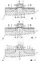
图1为与根据本发明的半导体器件的厚度方向垂直的概略剖视图。图2为与已知半导体器件的厚度方向垂直的概略剖视图。这两种器件10包括半导体主体1,其在这种情况下包含在图中并未分离地示出的硅半导体衬底。器件10实际上包括位于边缘处的隔离区(未示出),例如所谓的沟槽或LOCOS(=硅的局部氧化)隔离。实际上,半导体主体1通常还包括n型以及p型区域以用于既形成NMOS又形成PMOS晶体管,此处只示出了其中一个。在半导体主体1的表面处,存在源区2和漏区3及介于它们之间的通道区4,在这种情况下源区2和漏区3为n型,而通道区4为p型,通道区4上方存在电介质区5,在这种情况下电介质区5为氮氧化硅。源区2和漏区3分别连接至源区延伸部分2A和漏区延伸部分3A上,它们位于垫片7下方,垫片7在这种情况下为二氧化硅,其毗邻栅电极6,栅电极6在这种情况下为多晶硅。源区2和漏区3的厚度和掺杂浓度处于分别介于40和70nm以及1021和5×10²¹at/cm3之间的范围内。对于这些区2、3的延伸部分2A、3A,所述值分别为10至30nm以及1020和1021at/cm3。在这种情况下,栅电极的宽度介于10和100nm之间,而厚度介于50和150nm之间,而垫片7的宽度例如处于40至120nm的范围内。源区2和漏区3被连接区2B、3B覆盖,连接区2B、3B包含金属硅化物,在这种情况下为厚度处于25至35nm范围内的钴二硅化物。栅电极6被相同材料的连接区6B覆盖。1 is a schematic cross-sectional view perpendicular to the thickness direction of a semiconductor device according to the present invention. 2 is a schematic cross-sectional view perpendicular to the thickness direction of a known semiconductor device. Both
在已知器件10中(参见图2),在利用参考数字20表示的点处,在连接区2B、3B与衬底之间可能出现增加的泄漏电流或甚至击穿。在根据本发明的器件中(参见图1),在源区2和漏区3与相关延伸部分2A、3A之间存在中间区2C、3C,该中间区具有中间厚度和中间掺杂浓度。在这种情况下,厚度范围为从大约20至50nm而掺杂浓度范围介于1018和5×10¹⁸at/cm3之间。利用这些中间区2C、3C,在已知器件中的临界区20的位置处的泄漏电流在根据本发明的器件10中受到限制,击穿的危险也受到限制。利用这点,源区2和漏区3与衬底之间的二极管的性能就得到显著地改善,因此也显著地改善了该实例的MOSFET的性能。In the known device 10 (see FIG. 2 ), at the point indicated with the
在这个实例中,金属硅化物区2B、3B至少部分地凹进于半导体主体1中,因为它通过将金属沉积于半导体主体1的表面上而形成,该金属在热处理中与半导体主体的硅反应。在图中,区2B、3B全部凹进。实际上,硅化物区2B、3B的顶面甚至可以位于半导体主体1的表面下方。在此类器件10中,根据本发明的措施的优点相当地显著。如这个实例中的情况那样,中间区2C、3C优选地利用离子注入技术形成,并且基本上全部位于垫片7下方。这个实例的发明的器件10使用根据本发明的方法按照以下方式制造。In this example, the
图3至6为在使用根据本发明的方法的一个实施例的制造过程的连续阶段中,与半导体器件的厚度方向垂直的概略剖视图。起始步骤(参见图3)部分地为惯常步骤,在这种情况下并未分离地示出。半导体主体1的表面被电介质层5覆盖,电介质层5在这种情况下包括氮氧化硅并且厚度介于0.5与1.5nm范围内。在这种情况下为50nm厚度的多晶硅层6在这种情况下利用CVD(=化学蒸汽沉积)方法提供于其上,多晶硅层6可以或可以不经过掺杂。接着,利用光刻和蚀刻方法限定栅电极6。通过均匀地沉积电介质层而形成垫片7,该电介质层随后受到各向异性地蚀刻。接着,利用第一离子注入I1形成源区2和漏区3。在这个过程中,栅电极6并未受到屏蔽,因此栅电极的硅也经过掺杂。3 to 6 are schematic cross-sectional views perpendicular to the thickness direction of the semiconductor device at successive stages of a manufacturing process using an embodiment of the method according to the present invention. The initial steps (see FIG. 3 ) are partly conventional steps and are not shown separately in this case. The surface of the
随后(参见图4),利用第二离子注入I2形成中间区2C、3C。这种注入I2相对于法线成一定角度A进行,角度A介于0与45度范围内,在这种情况下大约相对于法线成20度。因此,中间区2C、3C形成于垫片7下方。接着,通过在处于900至1100摄氏度的温度范围内使用RTA(=快速热退火)进行热处理将注入I1和I2两者回火。Subsequently (see FIG. 4 ),
随后(参见图5),利用蚀刻除去垫片7,此后利用第三离子注入I3形成源区和漏区延伸部分2A、3A。这种注入I3随后通过热处理进行回火,例如通过所谓的闪光或激光RTA(=快速热退火)进行。Subsequently (see FIG. 5 ), the
随后(参见图6),通过蒸汽沉积提供金属层8,在这种情况下为钴。因此,在源区2和漏区3及栅电极6的位置处,在第一低温热处理中形成了反应产物即富金属的金属硅化物,掩模同时从该处除去。随后利用蚀刻除去垫片7位置处的所述区上的多余金属和全部金属层8。然后,在更高温度的进一步热处理中,将富钴硅化物转变成钴二硅化物,结果(参见图1)形成源区2和漏区3的连接区2B、3B以及栅电极6的连接区6B。Subsequently (see FIG. 6 ), a
最后,按照惯常方式完成晶体管T的制造。就是说,应用了一个或多个电介质层并且其带有接触开口,此后应用导电层例如铝导电层并且为其形成图案,然后从所述导电层形成源区2和漏区3以及栅电极6所用的连接导体。为了简化起见,这些步骤并未示于图中。利用分离技术例如锯切获得各个独立的器件10。Finally, the fabrication of transistor T is completed in a conventional manner. That is, one or more dielectric layers are applied and have contact openings, after which a conductive layer, such as an aluminum conductive layer, is applied and patterned, and the
本发明并不限于此处所述的实施例的实例,并且在本发明的范围内,本发明所属领域的普通技术人员可以做出许多变型和改动。例如,可以制造具有不同的几何和/或不同的尺寸的器件。可以使用玻璃、陶瓷或合成树脂衬底,而非硅衬底。半导体主体于是可通过所谓的SOI(=绝缘体上的硅)形成。为此目的,可以或可以不使用所谓的衬底迁移技术。The present invention is not limited to the examples of embodiment described herein, and within the scope of the present invention, many variations and modifications may be made by those skilled in the art to which the present invention pertains. For example, devices can be fabricated with different geometries and/or different dimensions. A glass, ceramic, or synthetic resin substrate may be used instead of a silicon substrate. The semiconductor body can then be formed by so-called SOI (=silicon on insulator). For this purpose, so-called substrate transfer techniques may or may not be used.
还应当指出,在本发明的范围内,可以使用除了实例中所述以外的材料。例如,可以使用其它金属如镍或钛,而非钴。可以有利地使用金属栅电极,而非包含硅的栅电极。所述材料或其它材料还可以使用不同的沉积技术,如外延生长、CVD、溅射和蒸汽沉积。可以使用“烘干”技术如等离子体蚀刻,而非湿化学蚀刻,反之也可。还应当指出,器件可包括其它有源和无源半导体元件或电子部件,而不管是否呈集成电路的形式。It should also be noted that materials other than those described in the examples may be used within the scope of the invention. For example, other metals such as nickel or titanium may be used instead of cobalt. Metal gate electrodes may advantageously be used instead of gate electrodes comprising silicon. Said or other materials may also be deposited using different deposition techniques, such as epitaxial growth, CVD, sputtering and vapor deposition. "Drying" techniques such as plasma etching can be used instead of wet chemical etching, and vice versa. It should also be noted that a device may include other active and passive semiconductor elements or electronic components, whether in the form of integrated circuits or not.
Claims (7)
Applications Claiming Priority (3)
| Application Number | Priority Date | Filing Date | Title |
|---|---|---|---|
| EP03103857.3 | 2003-10-17 | ||
| EP03103857 | 2003-10-17 | ||
| PCT/IB2004/052021WO2005038900A1 (en) | 2003-10-17 | 2004-10-07 | Semiconductor device and method of manufacturing such a semiconductor device |
Publications (2)
| Publication Number | Publication Date |
|---|---|
| CN1868046A CN1868046A (en) | 2006-11-22 |
| CN1868046Btrue CN1868046B (en) | 2011-12-28 |
Family
ID=34443036
Family Applications (1)
| Application Number | Title | Priority Date | Filing Date |
|---|---|---|---|
| CN2004800304247AExpired - LifetimeCN1868046B (en) | 2003-10-17 | 2004-10-07 | Semiconductor device and method of manufacturing such a semiconductor device |
Country Status (5)
| Country | Link |
|---|---|
| US (1) | US20070082450A1 (en) |
| EP (1) | EP1678750A1 (en) |
| JP (1) | JP2007508705A (en) |
| CN (1) | CN1868046B (en) |
| WO (1) | WO2005038900A1 (en) |
Cited By (1)
| Publication number | Priority date | Publication date | Assignee | Title |
|---|---|---|---|---|
| KR101753076B1 (en) | 2010-02-08 | 2017-07-03 | 세미컨덕터 콤포넨츠 인더스트리즈 엘엘씨 | Electronic device including doped regions between channel and drain regions and a process of forming the same |
Families Citing this family (5)
| Publication number | Priority date | Publication date | Assignee | Title |
|---|---|---|---|---|
| KR100653995B1 (en) | 2005-03-17 | 2006-12-05 | 주식회사 하이닉스반도체 | Local implant method for semiconductor device manufacturing |
| CN102110717B (en)* | 2011-01-26 | 2013-01-02 | 成都瑞芯电子有限公司 | Trench metal oxide semiconductor field effect transistor and manufacturing method thereof |
| CN103579078A (en)* | 2012-07-31 | 2014-02-12 | 上海华虹Nec电子有限公司 | Method for restraining reverse narrow channel effect in shallow trench isolation technology |
| US9640645B2 (en)* | 2013-09-05 | 2017-05-02 | Taiwan Semiconductor Manufacturing Company Limited | Semiconductor device with silicide |
| CN108962979B (en)* | 2018-09-12 | 2024-01-02 | 长江存储科技有限责任公司 | High voltage device and semiconductor device |
Citations (8)
| Publication number | Priority date | Publication date | Assignee | Title |
|---|---|---|---|---|
| US4818715A (en)* | 1987-07-09 | 1989-04-04 | Industrial Technology Research Institute | Method of fabricating a LDDFET with self-aligned silicide |
| US5015598A (en)* | 1989-11-03 | 1991-05-14 | U.S. Philips Corporation | Method of manufacturing a device comprising MIS transistors having a gate electrode in the form of an inverted "T" |
| EP0506427A1 (en)* | 1991-03-27 | 1992-09-30 | STMicroelectronics, Inc. | An integrated gate field-effect transistor with gate-drain overlap and method of making the same |
| US5747373A (en)* | 1996-09-24 | 1998-05-05 | Taiwan Semiconductor Manufacturing Company Ltd. | Nitride-oxide sidewall spacer for salicide formation |
| US6083846A (en)* | 1997-01-10 | 2000-07-04 | Advanced Micro Devices, Inc. | Graded MOS transistor junction formed by aligning a sequence of implants to a selectively removable polysilicon sidewall space and oxide thermally grown thereon |
| US6187620B1 (en)* | 1996-12-06 | 2001-02-13 | Advanced Micro Devices, Inc. | Integrated circuit having sacrificial spacers for producing graded NMOS source/drain junctions possibly dissimilar from PMOS source/drain junctions |
| US6284630B1 (en)* | 1999-10-20 | 2001-09-04 | Advanced Micro Devices, Inc. | Method for fabrication of abrupt drain and source extensions for a field effect transistor |
| US6380053B1 (en)* | 1999-08-30 | 2002-04-30 | Sony Corporation | Method for producing a semiconductor device with an accurately controlled impurity concentration profile in the extension regions |
Family Cites Families (6)
| Publication number | Priority date | Publication date | Assignee | Title |
|---|---|---|---|---|
| US5686324A (en)* | 1996-03-28 | 1997-11-11 | Mosel Vitelic, Inc. | Process for forming LDD CMOS using large-tilt-angle ion implantation |
| US5913124A (en)* | 1997-05-24 | 1999-06-15 | United Microelectronics Corporation | Method of making a self-aligned silicide |
| US5970353A (en)* | 1998-03-30 | 1999-10-19 | Advanced Micro Devices, Inc. | Reduced channel length lightly doped drain transistor using a sub-amorphous large tilt angle implant to provide enhanced lateral diffusion |
| US6225176B1 (en)* | 1999-02-22 | 2001-05-01 | Advanced Micro Devices, Inc. | Step drain and source junction formation |
| KR100327347B1 (en)* | 2000-07-22 | 2002-03-06 | Samsung Electronics Co Ltd | Metal oxide semiconductor field effect transistor having reduced resistance between source and drain and fabricating method thereof |
| US6406964B1 (en)* | 2000-11-01 | 2002-06-18 | Advanced Micro Devices, Inc. | Method of controlling junction recesses in a semiconductor device |
- 2004
- 2004-10-07JPJP2006534878Apatent/JP2007508705A/ennot_activeWithdrawn
- 2004-10-07CNCN2004800304247Apatent/CN1868046B/ennot_activeExpired - Lifetime
- 2004-10-07EPEP04770207Apatent/EP1678750A1/ennot_activeWithdrawn
- 2004-10-07USUS10/575,288patent/US20070082450A1/ennot_activeAbandoned
- 2004-10-07WOPCT/IB2004/052021patent/WO2005038900A1/enactiveApplication Filing
Patent Citations (8)
| Publication number | Priority date | Publication date | Assignee | Title |
|---|---|---|---|---|
| US4818715A (en)* | 1987-07-09 | 1989-04-04 | Industrial Technology Research Institute | Method of fabricating a LDDFET with self-aligned silicide |
| US5015598A (en)* | 1989-11-03 | 1991-05-14 | U.S. Philips Corporation | Method of manufacturing a device comprising MIS transistors having a gate electrode in the form of an inverted "T" |
| EP0506427A1 (en)* | 1991-03-27 | 1992-09-30 | STMicroelectronics, Inc. | An integrated gate field-effect transistor with gate-drain overlap and method of making the same |
| US5747373A (en)* | 1996-09-24 | 1998-05-05 | Taiwan Semiconductor Manufacturing Company Ltd. | Nitride-oxide sidewall spacer for salicide formation |
| US6187620B1 (en)* | 1996-12-06 | 2001-02-13 | Advanced Micro Devices, Inc. | Integrated circuit having sacrificial spacers for producing graded NMOS source/drain junctions possibly dissimilar from PMOS source/drain junctions |
| US6083846A (en)* | 1997-01-10 | 2000-07-04 | Advanced Micro Devices, Inc. | Graded MOS transistor junction formed by aligning a sequence of implants to a selectively removable polysilicon sidewall space and oxide thermally grown thereon |
| US6380053B1 (en)* | 1999-08-30 | 2002-04-30 | Sony Corporation | Method for producing a semiconductor device with an accurately controlled impurity concentration profile in the extension regions |
| US6284630B1 (en)* | 1999-10-20 | 2001-09-04 | Advanced Micro Devices, Inc. | Method for fabrication of abrupt drain and source extensions for a field effect transistor |
Non-Patent Citations (1)
| Title |
|---|
| 同上. |
Cited By (1)
| Publication number | Priority date | Publication date | Assignee | Title |
|---|---|---|---|---|
| KR101753076B1 (en) | 2010-02-08 | 2017-07-03 | 세미컨덕터 콤포넨츠 인더스트리즈 엘엘씨 | Electronic device including doped regions between channel and drain regions and a process of forming the same |
Also Published As
| Publication number | Publication date |
|---|---|
| CN1868046A (en) | 2006-11-22 |
| US20070082450A1 (en) | 2007-04-12 |
| WO2005038900A1 (en) | 2005-04-28 |
| JP2007508705A (en) | 2007-04-05 |
| EP1678750A1 (en) | 2006-07-12 |
Similar Documents
| Publication | Publication Date | Title |
|---|---|---|
| CN100562988C (en) | Method of fabricating semiconductor-on-insulator device | |
| CN101300677B (en) | Electrically programmable fuse and method of making same | |
| KR101113009B1 (en) | Method and apparatus for forming an ??? body-contacted transistor | |
| US6858506B2 (en) | Method for fabricating locally strained channel | |
| US6784035B2 (en) | Field effect transistor having source and/or drain forming Schottky or Schottky-like contact with strained semiconductor substrate | |
| US9178061B2 (en) | Method for fabricating MOSFET on silicon-on-insulator with internal body contact | |
| US20100032754A1 (en) | Semiconductor device and method of manufacturing the semiconductor device | |
| US20050118793A1 (en) | Schottky-barrier MOSFET manufacturing method using isotropic etch process | |
| JP4450267B2 (en) | SOI-MOS Field Effect Transistor Manufacturing Method | |
| US6096591A (en) | Method of making an IGFET and a protected resistor with reduced processing steps | |
| US20070194353A1 (en) | Metal source/drain Schottky barrier silicon-on-nothing MOSFET device and method thereof | |
| US5804856A (en) | Depleted sidewall-poly LDD transistor | |
| US5824588A (en) | Double spacer salicide MOS process and device | |
| US7208383B1 (en) | Method of manufacturing a semiconductor component | |
| KR100574172B1 (en) | Manufacturing method of semiconductor device | |
| CN1868046B (en) | Semiconductor device and method of manufacturing such a semiconductor device | |
| KR100658088B1 (en) | Low leakage mos transistor | |
| US20050098818A1 (en) | Drain/source extension structure of a field effect transistor including doped high-k sidewall spacers | |
| US6281086B1 (en) | Semiconductor device having a low resistance gate conductor and method of fabrication the same | |
| US6312999B1 (en) | Method for forming PLDD structure with minimized lateral dopant diffusion | |
| US6638829B1 (en) | Semiconductor structure having a metal gate electrode and elevated salicided source/drain regions and a method for manufacture | |
| JP3161379B2 (en) | Semiconductor device and method of manufacturing semiconductor device | |
| JPH11111979A (en) | Semiconductor device and its manufacture | |
| US20050170620A1 (en) | Transistors for semiconductor device and methods of fabricating the same | |
| KR100898257B1 (en) | Manufacturing method of semiconductor device |
Legal Events
| Date | Code | Title | Description |
|---|---|---|---|
| C06 | Publication | ||
| PB01 | Publication | ||
| C10 | Entry into substantive examination | ||
| SE01 | Entry into force of request for substantive examination | ||
| ASS | Succession or assignment of patent right | Owner name:NXP CO., LTD. Free format text:FORMER OWNER: KONINKLIJKE PHILIPS ELECTRONICS N.V. Effective date:20071012 | |
| C41 | Transfer of patent application or patent right or utility model | ||
| TA01 | Transfer of patent application right | Effective date of registration:20071012 Address after:Holland Ian Deho Finn Applicant after:NXP B.V. Address before:Holland Ian Deho Finn Applicant before:Koninklijke Philips Electronics N.V. | |
| C14 | Grant of patent or utility model | ||
| GR01 | Patent grant | ||
| ASS | Succession or assignment of patent right | Owner name:IMEC CORP. Free format text:FORMER OWNER: KONINKL PHILIPS ELECTRONICS NV Effective date:20120326 | |
| C41 | Transfer of patent application or patent right or utility model | ||
| TR01 | Transfer of patent right | Effective date of registration:20120326 Address after:Leuven Patentee after:IMEC Corp. Address before:Holland Ian Deho Finn Patentee before:NXP B.V. | |
| CX01 | Expiry of patent term | Granted publication date:20111228 | |
| CX01 | Expiry of patent term |