CN1856839A - Nonvolatile semiconductor memory device using some memory blocks in multi-ary memory as binary memory blocks - Google Patents
Nonvolatile semiconductor memory device using some memory blocks in multi-ary memory as binary memory blocksDownload PDFInfo
- Publication number
- CN1856839A CN1856839ACNA2004800273713ACN200480027371ACN1856839ACN 1856839 ACN1856839 ACN 1856839ACN A2004800273713 ACNA2004800273713 ACN A2004800273713ACN 200480027371 ACN200480027371 ACN 200480027371ACN 1856839 ACN1856839 ACN 1856839A
- Authority
- CN
- China
- Prior art keywords
- data
- order
- write
- memory
- erasing
- Prior art date
- Legal status (The legal status is an assumption and is not a legal conclusion. Google has not performed a legal analysis and makes no representation as to the accuracy of the status listed.)
- Granted
Links
Images


Classifications
- G—PHYSICS
- G11—INFORMATION STORAGE
- G11C—STATIC STORES
- G11C16/00—Erasable programmable read-only memories
- G11C16/02—Erasable programmable read-only memories electrically programmable
- G11C16/06—Auxiliary circuits, e.g. for writing into memory
- G11C16/10—Programming or data input circuits
- G—PHYSICS
- G11—INFORMATION STORAGE
- G11C—STATIC STORES
- G11C11/00—Digital stores characterised by the use of particular electric or magnetic storage elements; Storage elements therefor
- G11C11/56—Digital stores characterised by the use of particular electric or magnetic storage elements; Storage elements therefor using storage elements with more than two stable states represented by steps, e.g. of voltage, current, phase, frequency
- G11C11/5621—Digital stores characterised by the use of particular electric or magnetic storage elements; Storage elements therefor using storage elements with more than two stable states represented by steps, e.g. of voltage, current, phase, frequency using charge storage in a floating gate
- G11C11/5628—Programming or writing circuits; Data input circuits
- G11C11/5635—Erasing circuits
- G—PHYSICS
- G11—INFORMATION STORAGE
- G11C—STATIC STORES
- G11C16/00—Erasable programmable read-only memories
- G11C16/02—Erasable programmable read-only memories electrically programmable
- G11C16/06—Auxiliary circuits, e.g. for writing into memory
- G11C16/10—Programming or data input circuits
- G11C16/14—Circuits for erasing electrically, e.g. erase voltage switching circuits
- G11C16/16—Circuits for erasing electrically, e.g. erase voltage switching circuits for erasing blocks, e.g. arrays, words, groups
- G—PHYSICS
- G11—INFORMATION STORAGE
- G11C—STATIC STORES
- G11C2211/00—Indexing scheme relating to digital stores characterized by the use of particular electric or magnetic storage elements; Storage elements therefor
- G11C2211/56—Indexing scheme relating to G11C11/56 and sub-groups for features not covered by these groups
- G11C2211/564—Miscellaneous aspects
- G11C2211/5641—Multilevel memory having cells with different number of storage levels
Landscapes
- Engineering & Computer Science (AREA)
- Computer Hardware Design (AREA)
- Read Only Memory (AREA)
Abstract
Description
Translated fromChinese(对相关申请的交叉引用)(cross-reference to related application)
本申请基于在2003年9月29日提交的在先的日本专利申请No.2003-338545,并要求其作为优先权,在此引用其全部内容作为参考。This application is based on and claims priority from prior Japanese Patent Application No. 2003-338545 filed on September 29, 2003, the entire contents of which are incorporated herein by reference.
技术领域technical field
本发明涉及可电改写的非易失性半导体存储器件,更具体而言,涉及选择性地使用存储多进制(multilevel,又称“多值”)信息的存储单元阵列中的一些存储块作为存储二进制信息(又称“二值信息”)的存储块的快擦写存储器(又称闪存)。The present invention relates to an electrically rewritable non-volatile semiconductor storage device, and more specifically, relates to selectively using some memory blocks in a memory cell array storing multilevel (multilevel, also known as "multi-value") information as Flash memory (also known as flash memory) that stores memory blocks of binary information (also known as "binary information").
背景技术Background technique
在许多存储系统中,文件分配表(FAT)是必需的。FAT是存储各种文件的位置的块。每当对存储系统执行写入或擦除时,必须将FAT改写。为此,在写入FAT的区域中,写入速度必须尽可能高。In many storage systems, a file allocation table (FAT) is required. FAT is a block that stores the location of various files. Whenever writing or erasing is performed on the storage system, the FAT must be rewritten. For this reason, in the area where FAT is written, the writing speed must be as high as possible.
在当前的快擦写存储器中,在一个单元中存储1位信息的通常的存储单元(二进制技术)和使用可在一个单元中存储2位信息(或三个或更多个位的信息)的多进制技术的存储单元是公知的。In current flash memory, the usual memory cell (binary technology) that stores 1 bit of information in one cell and the memory cell using memory that can store 2 bits of information (or three or more bits of information) in one cell Storage units of multi-ary technology are known.
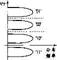
在使用多进制技术的存储单元中,例如,如图1所示,在四个步骤中改变存储单元的阈值电压Vth的分布。通过使“01”、“00”、“10”和“11”与各分布对应,存储二位信息。当使用该多进制技术时,与二进制技术相比,存储容量可以翻倍。In a memory cell using the multi-ary technique, for example, as shown in FIG. 1, the distribution of the threshold voltage Vth of the memory cell is changed in four steps. Two-bit information is stored by associating "01", "00", "10", and "11" with each distribution. When using this multi-ary technique, the storage capacity can be doubled compared to the binary technique.
在使用多进制技术的快擦写存储器中,写入速度比二进制技术低。作为针对这一点的措施,将存储单元阵列分成多个块,并且,在诸如被频繁写入访问的FAT的块中,不使用多进制技术,即,如图2所示,为了增加写入速度,选择性地执行使用二进制技术的写入。采用这种配置,在由多进制技术块保证存储容量的同时通过二进制技术块实施高速写入。In flash memories using multi-ary technology, the writing speed is lower than binary technology. As a measure against this, the memory cell array is divided into multiple blocks, and, in blocks such as FAT which are frequently write-accessed, the multi-ary technique is not used, that is, as shown in FIG. speed, selectively performing writes using binary techniques. With this configuration, high-speed writing is implemented by binary technology blocks while securing storage capacity by multi-binary technology blocks.
NAND快擦写存储器对二进制技术和多进制技术使用不同的写入方法。二进制技术使用自升压(SB,self-boost)方法。多进制技术使用被擦除区域自升压(EASB)方法。在两种方法中,以相同的方式执行“0”写入。向被选择的字线(被选择的单元晶体管的控制栅CG)施加写入电压Vpgm(例如,20V)。向未被选择的字线施加中间电压Vpass(例如,10V)。将位线BL设为0V,将位线侧的选择晶体管SGD的栅设为电源电压Vdd,以将选择晶体管SGD设为导电状态。因此,电子被注入到被选择的单元晶体管的浮置栅中,以增加阈值电压。NAND flash memory uses different writing methods for binary and multi-binary techniques. Binary technology uses a self-boost (SB, self-boost) approach. Multi-ary technology uses the erased area self-boosting (EASB) method. In both methods, "0" writing is performed in the same manner. A write voltage Vpgm (for example, 20V) is applied to the selected word line (control gate CG of the selected cell transistor). An intermediate voltage Vpass (for example, 10V) is applied to the unselected word lines. The bit line BL is set to 0 V, and the gate of the selection transistor SGD on the bit line side is set to the power supply voltage Vdd to bring the selection transistor SGD into a conductive state. Accordingly, electrons are injected into the floating gate of the selected cell transistor to increase the threshold voltage.
相反,执行“1”写入(非写入)的方式在SB方法和EASB方法之间改变。在SB方法中,如图3所示,向被选择的字线施加写入电压Vpgm(20V)。向未被选择的字线施加中间电压Vpass(10V)。将位线BL设为电源电压Vdd,并将位线侧的选择晶体管SGD的栅设为电源电压Vdd,以将选择晶体管SGD设为非导电状态。另外,将共用源线侧的选择晶体管SGS的栅设为0V,以将选择晶体管SGS也设为非导电状态。由此,没有电子被注入到被选择的单元晶体管的浮置栅中,使得阈值电压保持擦除状态。如上所述,在SB方法中,在将串联在选择晶体管SGD和SGS之间的单元晶体管设为导电状态的同时执行对于被选择的单元晶体管的写入。On the contrary, the way of performing "1" writing (non-writing) is changed between the SB method and the EASB method. In the SB method, as shown in FIG. 3, a write voltage Vpgm (20V) is applied to a selected word line. An intermediate voltage Vpass (10V) is applied to unselected word lines. The bit line BL is set to the power supply voltage Vdd, and the gate of the selection transistor SGD on the bit line side is set to the power supply voltage Vdd to put the selection transistor SGD in a non-conductive state. In addition, the gate of the selection transistor SGS on the side of the common source line is set to 0V so that the selection transistor SGS is also in a non-conductive state. Thus, no electrons are injected into the floating gate of the selected cell transistor, so that the threshold voltage remains in the erased state. As described above, in the SB method, writing to a selected cell transistor is performed while setting the cell transistor connected in series between the selection transistors SGD and SGS to a conductive state.
另一方面,在EASB方法中,如图4所示,向被选择的字线施加写入电压Vpgm(20V),以将邻近被选择的字线的源线侧的字线设为0V。向其它未被选择的字线施加中间电压Vpass(10V)。将位线BL设为电源电压Vdd,并将位线侧的选择晶体管SGD的栅设为电源电压Vdd,以将选择晶体管SGD设为非导电状态。另外,将共用源线侧的选择晶体管SGS的栅设为0V,以将选择晶体管SGS也设为非导电状态。由此,没有电子被注入到被选择的单元晶体管的浮置栅中,使得阈值电压保持擦除状态。如上所述,在EASB方法中,在将被选择的单元晶体管的位线侧的单元晶体管设为导电状态、将邻近被选择的单元晶体管的源线侧的单元晶体管设为非导电状态的同时、执行对于被选择的单元晶体管的写入。在使用多进制技术的写入中,为了减少写入错误,这种方法是必需的。On the other hand, in the EASB method, as shown in FIG. 4, the write voltage Vpgm (20V) is applied to the selected word line to set the word line on the source line side adjacent to the selected word line to 0V. The intermediate voltage Vpass (10V) is applied to other unselected word lines. The bit line BL is set to the power supply voltage Vdd, and the gate of the selection transistor SGD on the bit line side is set to the power supply voltage Vdd to put the selection transistor SGD in a non-conductive state. In addition, the gate of the selection transistor SGS on the side of the common source line is set to 0V so that the selection transistor SGS is also in a non-conductive state. Thus, no electrons are injected into the floating gate of the selected cell transistor, so that the threshold voltage remains in the erased state. As described above, in the EASB method, while setting the cell transistor on the bit line side of the selected cell transistor into a conductive state, and setting the cell transistors adjacent to the selected cell transistor on the source line side into a non-conductive state, Writing to the selected cell transistor is performed. This method is necessary in order to reduce write errors in writing using multi-ary techniques.
必须将单元晶体管设为当控制栅电压为0V时被截止的阈值电压。出于这种原因,擦除方法也改变。要通过EASB方法执行写入,单元晶体管的阈值电压必须不能太低。由此,如图5所示,必须执行操作(软程序),以将通过擦除被分布为双点划线表示的那样的阈值电压Vth写回到由实线表示的一定电平。The cell transistor must be set to a threshold voltage that is turned off when the control gate voltage is 0V. For this reason, the erasing method is also changed. To perform writing by the EASB method, the threshold voltage of the cell transistor must not be too low. Thus, as shown in FIG. 5 , it is necessary to perform an operation (soft program) to write back the threshold voltage Vth distributed as indicated by a two-dot chain line by erasing back to a certain level indicated by a solid line.
如上所述,二进制技术和多进制技术使用不同的写入和擦除方法。如果要一个存储单元阵列同时包括二进制技术块和多进制技术块,那么必须在擦除后区别二进制块和多进制块。As mentioned above, binary and multi-binary techniques use different methods of writing and erasing. If a memory cell array is required to include binary technology blocks and multi-ary technology blocks at the same time, it is necessary to distinguish binary blocks and multi-ary technology blocks after erasing.
例如,日本专利申请特开公报No.2001-210082公开了一种非易失性半导体存储器件和数据存储系统,其中,在存储单元阵列中分开地形成二进制存储单元区和多进制存储单元区。在写入数据的过程中,对各字线写入识别二进制区或多进制区的标记数据。当读出标记数据时,可以识别二进制页面而或多进制页面,使得可以执行与二进制技术或多进制技术对应的写入或读取。但是,在该现有技术公开的技术中,二进制存储单元区和多进制存储单元区是事先分开地形成的。因此,用户的选择自由度较低。For example, Japanese Patent Application Laid-Open Publication No. 2001-210082 discloses a nonvolatile semiconductor memory device and a data storage system in which a binary memory cell area and a multi-binary memory cell area are separately formed in a memory cell array . In the process of writing data, mark data identifying a binary area or a multi-ary area is written to each word line. When the tag data is read out, a binary page or a multi-binary page can be identified, so that writing or reading corresponding to the binary technique or the multi-binary technique can be performed. However, in the technique disclosed in this prior art, the binary storage cell area and the multi-binary storage cell area are separately formed in advance. Therefore, the user's degree of freedom of choice is low.
日本专利申请特开公报No.2001-006374公开了选择性地以二进制模式或多进制模式操作的半导体存储器件和系统。在该现有技术公开的技术中,为了对各字线选择性地使用存储区作为二进制区或多进制区,准备二进制/多进制管理表,以表示将存储区指定为二进制区或多进制区。用户可以自由地以二进制模式或多进制模式操作器件。但是,为了区分二进制块和多进制块,必需有专用的硬件,从而导致芯片尺寸增加。Japanese Patent Application Laid-Open Publication No. 2001-006374 discloses a semiconductor memory device and system selectively operating in a binary mode or a multi-binary mode. In the technique disclosed in this prior art, in order to selectively use a storage area as a binary area or a multi-binary area for each word line, a binary/multi-binary management table is prepared to indicate that the storage area is designated as a binary area or a multi-binary area. Binary area. Users are free to operate the device in binary mode or multi-binary mode. However, in order to distinguish binary blocks from multi-binary blocks, dedicated hardware is necessary, resulting in an increase in chip size.
如上所述,对于常规的非易失性半导体存储器件,如果要以二进制模式或多进制模式选择性地操作存储单元阵列中的各个块,那么用户的选择自由度变低。如果要增加块选择的自由度,就必需有专用的硬件,从而导致芯片尺寸增加。As described above, with a conventional nonvolatile semiconductor memory device, if each block in a memory cell array is to be selectively operated in a binary mode or a multi-binary mode, the user's degree of freedom of choice becomes low. If the degree of freedom of block selection is to be increased, dedicated hardware is necessary, resulting in an increase in chip size.
发明内容Contents of the invention
根据本发明的一个方面,提供一种非易失性半导体存储器件,包括:由具有可电改写的非易失性半导体存储单元的多个存储块构成的存储单元阵列;与外部器件通信的接口;和根据输入到接口的数据写入命令、用第一写入次序或第二写入次序将数据写入存储单元阵列中的写入电路,在从接口输入根据第一写入次序的数据写入命令时,写入电路在要被写入命令写入访问的块中的存储单元中写入的标记数据具有第一值时执行写入命令,并在标记数据具有第二值时不执行写入命令。According to one aspect of the present invention, there is provided a nonvolatile semiconductor memory device, comprising: a memory cell array composed of a plurality of memory blocks having electrically rewritable nonvolatile semiconductor memory cells; an interface for communicating with external devices and according to the data write command input to the interface, with the first write order or the second write order data is written into the write circuit in the memory cell array, and the data write according to the first write order is input from the interface When the command is input, the write circuit executes the write command when the flag data written in the memory cell in the block to be written into by the write command has a first value, and does not execute the write command when the flag data has a second value. Enter command.
根据本发明的另一方面,提供一种非易失性半导体存储器件,包括:由具有可电改写的非易失性半导体存储单元的多个存储块构成的存储单元阵列;与外部器件通信的接口;根据输入到接口的数据擦除命令、用第一擦除次序或第二擦除次序对各存储块擦除存储单元中的数据的擦除电路,当从接口输入根据第一擦除次序的数据擦除命令时,擦除电路通过使用第一擦除次序执行被选择的存储块中的存储单元的擦除,并将标记数据写入被擦除的存储块中的一些存储单元中;和根据输入到接口的数据写入命令、在通过使用第一擦除次序执行擦除时根据第一写入次序、或在通过使用第二擦除次序执行擦除时根据第二写入次序将数据写入各存储块的各页面中的写入电路,当从接口输入根据第一写入次序的数据写入命令时,写入电路在要被写入命令写入访问的块中的一些存储单元中写入的标记数据具有第一值时执行写入命令,并在标记数据具有第二值时不执行写入命令。According to another aspect of the present invention, there is provided a nonvolatile semiconductor memory device, comprising: a memory cell array composed of a plurality of memory blocks having electrically rewritable nonvolatile semiconductor memory cells; Interface; according to the data erasing command input to the interface, use the first erasing order or the second erasing order to erase the data in the storage unit of each memory block, when the interface is input according to the first erasing order During the data erasing command, the erasing circuit executes the erasing of the memory cells in the selected memory block by using the first erasing sequence, and writes the mark data into some memory cells in the erased memory block; and according to a data write command input to the interface, according to the first write order when erasing is performed by using the first erase order, or according to the second write order when erasing is performed by using the second erase order Data is written into a write circuit in each page of each memory block, when a data write command according to the first write order is input from the interface, the write circuit writes some memory in the block to be written into by the write command The write command is executed when the flag data written in the cell has a first value, and the write command is not executed when the flag data has a second value.
附图说明Description of drawings
图1是表示使用多进制技术的存储单元的阈值电压分布的示图;FIG. 1 is a diagram representing threshold voltage distributions of memory cells using multi-ary technology;
图2是用于解释使用多进制技术和二进制技术的常规的非易失性半导体存储器件的框图;2 is a block diagram for explaining a conventional nonvolatile semiconductor memory device using a multi-ary technique and a binary technique;
图3是用于解释通过SB方法进行的写入操作的剖面图;3 is a cross-sectional view for explaining a write operation by the SB method;
图4是用于解释通过EASB方法进行的写入操作的剖面图;FIG. 4 is a cross-sectional view for explaining a write operation by the EASB method;
图5是用于解释为了通过EASB方法执行写入的擦除操作的示图;FIG. 5 is a diagram for explaining an erase operation for performing writing by the EASB method;
图6是表示快擦写存储器的配置的框图,以解释根据本发明的实施方式的非易失性半导体存储器件;6 is a block diagram showing a configuration of a flash memory to explain a nonvolatile semiconductor memory device according to an embodiment of the present invention;
图7是表示图6中所示的存储单元阵列的结构的电路图;FIG. 7 is a circuit diagram showing the structure of the memory cell array shown in FIG. 6;
图8是表示图7中所示的各存储块的结构的示意图;Fig. 8 is a schematic diagram showing the structure of each storage block shown in Fig. 7;
图9A是表示二进制模式中的擦除次序的流程图;Figure 9A is a flow chart representing the erase sequence in binary mode;
图9B是表示多进制模式中的擦除次序的流程图;Figure 9B is a flow chart representing the erase sequence in multi-ary mode;
图10A是表示二进制模式中的写入次序的流程图;FIG. 10A is a flow chart representing the write sequence in binary mode;
图10B是表示多进制模式中的写入次序的流程图;Fig. 10B is a flowchart showing the write sequence in multi-ary mode;
图11是表示用于将二进制标记数据读出到外部器件中的次序的流程图;Fig. 11 is a flowchart showing the sequence for reading out binary tag data into an external device;
图12A是表示二进制模式中的其它写入次序的流程图;Figure 12A is a flow chart representing other write sequences in binary mode;
图12B是表示多进制模式中的其它写入次序的流程图。Fig. 12B is a flowchart showing other write procedures in multi-ary mode.
具体实施方式Detailed ways
图6~8是用于解释根据本发明的实施方式的非易失性半导体存储器件的示图。图6是表示快擦写存储器的配置的框图。图7是表示图6中所示的存储单元阵列的结构的电路图。图8是表示图7中所示的各存储块的结构的示意图。示出NAND快擦写存储器作为例子,并示出与二进制模式和多进制模式之间的切换有关的主要部分。6 to 8 are views for explaining a nonvolatile semiconductor memory device according to an embodiment of the present invention. FIG. 6 is a block diagram showing the configuration of the flash memory. FIG. 7 is a circuit diagram showing the structure of the memory cell array shown in FIG. 6 . FIG. 8 is a schematic diagram showing the configuration of each memory block shown in FIG. 7 . A NAND flash memory is shown as an example, and main parts related to switching between binary mode and multi-binary mode are shown.
通过将快速存储单元排列为矩阵构成存储单元阵列1。列控制电路2被配置为邻近存储单元阵列1。列控制电路2控制存储单元阵列1的位线,以对存储单元执行数据擦除、数据写入或数据读取。行控制电路3被配置为选择存储单元阵列1的字线并向字线施加擦除、写入或读取所需的电压。另外,配置控制存储单元阵列1的源线的源线控制电路4和控制其中形成存储单元阵列1的p阱的p阱控制电路5。The
数据输入/输出缓冲器6通过I/O线与外部主机(未示出)连接,以接收写入数据、输出读出数据并接收地址数据或命令数据。数据输入/输出缓冲器6向列控制电路2发送接收的写入数据,并从列控制电路2接收读出数据。另外,要选择存储单元,数据输入/输出缓冲器6通过状态机8向列控制电路2或行控制电路3发送外部地址数据。并且,数据输入/输出缓冲器6将来自主机的命令数据发送到命令接口7。The data input/
一旦接收到来自主机的控制信号,命令接口7就确定输入到数据输入/输出缓冲器6的数据是否为写入数据、命令数据或地址数据。如果该数据是命令数据,那么将其作为接收命令信号转移到状态机8。Upon receiving a control signal from the host, the
状态机8管理整个快擦写存储器。状态机8通过命令接口7接收从主机输入的命令,并管理读取、写入、擦除和数据输入/输出。
如图7所示,存储单元阵列1被分为多个(1024个)存储块BLOCK0~BLOCK1023。这些块是将在二进制模式或多进制模式中被选择性使用的最小单元。如代表性的存储块BLOCKi表示的那样,存储块BLOCK0~BLOCK1023中的每一个是由8512个NAND存储单元形成的。As shown in FIG. 7, the
在本例子中,通过串联四个存储单元(单元晶体管)M,构成各NAND存储单元。NAND存储单元的一个端子通过与选择栅线SGD连接的选择栅S与位线BL(BLe0~BLe4255和BLo0~BLo4255)连接。NAND存储单元的另一端子通过与选择栅线SGS连接的选择栅S与共用源线C源连接。各存储单元M的控制栅与字线WL(WL0_i~WL3_i)连接。对从0计数的偶数位线BLe和奇数位线BLo互相独立地执行数据写入/读取。在与一个字线WL连接的8512个存储单元中,4256个存储单元与偶数位线BLe连接,对这4256个存储单元同时执行数据写入/读取。分别存储1位数据的4256个存储单元的数据构成称为页面(page)的单元。类似地,与奇数位线BLo连接的4256个存储单元构成另一页面。同时对该页面中的存储单元执行数据写入/读取。In this example, four memory cells (cell transistors) M are connected in series to form each NAND memory cell. One terminal of the NAND memory cell is connected to the bit lines BL (BLe0 to BLe4255 and BLo0 to BLo4255) through the selection gate S connected to the selection gate line SGD. The other terminal of the NAND memory cell is connected to the common source line C through the select gate S connected to the select gate line SGS. The control gate of each memory cell M is connected to the word line WL (WL0_i to WL3_i). Data writing/reading is performed independently of each other on the even-numbered bit line BLe and the odd-numbered bit line BLo counted from 0. Of the 8512 memory cells connected to one word line WL, 4256 memory cells are connected to the even bit line BLe, and data writing/reading is simultaneously performed on these 4256 memory cells. Data of 4256 storage cells each storing 1-bit data constitutes a unit called a page. Similarly, 4256 memory cells connected to the odd bit line BLo constitute another page. Simultaneously, data writing/reading is performed on memory cells in the page.
如图8所示,在图7中所示的各个块BLOCK中,对各个页面(存储页面0~3)执行诸如写入、读取或擦除的访问操作。例如由528字节用户区和3字节二进制标记数据区形成存储页面0~3中的每一个。As shown in FIG. 8, in each block BLOCK shown in FIG. 7, an access operation such as writing, reading, or erasing is performed on each page (
一般地,在二进制标记数据区中,存储称为热计数(hot count,HC)的数据,以对擦除的次数进行计数。将识别二进制模式或多进制模式的二进制标记数据写入热计数的一部分中。每当执行擦除时,就将数据写入热计数中,以将计数值增加“1”。要通过选择性地使用二进制技术对多进制存储器件执行写入和擦除,必须在各存储块中区分多进制模式和二进制模式。在多进制存储器件中,当一旦接收用于二进制模式操作的信号就执行擦除时,将预定的标记数据写入二进制标记数据区中的存储单元中,使得该块被识别为二进制块。要使用该块作为多进制块(MLC块),将二进制标记数据设为“1111”(即,存储单元被擦除的状态)。要使用该块作为二进制块(SLC块),写入“0000”作为二进制标记数据。读出4位二进制标记数据,并根据多数理论(又称“多值裁决理论”)将该块识别为多进制块或二进制块。Generally, in the binary mark data area, data called a hot count (HC) is stored to count the number of times of erasure. Binary tag data identifying a binary pattern or a multi-binary pattern is written into a portion of the hot count. Data is written into the hot count to increment the count value by "1" every time erasing is performed. To perform writing and erasing of a multi-binary memory device by selectively using binary technology, it is necessary to distinguish between multi-binary and binary patterns in each memory block. In a multi-binary memory device, when erasing is performed upon receiving a signal for binary mode operation, predetermined flag data is written into memory cells in a binary flag data area so that the block is recognized as a binary block. To use this block as a multi-ary block (MLC block), the binary flag data is set to "1111" (ie, the state in which the memory cell is erased). To use this block as a binary block (SLC block), write "0000" as the binary flag data. The 4-bit binary tag data is read and the block is identified as a multi-ary block or a binary block according to the majority theory (aka "multi-valued decision theory").
下面参照图9A、图9B、图10A、图10B和图11中所示的流程图说明图6~8中所示的具有上述配置的NAND快擦写存储器的操作。图9A表示二进制模式中的擦除次序。图9B表示多进制模式中的擦除次序。图10A表示二进制模式中的写入次序。图10B表示多进制模式中的写入次序。图11表示用于将二进制标记数据读出到外部器件中的次序。The operation of the NAND flash memory having the above configuration shown in FIGS. 6 to 8 will be described below with reference to the flowcharts shown in FIGS. 9A, 9B, 10A, 10B and 11. Figure 9A shows the erase order in binary mode. Figure 9B shows the erase order in multi-ary mode. Fig. 10A shows the write order in binary mode. Fig. 10B shows the write order in multi-ary mode. Fig. 11 shows the sequence for reading out binary tag data into an external device.
当要使用控制器通过软件控制操作时,在通电时间从存储单元阵列1中的存储块BLOCK0~BLOCK1023中的每一个读出二进制标记数据。存储块BLOCK0~BLOCK1023中的每一个事先被识别为要以二进制序列被访问的块或要以多进制序列被访问的块。When the operation is to be controlled by software using the controller, binary mark data is read out from each of the memory blocks BLOCK0˜BLOCK1023 in the
在识别结果的基础上,根据图9A中所示的第一次序、对要以二进制模式被写入访问的存储块执行擦除。在擦除中,首先,通过命令接口7将表示二进制存储块的命令“A2h”从主机输入到状态机8(S1)。然后,将表示第一擦除次序的擦除命令从主机输入并设置在状态机8中(S2)。接收来自主机的地址数据,并将选择要被擦除的存储块的地址设置在状态机8中(S3)。擦除要被擦除的存储块(没有软程序)(S4)。随后,将识别二进制块和HC数据的二进制标记数据写入二进制标记数据区中的存储单元中(S5)。要写入二进制标记数据,使用一般为了对擦除的次数进行计数而执行的HC数据写入序列。换句话说,当用于二进制存储块的擦除被执行时,标记被状态机8自动设置。这样,擦除操作结束(S6)。On the basis of the identification result, erasing is performed on the memory block to be write-accessed in the binary mode according to the first order shown in FIG. 9A. In erasing, first, a command "A2h" indicating a binary memory block is input from the host to the
另一方面,对于要以多进制模式被写入访问的存储块,根据图9B中所示的第二次序执行擦除。首先,通过命令接口7从主机输入擦除命令并将其设置在状态机8中(S1)。然后,从主机输入地址数据,并将用来选择要被擦除的存储块的地址设置在状态机8中(S2)。在对被选择的存储块执行擦除后,执行软程序以将阈值电压Vth设在预定的电平(S3)。随后,写入HC数据(S4),并且擦除操作结束(S5)。On the other hand, for a memory block to be write-accessed in multi-ary mode, erasure is performed according to the second order shown in FIG. 9B. First, an erase command is input from the host through the
下面将说明写入操作。在表示块应以二进制序列或多进制序列被访问的识别结果的基础上,对于已根据第一擦除次序为其执行擦除的存储块,根据图10A中所示的第一写入次序写入二进制数据。更具体地,通过命令接口7从主机输入表示二进制存储块的命令“A2h”并将其设置在状态机8中(S1)。通过命令接口7从主机输入写入命令并将其设置在状态机8中(S2)。从主机输入地址数据,并将用来选择要被写入访问的存储块的地址设置在状态机8中(S3)。对要被写入访问的存储块的每个页面设置该地址。输入并设置用于一个页面的写入数据(528字节)(S4)。然后,通过SB方法写入数据(S5)。当所有数据都被写入时,写入操作结束(S6)。如果要被写入的数据在写入结束后仍保留在存储页面0中,那么对存储页面1~3依次重复执行步骤S2~S6。在这种数据写入中,通过使用ECC技术执行错误校正。The write operation will be described below. On the basis of the recognition result indicating that the block should be accessed in binary sequence or multi-ary sequence, for the memory block for which erasure has been performed according to the first erasure order, according to the first write order shown in FIG. 10A Write binary data. More specifically, a command "A2h" representing a binary memory block is input from the host through the
对于已根据第二擦除次序为其执行擦除的存储块,根据图10B中所示的第二写入次序写入多进制数据。首先,通过命令接口7从主机输入多进制写入命令并将其设置在状态机8中(S1)。然后,从主机输入地址数据,并将用来选择要被写入访问的存储块的地址设置在状态机8中(S2)。对要被写入访问的块的每个页面设置该地址。输入并设置用于一个页面的写入数据(528字节)(S3)。然后,通过EASB方法写入数据(S4)。当所有数据都被写入时,写入操作结束(S5)。如果要被写入的数据在写入结束后仍保留在存储页面0中,那么对存储页面1~3依次重复执行步骤S1~S5。在这种数据写入中,通过使用ECC技术执行错误校正。For the memory block for which erasing has been performed according to the second erasing order, multi-ary data is written according to the second writing order shown in FIG. 10B . First, a multi-ary write command is input from the host through the
要将二进制标记数据读出到外部器件中,如图11所示,从主机输入读取命令并将其设置在状态机8中(S1)。随后,从主机将状态“74h”设置在状态机8中(S2)。因此,通过命令接口7和数据输入/输出缓冲器6输出数据(S3)。To read binary tag data into an external device, as shown in FIG. 11, a read command is input from the host and set in the state machine 8 (S1). Subsequently, the slave master sets the state "74h" in the state machine 8 (S2). Therefore, data is output through the
在以上实施方式中,在通电时间读出二进制标记数据,并使用控制器通过软件控制操作。可以通过硬件实施与上述操作相同的操作。In the above embodiments, the binary flag data is read out at power-on time, and the operation is controlled by software using the controller. The same operations as those described above can be implemented by hardware.
在这种情况下,在根据图9A或图9B中所示的第一或第二擦除次序执行擦除后,根据图12A或图12B的流程图中所示的写入次序执行写入。更具体地,对于已根据第一擦除次序为其执行擦除的存储块,根据图12A中所示的第一写入次序写入二进制数据。首先,通过命令接口7从主机输入表示二进制存储块的命令“A2h”并将其设置在状态机8中(S1)。通过命令接口7从主机输入写入命令并将其设置在状态机8中(S2)。从主机输入地址数据,并将用来选择要被写入访问的存储块的地址设置在状态机8中(S3)。为要被写入访问的存储块的每个页面设置该地址。输入并设置用于一个页面的写入数据(528字节)(S4)。然后,读出该块的二进制标记数据(S5),以确定该块是否为要以二进制序列或多进制序列被写入访问的块(S6)。当读出的二进制标记数据是“0000”时,通过SB方法写入数据(S7)。当所有数据都被写入时,写入操作结束(S8)。如果要被写入的数据在写入结束后仍保留在存储页面0中,那么对存储页面1~3依次重复执行步骤S2~S8。当读出的二进制标记数据不是“0000”时(“1111”),不执行写入命令而停止写入操作(S9)。此时,根据4位多数理论确定该块是二进制块还是多进制块。因此,可以对二进制标记数据进行错误校正。In this case, after erasing is performed in accordance with the first or second erasing order shown in FIG. 9A or 9B , writing is performed in accordance with the writing order shown in the flowchart of FIG. 12A or 12B . More specifically, for the memory block for which erasing has been performed according to the first erasing order, binary data is written according to the first writing order shown in FIG. 12A. First, a command "A2h" representing a binary memory block is input from the host through the
对于已根据第二擦除次序为其执行擦除的存储块,根据图12B中所示的第二写入次序写入多进制数据。首先,通过命令接口7从主机输入多进制写入命令并将其设置在状态机8中(S1)。然后,从主机输入地址数据,并将用来选择要被写入访问的存储块的地址设置在状态机8中(S2)。为要被写入访问的块的每个页面设置该地址。输入并设置用于一个页面的写入数据(528字节)(S3)。然后,读出该块的二进制标记数据(S4),以识别该块是否为要以二进制序列或多进制序列被写入访问的块(S5)。当读出的二进制标记数据是“1111”时,通过EASB方法写入数据(S6)。当所有数据都被写入时,写入操作结束(S7)。如果要被写入的数据在写入结束后仍保留在存储页面0中,那么对存储页面1~3依次重复执行步骤S1~S7。当读出的二进制标记数据不是“1111”时(“0000”),不执行写入命令而停止写入操作(S8)。当然,根据4位多数理论确定该块是二进制块还是多进制块。因此,可以对二进制标记数据进行错误校正。For the memory block for which erasing has been performed according to the second erasing order, multi-ary data is written according to the second writing order shown in FIG. 12B. First, a multi-ary write command is input from the host through the
根据具有上述配置的非易失性半导体存储器件,可以获得以下效果:According to the nonvolatile semiconductor memory device having the above configuration, the following effects can be obtained:
(1)在形成为多进制存储单元阵列的存储单元阵列中,可以自由选择要以二进制模式使用的块。因此,可以以较高的自由度以二进制模式或多进制模式选择性地操作存储单元阵列中的任意存储块。另外,当以二进制模式使用诸如将被频繁改写的FAT的块时,可以大大增加写入速度。(1) In a memory cell array formed as a multi-binary memory cell array, a block to be used in binary mode can be freely selected. Therefore, any memory block in the memory cell array can be selectively operated in a binary mode or a multi-binary mode with a high degree of freedom. In addition, when using blocks such as FAT that will be frequently rewritten in binary mode, the writing speed can be greatly increased.
(2)可以将二进制标记数据放在任意存储块的任意存储页面中,因此可将其放在剩余区域中的任何地方。另外,由于二进制标记数据被写入将以二进制模式使用的存储块,因此不需要专用的硬件。由此,可以在不增加芯片尺寸的情况下以二进制模式使用该块。(2) Binary tag data can be placed in any memory page of any memory block, so it can be placed anywhere in the remaining area. Also, since binary tag data is written to memory blocks to be used in binary mode, no dedicated hardware is required. Thus, the block can be used in binary mode without increasing the chip size.
(3)在使用多进制技术的擦除中,在单元的擦除后执行软程序。由于单元的阈值电压可超过0V,因此可靠性比二进制技术低。但是,在通过二进制技术进行的擦除操作中,不执行软程序。由此,可以保证较高的可靠性。(3) In erasing using the multi-ary technique, the soft program is executed after the erasing of the cell. Since the threshold voltage of the cell can exceed 0V, it is less reliable than binary technology. However, in an erase operation by binary technique, no soft program is executed. Thereby, high reliability can be ensured.
(4)对于为其设置二进制标记的存储块(将以二进制模式被访问的存储块),使用多进制技术的写入被拒绝并且不能被执行。因此,可以对存储块保证写入速度和可靠性。(4) For the memory block for which the binary flag is set (the memory block to be accessed in binary mode), writing using the multi-ary technique is rejected and cannot be performed. Therefore, writing speed and reliability can be guaranteed for the memory block.
(5)可以通过接口(数据输入/输出缓冲器6和命令接口7)将二进制标记数据输出到外部器件。由此,可以容易地从外部器件识别存储块是二进制块还是多进制块。(5) Binary tag data can be output to an external device through the interface (data input/
(6)将二进制标记数据写入各存储单元块中的多个存储单元中。当二进制标记数据被读出时,根据多数理论执行错误校正。由此,可以防止对于存储块的任何识别错误。(6) Write binary flag data into a plurality of memory cells in each memory cell block. Error correction is performed according to most theories when binary tag data is read out. Thereby, any recognition errors for memory blocks can be prevented.
如上所述,在根据本实施方式的非易失性半导体存储器件中,当在输入二进制模式命令的同时执行擦除时,将预定的标记数据写入给定存储页面的预定存储单元中,使得该块被识别为二进制模式块。多进制NAND快擦写存储器的写入时间比二进制产品的写入时间长。但是,当一些存储块被选择性地设置为二进制块、并通过SB方法被写入访问时,可以缩短对于各块的写入时间。尤其是,当将诸如被频繁改写的FAT的块设为二进制模式块时,可以增加写入速度。另外,由于二进制模式的可靠性比多进制模式的可靠性高,因此还可以保证可靠性。并且,当将标记数据写入多个存储单元中、并在读出标记数据的过程中根据多数理论执行错误校正时,可以进一步增加可靠性。由于可以将标记数据输出到外部器件,因此,可以容易地从外部器件确认设置为二进制模式的块。As described above, in the nonvolatile semiconductor memory device according to the present embodiment, when erasing is performed while a binary mode command is input, predetermined flag data is written in predetermined memory cells of a given memory page so that This block is recognized as a binary pattern block. The writing time of multi-binary NAND flash memory is longer than that of binary products. However, when some memory blocks are selectively set as binary blocks and are write-accessed by the SB method, the writing time for each block can be shortened. In particular, when a block such as FAT, which is frequently rewritten, is set as a binary mode block, the writing speed can be increased. In addition, since the reliability of the binary mode is higher than that of the multi-ary mode, reliability can also be guaranteed. Also, when the flag data is written in a plurality of memory cells, and error correction is performed according to most theories in reading out the flag data, reliability can be further increased. Since the flag data can be output to an external device, it is possible to easily confirm a block set in binary mode from an external device.
采用这种配置,可以以较高的自由度以二进制模式或多进制模式选择性地操作存储单元阵列中的任意存储块。With this configuration, an arbitrary memory block in the memory cell array can be selectively operated in binary mode or multi-binary mode with a high degree of freedom.
在以上实施方式中,作为非易失性半导体存储器件的例子已说明了NAND快擦写存储器。但是,也可将本发明应用于其中嵌入NAND快擦写存储器和逻辑电路的半导体集成电路器件、或其中在一个芯片上形成系统的称为SOC的半导体集成电路器件。还可将本发明应用于其中在卡形外壳上安装非易失性半导体存储器件的IC卡或记忆卡、或诸如使用记忆卡的系统的各种存储系统。In the above embodiments, the NAND flash memory has been explained as an example of the nonvolatile semiconductor memory device. However, the present invention can also be applied to a semiconductor integrated circuit device in which a NAND flash memory and a logic circuit are embedded, or a semiconductor integrated circuit device called an SOC in which a system is formed on one chip. The present invention can also be applied to an IC card or a memory card in which a nonvolatile semiconductor memory device is mounted on a card-shaped housing, or various storage systems such as a system using a memory card.
如上所述,根据本发明的一个方面,可以自由地选择存储单元阵列中的各存储块,并可根据第一或第二写入次序写入数据。可以将标记数据放在任意存储块的任意存储页面中,因此可将其放在剩余区域中的任何地方。另外,由于将标记数据写入将被写入访问或擦除的存储块中,因此不需要专用的硬件,并可防止芯片尺寸的任何增加。采用这种配置,可以以较高的自由度以二进制模式或多进制模式选择性地操作存储单元阵列中的任意存储块。As described above, according to an aspect of the present invention, each memory block in the memory cell array can be freely selected, and data can be written according to the first or second writing order. Tag data can be placed in any memory page of any memory block, so it can be placed anywhere in the remaining area. In addition, since the tag data is written in the memory block to be written-accessed or erased, dedicated hardware is not required and any increase in chip size can be prevented. With this configuration, an arbitrary memory block in the memory cell array can be selectively operated in binary mode or multi-binary mode with a high degree of freedom.
根据本发明的实施方式,可以获得可在不增加芯片尺寸的情况下以较高的自由度以二进制模式或多进制模式选择性地操作存储单元阵列中的任意存储块的非易失性半导体存储器件。According to the embodiments of the present invention, it is possible to obtain a nonvolatile semiconductor that can selectively operate an arbitrary memory block in a memory cell array in a binary mode or a multi-ary mode with a high degree of freedom without increasing the chip size. memory device.
本领域技术人员容易想到其它优点和变更方式。因此,本发明就其更宽的方面而言不限于这里示出和说明的具体细节和代表性的实施方式。因此,在不背离由所附的权利要求书及其等同物限定的一般发明概念的精神和范围的情况下,可以进行各种修改。Additional advantages and modifications will readily occur to those skilled in the art. Therefore, the invention in its broader aspects is not limited to the specific details and representative embodiments shown and described herein. Accordingly, various modifications may be made without departing from the spirit and scope of the general inventive concept as defined by the appended claims and their equivalents.
Claims (9)
Translated fromChineseApplications Claiming Priority (3)
| Application Number | Priority Date | Filing Date | Title |
|---|---|---|---|
| JP2003338545AJP4270994B2 (en) | 2003-09-29 | 2003-09-29 | Nonvolatile semiconductor memory device |
| JP338545/2003 | 2003-09-29 | ||
| PCT/JP2004/012420WO2005031751A1 (en) | 2003-09-29 | 2004-08-23 | Nonvolatile semiconductor memory device which uses some memory blocks in multilevel memory as binary memory blocks |
Publications (2)
| Publication Number | Publication Date |
|---|---|
| CN1856839Atrue CN1856839A (en) | 2006-11-01 |
| CN1856839B CN1856839B (en) | 2010-10-06 |
Family
ID=34386160
Family Applications (1)
| Application Number | Title | Priority Date | Filing Date |
|---|---|---|---|
| CN2004800273713AExpired - LifetimeCN1856839B (en) | 2003-09-29 | 2004-08-23 | Nonvolatile semiconductor memory device using some memory blocks in multilevel memory as binary memory blocks |
Country Status (7)
| Country | Link |
|---|---|
| US (1) | US20060171210A1 (en) |
| EP (1) | EP1702337B1 (en) |
| JP (1) | JP4270994B2 (en) |
| KR (1) | KR100721062B1 (en) |
| CN (1) | CN1856839B (en) |
| TW (1) | TWI251833B (en) |
| WO (1) | WO2005031751A1 (en) |
Cited By (3)
| Publication number | Priority date | Publication date | Assignee | Title |
|---|---|---|---|---|
| CN101329914A (en)* | 2007-06-22 | 2008-12-24 | 三星电子株式会社 | Semiconductor device, memory reading method, and memory programming method |
| CN101911207A (en)* | 2008-01-16 | 2010-12-08 | 富士通株式会社 | Semiconductor memory device, control method |
| CN103578538A (en)* | 2012-08-08 | 2014-02-12 | 爱思开海力士有限公司 | Semiconductor memory device and methods of operating the same |
Families Citing this family (30)
| Publication number | Priority date | Publication date | Assignee | Title |
|---|---|---|---|---|
| JP4762986B2 (en)* | 2005-06-30 | 2011-08-31 | スパンション エルエルシー | Nonvolatile memory device and control method of nonvolatile memory device |
| US7433228B2 (en)* | 2005-09-20 | 2008-10-07 | Spansion Llc | Multi-bit flash memory device having improved program rate |
| CN101273413B (en) | 2005-09-29 | 2011-11-16 | 特科2000国际有限公司 | Portable Data Storage Using Single-Level Cell and Multi-Level Cell Flash Memory |
| JP4734110B2 (en)* | 2005-12-14 | 2011-07-27 | 株式会社東芝 | Nonvolatile semiconductor memory device |
| KR100854970B1 (en) | 2007-01-08 | 2008-08-28 | 삼성전자주식회사 | Multi-level cell flash memory device and its program method |
| KR100764747B1 (en) | 2006-09-15 | 2007-10-08 | 삼성전자주식회사 | Flash memory device and its program method |
| JP5072301B2 (en)* | 2006-09-25 | 2012-11-14 | 株式会社東芝 | Semiconductor integrated circuit device and operation method thereof |
| JP2008108299A (en)* | 2006-10-23 | 2008-05-08 | Toshiba Corp | Nonvolatile semiconductor memory and memory card |
| KR100794311B1 (en)* | 2006-12-27 | 2008-01-11 | 삼성전자주식회사 | Programming method of multi-bit flash memory device that can block program error |
| US7646636B2 (en)* | 2007-02-16 | 2010-01-12 | Mosaid Technologies Incorporated | Non-volatile memory with dynamic multi-mode operation |
| TWI368224B (en)* | 2007-03-19 | 2012-07-11 | A Data Technology Co Ltd | Wear-leveling management and file distribution management of hybrid density memory |
| KR101348364B1 (en) | 2007-08-23 | 2014-01-07 | 삼성전자주식회사 | Method for determining binary signal of memory cell and apparatus thereof |
| US7545673B2 (en)* | 2007-09-25 | 2009-06-09 | Sandisk Il Ltd. | Using MLC flash as SLC by writing dummy data |
| KR101379820B1 (en)* | 2007-10-17 | 2014-04-01 | 삼성전자주식회사 | Apparatus for multi-bit programming and memory data detection apparatus |
| JP2009129477A (en)* | 2007-11-20 | 2009-06-11 | Toshiba Corp | Nonvolatile semiconductor memory device |
| US7843728B2 (en) | 2007-11-20 | 2010-11-30 | Kabushiki Kaisha Toshiba | Nonvolatile semiconductor storage device |
| TWI354996B (en)* | 2007-12-31 | 2011-12-21 | Phison Electronics Corp | Wear leveling method and controller thereof |
| KR101344347B1 (en) | 2008-01-16 | 2013-12-24 | 삼성전자주식회사 | Nonvolatile memory device controlling program start voltage, program method thereof, and memory system including the same |
| US8402203B2 (en)* | 2009-12-31 | 2013-03-19 | Seagate Technology Llc | Systems and methods for storing data in a multi-level cell solid state storage device |
| US9165677B2 (en)* | 2011-05-17 | 2015-10-20 | Maxlinear, Inc. | Method and apparatus for memory fault tolerance |
| US8887011B2 (en)* | 2012-09-13 | 2014-11-11 | Sandisk Technologies Inc. | Erased page confirmation in multilevel memory |
| US9047974B2 (en) | 2012-10-04 | 2015-06-02 | Sandisk Technologies Inc. | Erased state reading |
| WO2014113572A1 (en) | 2013-01-16 | 2014-07-24 | Maxlinear, Inc. | Dynamic random access memory for communications systems |
| KR102053953B1 (en)* | 2013-02-04 | 2019-12-11 | 삼성전자주식회사 | Memory system comprising nonvolatile memory device and program method thereof |
| TWI498893B (en)* | 2013-10-31 | 2015-09-01 | Innostor Technology Corp | MLC memory write method in multiple environments |
| JP6146675B2 (en)* | 2014-06-03 | 2017-06-14 | コニカミノルタ株式会社 | Image forming apparatus, flash memory control method, and control program |
| US9691452B2 (en) | 2014-08-15 | 2017-06-27 | Micron Technology, Inc. | Apparatuses and methods for concurrently accessing different memory planes of a memory |
| US9910594B2 (en) | 2015-11-05 | 2018-03-06 | Micron Technology, Inc. | Apparatuses and methods for concurrently accessing multiple memory planes of a memory during a memory access operation |
| US9721639B1 (en)* | 2016-06-21 | 2017-08-01 | Micron Technology, Inc. | Memory cell imprint avoidance |
| US11379231B2 (en) | 2019-10-25 | 2022-07-05 | Semiconductor Energy Laboratory Co., Ltd. | Data processing system and operation method of data processing system |
Family Cites Families (15)
| Publication number | Priority date | Publication date | Assignee | Title |
|---|---|---|---|---|
| US5341330A (en)* | 1992-10-30 | 1994-08-23 | Intel Corporation | Method for writing to a flash memory array during erase suspend intervals |
| US5745409A (en)* | 1995-09-28 | 1998-04-28 | Invox Technology | Non-volatile memory with analog and digital interface and storage |
| JP3200012B2 (en)* | 1996-04-19 | 2001-08-20 | 株式会社東芝 | Storage system |
| JP3397600B2 (en)* | 1996-11-01 | 2003-04-14 | 株式会社東芝 | Nonvolatile semiconductor memory device |
| KR100259972B1 (en)* | 1997-01-21 | 2000-06-15 | 윤종용 | Non-volatile semiconductor memory device with more than two storage states per memory cell |
| JP3165101B2 (en)* | 1998-03-05 | 2001-05-14 | 日本電気アイシーマイコンシステム株式会社 | Multi-valued semiconductor memory device and defect repair method thereof |
| US6208542B1 (en)* | 1998-06-30 | 2001-03-27 | Sandisk Corporation | Techniques for storing digital data in an analog or multilevel memory |
| JP4299428B2 (en)* | 2000-01-19 | 2009-07-22 | 三星電子株式会社 | Variable capacity semiconductor memory device |
| US6363008B1 (en)* | 2000-02-17 | 2002-03-26 | Multi Level Memory Technology | Multi-bit-cell non-volatile memory with maximized data capacity |
| FR2810152A1 (en)* | 2000-06-13 | 2001-12-14 | St Microelectronics Sa | EEPROM for securing electronic devices such as chip cards has elements for detection and correction of memory errors within the secure non-erasable memory area |
| JP2003022687A (en)* | 2001-07-09 | 2003-01-24 | Mitsubishi Electric Corp | Semiconductor storage device |
| US6490197B1 (en)* | 2001-08-02 | 2002-12-03 | Stmicroelectronics, Inc. | Sector protection circuit and method for flash memory devices |
| JP4437519B2 (en)* | 2001-08-23 | 2010-03-24 | スパンション エルエルシー | Memory controller for multilevel cell memory |
| US6621746B1 (en)* | 2002-02-27 | 2003-09-16 | Microsoft Corporation | Monitoring entropic conditions of a flash memory device as an indicator for invoking erasure operations |
| JP3920768B2 (en)* | 2002-12-26 | 2007-05-30 | 株式会社東芝 | Nonvolatile semiconductor memory |
- 2003
- 2003-09-29JPJP2003338545Apatent/JP4270994B2/ennot_activeExpired - Fee Related
- 2004
- 2004-08-23EPEP04772376.2Apatent/EP1702337B1/ennot_activeExpired - Lifetime
- 2004-08-23KRKR1020067005576Apatent/KR100721062B1/ennot_activeExpired - Fee Related
- 2004-08-23WOPCT/JP2004/012420patent/WO2005031751A1/enactiveIP Right Grant
- 2004-08-23CNCN2004800273713Apatent/CN1856839B/ennot_activeExpired - Lifetime
- 2004-08-26TWTW093125649Apatent/TWI251833B/ennot_activeIP Right Cessation
- 2006
- 2006-03-29USUS11/391,299patent/US20060171210A1/ennot_activeAbandoned
Cited By (4)
| Publication number | Priority date | Publication date | Assignee | Title |
|---|---|---|---|---|
| CN101329914A (en)* | 2007-06-22 | 2008-12-24 | 三星电子株式会社 | Semiconductor device, memory reading method, and memory programming method |
| CN101911207A (en)* | 2008-01-16 | 2010-12-08 | 富士通株式会社 | Semiconductor memory device, control method |
| CN103578538A (en)* | 2012-08-08 | 2014-02-12 | 爱思开海力士有限公司 | Semiconductor memory device and methods of operating the same |
| CN103578538B (en)* | 2012-08-08 | 2018-04-03 | 爱思开海力士有限公司 | Semiconductor storage unit and its operating method |
Also Published As
| Publication number | Publication date |
|---|---|
| JP2005108303A (en) | 2005-04-21 |
| TW200527432A (en) | 2005-08-16 |
| TWI251833B (en) | 2006-03-21 |
| WO2005031751A1 (en) | 2005-04-07 |
| US20060171210A1 (en) | 2006-08-03 |
| JP4270994B2 (en) | 2009-06-03 |
| CN1856839B (en) | 2010-10-06 |
| KR100721062B1 (en) | 2007-05-23 |
| KR20060086362A (en) | 2006-07-31 |
| EP1702337B1 (en) | 2018-11-14 |
| EP1702337A1 (en) | 2006-09-20 |
Similar Documents
| Publication | Publication Date | Title |
|---|---|---|
| CN1856839A (en) | Nonvolatile semiconductor memory device using some memory blocks in multi-ary memory as binary memory blocks | |
| US7299314B2 (en) | Flash storage system with write/erase abort detection mechanism | |
| US8369147B2 (en) | Non-volatile multilevel memory cell programming | |
| CN101419835B (en) | Flash memory device having three-dimensional structure, and method of driving the same | |
| US9070450B2 (en) | Non-volatile multilevel memory cells | |
| US7668012B2 (en) | Memory cell programming | |
| US11507448B2 (en) | Non-volatile memory device, method of operating the device, and memory system including the device | |
| KR101731408B1 (en) | Method for writing data into flash memory and associated memory device and flash memory | |
| CN1856840A (en) | Erase inhibit in non-volatile memories | |
| CN1926635A (en) | Method of reading NAND memory to compensate for coupling between storage elements | |
| US8264879B2 (en) | Sensing memory cells | |
| CN120260635A (en) | Memory device using data latches | |
| JP2008234714A (en) | Nonvolatile semiconductor memory device write control method and memory system |
Legal Events
| Date | Code | Title | Description |
|---|---|---|---|
| C06 | Publication | ||
| PB01 | Publication | ||
| C10 | Entry into substantive examination | ||
| SE01 | Entry into force of request for substantive examination | ||
| C14 | Grant of patent or utility model | ||
| GR01 | Patent grant | ||
| C41 | Transfer of patent application or patent right or utility model | ||
| TR01 | Transfer of patent right | Effective date of registration:20161027 Address after:Tokyo, Japan Patentee after:Toshiba Corp. Patentee after:SanDisk Technology Co.,Ltd. Address before:Tokyo, Japan Patentee before:Toshiba Corp. Patentee before:Sandisk Corp. | |
| TR01 | Transfer of patent right | ||
| TR01 | Transfer of patent right | Effective date of registration:20190222 Address after:Tokyo, Japan Co-patentee after:SanDisk Technology Co.,Ltd. Patentee after:TOSHIBA MEMORY Corp. Address before:Tokyo, Japan Co-patentee before:SanDisk Technology Co.,Ltd. Patentee before:Toshiba Corp. | |
| CP01 | Change in the name or title of a patent holder | ||
| CP01 | Change in the name or title of a patent holder | Address after:Tokyo Patentee after:TOSHIBA MEMORY Corp. Patentee after:SanDisk Technology Co.,Ltd. Address before:Tokyo Patentee before:Japanese businessman Panjaya Co.,Ltd. Patentee before:SanDisk Technology Co.,Ltd. | |
| CP03 | Change of name, title or address | ||
| CP03 | Change of name, title or address | Address after:Texas, USA Patentee after:Kaixia Co.,Ltd. Patentee after:TOSHIBA MEMORY Corp. Address before:Tokyo Patentee before:TOSHIBA MEMORY Corp. Patentee before:SanDisk Technology Co.,Ltd. | |
| TR01 | Transfer of patent right | Effective date of registration:20220216 Address after:Tokyo Patentee after:Japanese businessman Panjaya Co.,Ltd. Patentee after:SanDisk Technology Co.,Ltd. Address before:Tokyo Patentee before:TOSHIBA MEMORY Corp. Patentee before:SanDisk Technology Co.,Ltd. | |
| TR01 | Transfer of patent right | ||
| CI03 | Correction of invention patent | Correction item:Patentee|Address|Patentee Correct:TOSHIBA MEMORY Corp.|Tokyo|Shandi Technology Co., Ltd. False:Kaixia Co.,Ltd.|Texas, USA|TOSHIBA MEMORY Corp. Number:09-01 Volume:38 | |
| CI03 | Correction of invention patent | ||
| CP01 | Change in the name or title of a patent holder | Address after:Tokyo Patentee after:Kaixia Co.,Ltd. Patentee after:SanDisk Technology Co.,Ltd. Address before:Tokyo Patentee before:TOSHIBA MEMORY Corp. Patentee before:SanDisk Technology Co.,Ltd. Address after:Tokyo Patentee after:TOSHIBA MEMORY Corp. Patentee after:SanDisk Technology Co.,Ltd. Address before:Tokyo Patentee before:Japanese businessman Panjaya Co.,Ltd. Patentee before:SanDisk Technology Co.,Ltd. | |
| CP01 | Change in the name or title of a patent holder | ||
| TR01 | Transfer of patent right | Effective date of registration:20220311 Address after:Tokyo Patentee after:Japanese businessman Panjaya Co.,Ltd. Patentee after:SanDisk Technology Co.,Ltd. Address before:Tokyo Patentee before:TOSHIBA MEMORY Corp. Patentee before:SanDisk Technology Co.,Ltd. | |
| TR01 | Transfer of patent right | ||
| CX01 | Expiry of patent term | ||
| CX01 | Expiry of patent term | Granted publication date:20101006 |