CN1852633A - Printed circuit board capable of realizing high-speed signal transmission and making method - Google Patents
Printed circuit board capable of realizing high-speed signal transmission and making methodDownload PDFInfo
- Publication number
- CN1852633A CN1852633ACN 200510101738CN200510101738ACN1852633ACN 1852633 ACN1852633 ACN 1852633ACN 200510101738CN200510101738CN 200510101738CN 200510101738 ACN200510101738 ACN 200510101738ACN 1852633 ACN1852633 ACN 1852633A
- Authority
- CN
- China
- Prior art keywords
- printed circuit
- circuit board
- board
- layer
- hole
- Prior art date
- Legal status (The legal status is an assumption and is not a legal conclusion. Google has not performed a legal analysis and makes no representation as to the accuracy of the status listed.)
- Pending
Links
Images


Landscapes
- Production Of Multi-Layered Print Wiring Board (AREA)
Abstract
Translated fromChinese
Description
Translated fromChinese技术领域technical field
本发明涉及电路板制作技术,具体涉及一种实现传输高速信号印制电路板,本发明还涉及该电路板的制作方法。The invention relates to circuit board manufacturing technology, in particular to a printed circuit board for high-speed signal transmission, and also relates to a method for manufacturing the circuit board.
背景技术Background technique
目前高速PCB(印制电路板)的设计在通信、计算机、图形图像处理等领域应用广泛。所有高科技附加值的电子产品在设计都在追求低功耗、低电磁辐射、高可靠性、小型化、轻型化等特点,为了达到以上目标,在高速PCB设计中,板材及高速信号设计成为关键因素。At present, the design of high-speed PCB (printed circuit board) is widely used in communication, computer, graphics and image processing and other fields. All high-tech value-added electronic products are designed to pursue the characteristics of low power consumption, low electromagnetic radiation, high reliability, miniaturization, and light weight. In order to achieve the above goals, in high-speed PCB design, board materials and high-speed signal design become The key factor.
一般来说,在设计上为了达到高速信号要求,在设计理念上,尽量减少器件间互连长度;在网络拓扑结构方面,要求改善网络拓扑结构,减小Stub长度;在EMI、EMC方面,单板有较高EMI、EMC要求,信号要求优先布在内层;在阻抗方面,减少过孔、焊盘对阻抗的影响,要求采用小孔小图形布线。Generally speaking, in order to meet the requirements of high-speed signals in design, in terms of design concept, the interconnection length between devices should be reduced as much as possible; in terms of network topology, it is required to improve the network topology and reduce the length of Stub; in terms of EMI and EMC, single The board has high EMI and EMC requirements, and the signals are required to be placed on the inner layer first; in terms of impedance, to reduce the impact of vias and pads on impedance, it is required to use small holes and small patterns for wiring.
衡量PCB信号传输质量的标准主要有2个:信号的传输速度和信号的传输质量。There are two main criteria to measure the quality of PCB signal transmission: signal transmission speed and signal transmission quality.
高速信号的传输,类似于电磁波的传输,其传输速度遵守电磁波的理论,如下公式所示:Vp=C/e1/2The transmission of high-speed signals is similar to the transmission of electromagnetic waves, and its transmission speed follows the theory of electromagnetic waves, as shown in the following formula: Vp=C/e1/2
(其中:Vp——信号传输速度,C——光速,e——介电常数)(Where: Vp——signal transmission speed, C——speed of light, e——dielectric constant)
由此我们可以计算出在1GHz的条件时,信号在三种材料中的传输速度如表一所示:From this, we can calculate the transmission speed of the signal in the three materials under the condition of 1GHz, as shown in Table 1:
表一:信号在3种PCB材料中的传输速度
由表一和公式可见,材料的介电常数愈低,相应地信号传输速度愈快。It can be seen from Table 1 and the formula that the lower the dielectric constant of the material is, the faster the signal transmission speed is.
衡量信号传输的另一个指标是信号的质量,对传输质量的主要影响因素有3个:信号能量在传输过程中的损失、信号形成的杂波相互干扰、信号传输表面缺陷过多造成较大杂波干扰。Another indicator to measure signal transmission is the quality of the signal. There are three main factors affecting the transmission quality: the loss of signal energy during transmission, the mutual interference of clutter formed by signals, and the large clutter caused by too many surface defects in signal transmission. wave interference.
缩短信号传输线的长度、减少介质的介电损耗角正切值,均可以有效地减少信号能量在传输过程中的损失;减少介质层的厚度,让信号传输线更接近地电层,这样在高速高频信号通过传输线时,所发出的杂波就会被地电层吸愈多,对其他传输线上的信号干扰相对就减少许多;减少线条边的不良程度,得到的杂波干扰就会愈少。Shortening the length of the signal transmission line and reducing the dielectric loss tangent of the medium can effectively reduce the loss of signal energy in the transmission process; reducing the thickness of the dielectric layer makes the signal transmission line closer to the ground layer, so that at high speed and high frequency When the signal passes through the transmission line, the more clutter will be absorbed by the ground layer, and the signal interference on other transmission lines will be relatively reduced; reduce the badness of the line edge, and the less clutter interference will be obtained.
因此从可控的角度出发,实现PCB高速信号尽量选择Df小的材料,同时减小介质厚度,降低线条的铜层厚度,减轻蚀刻时的侧蚀状况,是最有效的方法。Therefore, from a controllable point of view, it is the most effective method to realize PCB high-speed signals and choose materials with small Df as much as possible, while reducing the thickness of the medium, reducing the thickness of the copper layer of the line, and reducing the side erosion during etching.
另外过孔对高速信号传输的产生影响。In addition, vias have an impact on high-speed signal transmission.
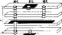
过孔是多层PCB设计中的一个重要因素,过孔主要由三部分组成,一是孔;二是孔周围的焊盘区;三是POWER层隔离区,过孔的工艺过程是在过孔的孔壁圆柱面上用化学沉积的方法镀上一层金属,用以连通中间各层需要连通的铜箔,而过孔的上下两面做成普通的焊盘形状,可直接与上下两面的线路相通,也可不连。过孔可以起到电气连接,固定或定位器件的作用。过孔结构示意图如图1所示:Vias are an important factor in multilayer PCB design. Vias are mainly composed of three parts, one is the hole; the other is the pad area around the hole; the third is the isolation area of the POWER layer. The cylindrical surface of the hole wall is plated with a layer of metal by chemical deposition to connect the copper foils that need to be connected in the middle layer, and the upper and lower sides of the via hole are made into ordinary pad shapes, which can be directly connected to the upper and lower sides of the circuit. Connected, or not connected. Vias can be used to electrically connect, fix or position devices. The schematic diagram of the via structure is shown in Figure 1:
过孔一般又分为三类:盲孔、埋孔和通孔。Vias are generally divided into three categories: blind vias, buried vias, and through vias.
盲孔,指位于印刷线路板的顶层和底层表面,具有一定深度,用于表层线路和下面的内层线路的连接,孔的深度与孔径通常不超过一定的比率。Blind holes refer to the top and bottom surfaces of the printed circuit board, with a certain depth, and are used to connect the surface circuit and the inner layer circuit below. The depth and diameter of the hole usually do not exceed a certain ratio.
埋孔,指位于印刷线路板内层的连接孔,它不会延伸到线路板的表面。Buried hole refers to the connection hole located in the inner layer of the printed circuit board, which does not extend to the surface of the circuit board.
通孔,这种孔穿过整个线路板,可用于实现内部互连或作为元件的安装定位孔。由于通孔在工艺上更易于实现,成本较低,所以一般印制电路板均使用通孔。过孔的分类如下图2所示。Through holes, which pass through the entire circuit board, can be used for internal interconnection or as mounting positioning holes for components. Since the through hole is easier to realize in the process and the cost is lower, the general printed circuit board uses the through hole. The classification of vias is shown in Figure 2 below.
过孔本身存在着对地的寄生电容,若过孔在铺地层上的隔离孔直径为D2,过孔焊盘的直径为D1,PCB的厚度为T,板基材介电常数为ε,则过孔的寄生电容大小近似于:C=1.41εTD1/(D2-D1)The via hole itself has a parasitic capacitance to the ground. If the diameter of the isolation hole of the via hole on the ground layer is D2 , the diameter of the via pad is D1 , the thickness of the PCB is T, and the dielectric constant of the board substrate is ε , then the parasitic capacitance of the via is approximately: C=1.41εTD1 /(D2 -D1 )
过孔的寄生电容会给电路造成的主要影响是延长了信号的上升时间,降低了电路的速度,容值越小则影响越小。信号线上的过孔影响信号传输速度,增大了信号传输延迟。The main impact of the parasitic capacitance of the via on the circuit is to prolong the rise time of the signal and reduce the speed of the circuit. The smaller the capacitance, the smaller the impact. The vias on the signal line affect the signal transmission speed and increase the signal transmission delay.
过孔本身就存在寄生电感,在高速数字电路的设计中,过孔的寄生电感带来的危害往往大于寄生电容的影响。过孔的寄生串联电感会削弱旁路电容的作用,减弱整个电源系统的滤波效用,引起转换噪声,噪声是由电流的瞬态变化和电源、地分布的有限阻抗最终导致的。随着器件中电源或地的电流的变化,当芯片逻辑开关或一个I/O驱动器开关时,使得互连的电感上有一个压降通过。这个压降降低了芯片的电源电压,使得它们的门延缓慢下来,从而降低了可工作的最高频率,电源和地的分布电感是取得高时钟频率的必要组成部分。The via itself has parasitic inductance. In the design of high-speed digital circuits, the harm caused by the parasitic inductance of the via is often greater than the influence of the parasitic capacitance. The parasitic series inductance of the via hole will weaken the effect of the bypass capacitor, weaken the filtering effect of the entire power system, and cause conversion noise. The noise is finally caused by the transient change of the current and the finite impedance of the power supply and ground distribution. As the power or ground current in the device changes, when the chip logic switches or an I/O driver switches, it causes a voltage drop across the inductance of the interconnect. This voltage drop reduces the power supply voltage of the chips, slowing down their gate delays, thereby reducing the maximum frequency at which they can operate. The distributed inductance of the power supply and ground is a necessary component to achieve high clock frequencies.
若L指过孔的电感,h是过孔的长度,d是中心钻孔的直径,过孔的寄生电感近似于:L=5.08h[ln(4h/d)+1]If L refers to the inductance of the via, h is the length of the via, and d is the diameter of the center drilled hole, the parasitic inductance of the via is approximately: L=5.08h[ln(4h/d)+1]
从式中可以看出,过孔的直径对电感的影响较小,而对电感影响最大的是过孔的长度。It can be seen from the formula that the diameter of the via hole has little influence on the inductance, and the length of the via hole has the greatest influence on the inductance.
现有使用印制板HDI工艺技术。HDI:High Density Interconnect,高密度互连,也称BUM(Build-up Multilayer或Build-up PCB),即积层法多层板。积层互联通常采用微孔技术。下图3是HDI印制板结构示意图。The existing printed board HDI process technology is used. HDI: High Density Interconnect, high-density interconnection, also known as BUM (Build-up Multilayer or Build-up PCB), that is, build-up multilayer board. Build-up interconnects typically use microvia technology. Figure 3 below is a schematic diagram of the HDI printed board structure.
芯层,HDI印制板中用来做内芯的普通层。Core layer, the ordinary layer used as the inner core in HDI printed boards.
积层,叠积于芯层表面的高密互联层,通常采用微孔技术。Build-up, a high-density interconnection layer stacked on the surface of the core layer, usually using microporous technology.
微孔底部对应Capture Pad:微孔顶部对应Pad。The bottom of the microwell corresponds to the Capture Pad: the top of the microwell corresponds to the Pad.
埋孔,没有延伸到PCB表面的导通孔。Buried vias, vias that do not extend to the surface of the PCB.
HDI关键技术是微孔的成孔,常用的成孔方式主要有三种:等离子成孔、感光成孔、激光成孔。The key technology of HDI is micropore forming. There are three commonly used hole forming methods: plasma hole forming, photosensitive hole forming, and laser hole forming.
其中激光成孔是目前HDI印制版工业中采用最多的成孔技术,它是利用材料对激光能量的吸收性能,将介质材料汽化、炭化,或者打破有机材料的分子长链;然后清洗、金属化的过程。Among them, laser pore forming is the most widely used pore forming technology in the HDI printing plate industry. It uses the absorption properties of materials for laser energy to vaporize and carbonize dielectric materials, or break the long molecular chains of organic materials; then clean, metal process.
目前国内激光成孔技术采用的激光源一般有两种:UV-YAG激光和CO2激光,其中UV-YAG激光光谱范围在紫外光部分,而CO2激光光谱则落在红外部分。两者的成孔外在表现区别在于前者可以打穿铜箔,而后者则不能打穿铜箔。At present, there are generally two types of laser sources used in domestic laser hole forming technology: UV-YAG laser and CO2 laser. The UV-YAG laser spectrum ranges in the ultraviolet part, while the CO2 laser spectrum falls in the infrared part. The difference in the external performance of the hole formation between the two is that the former can penetrate copper foil, while the latter cannot penetrate copper foil.
激光成孔相对于传统通孔印制板加工,加工流程复杂。以1+4+1的激光成孔6层HDI板为例。加工流程如下图4示:需要经过裁板、蚀刻L3+L4层线路,其次冲定位孔、AOI检查,再次加铜泊、PP、并于其上进行压板,在进行钻孔、蚀刻L2、L5层线路,并将孔金属化、塞孔等,再叠加RCC、钻CONFORMAL孔、与机械定位孔,然后CONFORMAL、钻镭射孔、钻通孔,最后进行镀孔、蚀刻外层线路,完成后制程,同多层板作业。Compared with the traditional through-hole printed board processing, the laser forming hole has a complicated processing process. Take 1+4+1 laser-holed 6-layer HDI board as an example. The processing flow is shown in Figure 4 below: it needs to cut the board, etch the L3+L4 layer circuit, then punch the positioning hole, AOI inspection, add copper and PP again, and press the plate on it, and then drill and etch L2 and L5 layer circuit, metallize the hole, plug the hole, etc., then superimpose RCC, drill CONFORMAL hole, and mechanical positioning hole, then CONFORMAL, drill laser hole, drill through hole, and finally plate the hole and etch the outer layer circuit, and complete the post-production process , with the multi-layer board operation.
微孔成孔工艺控制复杂,良品率较低:因为微孔钻孔较小,则PCB板厚与成孔径比不能过大,一方面介质太厚,则孔壁质量形成不好,残胶量较大;另一方面由于表面张力原因,药水流动困难,孔金属化困难。The control of micro-hole forming process is complicated, and the yield rate is low: because the micro-hole drilling is small, the ratio of PCB thickness to hole diameter cannot be too large. On the one hand, the medium is too thick, and the quality of the hole wall is not good, and the amount of residual glue Larger; on the other hand, due to the surface tension, the flow of the liquid medicine is difficult, and the hole metallization is difficult.
另外对大量埋孔塞孔工艺难以控制,塞孔质量不好出现塞孔凸起或内缩。这类埋孔在环境实验后极有可能出现断裂或者使线路断开。对常用的激光成孔工艺,其激光源一般有两种:CO2激光和UV激光。CO2激光波长10.6和9.4um(9.4um能量更高),属于红外线区域。其特点是:可以打穿介质,不能打穿铜箔,在成孔前,必须先在铜箔开窗;成孔的机理是烧蚀,因而在孔壁和孔底形成“焦化”和残留物,金属化前必须做好去焦渣处理。随孔深增加,烧蚀的能量需加强,易引起更多焦渣,并易引起底部铜箔与介质分层,因此不适合做小孔深孔(一般孔径≥80um);对玻璃纤维布比较难烧蚀。In addition, it is difficult to control the process of plugging a large number of buried holes, and the quality of the plug holes is not good, and the plug holes are raised or retracted. Such buried vias are very likely to break or disconnect the line after environmental testing. For the commonly used laser hole forming process, there are generally two types of laser sources:CO2 laser and UV laser. The wavelength of CO2 laser is 10.6 and 9.4um (9.4um has higher energy), which belongs to the infrared region. Its characteristics are: it can penetrate the medium, but not the copper foil. Before forming a hole, you must first open a window on the copper foil; the mechanism of forming a hole is ablation, so "coking" and residues are formed on the wall and bottom of the hole. , Before metallization, de-coking residue treatment must be done. As the hole depth increases, the ablation energy needs to be strengthened, which will easily cause more slag and delamination between the bottom copper foil and the medium, so it is not suitable for small deep holes (generally, the hole diameter is ≥ 80um); compared with glass fiber cloth Difficult to ablate.
UV激光采用固态光源(如Nd:YAG),波长0.355um或0.266um,属于紫外线区域。其特点是:可以加工铜、介质和玻璃布,因此不需在铜箔先开窗,对1080等加工能力较好;成孔机理是破坏物质的结构键成孔,因而孔壁和孔底光洁,活性高,可直接金属化;对比CO2激光,可加工孔径更小(一般≤100um),深度更深;但孔径≥100um时,加工效率低,成本高,因此目前最常用的依然是CO2激光。UV laser uses a solid-state light source (such as Nd:YAG), with a wavelength of 0.355um or 0.266um, which belongs to the ultraviolet region. Its characteristics are: it can process copper, dielectric and glass cloth, so it is not necessary to open the window on the copper foil first, and the processing ability for 1080 is better; the hole-forming mechanism is to destroy the structural bond of the material to form holes, so the hole walls and bottoms are smooth , high activity, and can be directly metallized; compared with CO2 laser, the machining aperture is smaller (generally ≤100um), and the depth is deeper; but when the aperture is ≥100um, the processing efficiency is low and the cost is high, so the most commonly used one is still CO2 laser.
加工成本比较高昂:HDI PCB成本所受影响因数和普通刚性PCB一致外(如PCB层数、尺寸、板材利用率等),还受积层层数、埋孔结构、微孔结构等因素影响。如对于一个8层HDI板来讲,其不同的结构成本差异如下(此数据仅供参考):The processing cost is relatively high: HDI PCB cost is affected by the same factors as ordinary rigid PCB (such as the number of PCB layers, size, board utilization, etc.), and is also affected by factors such as the number of layers, buried hole structure, and microhole structure. For example, for an 8-layer HDI board, the cost difference of different structures is as follows (this data is for reference only):
(1)1+6+1(有2~7的机械埋孔):成本基数1(1) 1+6+1 (with 2 to 7 mechanical buried holes):
(2)2+4+2(错开孔,有3~6的机械埋孔):1.5(2) 2+4+2 (staggered holes, with 3~6 mechanical buried holes): 1.5
(3)2+4+2(错开孔,有3~6、2~7的机械埋孔):1.7(3) 2+4+2 (staggered holes, with 3~6, 2~7 mechanical buried holes): 1.7
(4)2+4+2(微叠孔,有3~6的机械埋孔):1.9(4) 2+4+2 (micro-stacked holes, with 3 to 6 mechanical buried holes): 1.9
(5)2+4+2(微叠孔,有3~6、2~7的机械埋孔):2.1(5) 2+4+2 (micro-stacked holes, with 3~6, 2~7 mechanical buried holes): 2.1
另外使用HDI工艺的装配成品板信号测试覆盖率也相对较低,如对细间距面阵列器件区域内的测试点无法采用通孔测试点。In addition, the signal test coverage of the assembled finished board using the HDI process is relatively low. For example, through-hole test points cannot be used for the test points in the area of the fine-pitch area array device.
基于以上缺陷,从业界统计来看,目前HDI印制板主要应用于手机板和封装基板,在大尺寸的系统级高可靠复杂印制板中应用较少。Based on the above defects, according to industry statistics, HDI printed boards are currently mainly used in mobile phone boards and packaging substrates, and are rarely used in large-scale system-level high-reliability and complex printed boards.
发明内容Contents of the invention
本发明的一个目的在于,针对现有复合印制电路板的不足,提供一种可实现高速信号传输的印制电路板,降低成本;本发明的另一个目的在于,还提供一种制作上述电路板的的方法。One object of the present invention is to provide a printed circuit board that can realize high-speed signal transmission and reduce costs in view of the shortcomings of the existing composite printed circuit board; another object of the present invention is to provide a method for making the above circuit board method.
本发明提供的技术方案如下:提供一种可实现高速信号传输的印制电路板,由多层板复合构成,构成所述印制电路板的两个外层是能传输高速信号的板材层,内层是普通板材层。The technical solution provided by the present invention is as follows: provide a printed circuit board that can realize high-speed signal transmission, which is composed of multi-layer boards, and the two outer layers that constitute the printed circuit board are plate layers that can transmit high-speed signals, The inner layer is a common board layer.
一种制作上述可实现高速信号传输的印制电路板的方法,采用层压的方式在普通板材层外侧形成能传输高速信号的板材层,然后钻通孔,金属化,最后形成多层的印制电路板。A method for manufacturing the above-mentioned printed circuit board that can realize high-speed signal transmission, adopting a lamination method to form a board layer capable of transmitting high-speed signals on the outside of the ordinary board layer, then drilling through holes, metallization, and finally forming a multi-layer printed circuit board. circuit board.
具体步骤包括如下:The specific steps include the following:
1)、对所述普通板材层进行黑化或棕化处理;1), blackening or browning treatment is carried out to the common board layer;
2)、加入半固化片与外层铜箔与内层普通板材层进行叠合与压合,形成能传输高速信号的外层板材层;2) Add the prepreg and the outer layer of copper foil to laminate and press the inner ordinary board layer to form an outer board layer capable of transmitting high-speed signals;
3)、对上述2)步骤形成的多层板,进行钻孔,镀通孔、在各内3), for the multi-layer board formed in the above 2) steps, drill holes, plate through holes,
层板上通过底片成像与蚀刻,作出所需的导通线路及外层线路,进而制得印刷电路板。Through negative film imaging and etching on the layer board, the required conduction lines and outer layer lines are made, and then the printed circuit board is produced.
本发明具有如下优点:将多层结构的印刷电路板采用特殊板材与普通板材混压后制得复合印刷电路板,既可以实现高速信号传输,又可以降低电路板的成本,板材混压技术不但可以降低成本,而且可以解决高速特殊板材的局限性,如部分材料厚度规格少、后续PCBA组装难度高等问题;The invention has the following advantages: the printed circuit board with multi-layer structure is mixed and pressed with special plates and common plates to make a composite printed circuit board, which can not only realize high-speed signal transmission, but also reduce the cost of the circuit board. It can reduce costs and solve the limitations of high-speed special boards, such as the small thickness of some materials and the difficulty of subsequent PCBA assembly;
在制作这种结构的电路板时,可对高速信号过孔使用背钻工艺,以去掉过孔端部的无连接无属性的STUB;实现低成本、高可靠性的高速信号印制电路板设计方案,传统多层板的制作工艺,由于只需一次层压、一次钻孔,因此工序比较简单,PCB制作良品率及高速信号的传输质量均可得到保证。When making a circuit board with this structure, the back-drilling process can be used for the high-speed signal via hole to remove the non-connected and non-attribute STUB at the end of the via hole; realize low-cost, high-reliability high-speed signal printed circuit board design Solution, the traditional multi-layer board manufacturing process, because only one lamination and one drilling is required, so the process is relatively simple, and the yield rate of PCB production and the transmission quality of high-speed signals can be guaranteed.
附图说明Description of drawings
图1是多层电路板中过孔示意图;Figure 1 is a schematic diagram of vias in a multilayer circuit board;
图2是图1所示各种过孔结构示意图;FIG. 2 is a schematic diagram of various via structures shown in FIG. 1;
图3是本发明方法中多层电路板的结构示意图;Fig. 3 is the structural representation of multilayer circuit board in the inventive method;
图4是本发明方法中多层电路板制作流程图;Fig. 4 is the flow chart of making multilayer circuit board in the inventive method;
图5是图4所示制作流程图中背钻工艺示意图;Fig. 5 is a schematic diagram of the back-drilling process in the production flow chart shown in Fig. 4;
图6是采用背钻完成的微孔短导通孔长度使得接地电感降低,有效地改善了开关噪声的对比示意图。FIG. 6 is a comparison schematic diagram of the short via length of the microvia completed by back drilling, which reduces the grounding inductance and effectively improves the switching noise.
具体实施方式Detailed ways
参照图1、图2、图3、图4、图5、图6,一般PCB上高速信号的传输线只是局部的,PCB的部分层可以不使用高档材料,而使用价格相对较低,并且传输信号的性能较普通的普通材料板材如FR4构成电路板的多个内层,综合信号质量要求、仿真结果及成本、厂商工艺成熟度各方面因素,可采用板材混压技术,混压结构相比于通常结构,在成本、性能、可获得性等方面具有更多的灵活性和适应性,如图3所示,为实现高速信号的特殊板材ROGERS4350与普通板材FR4的八层板混压结构:两个外层采用是能传输高速信号的ROGERS4350特殊板材,6个内层板采用FR4普通板材;可大大降低电路板的材料成本。Referring to Figure 1, Figure 2, Figure 3, Figure 4, Figure 5, and Figure 6, the transmission line of high-speed signals on the general PCB is only partial, and some layers of the PCB may not use high-grade materials, but the use price is relatively low, and the transmission signal The performance is more common than that of ordinary common material plates such as FR4, which constitute the multiple inner layers of the circuit board. Considering the signal quality requirements, simulation results and costs, and the maturity of the manufacturer's process, the plate mixed pressure technology can be used. The mixed pressure structure is compared with The general structure has more flexibility and adaptability in terms of cost, performance, availability, etc. The 1 outer layer is made of ROGERS4350 special plate that can transmit high-speed signals, and the 6 inner layers are made of FR4 ordinary plate; which can greatly reduce the material cost of the circuit board.
使用传统多层板制作方法完成PCB板的加工,传统多层板的制作方法是层压内层来形成多层板,然后钻通孔,金属化并制作外层线路。其流程可以概要为以下几步:The processing of the PCB board is completed using the traditional multi-layer board manufacturing method. The traditional multi-layer board manufacturing method is to laminate the inner layer to form a multi-layer board, then drill through holes, metallize and make the outer layer circuit. The process can be summarized as the following steps:
在各内层芯板上通过底片成像与蚀刻,作出所需的导通线路如焊盘(Pad);Make the required conduction lines such as pads (Pad) through negative film imaging and etching on each inner core board;
对内层芯板进行黑化/棕化处理(Black/Brown Oxide Treament),完成各内层板;Black/Brown Oxide Treament is performed on the inner core board to complete each inner board;
加入半固化片与外层铜箔进行叠合与压合,形成多层半成品板;Add the prepreg and the outer layer of copper foil for lamination and pressing to form a multi-layer semi-finished board;
再进行钻孔,镀通孔(PTH)、底片成像(Image Transfer,正片法或负片法)以及蚀刻得到外层线路并完成多层板之成品。详细步骤如图4所示;Drilling, plated through holes (PTH), negative film imaging (Image Transfer, positive film method or negative film method) and etching to obtain the outer layer circuit and complete the finished product of the multilayer board. The detailed steps are shown in Figure 4;
对部分高速信号过孔使用背钻(Back Drill)工艺Use back drilling (Back Drill) process for some high-speed signal vias
采用背钻方式钻孔(Back Drill)是将过孔端部的无连接属性的STUB钻掉;由于信号线上的过孔总体表现为容性,使得阻抗降低。背钻(Back Drill)完成的微孔对阻抗的影响较通孔要小。Back Drilling is to drill off the non-connected STUB at the end of the via; since the vias on the signal line are generally capacitive, the impedance is reduced. Microholes completed by Back Drill have less impact on impedance than through holes.
参照图6,背钻(Back Drill)完成的微孔短导通孔长度使得接地电感降低,可有效地改善开关噪声。Referring to Figure 6, the short via length of the microvias completed by Back Drill reduces the grounding inductance, which can effectively improve the switching noise.
除上述方法外,还可以通过下列方法来实现高速信号传输:In addition to the above methods, high-speed signal transmission can also be achieved by the following methods:
改变过孔背钻深度来实现高速信号传输;Change the back-drilling depth of vias to achieve high-speed signal transmission;
通过改变过孔背钻剩余孔壁的长度也可以实现高速信号传输;High-speed signal transmission can also be achieved by changing the length of the remaining wall of the back-drilled via hole;
通过改变过孔背钻孔径也可以实现高速信号传输;High-speed signal transmission can also be achieved by changing the back-drilled aperture of the via;
通过改变距离背钻孔径最近的走线层距离也可以实现高速信号传输。High-speed signal transmission can also be achieved by changing the distance of the trace layer closest to the back-drilled aperture.
Claims (9)
Priority Applications (1)
| Application Number | Priority Date | Filing Date | Title |
|---|---|---|---|
| CN 200510101738CN1852633A (en) | 2005-11-21 | 2005-11-21 | Printed circuit board capable of realizing high-speed signal transmission and making method |
Applications Claiming Priority (1)
| Application Number | Priority Date | Filing Date | Title |
|---|---|---|---|
| CN 200510101738CN1852633A (en) | 2005-11-21 | 2005-11-21 | Printed circuit board capable of realizing high-speed signal transmission and making method |
Publications (1)
| Publication Number | Publication Date |
|---|---|
| CN1852633Atrue CN1852633A (en) | 2006-10-25 |
Family
ID=37134095
Family Applications (1)
| Application Number | Title | Priority Date | Filing Date |
|---|---|---|---|
| CN 200510101738PendingCN1852633A (en) | 2005-11-21 | 2005-11-21 | Printed circuit board capable of realizing high-speed signal transmission and making method |
Country Status (1)
| Country | Link |
|---|---|
| CN (1) | CN1852633A (en) |
Cited By (25)
| Publication number | Priority date | Publication date | Assignee | Title |
|---|---|---|---|---|
| WO2009089709A1 (en)* | 2007-12-14 | 2009-07-23 | Huawei Technologies Co., Ltd. | Printed circuit board, manufacturing method and radio-frequency apparatus thereof |
| CN101815404A (en)* | 2010-04-08 | 2010-08-25 | 梅州五洲电路板有限公司 | High-frequency mixed compression process for printed circuit board |
| CN102043121A (en)* | 2010-07-21 | 2011-05-04 | 北大方正集团有限公司 | Detection method for circuit board back drill hole and test equipment for detecting circuit board back drill hole |
| CN102056404A (en)* | 2010-11-15 | 2011-05-11 | 浪潮电子信息产业股份有限公司 | Method for neutralizing capacitance of through hole |
| CN102215628A (en)* | 2011-03-09 | 2011-10-12 | 华为技术有限公司 | Super-thick circuit board |
| CN101772269B (en)* | 2009-12-23 | 2011-10-12 | 深南电路有限公司 | PCB (Printed Circuit Board) processing method |
| CN101666854B (en)* | 2009-09-30 | 2011-12-28 | 深南电路有限公司 | Detecting method for back drilling and missed drilling |
| CN102300412A (en)* | 2011-08-19 | 2011-12-28 | 东莞生益电子有限公司 | PCB back drilling processing method |
| CN102438412A (en)* | 2011-11-14 | 2012-05-02 | 东莞生益电子有限公司 | Back drilling processing method of PCB |
| CN102779197A (en)* | 2011-05-13 | 2012-11-14 | 鸿富锦精密工业(深圳)有限公司 | Parasitic inductance inspection system and method |
| CN102835196A (en)* | 2010-03-31 | 2012-12-19 | 弗莱克斯电子有限责任公司 | Improved backdrilling of multilayer printed circuit boards |
| CN103002674A (en)* | 2012-09-03 | 2013-03-27 | 杭州华三通信技术有限公司 | PCB (printed circuit board) back drilling method and PCB through hole structure |
| CN103269564A (en)* | 2013-03-28 | 2013-08-28 | 淳华科技(昆山)有限公司 | Multilayer board local single-layer area inner layer cutting process |
| CN103298251A (en)* | 2013-05-23 | 2013-09-11 | 华为技术有限公司 | Printed circuit board and production method thereof |
| CN103384455A (en)* | 2012-05-03 | 2013-11-06 | 旭德科技股份有限公司 | Method for manufacturing substrate structure |
| CN104182593A (en)* | 2014-09-04 | 2014-12-03 | 浪潮电子信息产业股份有限公司 | Printed circuit board (PCB) design method with good cost performance ratio |
| WO2017156678A1 (en)* | 2016-03-14 | 2017-09-21 | 深圳崇达多层线路板有限公司 | Method for manufacturing stacked holes of circuit board |
| CN107484362A (en)* | 2017-10-17 | 2017-12-15 | 珠海杰赛科技有限公司 | The processing method of digital-to-analogue printed wiring board |
| CN109362175A (en)* | 2018-11-30 | 2019-02-19 | 神思电子技术股份有限公司 | A kind of design method for the via hole reducing power supply ripple |
| CN109933931A (en)* | 2019-03-21 | 2019-06-25 | 浪潮商用机器有限公司 | A method of detecting whether the target layer of backdrilling is set correctly |
| CN112349668A (en)* | 2020-09-28 | 2021-02-09 | 中国电子科技集团公司第二十九研究所 | Broadband radio frequency module structure adopting radio frequency motherboard and design method thereof |
| CN112770508A (en)* | 2020-12-11 | 2021-05-07 | 广州广合科技股份有限公司 | Method for improving PCB back drilling depth precision |
| CN113133214A (en)* | 2021-04-07 | 2021-07-16 | 洛阳伟信电子科技有限公司 | Method for manufacturing asymmetric copper thick multilayer board |
| CN113964613A (en)* | 2021-12-16 | 2022-01-21 | 苏州浪潮智能科技有限公司 | A method, apparatus, apparatus and readable medium for reducing high-speed connector stub |
| CN114039270A (en)* | 2021-09-23 | 2022-02-11 | 苏州苏驼通信科技股份有限公司 | TO tube seat and preparation method thereof |
- 2005
- 2005-11-21CNCN 200510101738patent/CN1852633A/enactivePending
Cited By (35)
| Publication number | Priority date | Publication date | Assignee | Title |
|---|---|---|---|---|
| WO2009089709A1 (en)* | 2007-12-14 | 2009-07-23 | Huawei Technologies Co., Ltd. | Printed circuit board, manufacturing method and radio-frequency apparatus thereof |
| US8633393B2 (en) | 2007-12-14 | 2014-01-21 | Huawei Technologies Co., Ltd. | Printed circuit board, manufacturing method thereof and radio-frequency device |
| CN101460018B (en)* | 2007-12-14 | 2011-02-16 | 华为技术有限公司 | Printed circuit board, manufacturing method and radio-frequency apparatus thereof |
| EP2986088A1 (en)* | 2007-12-14 | 2016-02-17 | Huawei Technologies Co., Ltd. | Printed circuit board, manufacturing method thereof and radio-frequency device |
| CN101666854B (en)* | 2009-09-30 | 2011-12-28 | 深南电路有限公司 | Detecting method for back drilling and missed drilling |
| CN101772269B (en)* | 2009-12-23 | 2011-10-12 | 深南电路有限公司 | PCB (Printed Circuit Board) processing method |
| CN102835196A (en)* | 2010-03-31 | 2012-12-19 | 弗莱克斯电子有限责任公司 | Improved backdrilling of multilayer printed circuit boards |
| CN102835196B (en)* | 2010-03-31 | 2015-11-25 | 弗莱克斯电子有限责任公司 | The back-drilling of the improvement of multilayer board |
| CN101815404A (en)* | 2010-04-08 | 2010-08-25 | 梅州五洲电路板有限公司 | High-frequency mixed compression process for printed circuit board |
| CN102043121A (en)* | 2010-07-21 | 2011-05-04 | 北大方正集团有限公司 | Detection method for circuit board back drill hole and test equipment for detecting circuit board back drill hole |
| CN102056404A (en)* | 2010-11-15 | 2011-05-11 | 浪潮电子信息产业股份有限公司 | Method for neutralizing capacitance of through hole |
| CN102056404B (en)* | 2010-11-15 | 2013-01-23 | 浪潮电子信息产业股份有限公司 | Method for neutralizing capacitance of through hole |
| CN102215628A (en)* | 2011-03-09 | 2011-10-12 | 华为技术有限公司 | Super-thick circuit board |
| CN102779197A (en)* | 2011-05-13 | 2012-11-14 | 鸿富锦精密工业(深圳)有限公司 | Parasitic inductance inspection system and method |
| CN102300412A (en)* | 2011-08-19 | 2011-12-28 | 东莞生益电子有限公司 | PCB back drilling processing method |
| CN102438412B (en)* | 2011-11-14 | 2013-09-25 | 东莞生益电子有限公司 | Back drilling processing method of PCB |
| CN102438412A (en)* | 2011-11-14 | 2012-05-02 | 东莞生益电子有限公司 | Back drilling processing method of PCB |
| CN103384455A (en)* | 2012-05-03 | 2013-11-06 | 旭德科技股份有限公司 | Method for manufacturing substrate structure |
| CN103384455B (en)* | 2012-05-03 | 2016-03-02 | 旭德科技股份有限公司 | Method for manufacturing substrate structure |
| CN103002674A (en)* | 2012-09-03 | 2013-03-27 | 杭州华三通信技术有限公司 | PCB (printed circuit board) back drilling method and PCB through hole structure |
| CN103269564A (en)* | 2013-03-28 | 2013-08-28 | 淳华科技(昆山)有限公司 | Multilayer board local single-layer area inner layer cutting process |
| CN103269564B (en)* | 2013-03-28 | 2015-11-18 | 淳华科技(昆山)有限公司 | Multilayer board local single-layer area inner layer cutting technique |
| CN103298251B (en)* | 2013-05-23 | 2016-05-25 | 华为技术有限公司 | A kind of printed circuit board (PCB) and preparation method thereof |
| CN103298251A (en)* | 2013-05-23 | 2013-09-11 | 华为技术有限公司 | Printed circuit board and production method thereof |
| CN104182593A (en)* | 2014-09-04 | 2014-12-03 | 浪潮电子信息产业股份有限公司 | Printed circuit board (PCB) design method with good cost performance ratio |
| WO2017156678A1 (en)* | 2016-03-14 | 2017-09-21 | 深圳崇达多层线路板有限公司 | Method for manufacturing stacked holes of circuit board |
| CN107484362A (en)* | 2017-10-17 | 2017-12-15 | 珠海杰赛科技有限公司 | The processing method of digital-to-analogue printed wiring board |
| CN109362175A (en)* | 2018-11-30 | 2019-02-19 | 神思电子技术股份有限公司 | A kind of design method for the via hole reducing power supply ripple |
| CN109933931A (en)* | 2019-03-21 | 2019-06-25 | 浪潮商用机器有限公司 | A method of detecting whether the target layer of backdrilling is set correctly |
| CN112349668A (en)* | 2020-09-28 | 2021-02-09 | 中国电子科技集团公司第二十九研究所 | Broadband radio frequency module structure adopting radio frequency motherboard and design method thereof |
| CN112770508A (en)* | 2020-12-11 | 2021-05-07 | 广州广合科技股份有限公司 | Method for improving PCB back drilling depth precision |
| CN112770508B (en)* | 2020-12-11 | 2022-05-17 | 广州广合科技股份有限公司 | Method for improving PCB back drilling depth precision |
| CN113133214A (en)* | 2021-04-07 | 2021-07-16 | 洛阳伟信电子科技有限公司 | Method for manufacturing asymmetric copper thick multilayer board |
| CN114039270A (en)* | 2021-09-23 | 2022-02-11 | 苏州苏驼通信科技股份有限公司 | TO tube seat and preparation method thereof |
| CN113964613A (en)* | 2021-12-16 | 2022-01-21 | 苏州浪潮智能科技有限公司 | A method, apparatus, apparatus and readable medium for reducing high-speed connector stub |
Similar Documents
| Publication | Publication Date | Title |
|---|---|---|
| CN1852633A (en) | Printed circuit board capable of realizing high-speed signal transmission and making method | |
| KR100632554B1 (en) | Capacitor embedded printed circuit board and its manufacturing method | |
| US9711441B2 (en) | Reduced PTH pad for enabling core routing and substrate layer count reduction | |
| US8528203B2 (en) | Providing selective via plating using laser resin activation | |
| US6444922B1 (en) | Zero cross-talk signal line design | |
| TWI383715B (en) | High density package substrate and method for fabricating the same | |
| EP1878328A2 (en) | Apertures for signal shaping using ground and signal pth back-drilling | |
| CN103402332B (en) | PCB with high-density interconnection design and heat dissipation structure and manufacturing method thereof | |
| CN103369866B (en) | The manufacture method of a kind of printed wiring board containing blind hole and printed wiring board thereof | |
| CN110798988A (en) | Additive process for manufacturing high-frequency antenna packaging substrate and AiP packaging antenna structure | |
| CN103687306A (en) | A printed circuit board and its manufacturing method | |
| KR100716810B1 (en) | Capacitor-embedded printed circuit board with blind via hole and manufacturing method thereof | |
| US7629692B2 (en) | Via hole having fine hole land and method for forming the same | |
| WO2025138643A1 (en) | Method for making signal holes in through-hole board, and through-hole board manufacturing method and system | |
| JP2000216513A (en) | Wiring board and manufacturing method using the same | |
| CN201230403Y (en) | Printed circuit board | |
| KR100632579B1 (en) | How to Form Via Holes in Printed Circuit Boards | |
| CN108235585A (en) | Windowing method of prepreg, manufacturing method of high-speed backboard and high-speed backboard | |
| JP4802402B2 (en) | High-density multilayer build-up wiring board and manufacturing method thereof | |
| CN212628582U (en) | High-frequency radar plate structure | |
| CN220711712U (en) | Circuit board | |
| CN114286541B (en) | Processing method of HDI board, HDI board and electronic equipment | |
| CN117255503A (en) | Production process of radar circuit board | |
| US10764992B1 (en) | Circuit board and method for manufacturing the same | |
| JP2019029559A (en) | Multilayer wiring board and manufacturing method thereof |
Legal Events
| Date | Code | Title | Description |
|---|---|---|---|
| C06 | Publication | ||
| PB01 | Publication | ||
| C10 | Entry into substantive examination | ||
| SE01 | Entry into force of request for substantive examination | ||
| C12 | Rejection of a patent application after its publication | ||
| RJ01 | Rejection of invention patent application after publication |