CN1849853A - Substrate and its preparation method - Google Patents
Substrate and its preparation methodDownload PDFInfo
- Publication number
- CN1849853A CN1849853ACNA2004800260766ACN200480026076ACN1849853ACN 1849853 ACN1849853 ACN 1849853ACN A2004800260766 ACNA2004800260766 ACN A2004800260766ACN 200480026076 ACN200480026076 ACN 200480026076ACN 1849853 ACN1849853 ACN 1849853A
- Authority
- CN
- China
- Prior art keywords
- substrate
- metal
- silver
- scope
- preparing
- Prior art date
- Legal status (The legal status is an assumption and is not a legal conclusion. Google has not performed a legal analysis and makes no representation as to the accuracy of the status listed.)
- Pending
Links
Images

Classifications
- B—PERFORMING OPERATIONS; TRANSPORTING
- B05—SPRAYING OR ATOMISING IN GENERAL; APPLYING FLUENT MATERIALS TO SURFACES, IN GENERAL
- B05D—PROCESSES FOR APPLYING FLUENT MATERIALS TO SURFACES, IN GENERAL
- B05D1/00—Processes for applying liquids or other fluent materials
- B05D1/007—Processes for applying liquids or other fluent materials using an electrostatic field
- H—ELECTRICITY
- H05—ELECTRIC TECHNIQUES NOT OTHERWISE PROVIDED FOR
- H05K—PRINTED CIRCUITS; CASINGS OR CONSTRUCTIONAL DETAILS OF ELECTRIC APPARATUS; MANUFACTURE OF ASSEMBLAGES OF ELECTRICAL COMPONENTS
- H05K3/00—Apparatus or processes for manufacturing printed circuits
- H05K3/10—Apparatus or processes for manufacturing printed circuits in which conductive material is applied to the insulating support in such a manner as to form the desired conductive pattern
- H05K3/12—Apparatus or processes for manufacturing printed circuits in which conductive material is applied to the insulating support in such a manner as to form the desired conductive pattern using thick film techniques, e.g. printing techniques to apply the conductive material or similar techniques for applying conductive paste or ink patterns
- B—PERFORMING OPERATIONS; TRANSPORTING
- B32—LAYERED PRODUCTS
- B32B—LAYERED PRODUCTS, i.e. PRODUCTS BUILT-UP OF STRATA OF FLAT OR NON-FLAT, e.g. CELLULAR OR HONEYCOMB, FORM
- B32B15/00—Layered products comprising a layer of metal
- B32B15/04—Layered products comprising a layer of metal comprising metal as the main or only constituent of a layer, which is next to another layer of the same or of a different material
- B32B15/08—Layered products comprising a layer of metal comprising metal as the main or only constituent of a layer, which is next to another layer of the same or of a different material of synthetic resin
- B—PERFORMING OPERATIONS; TRANSPORTING
- B32—LAYERED PRODUCTS
- B32B—LAYERED PRODUCTS, i.e. PRODUCTS BUILT-UP OF STRATA OF FLAT OR NON-FLAT, e.g. CELLULAR OR HONEYCOMB, FORM
- B32B3/00—Layered products comprising a layer with external or internal discontinuities or unevennesses, or a layer of non-planar shape; Layered products comprising a layer having particular features of form
- B32B3/26—Layered products comprising a layer with external or internal discontinuities or unevennesses, or a layer of non-planar shape; Layered products comprising a layer having particular features of form characterised by a particular shape of the outline of the cross-section of a continuous layer; characterised by a layer with cavities or internal voids ; characterised by an apertured layer
- B32B3/266—Layered products comprising a layer with external or internal discontinuities or unevennesses, or a layer of non-planar shape; Layered products comprising a layer having particular features of form characterised by a particular shape of the outline of the cross-section of a continuous layer; characterised by a layer with cavities or internal voids ; characterised by an apertured layer characterised by an apertured layer, the apertures going through the whole thickness of the layer, e.g. expanded metal, perforated layer, slit layer regular cells B32B3/12
- H—ELECTRICITY
- H01—ELECTRIC ELEMENTS
- H01L—SEMICONDUCTOR DEVICES NOT COVERED BY CLASS H10
- H01L21/00—Processes or apparatus adapted for the manufacture or treatment of semiconductor or solid state devices or of parts thereof
- H01L21/02—Manufacture or treatment of semiconductor devices or of parts thereof
- H01L21/04—Manufacture or treatment of semiconductor devices or of parts thereof the devices having potential barriers, e.g. a PN junction, depletion layer or carrier concentration layer
- H01L21/48—Manufacture or treatment of parts, e.g. containers, prior to assembly of the devices, using processes not provided for in a single one of the groups H01L21/18 - H01L21/326 or H10D48/04 - H10D48/07
- H01L21/4814—Conductive parts
- H01L21/4846—Leads on or in insulating or insulated substrates, e.g. metallisation
- H01L21/4867—Applying pastes or inks, e.g. screen printing
- H—ELECTRICITY
- H05—ELECTRIC TECHNIQUES NOT OTHERWISE PROVIDED FOR
- H05K—PRINTED CIRCUITS; CASINGS OR CONSTRUCTIONAL DETAILS OF ELECTRIC APPARATUS; MANUFACTURE OF ASSEMBLAGES OF ELECTRICAL COMPONENTS
- H05K3/00—Apparatus or processes for manufacturing printed circuits
- H05K3/10—Apparatus or processes for manufacturing printed circuits in which conductive material is applied to the insulating support in such a manner as to form the desired conductive pattern
- H05K3/12—Apparatus or processes for manufacturing printed circuits in which conductive material is applied to the insulating support in such a manner as to form the desired conductive pattern using thick film techniques, e.g. printing techniques to apply the conductive material or similar techniques for applying conductive paste or ink patterns
- H05K3/1241—Apparatus or processes for manufacturing printed circuits in which conductive material is applied to the insulating support in such a manner as to form the desired conductive pattern using thick film techniques, e.g. printing techniques to apply the conductive material or similar techniques for applying conductive paste or ink patterns by ink-jet printing or drawing by dispensing
- H05K3/125—Apparatus or processes for manufacturing printed circuits in which conductive material is applied to the insulating support in such a manner as to form the desired conductive pattern using thick film techniques, e.g. printing techniques to apply the conductive material or similar techniques for applying conductive paste or ink patterns by ink-jet printing or drawing by dispensing by ink-jet printing
- H—ELECTRICITY
- H05—ELECTRIC TECHNIQUES NOT OTHERWISE PROVIDED FOR
- H05K—PRINTED CIRCUITS; CASINGS OR CONSTRUCTIONAL DETAILS OF ELECTRIC APPARATUS; MANUFACTURE OF ASSEMBLAGES OF ELECTRICAL COMPONENTS
- H05K3/00—Apparatus or processes for manufacturing printed circuits
- H05K3/40—Forming printed elements for providing electric connections to or between printed circuits
- H—ELECTRICITY
- H05—ELECTRIC TECHNIQUES NOT OTHERWISE PROVIDED FOR
- H05K—PRINTED CIRCUITS; CASINGS OR CONSTRUCTIONAL DETAILS OF ELECTRIC APPARATUS; MANUFACTURE OF ASSEMBLAGES OF ELECTRICAL COMPONENTS
- H05K3/00—Apparatus or processes for manufacturing printed circuits
- H05K3/46—Manufacturing multilayer circuits
- H05K3/4644—Manufacturing multilayer circuits by building the multilayer layer by layer, i.e. build-up multilayer circuits
- H05K3/4647—Manufacturing multilayer circuits by building the multilayer layer by layer, i.e. build-up multilayer circuits by applying an insulating layer around previously made via studs
- H—ELECTRICITY
- H01—ELECTRIC ELEMENTS
- H01L—SEMICONDUCTOR DEVICES NOT COVERED BY CLASS H10
- H01L2924/00—Indexing scheme for arrangements or methods for connecting or disconnecting semiconductor or solid-state bodies as covered by H01L24/00
- H01L2924/0001—Technical content checked by a classifier
- H01L2924/0002—Not covered by any one of groups H01L24/00, H01L24/00 and H01L2224/00
- H—ELECTRICITY
- H05—ELECTRIC TECHNIQUES NOT OTHERWISE PROVIDED FOR
- H05K—PRINTED CIRCUITS; CASINGS OR CONSTRUCTIONAL DETAILS OF ELECTRIC APPARATUS; MANUFACTURE OF ASSEMBLAGES OF ELECTRICAL COMPONENTS
- H05K2201/00—Indexing scheme relating to printed circuits covered by H05K1/00
- H05K2201/03—Conductive materials
- H05K2201/0332—Structure of the conductor
- H05K2201/0364—Conductor shape
- H05K2201/0367—Metallic bump or raised conductor not used as solder bump
- H—ELECTRICITY
- H05—ELECTRIC TECHNIQUES NOT OTHERWISE PROVIDED FOR
- H05K—PRINTED CIRCUITS; CASINGS OR CONSTRUCTIONAL DETAILS OF ELECTRIC APPARATUS; MANUFACTURE OF ASSEMBLAGES OF ELECTRICAL COMPONENTS
- H05K2203/00—Indexing scheme relating to apparatus or processes for manufacturing printed circuits covered by H05K3/00
- H05K2203/01—Tools for processing; Objects used during processing
- H05K2203/0104—Tools for processing; Objects used during processing for patterning or coating
- H05K2203/013—Inkjet printing, e.g. for printing insulating material or resist
- H—ELECTRICITY
- H05—ELECTRIC TECHNIQUES NOT OTHERWISE PROVIDED FOR
- H05K—PRINTED CIRCUITS; CASINGS OR CONSTRUCTIONAL DETAILS OF ELECTRIC APPARATUS; MANUFACTURE OF ASSEMBLAGES OF ELECTRICAL COMPONENTS
- H05K2203/00—Indexing scheme relating to apparatus or processes for manufacturing printed circuits covered by H05K3/00
- H05K2203/10—Using electric, magnetic and electromagnetic fields; Using laser light
- H05K2203/105—Using an electrical field; Special methods of applying an electric potential
- H—ELECTRICITY
- H05—ELECTRIC TECHNIQUES NOT OTHERWISE PROVIDED FOR
- H05K—PRINTED CIRCUITS; CASINGS OR CONSTRUCTIONAL DETAILS OF ELECTRIC APPARATUS; MANUFACTURE OF ASSEMBLAGES OF ELECTRICAL COMPONENTS
- H05K2203/00—Indexing scheme relating to apparatus or processes for manufacturing printed circuits covered by H05K3/00
- H05K2203/11—Treatments characterised by their effect, e.g. heating, cooling, roughening
- H05K2203/1131—Sintering, i.e. fusing of metal particles to achieve or improve electrical conductivity
- H—ELECTRICITY
- H05—ELECTRIC TECHNIQUES NOT OTHERWISE PROVIDED FOR
- H05K—PRINTED CIRCUITS; CASINGS OR CONSTRUCTIONAL DETAILS OF ELECTRIC APPARATUS; MANUFACTURE OF ASSEMBLAGES OF ELECTRICAL COMPONENTS
- H05K2203/00—Indexing scheme relating to apparatus or processes for manufacturing printed circuits covered by H05K3/00
- H05K2203/14—Related to the order of processing steps
- H05K2203/1476—Same or similar kind of process performed in phases, e.g. coarse patterning followed by fine patterning
- H—ELECTRICITY
- H05—ELECTRIC TECHNIQUES NOT OTHERWISE PROVIDED FOR
- H05K—PRINTED CIRCUITS; CASINGS OR CONSTRUCTIONAL DETAILS OF ELECTRIC APPARATUS; MANUFACTURE OF ASSEMBLAGES OF ELECTRICAL COMPONENTS
- H05K3/00—Apparatus or processes for manufacturing printed circuits
- H05K3/22—Secondary treatment of printed circuits
- H05K3/24—Reinforcing the conductive pattern
- H05K3/245—Reinforcing conductive patterns made by printing techniques or by other techniques for applying conductive pastes, inks or powders; Reinforcing other conductive patterns by such techniques
- H—ELECTRICITY
- H05—ELECTRIC TECHNIQUES NOT OTHERWISE PROVIDED FOR
- H05K—PRINTED CIRCUITS; CASINGS OR CONSTRUCTIONAL DETAILS OF ELECTRIC APPARATUS; MANUFACTURE OF ASSEMBLAGES OF ELECTRICAL COMPONENTS
- H05K3/00—Apparatus or processes for manufacturing printed circuits
- H05K3/40—Forming printed elements for providing electric connections to or between printed circuits
- H05K3/4038—Through-connections; Vertical interconnect access [VIA] connections
- H05K3/4053—Through-connections; Vertical interconnect access [VIA] connections by thick-film techniques
- H05K3/4061—Through-connections; Vertical interconnect access [VIA] connections by thick-film techniques for via connections in inorganic insulating substrates
- Y—GENERAL TAGGING OF NEW TECHNOLOGICAL DEVELOPMENTS; GENERAL TAGGING OF CROSS-SECTIONAL TECHNOLOGIES SPANNING OVER SEVERAL SECTIONS OF THE IPC; TECHNICAL SUBJECTS COVERED BY FORMER USPC CROSS-REFERENCE ART COLLECTIONS [XRACs] AND DIGESTS
- Y10—TECHNICAL SUBJECTS COVERED BY FORMER USPC
- Y10T—TECHNICAL SUBJECTS COVERED BY FORMER US CLASSIFICATION
- Y10T428/00—Stock material or miscellaneous articles
- Y10T428/24—Structurally defined web or sheet [e.g., overall dimension, etc.]
- Y10T428/24273—Structurally defined web or sheet [e.g., overall dimension, etc.] including aperture
- Y10T428/24322—Composite web or sheet
Landscapes
- Engineering & Computer Science (AREA)
- Manufacturing & Machinery (AREA)
- Microelectronics & Electronic Packaging (AREA)
- Power Engineering (AREA)
- Physics & Mathematics (AREA)
- Condensed Matter Physics & Semiconductors (AREA)
- General Physics & Mathematics (AREA)
- Computer Hardware Design (AREA)
- Ceramic Engineering (AREA)
- Manufacturing Of Printed Wiring (AREA)
- Powder Metallurgy (AREA)
- Manufacture Of Metal Powder And Suspensions Thereof (AREA)
- Production Of Multi-Layered Print Wiring Board (AREA)
- Printing Elements For Providing Electric Connections Between Printed Circuits (AREA)
- Wire Bonding (AREA)
- Conductive Materials (AREA)
- Inks, Pencil-Leads, Or Crayons (AREA)
Abstract
Description
Translated fromChinese技术领域technical field
本发明涉及用于半导体芯片等的衬底及其制备方法;特别涉及利用精细喷墨方法制作有金属柱的衬底以及制备该衬底的方法。The present invention relates to a substrate for semiconductor chips and the like and a method for preparing it; in particular, it relates to a substrate with metal pillars made by a fine ink-jet method and a method for preparing the substrate.
背景技术Background technique
作为淀积金属以形成金属柱或突点的方法,已知多种方法(例如,JP-A-11-163207(“JP-A”的意思是待审公开日本专利申请。))。然而,对于所有的方法,不能容易地制作在垂直方向上延伸较长且每个精细金属柱或突点具有较小底面的金属柱。As a method of depositing metal to form metal pillars or bumps, various methods are known (for example, JP-A-11-163207 ("JP-A" means Unexamined Published Japanese Patent Application.)). However, for all methods, metal pillars extending longer in the vertical direction and each fine metal pillar or bump having a small base cannot be easily fabricated.
例如,对于已经广泛地普及的电镀法,不能形成厚膜。根据该方法,也难以仅在指定的位置上淀积精细金属层。根据使用金属微粒的方法中的丝网印刷方法、转印法和普通的喷墨方法,不能形成要求的金属柱或精细的突点。公开有使用压电喷墨在衬底上形成三维结构的方法(参见JP-A-2003-218149和JP-A-2004-228375)。然而,结构底面的直径最小是30μm或更多。因此,该方法在制造精细尺寸物体中是不能令人满意的。该方法喷出的液滴达几皮升到十几皮升,并且如果对液滴不加约束,则在着陆之后液滴将流散。因此,每当喷出液滴时,必须通过热风处理、燃烧处理或其它的处理进行固化液滴的步骤。因此,从工业实用性效率的观点考虑不能采用该方法。For example, with the electroplating method which has been widely spread, a thick film cannot be formed. According to this method, it is also difficult to deposit a fine metal layer only on a designated position. According to the screen printing method, the transfer method, and the general inkjet method among the methods using metal fine particles, desired metal pillars or fine bumps cannot be formed. There are disclosed methods of forming a three-dimensional structure on a substrate using piezoelectric inkjet (see JP-A-2003-218149 and JP-A-2004-228375). However, the diameter of the bottom surface of the structure is at least 30 μm or more. Therefore, this method is unsatisfactory in the manufacture of fine-sized objects. This method ejects droplets of a few picoliters to tens of picoliters, and if the droplets are not restrained, the droplets will disperse after landing. Therefore, every time a liquid droplet is ejected, it is necessary to perform a step of solidifying the liquid droplet by hot air treatment, burning treatment, or other treatment. Therefore, this method cannot be adopted from the viewpoint of industrial applicability efficiency.
近年来,多层衬底成为用在与电子设备有关领域中的衬底的主流。此外,为了在这些多层衬底中的衬底之间实现电子导电,通常采用在衬底中制造通孔,在孔中灌注导电膏,然后烧结衬底的方法。然而,对于该方法,操作是复杂的。此外,在通孔直径不太大的情况下,不能往其中填充导电膏。这给最近作为主题的衬底的小型化带来了障碍。制造孔的工作也存在同样的问题,能够由机械加工制造的孔的直径的下限是大约10μm,并且很难钻直径10μm或更小的孔。In recent years, multilayer substrates have become the mainstream of substrates used in fields related to electronic equipment. In addition, in order to realize electronic conduction between the substrates in these multilayer substrates, a method of fabricating via holes in the substrates, pouring conductive paste in the holes, and then sintering the substrates is generally used. However, with this method, the operation is complicated. In addition, in the case where the diameter of the via hole is not too large, the conductive paste cannot be filled therein. This presents an obstacle to the miniaturization of substrates which has been a recent subject. The work of making holes also has the same problem, the lower limit of the diameter of holes that can be made by machining is about 10 µm, and it is difficult to drill holes with a diameter of 10 µm or less.
通过以下结合附图的介绍,发明的其它和进一步的特征和优点将更完全地显现。Other and further features and advantages of the invention will appear more fully from the following description taken in conjunction with the accompanying drawings.
附图说明Description of drawings
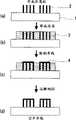
图1(a)到1(f)是说明本发明制备衬底的方法的说明图。图1(a)说明了金属柱的形成;图1(b)说明了金属柱的嵌入;图1(c)说明了穿孔衬底的形成;图1(d)说明芯片安装衬底的形成,图1(e)和1(f)说明了多层衬底的形成。1(a) to 1(f) are explanatory diagrams illustrating a method of preparing a substrate of the present invention. Figure 1(a) illustrates the formation of metal pillars; Figure 1(b) illustrates the embedding of metal pillars; Figure 1(c) illustrates the formation of a through-hole substrate; Figure 1(d) illustrates the formation of a chip mounting substrate, Figures 1(e) and 1(f) illustrate the formation of multilayer substrates.
图2(a)到2(d)是说明制备本发明衬底的方法的关于形成空中布线衬底的说明图。2(a) to 2(d) are explanatory diagrams for forming an air wiring substrate for explaining the method of manufacturing the substrate of the present invention.
图3是在一个例子中在衬底上形成的金属柱的场致发射型扫描电子显微照片(放大率:750倍)。Fig. 3 is a field emission type scanning electron micrograph (magnification: 750 times) of a metal pillar formed on a substrate in one example.
图4是在一个例子中在衬底上形成的金属烧结焊盘的场致发射型扫描电子显微照片(放大率:4000倍)。Fig. 4 is a field emission type scanning electron micrograph (magnification: 4000 times) of a metal sintered pad formed on a substrate in one example.
发明的公开disclosure of invention
根据本发明,提供以下内容:According to the present invention, the following are provided:
(1)制备衬底的方法,包括以下步骤:利用精细喷墨方法在衬底的指定位置上将金属微粒淀积成柱形;然后烧结产物以形成金属柱。(1) A method for preparing a substrate, comprising the steps of: depositing metal particles in a columnar shape on a designated position of the substrate by a fine ink-jet method; and then sintering the product to form a metal column.
(2)根据项目(1)的制备衬底的方法,其中金属柱是突点。(2) The method of producing a substrate according to item (1), wherein the metal post is a bump.
(3)根据项目(1)的制备衬底的方法,其中金属材料填充到在衬底上制作的通孔中,从而形成金属柱。(3) The method of producing a substrate according to item (1), wherein a metal material is filled into a through-hole made on the substrate, thereby forming a metal post.
(4)根据项目(1)的制备衬底的方法,其中金属柱的高度在从10到100μm的范围内。(4) The method of producing a substrate according to item (1), wherein the height of the metal pillar is in the range from 10 to 100 μm.
(5)根据项目(1)或(4)的制备衬底的方法,其中金属柱的底面直径在从0.5到10μm的范围内。(5) The method of producing a substrate according to item (1) or (4), wherein the bottom surface diameter of the metal pillar is in the range from 0.5 to 10 μm.
(6)根据项目(2)的制备衬底的方法,其中突点的底面直径在从0.5到50μm的范围内。(6) The method of producing a substrate according to item (2), wherein the bottom surface diameter of the bumps is in the range from 0.5 to 50 μm.
(7)根据项目(3)的制备衬底的方法,其中通孔的内径在从1到500μm的范围内。(7) The method of producing a substrate according to item (3), wherein the inner diameter of the through hole is in the range from 1 to 500 μm.
(8)根据项目(1)到(7)中任何一个的制备衬底的方法,其中精细喷墨方法是包括喷附精细的液滴、干燥和固化液滴并且依靠电场的集中来堆叠固化的液滴的结构形成方法。(8) The method of preparing a substrate according to any one of items (1) to (7), wherein the fine inkjet method is one comprising spraying fine liquid droplets, drying and solidifying the liquid droplets, and stacking and solidifying by means of concentration of an electric field Droplet structure formation methods.
(9)根据项目(1)到(8)中任何一个的制备衬底的方法,其中金属微粒由从金、银、铜、铂、钯、钨、镍、钽、铋、铅、铟、锡、锌、钛、和铝构成的组中挑选出来的至少一种金属构成。(9) The method for preparing a substrate according to any one of items (1) to (8), wherein the metal particles are made of gold, silver, copper, platinum, palladium, tungsten, nickel, tantalum, bismuth, lead, indium, tin At least one metal selected from the group consisting of , zinc, titanium, and aluminum.
(10)根据项目(1)到(9)中任何一个的制备衬底的方法,其中金属微粒的微粒尺寸在从1到100nm的范围内。(10) The method of producing a substrate according to any one of items (1) to (9), wherein the particle size of the metal fine particles is in the range from 1 to 100 nm.
(11)根据项目(1)到(8)中任何一个的制备衬底的方法,其中金属微粒是平均微粒尺寸在从1到20nm范围内的金微粒,并且按质量包含40%或更多金微粒的悬浮液用作喷射的流体。(11) The method for producing a substrate according to any one of items (1) to (8), wherein the metal microparticles are gold microparticles having an average particle size ranging from 1 to 20 nm and containing 40% or more gold by mass A suspension of microparticles is used as the spray fluid.
(12)根据项目(1)到(8)中任何一个的制备衬底的方法,其中金属微粒是平均微粒尺寸在从1到20nm的范围内的银微粒,并且按质量包含40%或更多银微粒的悬浮液用作喷射的流体。(12) The method for producing a substrate according to any one of items (1) to (8), wherein the metal fine particles are silver fine particles having an average particle size in the range from 1 to 20 nm, and contain 40% by mass or more A suspension of silver particles was used as the spray fluid.
(13)根据项目(1)到(12)中任何一个的制备衬底的方法,其中烧结金属微粒的温度在从150到300℃的范围内。(13) The method of producing a substrate according to any one of items (1) to (12), wherein the temperature for sintering the metal fine particles is in the range from 150 to 300°C.
(14)制作芯片安装衬底的方法,包括以下步骤:在衬底上形成电路;以根据项目(1)、(4)、(5)以及(8)到(13)中任何一个的方法在衬底的指定位置形成金属柱;在衬底上安装构件;以及用树脂密封产物。(14) A method of manufacturing a chip mounting substrate, comprising the steps of: forming a circuit on the substrate; A metal post is formed at a designated position of the substrate; a member is mounted on the substrate; and the product is sealed with a resin.
(15)制作多层衬底的方法,包括以下步骤:在根据项目(14)的方法制作的芯片安装衬底上形成电路;以及重复项目(14)方法中的步骤。(15) A method of producing a multilayer substrate, comprising the steps of: forming a circuit on a chip mounting substrate produced according to the method of item (14); and repeating the steps in the method of item (14).
(16)制作芯片安装衬底的方法,包括以下步骤:在衬底上形成电路;以根据项目(2)、(6)以及(8)到(13)中任何一个的方法在衬底的指定位置形成突点;以及在突点上安装构件。(16) A method of manufacturing a chip mounting substrate, comprising the steps of: forming a circuit on the substrate; forming bumps at the locations; and mounting components on the bumps.
(17)制作多层衬底的方法,包括以下步骤:在衬底上形成电路;在衬底的指定位置中制作通孔;以及通过利用根据项目(3)、(7)以及(8)到(13)中任何一个的方法将金属掩埋到通孔中。(17) A method for producing a multilayer substrate, comprising the steps of: forming a circuit on the substrate; forming a through hole in a designated position of the substrate; The method of any one of (13) buries the metal into the via hole.
(18)衬底,包括利用精细喷墨方法形成的金属柱,所述金属柱通过在衬底的指定位置将金属微粒沉积柱形并且烧结该柱形金属微粒来形成。(18) A substrate comprising metal pillars formed by a fine inkjet method by depositing metal fine particles in a columnar shape at a designated position on the substrate and sintering the cylindrical metal fine particles.
(19)根据项目(18)的衬底,其中金属柱是突点。(19) The substrate according to item (18), wherein the metal post is a bump.
(20)根据项目(18)的衬底,其中金属柱的高度在从10到100μm的范围内。(20) The substrate according to item (18), wherein the height of the metal pillar is in the range from 10 to 100 μm.
(21)根据项目(18)的衬底,其中金属柱的底面直径在从0.5到10μm的范围内。(21) The substrate according to item (18), wherein the base diameter of the metal pillar is in the range from 0.5 to 10 μm.
(22)根据项目(18)的衬底,其中突点的底面直径在从0.5到50μm的范围内。(22) The substrate according to item (18), wherein the bottom surface diameter of the bumps is in the range from 0.5 to 50 µm.
(23)根据项目(18)的衬底,包括在衬底的指定位置形成的金属柱、在形成有金属柱的衬底上安装的构件以及用树脂密封安装有构件的衬底。(23) The substrate according to item (18), including a metal pillar formed at a prescribed position of the substrate, a member mounted on the substrate formed with the metal pillar, and the substrate mounted with the member sealed with a resin.
具体实施方式Detailed ways
通过研究,发明人找出并实现了通过利用能够绘制精细图像的喷墨方法将金属微粒悬浮液喷射到衬底上,并由此在衬底上淀积金属微粒。本发明基于这种发现。Through research, the inventors have found out and realized that the metal particle suspension is sprayed onto a substrate by utilizing an inkjet method capable of drawing fine images, and thus metal particles are deposited on the substrate. The present invention is based on this discovery.
以下将进一步介绍本发明。The present invention will be further described below.
在本发明中,使用电场以使精细的流体液滴飞行并落到衬底上,然后利用精细流体液滴的快速干燥特性和高速固化形成具有大高宽比的精细的三维结构(例如,金属柱和突点)(参见图1(a))。在图1(a)到1(f)中,参考数字1和2分别代表衬底和金属柱。具体地,利用超精细喷喷墨射出精细的液滴。在本发明中的三维结构不仅仅意味着任何二维电路或构图,而是意味着高宽比能够自由地设置且设置为例如3或更大的结构。其形状或许是圆柱体或椭圆柱,并且从上面看其投影形状可以是直线的。三维结构可以是厚度(高度)明显地大于其线宽度(例如,线宽度的3倍或更多)的物品。该结构的例子包括金属柱和突点。In the present invention, an electric field is used to make fine fluid droplets fly and fall on the substrate, and then utilize the fast drying characteristics and high-speed solidification of the fine fluid droplets to form fine three-dimensional structures with large aspect ratios (e.g., metal pillars and bumps) (see Figure 1(a)). In FIGS. 1(a) to 1(f),
能够用在本发明中的精细喷墨装置的例子是电水力(electrohydrodynamic)喷墨装置等,例如,在JP-A-2004-165587中介绍的将指定的波形电压加到其喷嘴端部,以通过静电效应射出微滴。在本发明中的微滴优选直径为20μm或更小,更优选5μm或更小,特别优选1μm或更小,但不限于此。An example of a fine ink-jet device that can be used in the present invention is an electrohydrodynamic ink-jet device or the like, for example, which applies a specified waveform voltage to its nozzle tip as described in JP-A-2004-165587 to Droplets are ejected by electrostatic effect. The microdroplets in the present invention preferably have a diameter of 20 μm or less, more preferably 5 μm or less, particularly preferably 1 μm or less, but not limited thereto.
在本发明中使用的精细喷墨方法使射出小于通过传统的喷墨方法获得的液滴成为可能。当使用这种能够绘制精细图像的喷墨方法喷射出金属微粒悬浮液到衬底上时,通过液滴表面张力的作用、其较大的比表面积的作用以及以液滴的微小为基础的其它效应,涂覆的金属微粒悬浮液中的溶剂瞬间从悬浮液中蒸发。结果,金属微粒附着于衬底上。换句话说,本发明通过使用精细喷墨方法喷涂超精细液滴以及干燥和固化液滴形成三维结构。(在本发明中,用语“干燥和固化”的意思是对象蒸发和变干,从而使对象本身的粘稠度以对象至少能够堆叠的方式变高。)此外,适当地控制,例如,碰撞能量、电场的集中以及衬底的温度或其气氛等条件,借此形成具有高度的结构。因此,根据本发明的制备方法,在射出液滴的间隔之间不必采用其它固化液滴的步骤。因此,连续地实现精细液滴的射出和堆叠,由此能够有效地制作具有金属柱的衬底。The fine inkjet method used in the present invention makes it possible to shoot liquid droplets smaller than those obtained by conventional inkjet methods. When using this inkjet method capable of drawing fine images to eject the suspension of metal particles onto the substrate, through the effect of the surface tension of the droplet, the effect of its large specific surface area, and other factors based on the smallness of the droplet effect, the solvent in the coated metal particle suspension evaporates instantaneously from the suspension. As a result, metal particles are attached to the substrate. In other words, the present invention forms a three-dimensional structure by spraying ultrafine liquid droplets using a fine inkjet method and drying and solidifying the liquid droplets. (In the present invention, the term "drying and curing" means that the object evaporates and becomes dry so that the viscosity of the object itself becomes high in such a way that the object can at least be stacked.) In addition, appropriately controlling, for example, the collision energy , the concentration of the electric field and the temperature of the substrate or its atmosphere and other conditions, thereby forming a structure with a high degree. Therefore, according to the production method of the present invention, it is not necessary to employ other steps of solidifying the droplets between the intervals between ejecting the droplets. Therefore, ejection and stacking of fine liquid droplets are continuously achieved, whereby a substrate with metal pillars can be efficiently fabricated.
此外,在依靠所加电场作用的超精细喷墨中,指向喷嘴顶端的应力不断地作用在由固化之前附着的液滴(在下文中称作“之前着陆的液滴”)形成的结构的端部。因此,结构能够生长同时被拉向喷嘴。因此,即使结构具有大高宽比也能够生长而不会倒塌。当结构开始生长时,电场可以聚焦在其生长点。因此,能够确定和精确地引导射出的液滴着陆到由之前附着的液滴构成的结构上。因此,能够有效地促进结构的生长。可以以能够获得上述作用的方式适当地设置结构生长的条件,由液滴流体的特性等决定。例如,可以使用在日本专利申请No.2004-221937和日本专利申请No.2004-221986中介绍的条件。Furthermore, in ultra-fine inkjet that relies on the action of an applied electric field, stress directed toward the tip of the nozzle continuously acts on the end of a structure formed by droplets attached before solidification (hereinafter referred to as "previously landed droplets") . Thus, the structure can grow while being pulled towards the nozzle. Therefore, even structures with large aspect ratios can grow without collapsing. When the structure begins to grow, the electric field can be focused at the point of its growth. Thus, it is possible to define and precisely guide the landing of the ejected droplet onto the structure formed by the previously attached droplet. Therefore, the growth of the structure can be effectively promoted. Conditions for structure growth may be appropriately set in such a manner that the above-described effects can be obtained, determined by the characteristics of the droplet fluid and the like. For example, the conditions described in Japanese Patent Application No. 2004-221937 and Japanese Patent Application No. 2004-221986 can be used.
通过本发明的方法形成的结构的高宽比没有特别限制,并且优选1或更多,更优选2或更多,更加优选3或更多,特别优选5或更多。高宽比没有上限。如果三维结构能够独自立起来,则结构可以以其高宽比将是100或更多、或者200或更多的方式无限地生长。The aspect ratio of the structure formed by the method of the present invention is not particularly limited, and is preferably 1 or more, more preferably 2 or more, still more preferably 3 or more, particularly preferably 5 or more. There is no upper limit to the aspect ratio. If the three-dimensional structure could stand on its own, the structure could grow infinitely in such a way that its aspect ratio would be 100 or more, or 200 or more.
用在本发明中的在金属微粒膏中的金属种类的例子是几乎所有种类的金属或者其氧化物。优选金属是具有导电性的金属,例如,金、银、铜、铂、钯、钨、钽、铋、铅、锡、铟、锌、钛、镍、铁、钴、铝等。更优选的金属是金、银、铜、铂或钯。特别优选的金属是金或银。可以使用单一的金属,或者可以使用由两种或更多种金属制成的合金。金属微粒(在下文中可以称作“金属纳米微粒”)的颗粒尺寸优选从1到100nm,更优选从1到20nm,更加优选从2到10nm。Examples of metal species in the metal particle paste used in the present invention are almost all kinds of metals or oxides thereof. The metal is preferably a conductive metal such as gold, silver, copper, platinum, palladium, tungsten, tantalum, bismuth, lead, tin, indium, zinc, titanium, nickel, iron, cobalt, aluminum and the like. More preferred metals are gold, silver, copper, platinum or palladium. Particularly preferred metals are gold or silver. A single metal may be used, or an alloy of two or more metals may be used. The particle size of the metal fine particles (may be referred to as "metal nanoparticles" hereinafter) is preferably from 1 to 100 nm, more preferably from 1 to 20 nm, still more preferably from 2 to 10 nm.
因为喷射出的金属微粒悬浮液(在下文中称作“金属微粒膏”)的液滴、由着陆的金属微粒悬浮液的液滴形成的金属柱的底面直径(或横截面直径)是小的,所以能够制作非常小的金属柱(在下文中称作“金属微粒层”)。金属微粒层的直径优选从0.01到10μm,更优选从0.5到10μm,更加优选从0.5到5μm。通过不断喷射悬浮液,淀积每个具有这种非常小的面积的金属微粒层,并且在垂直方向(高度方向)上堆叠,以便制作由金属微粒制成的圆柱淀积层。圆柱淀积层的高度优选从0.1到500μm,更优选从1到100μm,特别优选从10到100μm。Since the ejected droplets of the metal particle suspension (hereinafter referred to as "metal particle paste"), the base diameter (or cross-sectional diameter) of the metal pillars formed by the droplets of the metal particle suspension that landed are small, It is therefore possible to fabricate very small metal pillars (hereinafter referred to as "metal particle layer"). The diameter of the metal particle layer is preferably from 0.01 to 10 μm, more preferably from 0.5 to 10 μm, still more preferably from 0.5 to 5 μm. Metal particle layers each having such a very small area are deposited by continuously spraying the suspension, and stacked in the vertical direction (height direction) to make cylindrical deposited layers made of metal particles. The height of the cylindrically deposited layer is preferably from 0.1 to 500 μm, more preferably from 1 to 100 μm, particularly preferably from 10 to 100 μm.
在本发明中使用的金属微粒膏的溶剂根据散布方式分为水溶剂和有机溶剂。有机溶剂可以更进一步分为主要由极性溶剂构成的溶剂和主要由非极性溶剂构成的溶剂。溶剂可以由混合物组成。Solvents for the metal fine particle paste used in the present invention are classified into aqueous solvents and organic solvents according to the method of spreading. Organic solvents can be further classified into solvents mainly composed of polar solvents and solvents mainly composed of nonpolar solvents. Solvents can consist of mixtures.
在本发明中使用的金属微粒膏的溶剂可以是水、十四烷、甲苯、和醇类等。在悬浮液或膏中的金属微粒的浓度希望更高,并且优选按质量为40%或更多,更优选按质量为45%或更多。在这方面,由于以下理由:例如,在溶剂的沸点较低的情况下,当液滴飞行或着陆时溶剂成分蒸发,考虑溶剂的流动性、蒸汽压、沸点和其它特性以及形成三维结构的条件,例如,衬底的温度和/或气氛、蒸汽压和射出液滴的量,可以决定浓度。The solvent of the metal particle paste used in the present invention may be water, tetradecane, toluene, alcohols and the like. The concentration of the fine metal particles in the suspension or paste is desirably higher, and is preferably 40% by mass or more, more preferably 45% by mass or more. In this regard, for the following reasons: For example, in the case of a solvent with a low boiling point, the solvent component evaporates when the droplet flies or lands, considering the fluidity, vapor pressure, boiling point and other characteristics of the solvent and the conditions for forming a three-dimensional structure For example, the temperature and/or atmosphere of the substrate, the vapor pressure and the volume of the ejected droplet can determine the concentration.
为了形成三维结构,最好在本发明中使用的金属微粒膏的粘稠度较高。然而,粘稠度必须在膏可以喷射的范围之内。因此,必须精心确定粘稠度。粘稠度也取决于膏的种类。例如,在银纳米膏的情况下,粘稠度优选3到50厘泊(更优选从8到15厘泊)。在陶瓷溶胶-凝胶液体的情况下,虽然溶液的粘稠度相当低也可以得到良好外形的柱状构造。这是因为溶剂的沸点较低,因此溶剂在液滴飞行或着陆的时候蒸发,从而粘稠度突然变高。In order to form a three-dimensional structure, it is preferable that the metal particle paste used in the present invention has a high viscosity. However, the consistency must be within the range in which the paste can be sprayed. Therefore, the viscosity must be carefully determined. The consistency also depends on the type of paste. For example, in the case of silver nanopaste, the viscosity is preferably from 3 to 50 centipoise (more preferably from 8 to 15 centipoise). In the case of ceramic sol-gel liquids, columnar structures of good shape can be obtained although the viscosity of the solution is rather low. This is because the boiling point of the solvent is low, so the solvent evaporates when the droplet flies or lands, and the viscosity suddenly becomes higher.
在圆柱淀积层形成之后,通过在低温下加热烧结该层,借此熔化微粒并且彼此粘附,从而形成圆柱金属层。最好根据所使用金属或合金的特性,例如,其熔点,适当地设置烧结温度。温度优选从100到500℃,更优选从150到300℃。在烧结时的气氛可以是空气、惰性气氛、减压气氛、还原性气氛,例如,氢等。为了防止金属超精细微粒被氧化,优选还原性气氛。After the cylindrical deposition layer is formed, the layer is sintered by heating at a low temperature, whereby particles are melted and adhered to each other, thereby forming a cylindrical metal layer. It is preferable to appropriately set the sintering temperature according to the properties of the metal or alloy used, for example, its melting point. The temperature is preferably from 100 to 500°C, more preferably from 150 to 300°C. The atmosphere at the time of sintering may be air, an inert atmosphere, a reduced pressure atmosphere, a reducing atmosphere such as hydrogen or the like. In order to prevent the metal ultrafine particles from being oxidized, a reducing atmosphere is preferable.
因为这样形成的金属柱按百分比具有高金属含量并且具有精细坚固的结构,所以柱显示出接近金属本身的体电阻率的值,因此可以得到0.1×10⁻⁵Ω·cm或更小的低电阻。Because the metal pillars thus formed have a high metal content by percentage and have a fine and strong structure, the pillars show a value close to the volume resistivity of the metal itself, and thus a low resistance of 0.1×10⁻⁵ Ω·cm or less can be obtained .
金属微粒的使用使在形成、烧结和固定三维结构之后能够用例如溶于有机溶剂中的树脂掩埋结构(金属柱)(参见图1(b))。在图1(a)到1(f)中,参考数字3代表涂层树脂。换句话说,在由树脂材料制成结构的情况下,依赖于树脂与有机溶剂的组合,结构将被溶剂侵蚀,从而破坏结构本身;然而,在用金属微粒形成结构的情况下,通过烧结结构使得结构能够稳定地抵抗所使用的有机溶剂等等。因此,通过在用树脂等掩埋结构之后仅仅腐蚀和溶解金属形成穿孔衬底(参见图1(c))。例如,对于金属的溶解,可以使用硝酸铁溶液或铬酐和浓硫酸的混合溶液。The use of metal microparticles enables to bury the structure (metal post) with, for example, a resin dissolved in an organic solvent after forming, sintering, and fixing the three-dimensional structure (see FIG. 1( b )). In Figs. 1(a) to 1(f),
通过在形成金属柱的衬底上安装芯片,并且用树脂密封产物,从而可以制作在其上部形成有导电区的芯片安装衬底(图1(d))。By mounting a chip on a substrate on which metal pillars are formed, and sealing the product with a resin, a chip mounting substrate having a conductive region formed thereon can be manufactured (FIG. 1(d)).
在图1(a)到1(f)中,参考数字4代表电路布线。此时使用的密封树脂优选热固性树脂或紫外线固化树脂,例如,环氧树脂、酚醛树脂或丙烯酸树脂。In FIGS. 1(a) to 1(f), reference numeral 4 denotes circuit wiring. The sealing resin used at this time is preferably a thermosetting resin or an ultraviolet curing resin, for example, epoxy resin, phenolic resin, or acrylic resin.
此外,通过在这种芯片安装衬底上形成电路,并且用树脂密封产物,借此可以形成在其上部形成有导电区的多层衬底(参见图1(e)和1(f))。在图1(a)到1(f)中,参考数字5和6分别代表金属柱和树脂(涂层树脂)。通过使用金属微粒膏的丝网印刷方法、喷墨方法和转印法中的任何一个可以实现电路的形成。此时使用的金属微粒膏优选与用来淀积金属柱的金属膏种类相同。然而,可以适当地使用不同金属种类的膏。最好设置金属微粒膏的粘稠度以及其它物理特性适合于电路形成或淀积。Furthermore, by forming a circuit on such a chip mounting substrate and sealing the product with a resin, a multilayer substrate having a conductive region formed thereon can be formed (see FIGS. 1(e) and 1(f)). In FIGS. 1( a ) to 1 ( f ), reference numerals 5 and 6 denote a metal post and a resin (coating resin), respectively. Formation of a circuit can be achieved by any one of a screen printing method using a metal particle paste, an inkjet method, and a transfer method. The metal particle paste used at this time is preferably the same kind as the metal paste used to deposit the metal pillars. However, pastes of different metal species may be suitably used. The viscosity and other physical properties of the metal particle paste are preferably set to be suitable for circuit formation or deposition.
此外,在衬底上形成金属柱并用树脂掩埋,然后在衬底上形成电路之后,可以仅仅腐蚀和除去树脂,借此可以形成具有空中布线(低-K布线)的衬底(参见图2(a)到2(d))。在图2(a)到2(d)中,参考数字1、2、3和4分别代表衬底、金属柱、涂层树脂和电路布线。在这种情况下使用的树脂优选热固性树脂。可以使用多种树脂,只要树脂是可溶解的。In addition, after metal pillars are formed on the substrate and buried with resin, and then circuits are formed on the substrate, only the resin can be etched and removed, whereby a substrate with aerial wiring (low-K wiring) can be formed (see FIG. 2( a) to 2(d)). In FIGS. 2(a) to 2(d),
以与上述相同的方式,可以在衬底上形成突点。具体地,可以利用基于所述同样的喷墨方法的精细印刷工艺的优点以圆锥体的形式淀积金属微粒悬浮液,由此在要求的位置形成具有要求尺寸的金属锥体。可以在低温下烧结,以使微粒熔化并彼此粘附,借此可以形成突点。In the same manner as above, bumps can be formed on the substrate. Specifically, the metal particle suspension can be deposited in the form of cones by taking advantage of the fine printing process based on the same inkjet method, thereby forming metal cones with desired dimensions at desired locations. Sintering can be performed at low temperatures to melt the particles and adhere to each other, whereby bumps can be formed.
形成突点的底面直径优选从0.01到100μm,更优选从0.5到50μm,更加优选从1到50μm,突点的高度优选从0.1到500μm,更优选从1到100μm。形成的突点显示出接近金属本身体电阻率的低电阻;因此,通过在突点上安装精细芯片,可以制作精细芯片安装衬底。The diameter of the bottom surface where the bumps are formed is preferably from 0.01 to 100 μm, more preferably from 0.5 to 50 μm, still more preferably from 1 to 50 μm, and the height of the bumps is preferably from 0.1 to 500 μm, more preferably from 1 to 100 μm. The formed bumps exhibit low resistance close to the bulk resistivity of the metal itself; therefore, by mounting fine chips on the bumps, fine chip mounting substrates can be produced.
以与上述相同的方式,可以将金属填充到衬底中的通孔中。具体地,以如上所述相同的喷墨方法为基础的精细印刷方法可用于在衬底中制造的通孔中嵌入金属微粒膏。可以烧结来熔化和粘附每个微粒,借此金属可以填充到通孔中。In the same manner as above, metal can be filled into the via holes in the substrate. Specifically, a fine printing method based on the same inkjet method as described above can be used to embed metal particle paste in via holes made in a substrate. Sintering can be used to melt and adhere each particle, whereby the metal can fill the vias.
可以在本发明中使用的通孔的内径优选从1到500μm,更优选从5到300μm,特别优选从20到200μm。其深度优选从5到2000μm,更优选从10到1000μm。可以通过激光穿孔方法、机械穿孔方法、蚀刻等制造通孔。The inner diameter of the through-holes that can be used in the present invention is preferably from 1 to 500 μm, more preferably from 5 to 300 μm, particularly preferably from 20 to 200 μm. Its depth is preferably from 5 to 2000 μm, more preferably from 10 to 1000 μm. The via hole may be produced by a laser perforation method, a mechanical perforation method, etching, or the like.
填充到通孔中的金属具有接近金属本身体电阻率的低电阻。其后,可以在衬底上安装构件,可以制作安装芯片的多层衬底。The metal filled into the via has a low resistance close to the bulk resistivity of the metal itself. Thereafter, components can be mounted on the substrate, and a multilayer substrate on which chips are mounted can be fabricated.
根据本发明,使用能够绘制精细图像的喷墨式印刷方法喷射、淀积和堆叠金属微粒悬浮液到衬底上,借此可以提供其上形成有精细金属柱的衬底。According to the present invention, a metal particle suspension is jetted, deposited, and stacked onto a substrate using an inkjet printing method capable of drawing fine images, whereby a substrate on which fine metal pillars are formed can be provided.
根据本发明制备衬底的方法,能够容易地制作通过任何常规方法基本上不能实现的具有大高宽比(结构的高度与结构底面的最短直径的比(高度/底面的最短直径))结构的衬底。According to the method for preparing a substrate of the present invention, it is possible to easily manufacture structures with a large aspect ratio (the ratio of the height of the structure to the shortest diameter of the bottom surface of the structure (the shortest diameter of the height/bottom surface)) that cannot be realized by any conventional method. substrate.
在衬底中通过本发明的方法制作的精细的金属柱或突点按百分比具有较高的金属含量,并且具有精细坚固的结构,从而显示出接近金属本身的体电阻率的电阻值。使用这种金属柱或突点的芯片安装衬底、多层衬底或穿孔衬底表现出其电阻值较低的出色效果。The fine metal pillars or bumps produced by the method of the present invention in the substrate have relatively high metal content by percentage, and have a fine and firm structure, thereby showing a resistance value close to the volume resistivity of the metal itself. A chip mounting substrate, a multilayer substrate, or a through-hole substrate using such metal pillars or bumps exhibits an excellent effect that its resistance value is low.
以下以给出的例子为基础更详细地介绍本发明,但是发明并不以这些为限制。The invention is described in more detail below on the basis of given examples, but the invention is not restricted thereto.
例子example
(例子1到3,以及比较例1)(Examples 1 to 3, and Comparative Example 1)
在例1到3的每个中,制备显示出适合于喷墨式印刷方法的液体粘度并且包含银纳米微粒作为导电介质的膏状悬浮液。In each of Examples 1 to 3, a paste-like suspension exhibiting a liquid viscosity suitable for an inkjet printing method and containing silver nanoparticles as a conductive medium was prepared.
使用以下银纳米微粒的原料:市场上可买到的超精细银微粒悬浮液(商品名:Independently Dispersed Ultra-Fine Particles Ag1T,由Vacuum Metallurgical Co.,Ltd.制造),具体地,平均颗粒尺寸3nm的银微粒悬浮液包括按质量35份的微粒,按质量7份的十二烷胺(分子量:185.36,熔点:28.3℃,沸点:248℃,以及密度(d440):0.7841)作为烷基胺,以及按质量58份的甲苯作为有机溶剂。银微粒悬浮液的液体粘度为1mPa·s(在20℃)。The following raw material of silver nanoparticles was used: a commercially available ultrafine silver particle suspension (trade name: Independently Dispersed Ultra-Fine Particles Ag1T, manufactured by Vacuum Metallurgical Co., Ltd.), specifically, an average particle size of 3 nm The silver microparticle suspension includes 35 parts by mass of microparticles, 7 parts by mass of dodecylamine (molecular weight: 185.36, melting point: 28.3°C, boiling point: 248°C, and density (d440): 0.7841) as an alkylamine, And 58 parts by mass of toluene as an organic solvent. The liquid viscosity of the silver particle suspension was 1 mPa·s (at 20° C.).
在1L茄形烧瓶中,首先加入5.8g十二烷胺并且与500g银微粒悬浮液(按质量包含35%的银)混合。混合物在80℃下加热并搅拌1小时。在搅拌结束之后,通过减压浓缩除去银微粒悬浮液中包含的悬浮溶剂甲苯。In a 1 L eggplant-shaped flask, 5.8 g of dodecylamine were first added and mixed with 500 g of a silver particle suspension (containing 35% silver by mass). The mixture was heated and stirred at 80°C for 1 hour. After the stirring was completed, the suspension solvent toluene contained in the silver microparticle suspension was removed by concentration under reduced pressure.
在除去溶剂的混合物中在按质量包含银微粒的每175份中以表1所示的数量加入十四烷(商品名:N14,由Nikko Petrochemicals Co.,Ltd.制造,粘稠度:2.0到2.3mPa·s(20℃),熔点:5.86℃,沸点:253.57℃,密度(d420):0.7924)。在室温下(25℃)搅拌混合物,从而制备同质的悬浮液。在搅拌结束之后,用0.2μm的薄膜滤器过滤悬浮液。得到的例1到3和比较例1的每个悬浮液是高度流体膏形式的同质的和深蓝色银纳米微粒悬浮液(银纳米微粒油墨)。Tetradecane (trade name: N14, manufactured by Nikko Petrochemicals Co., Ltd., viscosity: 2.0 to 2.3mPa·s (20°C), melting point: 5.86°C, boiling point: 253.57°C, density (d420): 0.7924). The mixture was stirred at room temperature (25°C) to prepare a homogeneous suspension. After the stirring was complete, the suspension was filtered with a 0.2 μm membrane filter. Each suspension of Examples 1 to 3 and Comparative Example 1 was obtained as a homogeneous and dark blue silver nanoparticle suspension (silver nanoparticle ink) in the form of a highly fluid paste.
表1显示出在得到的银纳米微粒悬浮液(银纳米微粒油墨)的每一个中包含的成分数量及其液体粘度(在20℃下用B型旋转粘度计测量)。Table 1 shows the amounts of ingredients contained in each of the obtained silver nanoparticle suspensions (silver nanoparticle inks) and their liquid viscosities (measured with a B-type rotational viscometer at 20° C.).
为了参考,整体的银单体显示出10.49g·cm-3(在20℃下)的密度和1.59μΩ·cm(在20℃下)的电阻率。在此提到的银微粒的平均粒度直径是3nm。For reference, the bulk silver monomer exhibits a density of 10.49 g·cm−3 (at 20° C.) and a resistivity of 1.59 μΩ·cm (at 20° C.). The mean particle size diameter of the silver fine particles mentioned here is 3 nm.
表1Table 1
制作的银纳米微粒悬浮液(银纳米微粒油墨)的成分和特性
表2Table 2
银纳米微粒悬浮液(银纳米微粒油墨)的应用特性和得到的烧结体的评估结果
采用超精细流体喷射装置(超精细喷墨装置)用得到的银纳米微粒悬浮液分别在玻璃上绘制直径5μm图样的图像。此时,在超精细喷墨装置中构成的喷口的孔径选为0.6μm,并且使喷射出的液滴量具有相同的值。用银纳米微粒悬浮液的每一个液滴绘制的点的直径为表2中所示的值。The resulting silver nanoparticle suspension was used to draw images of patterns with a diameter of 5 μm on glass, respectively, using an ultrafine fluid jetting device (ultrafine inkjet device). At this time, the diameter of the orifice formed in the ultra-fine inkjet device was selected to be 0.6 μm, and the ejected droplet volume was made to have the same value. The diameters of the dots plotted with each droplet of the silver nanoparticle suspension are the values shown in Table 2.
在该绘制条件下,通过喷墨方法分别涂覆油墨,从而形成点状图样,其中墨点之间的间隔是相同的,然后以与上述相同的点状图样彼此重叠的方式反复涂覆。这样,制作具有表2所示总叠层高度的圆柱形银纳米颗粒涂层(参见图1(a))。Under this drawing condition, ink is applied separately by an inkjet method to form a dot pattern in which the intervals between ink dots are the same, and then the coating is repeated in such a manner that the same dot patterns as described above overlap each other. In this way, a cylindrical silver nanoparticle coating was produced with the total stack height shown in Table 2 (see FIG. 1( a )).
当分别使用例1到3的银纳米微粒悬浮液时,在各涂覆操作之间的时间期间,进行在涂覆的薄层中包含的悬浮溶剂的蒸发。结果,涂覆的薄层处于粘性状态。另一方面,当使用比较例1的银纳米微粒悬浮液时,在各涂覆操作之间的时间期间在涂覆的薄层中包含的悬浮溶剂也蒸发,但是涂覆的薄层处于流态。When using the silver nanoparticle suspensions of Examples 1 to 3, respectively, during the time between the respective coating operations, evaporation of the suspension solvent contained in the coated thin layers took place. As a result, the coated thin layer is in a sticky state. On the other hand, when the silver nanoparticle suspension of Comparative Example 1 was used, the suspension solvent contained in the coated thin layer was also evaporated during the time between each coating operation, but the coated thin layer was in a fluid state .
在绘制之后,在玻璃上的银纳米微粒涂层在240℃下经受1小时的热处理,从而燃烧。这样,形成银纳米微粒的烧结体层。用超级深度彩色3D形状测量显微镜(商品名:VK-9500,由Keyence Co.制造)测量得到的烧结体层圆形底面的直径和烧结体层的高度(厚度)。After drawing, the silver nanoparticle coating on the glass was subjected to heat treatment at 240° C. for 1 hour to burn. In this way, a sintered body layer of silver nanoparticles was formed. The diameter of the circular bottom surface of the sintered body layer and the height (thickness) of the sintered body layer were measured with a super deep color 3D shape measuring microscope (trade name: VK-9500, manufactured by Keyence Co.).
表2显示出了以下评估结果:用一个液滴绘制的点的直径;得到的烧结体层的圆形底面的直径;以及烧结体层的高度(厚度)。此外,图3示出了借助于放大750倍的场致发射型扫描电子显微镜(商品名:JSM-6340F,由JEOL Ltd.制造),通过观察根据上述生产过程使用例1的银纳米微粒悬浮液形成的烧结金属列的外部形状得到的印出图像。Table 2 shows the evaluation results of: the diameter of a dot drawn with one droplet; the diameter of the circular bottom surface of the resulting sintered body layer; and the height (thickness) of the sintered body layer. In addition, Fig. 3 shows by means of a field emission type scanning electron microscope (trade name: JSM-6340F, manufactured by JEOL Ltd.) magnified 750 times, by observing the silver nanoparticle suspension using Example 1 according to the above-mentioned production process The outer shape of the formed sintered metal columns results in a printed image.
单独地,在上述喷墨叠层涂覆条件下,在滑动玻璃上使用得到的银纳米微粒悬浮液印刷10mm×50mm(宽度方向上)的图样;从而在涂覆叠层时制作平均10μm的膜厚度。在印刷之后,在滑动玻璃上的纳米微粒油墨叠层涂层在240℃下受到1小时的热处理,从而燃烧包含银纳米微粒的涂层。这样,形成由银纳米微粒烧结体层制成的导电体层图样。关于使用例1到3和比较例1的银纳米微粒悬浮液形成的矩形膜形电导体层,每个层被认为是具有层的平均膜厚度的同质电导体层,并且测量其体电阻率。在表2中也示出了体电阻率的测量结果。Separately, a pattern of 10 mm x 50 mm (in the width direction) was printed using the resulting silver nanoparticle suspension on a slide glass under the inkjet stack coating conditions described above; thereby producing an average 10 μm film when coating the stack thickness. After printing, the nanoparticle ink stack coating on the slide glass was subjected to a heat treatment at 240° C. for 1 hour to burn the silver nanoparticle-containing coating. In this way, a conductor layer pattern made of a silver nanoparticle sintered body layer was formed. Regarding the rectangular film-shaped electrical conductor layers formed using the silver nanoparticle suspensions of Examples 1 to 3 and Comparative Example 1, each layer was considered as a homogeneous electrical conductor layer having an average film thickness of the layer, and the volume resistivity thereof was measured . In Table 2, the measurement results of the volume resistivity are also shown.
(例4和5,以及比较例2)(Examples 4 and 5, and Comparative Example 2)
在例4和5的每个中,制备显示出适合于精细喷墨印刷方法的液体粘度并且包含银纳米微粒作为导电介质的膏状悬浮液。In each of Examples 4 and 5, a paste-like suspension exhibiting a liquid viscosity suitable for a fine inkjet printing method and containing silver nanoparticles as a conductive medium was prepared.
在1L茄形烧瓶中,加入87.5g(固体银质量的50%)2-乙基己胺(由Tokyo Kasei制造,沸点:169℃)和52.5g(固体银质量的30%)二丙二醇,并且与500g的银微粒悬浮液Ag1T(按质量包含35%的银,并且由Vacuum Metallurgical Co.,Ltd.制造)混合。混合物在80℃下加热并搅拌1小时。在搅拌结束之后,通过减压浓缩除去Ag1T中包含的悬浮溶剂甲苯。In a 1 L eggplant-shaped flask, 87.5 g (50% of the mass of solid silver) of 2-ethylhexylamine (manufactured by Tokyo Kasei, boiling point: 169° C.) and 52.5 g (30% of the mass of solid silver) of dipropylene glycol were charged, and Mixed with 500 g of silver particle suspension Ag1T (containing 35% silver by mass and manufactured by Vacuum Metallurgical Co., Ltd.). The mixture was heated and stirred at 80°C for 1 hour. After the stirring was completed, the suspension solvent toluene contained in Ag1T was removed by concentration under reduced pressure.
除去溶剂的混合物转移到2L大口杯中,然后加入1000g极性溶剂丙酮。混合物在室温下搅拌3分钟,然后搁置不动。在该处理中,当加入极性溶剂丙酮和搅拌产物并且搁置不动时,银纳米微粒沉淀在大口杯底部上。在混合物中包含的不必要的有机成分溶于上层清液中,制作褐色丙酮溶液。除去上层清液,然后沉淀中再次加入800g丙酮。搅拌得到的溶液并搁置不动,以沉淀银纳米微粒。尔后,除去上层清液的丙酮溶液层。当观察到上层清液丙酮层的颜色状态时,沉淀中进一步加入500g丙酮,以重复相同的操作。接下来,300g丙酮加到上述步骤生成的沉淀中,然后搅拌溶液并搁置不动。此时,用肉眼观看上层清液丙酮层。没有发现颜色。The solvent-free mixture was transferred to a 2L beaker, and 1000 g of polar solvent acetone was added. The mixture was stirred at room temperature for 3 minutes, then set aside. During this treatment, silver nanoparticles precipitated on the bottom of the beaker when the polar solvent acetone was added and the product was stirred and left untouched. Unnecessary organic components contained in the mixture were dissolved in the supernatant to make a brown acetone solution. Remove the supernatant, and then add 800 g of acetone again to the precipitate. The resulting solution was stirred and left undisturbed to precipitate the silver nanoparticles. Thereafter, the acetone solution layer of the supernatant was removed. When the color state of the supernatant acetone layer was observed, 500 g of acetone was further added to the precipitate to repeat the same operation. Next, 300 g of acetone was added to the precipitate formed in the above step, and the solution was stirred and left to stand. At this time, the supernatant acetone layer was observed with the naked eye. No color was found.
除去该上层清液丙酮层,随后蒸发在大口杯底部上的银纳米微粒沉淀中剩余的丙酮溶剂,以干燥微粒。结果,生成蓝色细粉末。The supernatant acetone layer was removed, followed by evaporation of the remaining acetone solvent in the silver nanoparticle precipitate on the bottom of the beaker to dry the particles. As a result, a blue fine powder was produced.
向得到的蓝色细粉末中对按质量每175份所包含的银微粒,以表3中示出的各个量加入十四烷(商品名:N14,由Nikko PetrochemicalsCo.,Ltd.制造,熔点:5.86℃,沸点253.57℃)。此外,混合物中加入23.4g双-2-乙基己胺(Tokyo Kasei制造(沸点263℃))和300g己烷,然后在70℃下混合物加热和搅拌30分钟。通过该加热和搅拌,蓝色细粉末形式的银纳米微粒再次散开,生成同质的悬浮液。在搅拌结束之后,用0.2μm的薄膜滤器过滤悬浮液。其后,通过减压浓缩除去滤出液中的己烷。得到的例4和5以及比较例2的每个悬浮液是高度流体膏形式的同质的深蓝色银纳米微粒悬浮液(银纳米微粒油墨)。To the obtained blue fine powder, tetradecane (trade name: N14, manufactured by Nikko Petrochemicals Co., Ltd., melting point: 5.86°C, boiling point 253.57°C). Further, 23.4 g of bis-2-ethylhexylamine (manufactured by Tokyo Kasei (boiling point 263°C)) and 300 g of hexane were added to the mixture, and then the mixture was heated and stirred at 70°C for 30 minutes. By this heating and stirring, the silver nanoparticles in the form of a fine blue powder are dispersed again, resulting in a homogeneous suspension. After the stirring was complete, the suspension was filtered with a 0.2 μm membrane filter. Thereafter, hexane in the filtrate was removed by concentration under reduced pressure. Each of the resulting suspensions of Examples 4 and 5 and Comparative Example 2 was a homogeneous dark blue silver nanoparticle suspension (silver nanoparticle ink) in the form of a highly fluid paste.
表3显示出在得到的各银纳米微粒悬浮液(银纳米微粒油墨)中包含的成分数量及其液体粘度(在20℃下用B型旋转粘度计测量)。用于参考,整体的银单体显示出10.50g·cm-3(在20℃下)的密度和1.59μΩ·cm(在20℃下)的电阻率。在此提到的银微粒的平均粒度直径是3nm。Table 3 shows the amounts of ingredients contained in each of the obtained silver nanoparticle suspensions (silver nanoparticle inks) and their liquid viscosities (measured with a B-type rotational viscometer at 20° C.). For reference, the bulk silver monomer exhibits a density of 10.50 g·cm−3 (at 20° C.) and a resistivity of 1.59 μΩ·cm (at 20° C.). The mean particle size diameter of the silver fine particles mentioned here is 3 nm.
表3table 3
制作的银纳米微粒悬浮液(银纳米微粒油墨)的成分和特性
表4Table 4
银纳米微粒悬浮液(银纳米微粒油墨)的应用特性和得到的烧结体的评估结果
用超精细流体喷射装置(超精细喷墨装置)用得到的银纳米微粒悬浮液分别在玻璃上绘制直径2.5μm图样的图像。此时,在超精细喷墨装置中构成的喷口的孔径选择为0.6μm,并且使喷射出的液滴量具有相同的值。用银纳米微粒悬浮液的每一个液滴绘制的点的直径为表4中所示的值。在该绘制条件下,通过喷墨方法分别涂覆油墨,从而形成点状图样,其中墨点之间的间隔是相同的,然后以与上述相同的点状图样彼此重叠的方式反复涂覆。这样,制作具有表4所示总叠层高度的圆柱形银纳米微粒涂层。The obtained silver nanoparticle suspensions were respectively used to draw images of patterns with a diameter of 2.5 μm on glass using a microfine fluid ejection device (microjet device). At this time, the diameter of the orifice formed in the ultra-fine inkjet device is selected to be 0.6 μm, and the ejected droplet volume has the same value. The diameters of the dots plotted with each droplet of the silver nanoparticle suspension are the values shown in Table 4. Under this drawing condition, ink is applied separately by an inkjet method to form a dot pattern in which the intervals between ink dots are the same, and then the coating is repeated in such a manner that the same dot patterns as described above overlap each other. In this way, a cylindrical silver nanoparticle coating having the total stack height shown in Table 4 was produced.
当分别使用例4和5的银纳米微粒悬浮液时,在各涂覆操作之间的时间期间,进行在涂覆的薄层中包含的悬浮溶剂的蒸发。结果,涂覆的薄层处于粘性状态。另一方面,当使用比较例2的银纳米微粒悬浮液时,在各涂覆操作之间的时间期间在涂覆的薄层中包含的悬浮溶剂也蒸发,但是涂覆的薄层处于流态。When using the silver nanoparticle suspensions of Examples 4 and 5, respectively, during the time between the respective coating operations, evaporation of the suspension solvent contained in the applied thin layers took place. As a result, the coated thin layer is in a sticky state. On the other hand, when the silver nanoparticle suspension of Comparative Example 2 was used, the suspension solvent contained in the coated thin layer was also evaporated during the time between each coating operation, but the coated thin layer was in a fluid state .
在绘制之后,在玻璃上的银纳米微粒涂层在240℃下经受1小时的热处理,从而燃烧。这样,形成银纳米微粒的烧结体层。After drawing, the silver nanoparticle coating on the glass was subjected to heat treatment at 240° C. for 1 hour to burn. In this way, a sintered body layer of silver nanoparticles was formed.
分别通过显微镜观察测量得到的烧结体层的圆形底面的直径和烧结体层的高度(厚度)。表4显示出了以下评估结果:用来自液滴中的一个液滴绘制的点的直径;得到的烧结体层的圆形底面的直径;以及烧结体层的高度(厚度)。The diameter of the circular bottom surface of the obtained sintered body layer and the height (thickness) of the sintered body layer were measured by microscopic observation, respectively. Table 4 shows the evaluation results of: the diameter of a dot drawn from one of the droplets; the diameter of the circular bottom surface of the resulting sintered body layer; and the height (thickness) of the sintered body layer.
单独地,在上述喷墨叠层涂覆条件下在滑动玻璃上用得到的银纳米微粒悬浮液印刷10mm×50mm(宽度方向上)的图样,从而在叠层涂覆时制作平均10μm的膜厚度。在印刷之后,在滑动玻璃上的纳米微粒油墨叠层涂层在240℃下受到1小时的热处理,从而燃烧包含银纳米微粒的涂层。这样,形成由银纳米微粒烧结体层制成的电导体层图样。关于使用例4和5的银纳米微粒悬浮液形成的矩形膜形电导体层,每个层被认为是具有层的平均膜厚度的同质电导体层,并且测量其体电阻率。在表4中也示出了体电阻率的测量结果。Separately, a pattern of 10 mm x 50 mm (in the width direction) was printed with the resulting silver nanoparticle suspension on a slide glass under the above inkjet overcoating conditions to produce an average film thickness of 10 μm upon overcoating . After printing, the nanoparticle ink stack coating on the slide glass was subjected to a heat treatment at 240° C. for 1 hour to burn the silver nanoparticle-containing coating. In this way, an electric conductor layer pattern made of a silver nanoparticle sintered body layer was formed. Regarding the rectangular film-shaped electrical conductor layers formed using the silver nanoparticle suspensions of Examples 4 and 5, each layer was considered as a homogeneous electrical conductor layer having an average film thickness of the layer, and its volume resistivity was measured. In Table 4, the measurement results of the volume resistivity are also shown.
(例6和7,比较例3)(Examples 6 and 7, Comparative Example 3)
在例6和7的每个中,制备显示出适合于精细喷墨印刷方法的液体粘度并且包含金纳米微粒作为导电介质的膏状悬浮液。In each of Examples 6 and 7, a paste-like suspension exhibiting a liquid viscosity suitable for a fine inkjet printing method and containing gold nanoparticles as a conductive medium was prepared.
在200mL茄形烧瓶中,加入9.0g(纯金质量的50%)2-乙基己胺(由Tokyo Kasei制造,沸点:169℃)和3.6g(纯金质量的20%)水,并且与60g金微粒悬浮液Au1T(按质量包含30%的金,并由Vacuum Metallurgical Co.,Ltd.制造)混合。混合物在80℃下加热并搅拌30分钟。在搅拌结束之后,通过减压浓缩除去Au1T中包含的悬浮溶剂甲苯。In a 200 mL eggplant-shaped flask, 9.0 g (50% of the mass of pure gold) of 2-ethylhexylamine (manufactured by Tokyo Kasei, boiling point: 169° C.) and 3.6 g (20% of the mass of pure gold) of water were added, and mixed with 60 g of gold particle suspension Au1T (containing 30% gold by mass and manufactured by Vacuum Metallurgical Co., Ltd.) was mixed. The mixture was heated and stirred at 80°C for 30 minutes. After the stirring was completed, the suspension solvent toluene contained in Au1T was removed by concentration under reduced pressure.
除去溶剂的混合物转移到500mL大口杯中,然后加入300g极性溶剂乙腈。混合物在室温下搅拌3分钟,然后搁置不动。在该处理中,当加入极性溶剂丙酮和搅拌产物并且搁置不动时,金纳米微粒沉淀在大口杯底部上。在混合物中包含的不必要的有机成分溶于上层清液中,制作褐色乙腈溶液。除去上层清液,然后沉淀中再次加入300g乙腈。搅拌得到的溶液并搁置不动,以沉淀金纳米微粒。尔后,除去上层清液的乙腈溶液层。当观察上层清液乙腈层的颜色状态时,进一步加入300g乙腈,然后搅拌溶液并搁置不动。此时,用肉眼观看上层清液乙腈层。没有发现颜色。The solvent-free mixture was transferred to a 500 mL beaker, and then 300 g of polar solvent acetonitrile was added. The mixture was stirred at room temperature for 3 minutes, then set aside. During this treatment, the gold nanoparticles precipitated on the bottom of the beaker when the polar solvent acetone was added and the product was stirred and left untouched. Unnecessary organic components contained in the mixture were dissolved in the supernatant to make a brown acetonitrile solution. The supernatant was removed, and then 300 g of acetonitrile was added again to the precipitate. The resulting solution was stirred and set aside to precipitate the gold nanoparticles. Thereafter, the acetonitrile solution layer of the supernatant was removed. When the color state of the supernatant acetonitrile layer was observed, 300 g of acetonitrile was further added, and then the solution was stirred and left untouched. At this point, the supernatant acetonitrile layer was observed with the naked eye. No color was found.
除去该上层清液乙腈层,随后蒸发在大口杯底部上的金纳米微粒沉淀中剩余的乙腈溶剂,以干燥微粒。结果,生成黑褐色细粉末。The supernatant acetonitrile layer was removed, followed by evaporation of the remaining acetonitrile solvent in the gold nanoparticle precipitate on the bottom of the beaker to dry the particles. As a result, dark brown fine powder was produced.
以表5所示各数量,向得到的黑褐色细粉末中,对按质量每18份包含的金微粒加入AF7溶剂(由Nisseki Mitsubishi KabushikiKaisha制造,熔点:259-282℃,流点:-30℃)。此外,在混合物中加入2.089g 2-乙基己胺(由...制造,沸点:169℃)、2.732g双-2-乙基己胺(由Tokyo Kasei制造,沸点:263℃)和100g甲苯,然后在65℃下加热并搅拌混合物30分钟。通过该加热和搅拌,黑褐色细粉末形式的金纳米微粒再次散开,生成同质的悬浮液。在搅拌结束之后,用0.2μm的薄膜滤器过滤悬浮液。其后,通过减压浓缩除去滤出液中的甲苯。得到的例6和7以及比较例3的每个悬浮液是高度流体膏形式的同质、暗红色、金纳米微粒悬浮液(金纳米油墨)。In each amount shown in Table 5, to the obtained dark brown fine powder, AF7 solvent (manufactured by Nisseki Mitsubishi Kabushiki Kaisha, melting point: 259-282°C, pour point: -30°C ). Furthermore, 2.089 g of 2-ethylhexylamine (manufactured by, boiling point: 169°C), 2.732 g of bis-2-ethylhexylamine (manufactured by Tokyo Kasei, boiling point: 263°C) and 100 g of toluene, then heated and stirred the mixture at 65°C for 30 minutes. By this heating and stirring, the gold nanoparticles in the form of a dark brown fine powder were dispersed again, resulting in a homogeneous suspension. After the stirring was complete, the suspension was filtered with a 0.2 μm membrane filter. Thereafter, toluene in the filtrate was removed by concentration under reduced pressure. Each of the resulting suspensions of Examples 6 and 7 and Comparative Example 3 was a homogeneous, dark red, gold nanoparticle suspension (gold nanoink) in the form of a highly fluid paste.
表5显示出在得到的各金纳米微粒悬浮液(金纳米微粒油墨)中包含的成分数量及其液体粘度(在20℃下用B型旋转粘度计测量)。用于参考,整体的金单体显示出19.32g·cm-3(在20℃下)的密度和2.2μΩ·cm(在20℃下)的电阻率。在此提到的金微粒的平均粒度直径是5nm。Table 5 shows the amounts of ingredients contained in each of the obtained gold nanoparticle suspensions (gold nanoparticle inks) and their liquid viscosities (measured with a B-type rotational viscometer at 20° C.). For reference, the monolithic gold exhibits a density of 19.32 g·cm-3 (at 20°C) and a resistivity of 2.2 μΩ·cm (at 20°C). The average particle size diameter of the gold fine particles mentioned here is 5 nm.
表5table 5
制作的金纳米微粒悬浮液(金纳米微粒油墨)的成分和特性
表6Table 6
金纳米微粒悬浮液(金纳米微粒油墨)的涂覆特性和得到的烧结体的评估结果
用超细流体喷射装置(超细喷墨装置)在玻璃上分别用在例6中制备的金纳米微粒悬浮液绘制底面直径为8μm的圆盘状图样的图像。此时,在超细喷墨装置中构成的喷口的孔径选择为0.6μm,并且使喷射出的液滴量具有相同的值。用各个金纳米微粒悬浮液的液滴绘制的点的直径为表6中所示的值。在该绘制条件下,通过喷墨方法分别涂覆油墨,从而形成点状图样,其中墨点之间的间隔是相同的,然后通过喷墨方法以与上述相同的点状图样彼此重叠的方式反复涂覆。这样,制作具有表6所示总叠层高度的圆锥形金纳米微粒涂层。The gold nanoparticle suspensions prepared in Example 6 were respectively used to draw images of disk-shaped patterns with a base diameter of 8 μm on glass using an ultrafine fluid jet device (ultrafine inkjet device). At this time, the diameter of the orifice formed in the ultra-fine inkjet device is selected to be 0.6 μm, and the ejected droplet volume has the same value. The diameters of the dots plotted with the droplets of the respective gold nanoparticle suspensions are the values shown in Table 6. Under this drawing condition, ink is applied separately by the inkjet method, thereby forming a dot pattern in which the intervals between the ink dots are the same, and then repeated in such a manner that the same dot patterns as above are overlapped with each other by the inkjet method coated. In this way, a conical gold nanoparticle coating having a total stack height shown in Table 6 was fabricated.
当分别使用例6和7的金纳米微粒悬浮液时,在各涂覆操作之间的时间期间,进行在涂覆的薄层中包含的悬浮溶剂的蒸发。结果,涂覆的薄层处于粘性状态。另一方面,当使用比较例3的金纳米微粒悬浮液时,在各涂覆操作之间的时间期间在涂覆的薄层中包含的悬浮溶剂也蒸发,但是涂覆的薄层处于流态。When using the gold nanoparticle suspensions of Examples 6 and 7, respectively, evaporation of the suspension solvent contained in the coated thin layer took place during the time between the respective coating operations. As a result, the coated thin layer is in a sticky state. On the other hand, when the gold nanoparticle suspension of Comparative Example 3 was used, the suspension solvent contained in the coated thin layer was also evaporated during the time between each coating operation, but the coated thin layer was in a fluid state .
在绘制之后,在玻璃上的金纳米微粒涂层在240℃下经受1小时的热处理,从而燃烧。这样,形成金纳米微粒的烧结体层。After drawing, the gold nanoparticle coating on the glass was subjected to heat treatment at 240° C. for 1 hour to burn. In this way, a sintered body layer of gold nanoparticles was formed.
用显微镜观察测量得到的烧结体层的圆形底面的直径和烧结体层的高度(厚度)。表6显示出了以下评估结果:用来自液滴中的一个液滴绘制的点的直径;得到的烧结体层的圆形底面的直径;以及烧结体层的高度(厚度)。The diameter of the circular bottom surface of the obtained sintered body layer and the height (thickness) of the sintered body layer were measured by microscopic observation. Table 6 shows the evaluation results of: the diameter of a dot drawn from one of the droplets; the diameter of the circular bottom surface of the resulting sintered body layer; and the height (thickness) of the sintered body layer.
单独地,在上述喷墨叠层涂覆条件下在滑动玻璃上用得到的金纳米微粒悬浮液印刷10mm×50mm(宽度方向上)的图样,从而在叠层涂覆时制作平均3μm的膜厚度。在印刷之后,在滑动玻璃上的纳米微粒油墨叠层涂层在240℃下受到1小时的热处理,从而燃烧包含金纳米微粒的涂层。这样,形成由金纳米微粒烧结体层制成的电导体层图样。关于使用例6和7的金纳米微粒悬浮液形成的矩形膜形电导体层,每个层被认为是具有层的平均膜厚度的同质电导体层,并且测量其体电阻率。在表6中也示出了体电阻率的测量结果。Separately, a pattern of 10 mm x 50 mm (in the width direction) was printed with the resulting gold nanoparticle suspension on a slide glass under the above inkjet overcoating conditions to produce an average film thickness of 3 μm upon overcoating . After printing, the nanoparticle ink stack coating on the slide glass was subjected to heat treatment at 240° C. for 1 hour to burn the gold nanoparticle-containing coating. In this way, an electric conductor layer pattern made of a gold nanoparticle sintered body layer was formed. Regarding the rectangular film-shaped electrical conductor layers formed using the gold nanoparticle suspensions of Examples 6 and 7, each layer was considered as a homogeneous electrical conductor layer having an average film thickness of the layer, and its volume resistivity was measured. In Table 6, the measurement results of the volume resistivity are also shown.
(例8)(Example 8)
用超精细流体喷射装置(超精细喷墨装置)使用在例1中制备的银纳米微粒悬浮液在玻璃上绘制底面直径20μm的圆锥形图样。绘制条件与例1相同,并且通过喷墨方法将悬浮液多次重复地涂到相同的图样上,从而形成圆锥形银纳米微粒涂层,其中中心的总叠层厚度(高度)为20μm。在绘制之后,在玻璃上的圆锥形银纳米微粒涂层在240℃下受到1小时的热处理,从而燃烧。这样,形成银纳米微粒的烧结体层。在得到的烧结体层中,保持底面直径为20μm的圆锥形外部形状,从而该层形成具有直径20μm的圆形底面,并且在其中心厚度10μm的圆锥形烧结金属焊盘(突点)。The silver nanoparticle suspension prepared in Example 1 was used to draw a conical pattern with a base diameter of 20 μm on glass with a microfine fluid jet device (microjet device). The drawing conditions were the same as in Example 1, and the suspension was repeatedly applied to the same pattern by the inkjet method to form a conical silver nanoparticle coating with a total stack thickness (height) of 20 μm at the center. After drawing, the conical silver nanoparticle coating on glass was subjected to a heat treatment at 240° C. for 1 hour to burn. In this way, a sintered body layer of silver nanoparticles was formed. In the resulting sintered body layer, a conical outer shape with a base diameter of 20 μm was maintained, so that the layer formed a conical sintered metal pad (bump) having a circular base diameter of 20 μm and a thickness of 10 μm at its center.
图4示出了借助于放大4000倍的场致发射型扫描电子显微镜(商品名:JSM-6340F,由JEOL Ltd.制造),通过观察烧结金属焊盘的外部形状得到的印出图像。FIG. 4 shows a printed image obtained by observing the external shape of the sintered metal pad with a field emission type scanning electron microscope (trade name: JSM-6340F, manufactured by JEOL Ltd.) magnified 4000 times.
人们认为这样形成的圆锥形金属结构可以用作柱状突点,如在“the Journal of Japan Institute of Electronics Packing”,2000,vol.6,No.2,122-125页中介绍的。It is believed that the conical metal structures thus formed can be used as columnar bumps, as described in "the Journal of Japan Institute of Electronics Packing", 2000, vol. 6, No. 2, pp. 122-125.
(例9)(Example 9)
在用于多层布线的衬底材料中制作直径为200μm的通孔,从而从衬底上层的表面伸出到上层的背面(即,其下层的顶面)。构成通孔的用于多层布线的衬底上层的厚度(孔深)为1.6mm,并且通孔的孔径与其深度的比为1/8(8作为高宽比)。这样,高宽比选择较高的值。在其背面侧,在下层的上表面上布置布线层,并且在通孔中构成的电导体填充区制成实现通孔连接的形式。A via hole with a diameter of 200 μm is formed in the substrate material for multilayer wiring so as to protrude from the surface of the upper layer of the substrate to the back surface of the upper layer (ie, the top surface of the lower layer thereof). The thickness (hole depth) of the substrate upper layer for multilayer wiring constituting the via hole was 1.6 mm, and the ratio of the aperture diameter of the via hole to its depth was 1/8 (8 as aspect ratio). In this way, a higher value is chosen for the aspect ratio. On the back side thereof, a wiring layer is arranged on the upper surface of the lower layer, and an electrical conductor filling region formed in the through-hole is made in such a way as to realize a through-hole connection.
使用在例1中制备的银纳米微粒悬浮液,用超精细流体喷射装置(超精细喷墨装置)绘制银纳米微粒填充涂覆层到通孔中。填充涂覆的绘制条件与例1相同,并且通过喷墨方法多次重复涂覆悬浮液到通孔中,从而形成完全填充到深度1.6mm的通孔中的银纳米微粒层。在涂覆和填充悬浮液之后,在通孔上的银纳米微粒涂层在240℃下经受1小时的热处理,从而燃烧。这样,形成银纳米微粒的烧结体填充层。Using the silver nanoparticle suspension prepared in Example 1, the silver nanoparticle-filled coating was drawn into the through-holes with an ultrafine fluid jet device (ultrafine inkjet device). The drawing conditions of the filling coating were the same as in Example 1, and the suspension was repeatedly coated into the through-holes by the inkjet method several times, thereby forming a silver nanoparticle layer completely filled into the through-holes with a depth of 1.6 mm. After coating and filling the suspension, the silver nanoparticle coating on the vias was subjected to heat treatment at 240° C. for 1 hour to burn. In this way, a sintered body filled layer of silver nanoparticles was formed.
得到的银纳米微粒的烧结体填充层分别具有附着于通孔的侧壁表面的形状。The obtained sintered body filled layers of silver nanoparticles each had a shape attached to the side wall surfaces of the through-holes.
(例10)(Example 10)
制备了一种产品,其中极其谨慎地将嵌段共聚物聚酰亚胺清漆(例如,用溶剂稀释了由Kabushiki Kaisha P I Technical Institute制造的聚酰亚胺清漆Q-PILON系列、Q-VR-319A(商品名)后得到的溶液)一点一点地滴到例1中得到的生长有金属柱的衬底上;并且用溶液浸涂上述衬底产品。其次,这些产品一步一步地经受120℃下20分钟、180℃下20分钟和250℃下30分钟的热处理,由此形成绝缘体涂层。这样,制作通孔中充满金属的绝缘衬底(参见图1(b))。A product was prepared in which block copolymer polyimide varnishes (for example, polyimide varnishes Q-PILON series, Q-VR- 319A (trade name)) was dropped little by little on the metal post-grown substrate obtained in Example 1; and the above-mentioned substrate product was dip-coated with the solution. Next, these products were subjected to heat treatment at 120° C. for 20 minutes, 180° C. for 20 minutes, and 250° C. for 30 minutes in steps, thereby forming an insulator coating. In this way, an insulating substrate filled with metal in the via holes is fabricated (see FIG. 1(b)).
如本例子显现的,可以通过在硅衬底上预先形成布线图形然后在其特定位置上形成金属柱来绘制三维布线图像。As this example shows, a three-dimensional wiring image can be drawn by pre-forming a wiring pattern on a silicon substrate and then forming metal pillars at specific positions thereof.
(例11)(Example 11)
以与例1同样的方式,使用超精细喷墨装置和银纳米膏在具有例子10的通孔的衬底上绘制布线图形并形成金属柱,然后产物受到热处理,以便在那里固化银。产物进一步经受与例10相同的处理。这使形成多层衬底而不必进行任何打孔操作成为可能(参见图1(d)到(f))。In the same manner as in Example 1, wiring patterns were drawn and metal pillars were formed on the substrate having the through holes of Example 10 using an ultrafine inkjet device and silver nanopaste, and then the product was subjected to heat treatment to solidify the silver there. The product was further subjected to the same treatment as in Example 10. This makes it possible to form a multilayer substrate without performing any punching operation (see FIGS. 1(d) to (f)).
(例12)(Example 12)
用55%硝酸铁溶液处理在例10中得到的衬底,以溶解银金属柱,由此制作在绝缘体膜中具有1μm直径、50μm深度和大高宽比的通孔的衬底(穿孔衬底)(参见图1(c))。The substrate obtained in Example 10 was treated with a 55% ferric nitrate solution to dissolve the silver metal pillars, thereby producing a substrate having a through-hole of 1 μm in diameter, 50 μm in depth and high aspect ratio in the insulator film (perforated substrate ) (see Figure 1(c)).
在精细加工技术中,钻具有1μm或更小直径和大高宽比的孔通常很难,并且需要昂贵的设备和复杂的工艺。另一方面,本发明通过利用喷墨的简单方式使实现该技术而不必使用任何昂贵的设备或任何复杂的工艺成为可能。为了参考,也可以通过使用例11的多层衬底进行上述刻蚀过程形成更复杂的流道。In fine processing technology, drilling holes with a diameter of 1 μm or less and a large aspect ratio is generally difficult and requires expensive equipment and complicated processes. On the other hand, the present invention makes it possible to implement this technique without using any expensive equipment or any complicated process by using a simple way of inkjet. For reference, more complex flow paths can also be formed by performing the above etching process using the multilayer substrate of Example 11.
也可以通过用银纳米膏等在例10的衬底上绘制布线图形,其中金属柱埋在树脂中,使产物经受热处理,并且用溶剂等处理得到的衬底,由此溶解树脂,得到保持在空中的布线图形(参见图2(a)到(d))。It is also possible to draw a wiring pattern on the substrate of Example 10 with silver nanopaste or the like, wherein the metal pillars are embedded in the resin, subject the product to heat treatment, and treat the obtained substrate with a solvent or the like, thereby dissolving the resin to obtain Wiring patterns in the air (see Figure 2(a) to (d)).
工业实用性Industrial Applicability
根据本发明制备衬底的方法,通过利用很少的资源和较少的能量,能够制备通过在高生产速度下常规方法不能实现的具有显示出如此精细且高宽比高的结构的衬底。因此,其工业实用性较高。According to the method of preparing a substrate of the present invention, by utilizing few resources and less energy, it is possible to prepare a substrate having a structure exhibiting such fineness and high aspect ratio which cannot be realized by conventional methods at high production speeds. Therefore, its industrial applicability is high.
通过本发明的制备方法制作的芯片安装衬底、多层衬底、穿孔衬底等等具有精细结构和较低的阻抗值。因此,可以广泛的用作机械元件,例如,致动器、MEMS、光学元件、半导体探头等。Chip mounting substrates, multilayer substrates, perforated substrates and the like manufactured by the preparation method of the present invention have fine structures and low impedance values. Therefore, it can be widely used as mechanical components, such as actuators, MEMS, optical components, semiconductor probes, etc.
已经结合实施例介绍了本发明,我们的意图是发明不由任何细节所限定,除非另作说明,而是可宽泛地被解释为由附带的权利要求书所确定的精神和范围内。Having described the present invention with reference to the examples, it is our intention that the invention is not limited to any detail unless otherwise stated, but is broadly construed within the spirit and scope as determined by the appended claims.
Claims (23)
Priority Applications (1)
| Application Number | Priority Date | Filing Date | Title |
|---|---|---|---|
| CN201210117647.3ACN102970829B (en) | 2003-09-12 | 2004-09-10 | The preparation method of substrate |
Applications Claiming Priority (2)
| Application Number | Priority Date | Filing Date | Title |
|---|---|---|---|
| JP2003321751 | 2003-09-12 | ||
| JP321751/2003 | 2003-09-12 |
Related Child Applications (1)
| Application Number | Title | Priority Date | Filing Date |
|---|---|---|---|
| CN201210117647.3ADivisionCN102970829B (en) | 2003-09-12 | 2004-09-10 | The preparation method of substrate |
Publications (1)
| Publication Number | Publication Date |
|---|---|
| CN1849853Atrue CN1849853A (en) | 2006-10-18 |
Family
ID=34308650
Family Applications (2)
| Application Number | Title | Priority Date | Filing Date |
|---|---|---|---|
| CNA2004800260766APendingCN1849853A (en) | 2003-09-12 | 2004-09-10 | Substrate and its preparation method |
| CN201210117647.3AExpired - Fee RelatedCN102970829B (en) | 2003-09-12 | 2004-09-10 | The preparation method of substrate |
Family Applications After (1)
| Application Number | Title | Priority Date | Filing Date |
|---|---|---|---|
| CN201210117647.3AExpired - Fee RelatedCN102970829B (en) | 2003-09-12 | 2004-09-10 | The preparation method of substrate |
Country Status (7)
| Country | Link |
|---|---|
| US (2) | US20060286301A1 (en) |
| EP (1) | EP1672971B1 (en) |
| JP (1) | JP4677600B2 (en) |
| KR (1) | KR101160701B1 (en) |
| CN (2) | CN1849853A (en) |
| TW (1) | TWI263287B (en) |
| WO (1) | WO2005027600A1 (en) |
Cited By (2)
| Publication number | Priority date | Publication date | Assignee | Title |
|---|---|---|---|---|
| CN101142487B (en)* | 2005-01-31 | 2010-05-26 | 独立行政法人产业技术综合研究所 | Probe card and method of manufacturing the same |
| CN102084435B (en)* | 2008-07-02 | 2015-04-29 | 应用纳米技术控股股份有限公司 | Metal Pastes and Inks |
Families Citing this family (29)
| Publication number | Priority date | Publication date | Assignee | Title |
|---|---|---|---|---|
| JP2007095979A (en)* | 2005-09-29 | 2007-04-12 | Clover Denshi Kogyo Kk | Bump forming device |
| US7576000B2 (en)* | 2006-12-22 | 2009-08-18 | Palo Alto Research Center Incorporated | Molded dielectric layer in print-patterned electronic circuits |
| US10231344B2 (en)* | 2007-05-18 | 2019-03-12 | Applied Nanotech Holdings, Inc. | Metallic ink |
| US8404160B2 (en) | 2007-05-18 | 2013-03-26 | Applied Nanotech Holdings, Inc. | Metallic ink |
| JP4838219B2 (en)* | 2007-10-01 | 2011-12-14 | ハリマ化成株式会社 | Method for producing metal nanoparticle sintered body |
| US8506849B2 (en) | 2008-03-05 | 2013-08-13 | Applied Nanotech Holdings, Inc. | Additives and modifiers for solvent- and water-based metallic conductive inks |
| US9730333B2 (en) | 2008-05-15 | 2017-08-08 | Applied Nanotech Holdings, Inc. | Photo-curing process for metallic inks |
| US8647979B2 (en) | 2009-03-27 | 2014-02-11 | Applied Nanotech Holdings, Inc. | Buffer layer to enhance photo and/or laser sintering |
| US8422197B2 (en) | 2009-07-15 | 2013-04-16 | Applied Nanotech Holdings, Inc. | Applying optical energy to nanoparticles to produce a specified nanostructure |
| US20120183674A1 (en)* | 2011-01-18 | 2012-07-19 | Bonn-Savage Nathan G | Method of Selectively Applying an Antimicrobial Coating to a Medical Device or Device Material |
| US9598776B2 (en) | 2012-07-09 | 2017-03-21 | Pen Inc. | Photosintering of micron-sized copper particles |
| KR20150048118A (en)* | 2012-08-27 | 2015-05-06 | 제온 코포레이션 | Circuit board producing method |
| US9136236B2 (en) | 2012-09-28 | 2015-09-15 | Intel Corporation | Localized high density substrate routing |
| US9190380B2 (en) | 2012-12-06 | 2015-11-17 | Intel Corporation | High density substrate routing in BBUL package |
| US9159690B2 (en) | 2013-09-25 | 2015-10-13 | Intel Corporation | Tall solders for through-mold interconnect |
| US9349703B2 (en) | 2013-09-25 | 2016-05-24 | Intel Corporation | Method for making high density substrate interconnect using inkjet printing |
| CN106661606B (en) | 2014-06-13 | 2021-12-21 | Q-莱纳公司 | Method for detecting and characterizing microorganisms |
| JP6379342B2 (en)* | 2014-07-09 | 2018-08-29 | 三菱マテリアル株式会社 | Semiconductor device and manufacturing method thereof |
| GB201507026D0 (en) | 2015-04-24 | 2015-06-10 | Linea Ab Q | Medical sample transportation container |
| JP6788268B2 (en)* | 2016-02-22 | 2020-11-25 | 株式会社ダイワ工業 | Manufacturing method of wiring board or wiring board material |
| GB2554767A (en) | 2016-04-21 | 2018-04-11 | Q Linea Ab | Detecting and characterising a microorganism |
| US10391679B2 (en) | 2016-07-22 | 2019-08-27 | Schlumberger Technology Corporation | Perforated membranes and methods of making the same |
| WO2018079278A1 (en)* | 2016-10-25 | 2018-05-03 | 株式会社村田製作所 | Circuit module |
| CN107396531B (en)* | 2017-07-13 | 2021-01-12 | 台州市吉吉知识产权运营有限公司 | PCB with efficient heat dissipation function and PCB heat dissipation method |
| JP7075785B2 (en)* | 2018-03-08 | 2022-05-26 | スタンレー電気株式会社 | Circuit boards, electronic circuit devices, and methods for manufacturing circuit boards |
| WO2021079659A1 (en)* | 2019-10-25 | 2021-04-29 | Dic株式会社 | Electrically conductive pillar, bonding structure, electronic equipment, and method for manufacturing electrically conductive pillar |
| US11235382B2 (en)* | 2019-10-28 | 2022-02-01 | Xerox Corporation | Method for supporting three dimensional (3D) printed features |
| FR3137869B1 (en)* | 2022-07-13 | 2025-06-27 | Hummink | Method for manufacturing three-dimensional nanostructures with a large aspect ratio |
| CN116798877B (en)* | 2023-06-28 | 2025-06-06 | 纳宇半导体材料(宁波)有限责任公司 | A column planting method for wafer packaging and metal nano sintered body |
Family Cites Families (22)
| Publication number | Priority date | Publication date | Assignee | Title |
|---|---|---|---|---|
| CH673920A5 (en)* | 1987-05-19 | 1990-04-12 | Rino Doriguzzi | |
| US4920639A (en)* | 1989-08-04 | 1990-05-01 | Microelectronics And Computer Technology Corporation | Method of making a multilevel electrical airbridge interconnect |
| JP2784286B2 (en)* | 1991-12-09 | 1998-08-06 | 三菱電機株式会社 | Method for manufacturing semiconductor sensor device |
| JPH07335790A (en)* | 1994-06-06 | 1995-12-22 | Toray Dow Corning Silicone Co Ltd | Composition for protecting semiconductor element and semiconductor device |
| JP3587884B2 (en)* | 1994-07-21 | 2004-11-10 | 富士通株式会社 | Method for manufacturing multilayer circuit board |
| JP3166829B2 (en)* | 1997-05-14 | 2001-05-14 | 村田機械株式会社 | Electrostatic suction type slit type inkjet device |
| JP3988227B2 (en)* | 1997-12-01 | 2007-10-10 | 日立化成工業株式会社 | Manufacturing method of semiconductor chip mounting substrate and semiconductor device |
| JP2001088306A (en)* | 1999-09-24 | 2001-04-03 | Dainippon Printing Co Ltd | Method of depositing liquid with specific electric conductivity by electric field jet |
| US6165911A (en)* | 1999-12-29 | 2000-12-26 | Calveley; Peter Braden | Method of patterning a metal layer |
| US6815329B2 (en)* | 2000-02-08 | 2004-11-09 | International Business Machines Corporation | Multilayer interconnect structure containing air gaps and method for making |
| US6501663B1 (en)* | 2000-02-28 | 2002-12-31 | Hewlett Packard Company | Three-dimensional interconnect system |
| JP3900248B2 (en)* | 2001-03-30 | 2007-04-04 | ハリマ化成株式会社 | Multilayer wiring board and method for forming the same |
| JP3774638B2 (en)* | 2001-04-24 | 2006-05-17 | ハリマ化成株式会社 | Circuit pattern forming method using inkjet printing method |
| US6855892B2 (en)* | 2001-09-27 | 2005-02-15 | Matsushita Electric Industrial Co., Ltd. | Insulation sheet, multi-layer wiring substrate and production processes thereof |
| JP2003115650A (en)* | 2001-10-03 | 2003-04-18 | Yazaki Corp | Circuit body manufacturing method and manufacturing apparatus |
| JP3948247B2 (en)* | 2001-10-29 | 2007-07-25 | セイコーエプソン株式会社 | Method for forming a film pattern |
| JP4039035B2 (en)* | 2001-10-31 | 2008-01-30 | セイコーエプソン株式会社 | Line pattern forming method, line pattern, electro-optical device, electronic device, non-contact card medium |
| JP4034968B2 (en)* | 2002-01-16 | 2008-01-16 | 株式会社アルバック | Method for forming a conductive pattern on an insulating substrate |
| JP2003218149A (en)* | 2002-01-22 | 2003-07-31 | Seiko Epson Corp | Electronic component manufacturing method and electronic component, semiconductor device manufacturing method, and electronic equipment |
| JP3975272B2 (en)* | 2002-02-21 | 2007-09-12 | 独立行政法人産業技術総合研究所 | Ultrafine fluid jet device |
| JP2004119574A (en)* | 2002-09-25 | 2004-04-15 | Fujikura Ltd | Semiconductor package and manufacturing method thereof |
| JP2004342715A (en)* | 2003-05-14 | 2004-12-02 | Konica Minolta Holdings Inc | Bump forming method and bump forming apparatus |
- 2004
- 2004-09-10CNCNA2004800260766Apatent/CN1849853A/enactivePending
- 2004-09-10CNCN201210117647.3Apatent/CN102970829B/ennot_activeExpired - Fee Related
- 2004-09-10KRKR1020067005040Apatent/KR101160701B1/ennot_activeExpired - Fee Related
- 2004-09-10USUS10/571,273patent/US20060286301A1/ennot_activeAbandoned
- 2004-09-10EPEP04773225.0Apatent/EP1672971B1/ennot_activeExpired - Lifetime
- 2004-09-10JPJP2004264046Apatent/JP4677600B2/ennot_activeExpired - Fee Related
- 2004-09-10WOPCT/JP2004/013581patent/WO2005027600A1/ennot_activeApplication Discontinuation
- 2004-09-13TWTW093127609Apatent/TWI263287B/ennot_activeIP Right Cessation
- 2012
- 2012-11-13USUS13/675,896patent/US20130071615A1/ennot_activeAbandoned
Cited By (2)
| Publication number | Priority date | Publication date | Assignee | Title |
|---|---|---|---|---|
| CN101142487B (en)* | 2005-01-31 | 2010-05-26 | 独立行政法人产业技术综合研究所 | Probe card and method of manufacturing the same |
| CN102084435B (en)* | 2008-07-02 | 2015-04-29 | 应用纳米技术控股股份有限公司 | Metal Pastes and Inks |
Also Published As
| Publication number | Publication date |
|---|---|
| CN102970829A (en) | 2013-03-13 |
| EP1672971B1 (en) | 2017-11-01 |
| CN102970829B (en) | 2016-01-20 |
| KR101160701B1 (en) | 2012-06-28 |
| TW200518246A (en) | 2005-06-01 |
| KR20070017096A (en) | 2007-02-08 |
| WO2005027600A1 (en) | 2005-03-24 |
| US20130071615A1 (en) | 2013-03-21 |
| EP1672971A4 (en) | 2009-08-19 |
| EP1672971A1 (en) | 2006-06-21 |
| JP2005109467A (en) | 2005-04-21 |
| US20060286301A1 (en) | 2006-12-21 |
| TWI263287B (en) | 2006-10-01 |
| JP4677600B2 (en) | 2011-04-27 |
Similar Documents
| Publication | Publication Date | Title |
|---|---|---|
| CN1849853A (en) | Substrate and its preparation method | |
| US9006296B2 (en) | Metal nanoparticle dispersion usable for ejection in the form of fine droplets to be applied in the layered shape | |
| JP3774638B2 (en) | Circuit pattern forming method using inkjet printing method | |
| US8999204B2 (en) | Conductive ink composition, method for manufacturing the same, and method for manufacturing conductive thin layer using the same | |
| CN105027690A (en) | Three-dimensional conductive pattern and ink for producing three-dimensional conductive pattern | |
| WO2009014391A2 (en) | Preparation method of electroconductive copper patterning layer by laser irradiation | |
| JP6404614B2 (en) | Manufacturing method of core-shell type metal fine particles, core-shell type metal fine particles, conductive ink and substrate | |
| JP2006279038A (en) | Conductive wiring material, manufacturing method of wiring substrate and wiring substrate thereof | |
| CN113683921A (en) | Method for preparing microcircuit by printing liquid metal ink with commercial ink-jet printer and application thereof | |
| JP6446069B2 (en) | Conductive fine particles | |
| CN110945973A (en) | Flocs of geometrically discrete metal nanoparticle compositions and methods of forming the same | |
| TWI690946B (en) | Conductive paste | |
| TW201925372A (en) | Article and production method therefor | |
| JP5353248B2 (en) | Wiring board and method of manufacturing wiring board | |
| Felba et al. | Materials and technology for conductive microstructures | |
| JP4344226B2 (en) | Solder ink composition | |
| JP2011146540A (en) | Method of forming conductor pattern, wiring board, and liquid droplet ejecting device | |
| JP7225603B2 (en) | Conductor forming method | |
| JP2005093814A (en) | Method for forming multilayer wiring pattern | |
| JP2011222754A (en) | Method of manufacturing wiring board | |
| KR20130142716A (en) | Methods of manufacturing conductive composite inks or pastes using mixing zinc particles and tin-based nano particles |
Legal Events
| Date | Code | Title | Description |
|---|---|---|---|
| C06 | Publication | ||
| PB01 | Publication | ||
| C10 | Entry into substantive examination | ||
| SE01 | Entry into force of request for substantive examination | ||
| ASS | Succession or assignment of patent right | Owner name:SIJ TECHNOLOGY, INC. Effective date:20110829 | |
| C41 | Transfer of patent application or patent right or utility model | ||
| TA01 | Transfer of patent application right | Effective date of registration:20110829 Address after:Tokyo, Japan Applicant after:Independent Administrative Corporation Industrial Comprehansive Technologles Institute Co-applicant after:Harima Chemical K. K. Co-applicant after:Sij Co., Ltd. Address before:Tokyo, Japan Applicant before:Independent Administrative Corporation Industrial Comprehansive Technologles Institute Co-applicant before:Harima Chemical K. K. | |
| C02 | Deemed withdrawal of patent application after publication (patent law 2001) | ||
| WD01 | Invention patent application deemed withdrawn after publication | Application publication date:20061018 |