CN1843027B - Image sensor with extended dynamic range - Google Patents
Image sensor with extended dynamic rangeDownload PDFInfo
- Publication number
- CN1843027B CN1843027BCN200480024674XACN200480024674ACN1843027BCN 1843027 BCN1843027 BCN 1843027BCN 200480024674X ACN200480024674X ACN 200480024674XACN 200480024674 ACN200480024674 ACN 200480024674ACN 1843027 BCN1843027 BCN 1843027B
- Authority
- CN
- China
- Prior art keywords
- color filter
- pixels
- integration time
- pattern
- image sensor
- Prior art date
- Legal status (The legal status is an assumption and is not a legal conclusion. Google has not performed a legal analysis and makes no representation as to the accuracy of the status listed.)
- Expired - Lifetime
Links
Images


Classifications
- H—ELECTRICITY
- H04—ELECTRIC COMMUNICATION TECHNIQUE
- H04N—PICTORIAL COMMUNICATION, e.g. TELEVISION
- H04N25/00—Circuitry of solid-state image sensors [SSIS]; Control thereof
- H—ELECTRICITY
- H04—ELECTRIC COMMUNICATION TECHNIQUE
- H04N—PICTORIAL COMMUNICATION, e.g. TELEVISION
- H04N25/00—Circuitry of solid-state image sensors [SSIS]; Control thereof
- H04N25/50—Control of the SSIS exposure
- H04N25/57—Control of the dynamic range
- H04N25/58—Control of the dynamic range involving two or more exposures
- H04N25/581—Control of the dynamic range involving two or more exposures acquired simultaneously
- H04N25/583—Control of the dynamic range involving two or more exposures acquired simultaneously with different integration times
- H—ELECTRICITY
- H04—ELECTRIC COMMUNICATION TECHNIQUE
- H04N—PICTORIAL COMMUNICATION, e.g. TELEVISION
- H04N23/00—Cameras or camera modules comprising electronic image sensors; Control thereof
- H04N23/80—Camera processing pipelines; Components thereof
- H04N23/84—Camera processing pipelines; Components thereof for processing colour signals
- H—ELECTRICITY
- H04—ELECTRIC COMMUNICATION TECHNIQUE
- H04N—PICTORIAL COMMUNICATION, e.g. TELEVISION
- H04N25/00—Circuitry of solid-state image sensors [SSIS]; Control thereof
- H04N25/10—Circuitry of solid-state image sensors [SSIS]; Control thereof for transforming different wavelengths into image signals
- H04N25/11—Arrangement of colour filter arrays [CFA]; Filter mosaics
- H04N25/13—Arrangement of colour filter arrays [CFA]; Filter mosaics characterised by the spectral characteristics of the filter elements
- H04N25/134—Arrangement of colour filter arrays [CFA]; Filter mosaics characterised by the spectral characteristics of the filter elements based on three different wavelength filter elements
Landscapes
- Engineering & Computer Science (AREA)
- Multimedia (AREA)
- Signal Processing (AREA)
- Physics & Mathematics (AREA)
- Spectroscopy & Molecular Physics (AREA)
- Solid State Image Pick-Up Elements (AREA)
- Transforming Light Signals Into Electric Signals (AREA)
- Color Television Image Signal Generators (AREA)
- Studio Devices (AREA)
Abstract
Description
Translated fromChinese技术领域technical field
本发明涉及具有增加的动态范围、基于半导体的图像传感器。The present invention relates to semiconductor-based image sensors with increased dynamic range.
背景技术Background technique
固态图像传感器现在广泛地用于许多类型的图像捕捉应用。所采用的两种主要图像传感器技术是电荷耦合器件CCD和CMOS x-y可寻址器件。目前存在这两种技术的许多不同的具体实施例,其中包括有源像素传感器(APS)以及CMOS x-y可寻址器件的无源像素传感器(PPS)。基本上全部由光电检测器组或阵列构成,它们把入射光转换为可被读出并且用来构造与入射光图案相关的图像的电信号。光电检测器阵列的曝光或积分时间可由众所周知的装置来控制。信号表示入射到像素感光单元上的光的量。成像感应器件的动态范围(DR)被定义为通常称作饱和信号(Vsat的有效最大可检测信号电平与传感器的rms.噪声电平(σ噪声)之比。这如等式1所示。Solid state image sensors are now widely used in many types of image capture applications. The two main image sensor technologies employed are charge-coupled devices (CCDs) and CMOS xy-addressable devices. Many different implementations of these two technologies exist, including active pixel sensors (APS) and passive pixel sensors (PPS) of CMOS xy addressable devices. Basically all consist of groups or arrays of photodetectors that convert incident light into electrical signals that can be read out and used to construct an image related to the pattern of the incident light. The exposure or integration time of the photodetector array can be controlled by well known means. The signal represents the amount of light incident on the photosensitive cell of the pixel. The dynamic range (DR) of an imaging sensing device is defined as the ratio of the effective maximum detectable signal level, often referred to as the saturation signal (Vsat ), to the sensor's rms. noise level (σnoise ). This is shown in Equation 1 .
等式1:动态范围=Vsat/σ噪声Equation 1: Dynamic range = Vsat /σnoise
图像传感器器件、例如对入射光子建立的电荷积分的电荷耦合器件(CCD)的动态范围由给定感光单元中可收集并保持的电荷量(Vsat)来限制。例如,对于任何给定的CCD,在一个像素中可收集并检测的电荷量与像素面积成比例。因此,对于百万像素数字照相机(DSC)中使用的商用器件,表示Vsat的电子数量大约为13000到20000个电子。如果入射光极亮并且建立可在像素或光电检测器中保持的更多电子,则这些过剩电子由像素中的消除模糊装置提取,并且不构成增加的饱和信号。因此,最大可检测信号电平被限制到光电检测器或像素中可保持的电荷量。DR也由传感器噪声电平σ噪声来限制。由于对Vsat的限制,在CCD中进行许多工作将σ噪声降到极低水平。商用百万像素DSC器件具有1000∶1或以下的DR。The dynamic range of an image sensor device, such as a charge-coupled device (CCD) that integrates the charge established on incident photons, is limited by the amount of charge (Vsat ) that can be collected and held in a given photosensitive cell. For example, for any given CCD, the amount of charge that can be collected and detected in a pixel is proportional to the pixel area. Therefore, for a commercially available device used in a megapixel digital camera (DSC), the number of electrons representing Vsat is approximately 13000 to 20000 electrons. If the incident light is extremely bright and builds up more electrons that can be held in the pixel or photodetector, these excess electrons are picked up by the deblurring device in the pixel and do not constitute an increased saturation signal. Therefore, the maximum detectable signal level is limited to the amount of charge that can be held in a photodetector or pixel. DR is also limited by the sensor noise level σnoise . Much work has been done in the CCD to reduce the sigmanoise to an extremely low level due to the limitation on Vsat. Commercial megapixel DSC devices have a DR of 1000:1 or less.
DR上的相同限制对于APS和PPS器件也存在。Vsat由光电检测器中可保持并隔离的电荷量来限制。过剩电荷丢失。与CCD相比,由于像素中限制可用于光电检测器的面积的有源和无源元件,以及由于CMOS器件中采用的低电压电源和时钟,这对于APS和PPS更成问题。另外,由于APS器件已经用来提供芯片上的图像传感器系统,因此,CCD上没有的、在APS器件上采用的数字和模拟电路、例如定时和控制及模数转换与CCD相比在APS器件上提供高得多的固有噪声电平。这是由于较高的瞬时噪声以及来自芯片上的模数转换器的可能的量化噪声。The same limitation on DR also exists for APS and PPS devices. Vsat is limited by the amount of charge that can be held and isolated in the photodetector. Excess charge is lost. This is more of a problem for APSs and PPSs compared to CCDs due to the active and passive components in the pixels that limit the area available for photodetectors, and due to the low voltage power supplies and clocks employed in CMOS devices. In addition, since APS devices have been used to provide on-chip image sensor systems, the digital and analog circuits used on APS devices that are not on CCDs, such as timing and control and analog-to-digital conversion, are not available on APS devices compared with CCDs. provide a much higher inherent noise level. This is due to higher transient noise and possible quantization noise from the on-chip analog-to-digital converter.
在共同转让的美国专利6069377中,Guidash公开了扩展APS器件的动态范围的先有技术方法,并且公开了扩展动态范围的一种新发明。这种方法的缺点是每个像素需要四个以上晶体管,并且限制了可制作的像素的尺寸。在美国专利6307195和6486504中,Guidash公开了通过收集从光电检测器大量出现的电荷以及通过把光电检测器和浮动扩散共同集成在单个像素中来扩展动态范围。这些方法可能的缺点是构成传感器中的固定图案噪声的光电检测器饱和电平的空间变化,并且不增加传感器的灵敏度。In commonly assigned US Patent 6,069,377, Guidash discloses a prior art method of extending the dynamic range of an APS device, and discloses a new invention of extending the dynamic range. The disadvantage of this approach is that it requires more than four transistors per pixel and limits the size of pixels that can be made. In US Patents 6,307,195 and 6,486,504, Guidash discloses extending the dynamic range by collecting the charge emerging from the photodetector in bulk and by co-integrating the photodetector and floating diffusion in a single pixel. A possible disadvantage of these methods is the spatial variation of the photodetector saturation level which constitutes fixed pattern noise in the sensor and does not increase the sensitivity of the sensor.
先有技术的APS器件还因像素中有源元件的集成以及入射光通过设置在像素上的滤色器层的传输损失导致的有限填充因数而具有对光的很差灵敏度。Prior art APS devices also have poor sensitivity to light due to limited fill factor due to integration of active elements in the pixel and transmission losses of incident light through color filter layers disposed over the pixel.
从以上论述中应当清楚,先有技术中仍然需要保持扩展的动态范围、同时保持低固定图案噪声、小像素和高灵敏度的器件。From the above discussion it should be clear that there remains a need in the prior art for devices that maintain extended dynamic range while maintaining low fixed pattern noise, small pixels and high sensitivity.
发明内容Contents of the invention
本发明提供一种分别对图像传感器上的任何给定空间图案、更具体是对与CFA图案中的核心的一维或二维兼容的图案控制积分的装置。这通过为给定行或行集合中的像素提供分开的TG或RG总线,或者通过提供分别对图像传感器阵列中的像素的给定图案控制积分时间的任何装置来进行。这样,有效数据始终可同时用于图像的暗和亮区域。The present invention provides a means to control the integration separately for any given spatial pattern on the image sensor, more specifically for patterns compatible with one or two dimensions of the nuclei in the CFA pattern. This is done by providing separate TG or RG buses for the pixels in a given row or set of rows, or by providing any means of controlling the integration time for a given pattern of pixels in the image sensor array respectively. This way, valid data is always available for both dark and light areas of the image.
根据本发明的一个方面,一种具有增加的动态范围、基于半导体的图像传感器,包括:According to one aspect of the invention, a semiconductor-based image sensor with increased dynamic range, comprising:
(a)多个像素;(a) multiple pixels;
(b)跨越所述像素的至少一部分的滤色器图案,其中,所述滤色器图案包括各具有多个像素和相应的滤色器图案的多个滤色器核心;以及(b) a color filter pattern spanning at least a portion of the pixels, wherein the color filter pattern includes a plurality of color filter cores each having a plurality of pixels and a corresponding color filter pattern; and
(c)用于控制所述像素的积分时间的装置,其中,所述多个像素的积分时间在与滤色器核心相关的图案中在空间上变化,以及(c) means for controlling the integration time of said pixels, wherein the integration times of said plurality of pixels vary spatially in a pattern associated with a color filter core, and
其中,每个滤色器核心包括相邻像素的2×2阵列,其中滤色器核心的第一集合的积分时间是在第一积分时间,以及与第一集合相邻的滤色器核心的第二集合的积分时间是在第二积分时间,以及Wherein, each color filter core comprises a 2×2 array of adjacent pixels, wherein the integration time of the first set of color filter cores is at the first integration time, and the color filter cores adjacent to the first set The integration time of the second set is at the second integration time, and
第一集合具有至少一个滤色器核心,以及第二集合具有至少一个滤色器核心。The first set has at least one color filter core, and the second set has at least one color filter core.
根据本发明的另一个方面,一种照相机,包括:According to another aspect of the present invention, a camera includes:
(a)具有增加的动态范围、基于半导体的图像传感器,所述图像传感器包括:(a) A semiconductor-based image sensor with increased dynamic range, the image sensor comprising:
(a1)多个像素;(a1) a plurality of pixels;
(a2)跨越所述像素的至少一部分的滤色器图案,其中,所述滤色器图案包括各具有多个像素和相应的滤色器图案的多个滤色器核心;以及(a2) a color filter pattern spanning at least a portion of the pixels, wherein the color filter pattern includes a plurality of color filter cores each having a plurality of pixels and a corresponding color filter pattern; and
(a3)用于控制所述像素的积分时间的装置,其中,所述多个像素的积分时间在与滤色器核心相关的图案中在空间上变化,以及(a3) means for controlling the integration time of said pixels, wherein the integration times of said plurality of pixels vary spatially in a pattern associated with a color filter core, and
其中,每个滤色器核心包括相邻像素的2×2阵列,其中滤色器核心的第一集合的积分时间是在第一积分时间,以及与第一集合相邻的滤色器核心的第二集合的积分时间是在第二积分时间,以及Wherein, each color filter core comprises a 2×2 array of adjacent pixels, wherein the integration time of the first set of color filter cores is at the first integration time, and the color filter cores adjacent to the first set The integration time of the second set is at the second integration time, and
第一集合具有至少一个滤色器核心,以及第二集合具有至少一个滤色器核心。The first set has at least one color filter core, and the second set has at least one color filter core.
本发明的照相机还包括每行多个信号线被用于控制所述多个像素积分时间的装置。The camera of the present invention also includes means that a plurality of signal lines per row are used to control integration times of said plurality of pixels.
本发明的有利效果Advantageous effect of the present invention
通过阅读以下优选实施例的详细说明和所附权利要求并参照附图,会更清晰地理解和认识本发明的这些和其它方面、目的、特征及优点。These and other aspects, objects, features and advantages of the present invention will be more clearly understood and appreciated by reading the following detailed description of the preferred embodiments and appended claims, with reference to the accompanying drawings.
附图说明Description of drawings
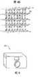
图1a是先有技术的像素阵列;Figure 1a is a prior art pixel array;
图1b是另一个先有技术的像素阵列;Figure 1b is another prior art pixel array;
图2a是本发明的一个像素阵列;Fig. 2a is a pixel array of the present invention;
图2b是本发明的一个备选实施例;Figure 2b is an alternative embodiment of the present invention;
图3是图表,以图形方式说明图2a和图2b的实现;Figure 3 is a diagram illustrating graphically the implementation of Figures 2a and 2b;
图4a是每行两个积分控制线的图示;Figure 4a is an illustration of two integral control lines per row;
图4b是每行一个积分时间信号线的图示;Figure 4b is an illustration of one integration time signal line per row;
图5是用于把图2a和图2b的像素阵列实现为优选商用实施例的照相机。Figure 5 is a camera for implementing the pixel array of Figures 2a and 2b into a preferred commercial embodiment.
具体实施方式Detailed ways
典型的先有技术图像传感器像素阵列如图1a和图1b所示。图1a中的图像传感器可能属于任何技术类型、如CCD或CMOS APS。图1a中的像素阵列10包括一组光电检测器。积分时间对于各像素是恒定的,由全部具有相同积分时间的区域10a中的像素代表。这种方法的缺点在于,如果积分时间长,则图像的亮区中的像素将变为饱和,以及亮区域中的图像细节将丢失。如果积分时间被选择为较短,则图像的暗区域中的图像质量因低信号和高噪声而会很差。在Guidash于2002年7月17日提交的标题为“具有可编程色彩平衡的有源像素传感器”的美国专利申请序号08/960418中公开了图1b中的图像传感器,在其中,与CFA图案关联的像素阵列20的各色彩具有各自的积分时间,以便取得电荷域白平衡。这在图1b中由表示为20a的区域即绿-红行中的绿像素、区域20b即绿-红行中的红像素、区域20c即绿-蓝行中的蓝像素以及区域20d即绿-蓝行中的绿像素来表示。这具有与对于图1a中的图像传感器像素阵列所述的相同缺点。Typical prior art image sensor pixel arrays are shown in Figures 1a and 1b. The image sensor in Figure 1a may be of any technology type such as CCD or CMOS APS. The pixel array 10 in Figure 1a includes a set of photodetectors. The integration time is constant for each pixel, represented by pixels in area 10a that all have the same integration time. The disadvantage of this method is that if the integration time is long, pixels in bright areas of the image will become saturated and image detail in bright areas will be lost. If the integration time is chosen to be short, the image quality in dark areas of the image will be poor due to low signal and high noise. The image sensor in Figure 1b is disclosed in U.S. Patent Application Serial No. 08/960418, filed July 17, 2002, entitled "Active Pixel Sensor with Programmable Color Balance," by Guidash, where the associated CFA pattern Each color of the pixel array 20 has its own integration time in order to achieve charge domain white balance. This is represented in FIG. 1b by the region 20a, the green pixels in the green-red row, the region 20b, the red pixels in the green-red row, the region 20c, the blue pixels in the green-blue row, and the region 20d, the green-red row. represented by green pixels in the blue row. This has the same disadvantages as described for the image sensor pixel array in Figure 1a.
参照图2a,本发明的图像传感器像素阵列30包括有助于不同的可编程积分时间、但按照与图1b所示不同的空间图案的阵列。对于x-y可寻址CMOS图像传感器,这可采用分开的传输门或复位门来实现。对于CCD图像传感器,这可通过包含分开的传输门来实现。图2a中的图像传感器像素阵列30构造成包括对于与滤色器阵列图案节距或核心相关的成对的行40a和40b具有两个不同积分时间的像素。具有长积分时间的像素称作快像素。具有短积分时间的像素称作慢像素。在Bayer CFA图案的情况中,这是两行节距。通过在这个图案中具有分开的积分时间,图像传感器的有效动态范围如图3所示被扩展。在区域1、即低亮度级区域中,传感器的慢和快两种像素没有饱和。快像素将具有远高于固有噪声电平的信号电平。慢像素将具有与传感器固有噪声电平相比在预定比率内的信号电平。在区域2中,慢和快两种像素都没有饱和,并且两者都具有足够的信噪比。在区域3、即高亮度级区域中,快像素已经饱和或者被削减,并且没有包含有效信号电平信息。慢像素没有饱和,并且包含具有足够信噪比的有效信号电平信息。由于有效信息与CFA图案相关,因此,来自快像素的丢失信息可通过慢像素的内插来确定。对于图3所示的分开积分时间体系结构,采取单帧捕捉,并且执行空间自适应图像处理。在区域2中,标准的先有技术彩色图像处理方法用来呈现图像。对于属于区域3中的图像捕捉中的像素面积,慢像素的内插用来确定快像素中的丢失信号信息。这导致图像的极亮面积中的真实MTF的损失,但是产生有效的更高饱和照度Isat。这有效地扩展图像传感器的画面内动态范围。虽然真实空间分辨率在极亮区域中下降,但是,在图像捕捉中原本会丢失的图像内容被保存。Referring to Figure 2a, the image
图2a的传感器体系结构设计成为积分时间图案提供第一积分时间的两行,以及具有第二积分时间的两个相邻行。这可采用任何类型的图像传感器、通过在这个图案中具有积分时间的多个或分开的控制来实现。对于CMOS和其它x-y可寻址图像传感器,这可只是通过让图像传感器定时采用应用于控制积分时间的交替行信号线对的独立的两组积分指针来安排来实现。这可能是各行中的传输门线或各行中的复位门线或者用来控制那一行的积分时间的其它任何每行信号。在CCD图像传感器的情况中,这要求构造传输门互连,使得至少对于行的交替对存在到传输门线的独立和分隔的连接。The sensor architecture of Figure 2a is designed to provide for an integration time pattern two rows with a first integration time, and two adjacent rows with a second integration time. This can be achieved with any type of image sensor by having multiple or split controls of integration times in this pattern. For CMOS and other x-y addressable image sensors, this can be achieved simply by having the image sensor timing arranged using two separate sets of integration pointers applied to alternating row pairs of signal lines that control the integration time. This could be a transfer gate line in each row or a reset gate line in each row or any other per-row signal used to control the integration time for that row. In the case of a CCD image sensor, this requires constructing the transmission gate interconnects such that at least for alternating pairs of rows there are independent and separate connections to the transmission gate lines.
本发明的第二实施例以图2b中的阵列来表示。在这个实施例中,传感器阵列50构造成在2×2像素图案60a和60b中具有两个分开且可编程的积分时间。在x-y可寻址图像传感器技术的情况中,这通过每行包括多个信号线来实现,它们用来控制积分时间,例如传输门或复位门。每行的多个信号线连接到像素的交替对,以便产生图2b所示的积分时间图案。A second embodiment of the invention is represented by the array in Figure 2b. In this embodiment,
参照图4a,说明控制积分时间的多个信号线70的路由选择。采用路由多个信号线70来控制各行的积分时间的一个缺点是填充因数减小或者更大的像素尺寸,以便使额外的信号线适合像素节距。这通过图4b所示的信号线路由选择体系结构来解决。在这种情况中,每行使用单个积分时间控制线80,但它实际上被路由到两个相邻行中的像素。相邻行中的信号线80以类似于创建图2b所示的积分时间图案的方式被路由。通过这种方法,虽然一次从传感器读出单行数据,但数据流中包含的像素是来自阵列中的物理上相邻的行。为了正确地重构图像,隔行数据必须在照相机图像存储器中进行校正。这也是本发明的一个特征。由于芯片上或照相机内的存储器可设置成把数据写入两行或两行以上的位置,因此不需要让传感器同时从物理行中读出所有像素。Referring to Figure 4a, the routing of a plurality of
如上所述,这为图像传感器和图像捕捉系统提供了画面内动态范围和宽曝光宽容度。单一图像捕捉可呈现具有对于低亮度级的积分时间的优化的全范围的图像信息,而没有削减图像的高亮度区域中的信号信息。这可极大地简化成像系统中的曝光控制系统和算法,因为曝光或积分时间的选择不需要非常精确。As mentioned above, this provides the image sensor and image capture system with in-frame dynamic range and wide exposure latitude. A single image capture can present a full range of image information with integration times optimized for low brightness levels without clipping signal information in high brightness regions of the image. This can greatly simplify exposure control systems and algorithms in imaging systems, since the choice of exposure or integration time does not need to be very precise.
还应当注意,采用这种传感器的图像捕捉系统可用来测量或确定画面的动态范围,以便适当设置两个积分时间。在照相机系统的计量阶段,两个分开很宽的积分时间可用来确定画面中的最大和最小亮度级。两个积分时间则可调整为覆盖画面中的照明范围。例如,如果要捕捉的画面的动态范围处于图像传感器的固有动态范围之内,则两个积分时间可设置为相同的值。如果画面包含比传感器的真实动态范围更宽的动态范围,则两个积分时间可设置为匹配或最佳地覆盖画面的动态范围。It should also be noted that an image capture system employing this sensor can be used to measure or determine the dynamic range of the frame in order to set the two integration times appropriately. In the metering stage of the camera system, two widely spaced integration times can be used to determine the maximum and minimum brightness levels in the frame. The two integration times can then be adjusted to cover the range of lighting in the frame. For example, if the dynamic range of the picture to be captured is within the intrinsic dynamic range of the image sensor, the two integration times can be set to the same value. If the picture contains a wider dynamic range than the sensor's true dynamic range, the two integration times can be set to match or optimally cover the dynamic range of the picture.
参照图5,说明用于实现本发明的图像传感器的照相机90,它是许多面向消费者的商业实施例之一。Referring to Figure 5, there is illustrated a
参照一个优选实施例描述了本发明。但是,大家会理解,本领域的技术人员可进行各种变更和修改,而没有背离本发明的范围。The invention has been described with reference to a preferred embodiment. However, it will be understood that various changes and modifications may be made by those skilled in the art without departing from the scope of the present invention.
配件表Accessories list
10 像素阵列10 pixel array
20 像素阵列20 pixel array
20a 绿像素,在绿-红行中20a green pixel, in green-red row
20b 红像素,在绿-红行中20b Red pixel, in green-red row
20c 蓝像素,在绿-蓝行中20c blue pixel, in green-blue row
20d 绿像素,在绿-蓝行中20d green pixels, in the green-blue row
30 像素阵列30 pixel array
40a 成对的行40a paired rows
40b 成对的行40b Paired lines
50 传感器阵列50 sensor array
60a 2×2像素图案60a 2×2 pixel pattern
60b 2×2像素图案60b 2×2 pixel pattern
70 多个信号线More than 70 signal lines
80 单积分时间控制线80 Single integral time control line
90 照相机90 cameras
Claims (3)
Translated fromChineseApplications Claiming Priority (3)
| Application Number | Priority Date | Filing Date | Title |
|---|---|---|---|
| US10/654,313 | 2003-09-03 | ||
| US10/654,313US7830435B2 (en) | 2003-09-03 | 2003-09-03 | Image sensor and image capture system with extended dynamic range |
| PCT/US2004/028325WO2005024948A2 (en) | 2003-09-03 | 2004-09-01 | Image sensor with extended dynamic range |
Related Child Applications (1)
| Application Number | Title | Priority Date | Filing Date |
|---|---|---|---|
| CN201110283424XADivisionCN102307282A (en) | 2003-09-03 | 2004-09-01 | Image sensor with extended dynamic range |
Publications (2)
| Publication Number | Publication Date |
|---|---|
| CN1843027A CN1843027A (en) | 2006-10-04 |
| CN1843027Btrue CN1843027B (en) | 2012-06-20 |
Family
ID=34218061
Family Applications (2)
| Application Number | Title | Priority Date | Filing Date |
|---|---|---|---|
| CN201110283424XAPendingCN102307282A (en) | 2003-09-03 | 2004-09-01 | Image sensor with extended dynamic range |
| CN200480024674XAExpired - LifetimeCN1843027B (en) | 2003-09-03 | 2004-09-01 | Image sensor with extended dynamic range |
Family Applications Before (1)
| Application Number | Title | Priority Date | Filing Date |
|---|---|---|---|
| CN201110283424XAPendingCN102307282A (en) | 2003-09-03 | 2004-09-01 | Image sensor with extended dynamic range |
Country Status (7)
| Country | Link |
|---|---|
| US (2) | US7830435B2 (en) |
| EP (1) | EP1661390A2 (en) |
| JP (1) | JP2007504770A (en) |
| KR (1) | KR101038386B1 (en) |
| CN (2) | CN102307282A (en) |
| TW (1) | TWI387334B (en) |
| WO (1) | WO2005024948A2 (en) |
Families Citing this family (46)
| Publication number | Priority date | Publication date | Assignee | Title |
|---|---|---|---|---|
| US7489352B2 (en)* | 2002-11-15 | 2009-02-10 | Micron Technology, Inc. | Wide dynamic range pinned photodiode active pixel sensor (APS) |
| FR2861242B1 (en)* | 2003-10-17 | 2006-01-20 | Trixell Sas | METHOD FOR CONTROLLING A PHOTOSENSITIVE DEVICE |
| US7446812B2 (en)* | 2004-01-13 | 2008-11-04 | Micron Technology, Inc. | Wide dynamic range operations for imaging |
| US8081234B2 (en)* | 2004-12-29 | 2011-12-20 | Intel Corporation | Technique for increased exposure range in image sensors |
| US7214998B2 (en)* | 2005-07-26 | 2007-05-08 | United Microelectronics Corp. | Complementary metal oxide semiconductor image sensor layout structure |
| KR100769548B1 (en) | 2005-12-30 | 2007-10-23 | 엠텍비젼 주식회사 | Color Filter Arrays and Image Interpolation Methods |
| JP4487944B2 (en)* | 2006-02-09 | 2010-06-23 | ソニー株式会社 | Solid-state imaging device |
| US20080198251A1 (en)* | 2007-02-15 | 2008-08-21 | Micron Technology, Inc. | Method, apparatus, and system providing multiple pixel integration periods |
| US20100044676A1 (en) | 2008-04-18 | 2010-02-25 | Invisage Technologies, Inc. | Photodetectors and Photovoltaics Based on Semiconductor Nanocrystals |
| EP2667412A1 (en) | 2007-04-18 | 2013-11-27 | Invisage Technologies, INC. | Materials, systems and methods for optoelectronic devices |
| KR101380615B1 (en)* | 2007-06-28 | 2014-04-14 | 삼성전자주식회사 | Method and apparatus for improving dynamic range of images |
| JP4480740B2 (en)* | 2007-07-03 | 2010-06-16 | シャープ株式会社 | Solid-state imaging device, manufacturing method thereof, and electronic information device |
| KR101424717B1 (en)* | 2007-09-13 | 2014-08-01 | 삼성전자주식회사 | Apparatus and method for setting exposure time |
| US8102435B2 (en) | 2007-09-18 | 2012-01-24 | Stmicroelectronics S.R.L. | Method for acquiring a digital image with a large dynamic range with a sensor of lesser dynamic range |
| US7940311B2 (en)* | 2007-10-03 | 2011-05-10 | Nokia Corporation | Multi-exposure pattern for enhancing dynamic range of images |
| US8203195B2 (en) | 2008-04-18 | 2012-06-19 | Invisage Technologies, Inc. | Materials, fabrication equipment, and methods for stable, sensitive photodetectors and image sensors made therefrom |
| US8405750B2 (en)* | 2009-06-08 | 2013-03-26 | Aptina Imaging Corporation | Image sensors and image reconstruction methods for capturing high dynamic range images |
| US8605177B2 (en)* | 2009-09-16 | 2013-12-10 | Altasens, Inc. | Image sensor with wide dynamic range |
| US8134628B2 (en)* | 2009-09-30 | 2012-03-13 | Truesense Imaging, Inc. | Methods for capturing and reading out images from an image sensor |
| US8279316B2 (en)* | 2009-09-30 | 2012-10-02 | Truesense Imaging, Inc. | Methods for capturing and reading out images from an image sensor |
| US8194166B2 (en) | 2009-09-30 | 2012-06-05 | Truesense Imaging, Inc. | Methods for capturing and reading out images from an image sensor |
| US20110074997A1 (en)* | 2009-09-30 | 2011-03-31 | Border John N | Methods for capturing and reading out images from an image sensor |
| US8279317B2 (en)* | 2009-09-30 | 2012-10-02 | Truesense Imaging, Inc. | Methods for capturing and reading out images from an image sensor |
| US8314873B2 (en) | 2009-09-30 | 2012-11-20 | Truesense Imaging, Inc. | Methods for capturing and reading out images from an image sensor |
| US8194165B2 (en) | 2009-09-30 | 2012-06-05 | Truesense Imaging, Inc. | Methods for capturing and reading out images from an image sensor |
| US8149303B2 (en)* | 2009-09-30 | 2012-04-03 | Truesense Imaging, Inc. | Methods for capturing and reading out images from an image sensor |
| US8194164B2 (en)* | 2009-09-30 | 2012-06-05 | Truesense Imaging, Inc. | Methods for capturing and reading out images from an image sensor |
| US8144220B2 (en) | 2009-09-30 | 2012-03-27 | Truesense Imaging, Inc. | Methods for capturing and reading out images from an image sensor |
| US8294803B2 (en)* | 2009-09-30 | 2012-10-23 | Truesense Imaging, Inc. | Methods for capturing and reading out images from an image sensor |
| WO2011156507A1 (en) | 2010-06-08 | 2011-12-15 | Edward Hartley Sargent | Stable, sensitive photodetectors and image sensors including circuits, processes, and materials for enhanced imaging performance |
| US8890986B2 (en)* | 2011-04-27 | 2014-11-18 | Aptina Imaging Corporation | Method and apparatus for capturing high dynamic range images using multi-frame interlaced exposure images |
| JP2012257193A (en) | 2011-05-13 | 2012-12-27 | Sony Corp | Image processing apparatus, image pickup apparatus, image processing method, and program |
| US8913153B2 (en) | 2011-10-06 | 2014-12-16 | Aptina Imaging Corporation | Imaging systems and methods for generating motion-compensated high-dynamic-range images |
| US8599284B2 (en)* | 2011-10-11 | 2013-12-03 | Omnivision Technologies, Inc. | High dynamic range sub-sampling architecture |
| US20130128083A1 (en)* | 2011-11-23 | 2013-05-23 | Himax Imaging Limited | High dynamic range image sensing device and image sensing method and manufacturing method thereof |
| US9172889B2 (en) | 2012-02-09 | 2015-10-27 | Semiconductor Components Industries, Llc | Imaging systems and methods for generating auto-exposed high-dynamic-range images |
| US9007488B2 (en) | 2012-03-08 | 2015-04-14 | Semiconductor Components Industries, Llc | Systems and methods for generating interpolated high-dynamic-range images |
| US9338372B2 (en) | 2012-09-19 | 2016-05-10 | Semiconductor Components Industries, Llc | Column-based high dynamic range imaging systems |
| JP2014086889A (en)* | 2012-10-24 | 2014-05-12 | Toshiba Corp | Solid-state imaging apparatus |
| CN103139491A (en)* | 2013-03-25 | 2013-06-05 | 天利半导体(深圳)有限公司 | A CMOS Sensor Chip with High Dynamic Range and Low Noise |
| US9941316B2 (en) | 2014-06-10 | 2018-04-10 | Invisage Technologies, Inc. | Multi-terminal optoelectronic devices for light detection |
| KR20160071203A (en) | 2014-12-11 | 2016-06-21 | 삼성전자주식회사 | Image signal processor, method for operating thereof, and mobile computing device including same |
| FR3050596B1 (en)* | 2016-04-26 | 2018-04-20 | New Imaging Technologies | TWO-SENSOR IMAGER SYSTEM |
| US11050945B2 (en) | 2018-07-06 | 2021-06-29 | Samsung Electronics Co., Ltd. | Method and apparatus for capturing dynamic images |
| CN110531401B (en)* | 2019-09-11 | 2021-04-09 | 南华大学 | Nuclear radiation detector and nuclear radiation detection method |
| KR20220101694A (en) | 2019-11-20 | 2022-07-19 | 기가조트 테크널러지 인코포레이티드 | Scalable pixel size image sensor |
Citations (1)
| Publication number | Priority date | Publication date | Assignee | Title |
|---|---|---|---|---|
| CN1205150A (en)* | 1996-09-27 | 1999-01-13 | 马库斯·伯姆 | locally adaptive optical sensor |
Family Cites Families (21)
| Publication number | Priority date | Publication date | Assignee | Title |
|---|---|---|---|---|
| US3971065A (en)* | 1975-03-05 | 1976-07-20 | Eastman Kodak Company | Color imaging array |
| EP0565295B1 (en)* | 1992-04-10 | 1997-11-26 | Mitsubishi Denki Kabushiki Kaisha | Rotating colour filter for a colour image display |
| JP3156503B2 (en)* | 1994-05-27 | 2001-04-16 | 松下電器産業株式会社 | Driving method of solid-state imaging device and signal processing circuit of solid-state imaging device |
| US6714239B2 (en)* | 1997-10-29 | 2004-03-30 | Eastman Kodak Company | Active pixel sensor with programmable color balance |
| US6999119B1 (en)* | 1998-04-10 | 2006-02-14 | Nikon Corporation | Image-capturing element, image-capturing circuit for processing signal from image-capturing element, image-capturing device, driving method of image-capturing element |
| US6831691B1 (en)* | 1998-04-15 | 2004-12-14 | Minolta Co., Ltd. | Solid-state image pickup device |
| US6665010B1 (en)* | 1998-07-21 | 2003-12-16 | Intel Corporation | Controlling integration times of pixel sensors |
| US7030917B2 (en)* | 1998-10-23 | 2006-04-18 | Hewlett-Packard Development Company, L.P. | Image demosaicing and enhancement system |
| US6069377A (en)* | 1999-05-13 | 2000-05-30 | Eastman Kodak Company | Image sensor incorporating saturation time measurement to increase dynamic range |
| US6307195B1 (en)* | 1999-10-26 | 2001-10-23 | Eastman Kodak Company | Variable collection of blooming charge to extend dynamic range |
| US6486504B1 (en)* | 1999-10-26 | 2002-11-26 | Eastman Kodak Company | CMOS image sensor with extended dynamic range |
| JP3707725B2 (en)* | 2000-05-30 | 2005-10-19 | 松下電器産業株式会社 | Still image solid-state imaging device |
| US6943837B1 (en)* | 1999-12-31 | 2005-09-13 | Intel Corporation | Method and apparatus for colormetric channel balancing for solid state image sensor using time division multiplexed sampling waveforms |
| JP2001352486A (en)* | 2000-06-07 | 2001-12-21 | Matsushita Electric Ind Co Ltd | Imaging device |
| JP2002185864A (en)* | 2000-12-12 | 2002-06-28 | Sony Corp | Solid-state imaging device and driving method thereof |
| WO2002056603A1 (en)* | 2001-01-09 | 2002-07-18 | Sony Corporation | Imaging device |
| US6943831B2 (en)* | 2001-01-24 | 2005-09-13 | Eastman Kodak Company | Method and apparatus to extend the effective dynamic range of an image sensing device and use residual images |
| JP3905708B2 (en)* | 2001-01-26 | 2007-04-18 | ペンタックス株式会社 | Image interpolation device |
| JP3627711B2 (en)* | 2002-02-14 | 2005-03-09 | ミノルタ株式会社 | Color imaging device |
| JP2003163937A (en)* | 2001-11-26 | 2003-06-06 | Fuji Photo Film Co Ltd | Solid-state imaging device and imaging apparatus |
| JP4097966B2 (en)* | 2002-03-22 | 2008-06-11 | オリンパス株式会社 | Image acquisition device |
- 2003
- 2003-09-03USUS10/654,313patent/US7830435B2/enactiveActive
- 2004
- 2004-09-01WOPCT/US2004/028325patent/WO2005024948A2/enactiveApplication Filing
- 2004-09-01CNCN201110283424XApatent/CN102307282A/enactivePending
- 2004-09-01EPEP04782749Apatent/EP1661390A2/ennot_activeWithdrawn
- 2004-09-01KRKR1020067004315Apatent/KR101038386B1/ennot_activeExpired - Lifetime
- 2004-09-01JPJP2006526154Apatent/JP2007504770A/enactivePending
- 2004-09-01CNCN200480024674XApatent/CN1843027B/ennot_activeExpired - Lifetime
- 2004-09-02TWTW093126565Apatent/TWI387334B/ennot_activeIP Right Cessation
- 2010
- 2010-10-06USUS12/898,809patent/US20110019040A1/ennot_activeAbandoned
Patent Citations (1)
| Publication number | Priority date | Publication date | Assignee | Title |
|---|---|---|---|---|
| CN1205150A (en)* | 1996-09-27 | 1999-01-13 | 马库斯·伯姆 | locally adaptive optical sensor |
Also Published As
| Publication number | Publication date |
|---|---|
| WO2005024948A2 (en) | 2005-03-17 |
| TWI387334B (en) | 2013-02-21 |
| CN1843027A (en) | 2006-10-04 |
| TW200520550A (en) | 2005-06-16 |
| EP1661390A2 (en) | 2006-05-31 |
| JP2007504770A (en) | 2007-03-01 |
| US7830435B2 (en) | 2010-11-09 |
| KR101038386B1 (en) | 2011-06-01 |
| CN102307282A (en) | 2012-01-04 |
| US20110019040A1 (en) | 2011-01-27 |
| US20050045980A1 (en) | 2005-03-03 |
| KR20060118425A (en) | 2006-11-23 |
| WO2005024948A3 (en) | 2005-09-01 |
Similar Documents
| Publication | Publication Date | Title |
|---|---|---|
| CN1843027B (en) | Image sensor with extended dynamic range | |
| US8350940B2 (en) | Image sensors and color filter arrays for charge summing and interlaced readout modes | |
| CN204633945U (en) | Image sensor, imaging system and processor system | |
| US7859581B2 (en) | Image sensor with charge binning and dual channel readout | |
| EP2339829B1 (en) | Sampling and readout of an image sensor | |
| KR100592619B1 (en) | Active pixel sensor with programmable color balance | |
| CN204720451U (en) | Imaging system and processor system | |
| CN205792895U (en) | Imaging system | |
| US20140332669A1 (en) | Arrangement of circuits in pixels, each circuit shared by a plurality of pixels, in image sensing apparatus | |
| CN108462841A (en) | Pel array and imaging sensor | |
| JPH1084507A (en) | Active pixel image sensor and method of manufacturing the same | |
| KR20110023802A (en) | Imaging Device and Camera System | |
| CN112770069B (en) | Image Installation | |
| CN109769095B (en) | Image sensor with multiple pixel access settings | |
| US8547458B2 (en) | Solid-state image pickup device | |
| CN207251823U (en) | Imaging device and imaging system | |
| JPH10189930A (en) | Solid-state imaging device | |
| Fossum | CMOS digital cameras need new figures of merit |
Legal Events
| Date | Code | Title | Description |
|---|---|---|---|
| C06 | Publication | ||
| PB01 | Publication | ||
| C10 | Entry into substantive examination | ||
| SE01 | Entry into force of request for substantive examination | ||
| ASS | Succession or assignment of patent right | Owner name:FULL VISION TECHNOLOGY CO., LTD. Free format text:FORMER OWNER: EASTMAN KODAK COMPANY (US) 343 STATE STREET, ROCHESTER, NEW YORK Effective date:20110706 | |
| C41 | Transfer of patent application or patent right or utility model | ||
| COR | Change of bibliographic data | Free format text:CORRECT: ADDRESS; FROM: NEW YORK STATE, THE USA TO: CALIFORNIA STATE, THE USA | |
| TA01 | Transfer of patent application right | Effective date of registration:20110706 Address after:California, USA Applicant after:Full Vision Technology Co.,Ltd. Address before:American New York Applicant before:Eastman Kodak Co. | |
| C14 | Grant of patent or utility model | ||
| GR01 | Patent grant | ||
| CP01 | Change in the name or title of a patent holder | ||
| CP01 | Change in the name or title of a patent holder | Address after:California, USA Patentee after:OmniVision Technologies, Inc. Address before:California, USA Patentee before:Full Vision Technology Co.,Ltd. | |
| CX01 | Expiry of patent term | ||
| CX01 | Expiry of patent term | Granted publication date:20120620 |