CN1841969B - Optical communication system, transmission deterioration compensation method, optical transmission system, and optical receiver system - Google Patents
Optical communication system, transmission deterioration compensation method, optical transmission system, and optical receiver systemDownload PDFInfo
- Publication number
- CN1841969B CN1841969BCN2005100931697ACN200510093169ACN1841969BCN 1841969 BCN1841969 BCN 1841969BCN 2005100931697 ACN2005100931697 ACN 2005100931697ACN 200510093169 ACN200510093169 ACN 200510093169ACN 1841969 BCN1841969 BCN 1841969B
- Authority
- CN
- China
- Prior art keywords
- optical
- polarization
- pulsed light
- station
- light
- Prior art date
- Legal status (The legal status is an assumption and is not a legal conclusion. Google has not performed a legal analysis and makes no representation as to the accuracy of the status listed.)
- Expired - Fee Related
Links
Images


Classifications
- H—ELECTRICITY
- H04—ELECTRIC COMMUNICATION TECHNIQUE
- H04B—TRANSMISSION
- H04B10/00—Transmission systems employing electromagnetic waves other than radio-waves, e.g. infrared, visible or ultraviolet light, or employing corpuscular radiation, e.g. quantum communication
- H04B10/50—Transmitters
- H04B10/501—Structural aspects
- H04B10/503—Laser transmitters
- H04B10/505—Laser transmitters using external modulation
- H—ELECTRICITY
- H04—ELECTRIC COMMUNICATION TECHNIQUE
- H04B—TRANSMISSION
- H04B10/00—Transmission systems employing electromagnetic waves other than radio-waves, e.g. infrared, visible or ultraviolet light, or employing corpuscular radiation, e.g. quantum communication
- H04B10/25—Arrangements specific to fibre transmission
- H04B10/2507—Arrangements specific to fibre transmission for the reduction or elimination of distortion or dispersion
- H04B10/2572—Arrangements specific to fibre transmission for the reduction or elimination of distortion or dispersion due to forms of polarisation-dependent distortion other than PMD
- H—ELECTRICITY
- H04—ELECTRIC COMMUNICATION TECHNIQUE
- H04B—TRANSMISSION
- H04B10/00—Transmission systems employing electromagnetic waves other than radio-waves, e.g. infrared, visible or ultraviolet light, or employing corpuscular radiation, e.g. quantum communication
- H04B10/50—Transmitters
- H04B10/501—Structural aspects
- H04B10/503—Laser transmitters
- H04B10/505—Laser transmitters using external modulation
- H04B10/5053—Laser transmitters using external modulation using a parallel, i.e. shunt, combination of modulators
- H—ELECTRICITY
- H04—ELECTRIC COMMUNICATION TECHNIQUE
- H04B—TRANSMISSION
- H04B10/00—Transmission systems employing electromagnetic waves other than radio-waves, e.g. infrared, visible or ultraviolet light, or employing corpuscular radiation, e.g. quantum communication
- H04B10/50—Transmitters
- H04B10/501—Structural aspects
- H04B10/503—Laser transmitters
- H04B10/505—Laser transmitters using external modulation
- H04B10/5059—Laser transmitters using external modulation using a feed-forward signal generated by analysing the optical or electrical input
- H04B10/50597—Laser transmitters using external modulation using a feed-forward signal generated by analysing the optical or electrical input to control the phase of the modulating signal
- H—ELECTRICITY
- H04—ELECTRIC COMMUNICATION TECHNIQUE
- H04B—TRANSMISSION
- H04B10/00—Transmission systems employing electromagnetic waves other than radio-waves, e.g. infrared, visible or ultraviolet light, or employing corpuscular radiation, e.g. quantum communication
- H04B10/50—Transmitters
- H04B10/58—Compensation for non-linear transmitter output
- H—ELECTRICITY
- H04—ELECTRIC COMMUNICATION TECHNIQUE
- H04B—TRANSMISSION
- H04B10/00—Transmission systems employing electromagnetic waves other than radio-waves, e.g. infrared, visible or ultraviolet light, or employing corpuscular radiation, e.g. quantum communication
- H04B10/60—Receivers
- H04B10/66—Non-coherent receivers, e.g. using direct detection
- H—ELECTRICITY
- H04—ELECTRIC COMMUNICATION TECHNIQUE
- H04J—MULTIPLEX COMMUNICATION
- H04J14/00—Optical multiplex systems
- H04J14/06—Polarisation multiplex systems
- H—ELECTRICITY
- H04—ELECTRIC COMMUNICATION TECHNIQUE
- H04B—TRANSMISSION
- H04B2210/00—Indexing scheme relating to optical transmission systems
- H04B2210/25—Distortion or dispersion compensation
- H04B2210/254—Distortion or dispersion compensation before the transmission line, i.e. pre-compensation
Landscapes
- Physics & Mathematics (AREA)
- Engineering & Computer Science (AREA)
- Computer Networks & Wireless Communication (AREA)
- Signal Processing (AREA)
- Electromagnetism (AREA)
- Optics & Photonics (AREA)
- Nonlinear Science (AREA)
- Optical Communication System (AREA)
Abstract
Translated fromChinese
Description
Translated fromChinese技术领域technical field
本发明总体上涉及光通信系统、传输劣化补偿方法、光传输系统以及光接收系统,更具体来说,涉及光信号的传输劣化得到补偿的光通信系统、传输劣化补偿方法、光传输系统以及光接收系统。The present invention generally relates to an optical communication system, a transmission degradation compensation method, an optical transmission system, and an optical receiving system, and more specifically, to an optical communication system in which transmission degradation of an optical signal is compensated, a transmission degradation compensation method, an optical transmission system, and an optical communication system. receiving system.
背景技术Background technique
例如,在光通信系统中,已使用了WDM(波分复用),其为用于将具有不同波长的多个数据信号复用到单条光纤中的方法。WDM(波分复用)通过利用具有不同波长的多个光束作为载波,使用光信号执行复用传输,其中,在光纤的发送侧设有光耦合器(复用器),在光纤的接收机侧设有光分路滤光器(去复用器)。For example, in an optical communication system, WDM (Wavelength Division Multiplexing), which is a method for multiplexing a plurality of data signals having different wavelengths into a single optical fiber, has been used. WDM (Wavelength Division Multiplexing) performs multiplexing transmission using optical signals by using multiple light beams with different wavelengths as carriers, in which an optical coupler (multiplexer) is provided There is an optical splitting filter (demultiplexer) on the side.
近来,在光通信系统中,其中针对各波长调制率为10Gbps的WDM已投入实际使用。为了进一步扩展传输容量,进而需要针对各波长调制率为40Gbps或80Gbps的WDM。Recently, in optical communication systems, WDM in which the modulation rate is 10 Gbps for each wavelength has been put into practical use. In order to further expand the transmission capacity, WDM with a modulation rate of 40Gbps or 80Gbps for each wavelength is required.
然而,在用于传输调制率超过40Gbps的光信号的光通信系统中,由偏振模色散(PMD)和偏振相关损耗(PDL)(几乎不会同时存在这些问题)导致的光信号波形失真的传输劣化将成为问题。However, in an optical communication system for transmitting an optical signal with a modulation rate exceeding 40Gbps, the transmission of the waveform distortion of the optical signal caused by polarization mode dispersion (PMD) and polarization dependent loss (PDL) (these problems hardly exist at the same time) Deterioration will be a problem.
偏振色散导致光信号波形失真。另一方面,通常,偏振模损耗几乎不成为问题。然而,当偏振模损耗累积时,光信号的偏振方向发生波动。因此,光信号电平会因从发光器件到受光元件的光路和偏振依赖性而发生波动。Polarization dispersion causes distortion of the optical signal waveform. On the other hand, in general, polarization mode loss is hardly a problem. However, when polarization mode losses accumulate, the polarization direction of the optical signal fluctuates. Therefore, the optical signal level fluctuates due to the optical path and polarization dependence from the light-emitting device to the light-receiving element.
在常规光通信系统中,使用了以下等方法:一种通过在接收机侧布置PMD/PDL补偿器来在接收部的前一级处对传输后的光信号的偏振色散进行补偿(例如,参见日本特开平第7-221705号公报),一种将传输本身更换为不会产生偏振色散的特殊光纤(例如,参见日本特开平第8-54525号公报)。In conventional optical communication systems, methods such as the following are used: One is to compensate the polarization dispersion of the transmitted optical signal at the previous stage of the receiving section by arranging a PMD/PDL compensator on the receiver side (for example, see Japanese Patent Laid-Open No. 7-221705), a special optical fiber in which the transmission itself is replaced with no polarization dispersion (see, for example, Japanese Patent Laid-Open No. 8-54525).
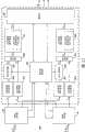
图1是示出一种使用单光纤传输单波长的光通信系统的系统配置示例的图。在图1的光通信系统中,终端站A和终端站B通过中继站A和中继站B相互连接。终端站A和终端站B中的每一个都包括用于发送光信号的光发送系统和用于接收光信号的光接收系统。FIG. 1 is a diagram showing an example of a system configuration of an optical communication system that transmits a single wavelength using a single optical fiber. In the optical communication system of FIG. 1, terminal station A and terminal station B are connected to each other through relay station A and relay station B. Each of the terminal station A and the terminal station B includes an optical transmission system for transmitting an optical signal and an optical reception system for receiving an optical signal.
终端站A和终端站B各自的光接收系统都包括用于补偿偏振色散的PMD补偿装置,和用于补偿偏振相关损耗的PDL补偿装置(例如,用于执行输出恒定控制的光学放大器)。然而,图1的光通信系统存在这样的问题,即,需要接收机侧始终测量偏振态的变化并对PMD补偿装置和PDL补偿装置进行复杂的控制。Each optical receiving system of terminal station A and terminal station B includes PMD compensating means for compensating for polarization dispersion, and PDL compensating means for compensating for polarization-dependent loss (for example, an optical amplifier for performing output constant control). However, the optical communication system of FIG. 1 has a problem that the receiver side is required to always measure the change of the polarization state and perform complicated control of the PMD compensating means and the PDL compensating means.
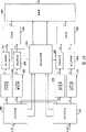
图2是示出一种使用单光纤传输双波长的光通信系统的系统配置示例的图。图3是示出一种双波长WDM复用器的配置示例的图。类似于图1的光通信系统,在图2的光通信系统中,终端站A和终端站B通过中继站A和中继站B相互连接。FIG. 2 is a diagram showing an example of a system configuration of an optical communication system that transmits two wavelengths using a single optical fiber. Fig. 3 is a diagram showing a configuration example of a two-wavelength WDM multiplexer. Similar to the optical communication system in FIG. 1 , in the optical communication system in FIG. 2 , terminal station A and terminal station B are connected to each other through relay station A and relay station B.
终端站A和终端站B中的每一个都具有图3所示的双波长WDM复用器。在该双波长WDM复用器中,在接收机侧针对各波长设有用于补偿偏振色散和偏振相关损耗的PMD/PDL补偿器。Each of the terminal station A and the terminal station B has a two-wavelength WDM multiplexer as shown in FIG. 3 . In the dual-wavelength WDM multiplexer, a PMD/PDL compensator for compensating polarization dispersion and polarization-dependent loss is provided for each wavelength on the receiver side.
然而,在图2的光通信系统中,要求在每个预定距离处针对各波长布置PMD/PDL补偿器。但是,与10Gbps的光通信系统相比,在对于单波长调制率为40Gbps或80Gbps的光通信系统中,系统成本昂贵。因此,难以在每个预定距离处针对各波长布置PMD/PDL补偿器。此外,存在传输信道用光纤的设置还很昂贵的问题。However, in the optical communication system of FIG. 2, it is required to arrange a PMD/PDL compensator for each wavelength at each predetermined distance. However, in an optical communication system with a modulation rate of 40 Gbps or 80 Gbps for a single wavelength, the system cost is expensive compared with an optical communication system of 10 Gbps. Therefore, it is difficult to arrange PMD/PDL compensators for each wavelength at each predetermined distance. In addition, there is a problem that installation of an optical fiber for a transmission channel is expensive.
此外,在偏振态快速变化的情况下,由于要求光通信系统跟上偏振态的变化并控制偏振相关损耗,不利的是,要求接收机侧针对各波长测量偏振态的变化并对PMD/PDL补偿器进行复杂的控制。In addition, in the case of rapid changes in the polarization state, since the optical communication system is required to keep up with the polarization state change and control the polarization-dependent loss, it is disadvantageous that the receiver side is required to measure the polarization state change for each wavelength and compensate for the PMD/PDL device for complex control.
发明内容Contents of the invention
本发明的总体目的是提供其中消除了上述问题的光通信系统、传输劣化补偿方法、光传输系统以及光接收系统。A general object of the present invention is to provide an optical communication system, a transmission degradation compensation method, an optical transmission system, and an optical receiving system in which the above-mentioned problems are eliminated.
本发明的一个更具体的目的是提供其中可以容易并廉价地补偿偏振色散和偏振相关损耗的光通信系统、传输劣化补偿方法、光传输系统以及光接收系统。A more specific object of the present invention is to provide an optical communication system, a transmission degradation compensation method, an optical transmission system, and an optical receiving system in which polarization dispersion and polarization-dependent loss can be easily and inexpensively compensated.
本发明的更具体的目的是提供一种光通信系统,其中,在发送机站处针对偏振色散和偏振相关损耗的影响进行预补偿,该影响是从发送机站向接收机站传输的光信号从通信信道接收到的;并且当接收机站接收到该光信号时来自传输信道的偏振色散和偏振相关损耗的影响被抵消。A more specific object of the present invention is to provide an optical communication system in which precompensation is performed at the transmitter station for the effects of polarization dispersion and polarization dependent loss on the optical signal transmitted from the transmitter station to the receiver station received from the communication channel; and the effects of polarization dispersion and polarization dependent loss from the transmission channel are canceled out when the receiver station receives the optical signal.
在优选模式下的本发明中,发送机站对偏振色散和偏振相关损耗进行预补偿,使得当在接收机站处接收光信号时偏振色散和偏振相关损耗的影响被抵消。从发送机站向接收机站传输的光信号通过传输信道传播,在该传输信道中产生了偏振色散和偏振相关损耗,并且该光信号受到该偏振色散和偏振相关损耗的影响。因此,在一个优选模式下的本发明中,在发送机侧对由传输信道引起的偏振色散和偏振相关损耗进行预补偿。因此,当从发送机站向接收机站传输光信号时光信号受到偏振色散和偏振相关损耗的影响,从而抵消了偏振色散和偏振相关损耗的影响。In the present invention in a preferred mode, the transmitter station precompensates for polarization dispersion and polarization dependent loss such that the effects of polarization dispersion and polarization dependent loss are canceled out when the optical signal is received at the receiver station. An optical signal transmitted from a transmitter station to a receiver station propagates through a transmission channel in which polarization dispersion and polarization-dependent loss are generated and affected by the polarization dispersion and polarization-dependent loss. Therefore, in a preferred mode of the invention, the polarization dispersion and polarization dependent losses caused by the transmission channel are precompensated at the transmitter side. Accordingly, the optical signal is affected by polarization dispersion and polarization dependent loss when transmitted from the sender station to the receiver station, thereby canceling out the effects of polarization dispersion and polarization dependent loss.
附图说明Description of drawings
当结合以下附图阅读时,根据以下详细描述,本发明的其他目的、特征和优点将变得更加清楚,附图中:Other objects, features and advantages of the present invention will become more apparent from the following detailed description when read in conjunction with the accompanying drawings, in which:
图1是示出一种使用单光纤传输单波长的光通信系统的系统配置示例的图;1 is a diagram showing an example of a system configuration of an optical communication system that transmits a single wavelength using a single optical fiber;
图2是示出一种使用单光纤传输双波长的光通信系统的系统配置示例的图;2 is a diagram showing an example of a system configuration of an optical communication system using a single optical fiber to transmit two wavelengths;
图3是示出一种双波长WDM复用器的配置示例的图;3 is a diagram showing a configuration example of a dual-wavelength WDM multiplexer;
图4是用于说明本发明的原理的图;Fig. 4 is a figure for explaining the principle of the present invention;
图5A、图5B、图5C以及图5D是示出用于说明本发明原理的波形的图;5A, FIG. 5B, FIG. 5C and FIG. 5D are diagrams showing waveforms used to illustrate the principles of the present invention;
图6是示出根据本发明第一实施例的光通信系统的系统配置的图;6 is a diagram showing a system configuration of an optical communication system according to a first embodiment of the present invention;
图7是示出根据本发明第一实施例的调制部的第一配置的图;7 is a diagram showing a first configuration of a modulation section according to a first embodiment of the present invention;
图8是示出根据本发明第一实施例的接收部中包括的第一配置部的图;8 is a diagram showing a first configuration section included in a reception section according to a first embodiment of the present invention;
图9是示出根据本发明第一实施例的接收部中包括的第二配置部的图;FIG. 9 is a diagram showing a second configuration section included in the receiving section according to the first embodiment of the present invention;
图10是示出根据本发明第一实施例的接收部中包括的第三配置部的图;FIG. 10 is a diagram showing a third configuration section included in the receiving section according to the first embodiment of the present invention;
图11是示出根据本发明第一实施例的调制部的第二配置的图;11 is a diagram showing a second configuration of a modulation section according to the first embodiment of the present invention;
图12是示出根据本发明第一实施例的调制部的第三配置的图;12 is a diagram showing a third configuration of a modulation section according to the first embodiment of the present invention;
图13是示出根据本发明第一实施例的接收机站中包括的接收部的第一配置的图;13 is a diagram showing a first configuration of a receiving section included in a receiver station according to a first embodiment of the present invention;
图14是示出根据本发明第一实施例的包括对端终端站的光通信系统的系统配置的第一变型的图;14 is a diagram showing a first modification of the system configuration of the optical communication system including the opposite terminal station according to the first embodiment of the present invention;
图15是示出根据本发明第一实施例的包括对端终端站的光通信系统的配置的第二变型的图;15 is a diagram showing a second modification of the configuration of the optical communication system including the opposite terminal station according to the first embodiment of the present invention;
图16A是示出根据本发明第一实施例的RZ码的一个时隙宽度的图,图16B是示出根据本发明第一实施例的偏振色散中出现的波劣化的图,图16C是示出根据本发明第一实施例的用于开/关调制器的最优定时以及分开波形的图,图16D是示出根据本发明第一实施例的用于开/关调制器的最优定时以及分开波形的图;16A is a diagram showing one slot width of the RZ code according to the first embodiment of the present invention, FIG. 16B is a diagram showing wave degradation occurring in polarization dispersion according to the first embodiment of the present invention, and FIG. 16C is a diagram showing Figure 16D shows the optimal timing for on/off modulators according to the first embodiment of the present invention and separate waveforms according to the first embodiment of the present invention. and a plot of the separated waveform;
图17是用于说明在使用同一波长的通信的情况下的临界系数(marginal factor)的图;FIG. 17 is a diagram for explaining a critical factor (marginal factor) in the case of communication using the same wavelength;
图18是用于说明根据本发明第一实施例的其中把回送10交替脉冲(backward 10 alternating pulse)的传输间隔设置得更长的传输示例的图;18 is a diagram for explaining a transmission example in which a transmission interval of backward 10 alternating pulses is set longer according to the first embodiment of the present invention;
图19是示出根据本发明第一实施例的接收机站中包括的接收部的第二配置的图;19 is a diagram showing a second configuration of a receiving section included in the receiver station according to the first embodiment of the present invention;
图20是示出根据本发明的调制部的第四配置的图;FIG. 20 is a diagram showing a fourth configuration of a modulation section according to the present invention;
图21是示出根据本发明第一实施例的调制部的第五配置的图;21 is a diagram showing a fifth configuration of a modulation section according to the first embodiment of the present invention;
图22是示出根据本发明第一实施例的调制部的第六配置的图;22 is a diagram showing a sixth configuration of a modulation section according to the first embodiment of the present invention;
图23是示出根据本发明第二实施例的调制部的第七配置的图;23 is a diagram showing a seventh configuration of a modulation section according to a second embodiment of the present invention;
图24是示出根据本发明第二实施例的使用两个波长的已接收回送10交替脉冲的图;Fig. 24 is a diagram showing received loopback 10 alternating pulses using two wavelengths according to a second embodiment of the invention;
图25是示出根据本发明第二实施例的能够抵消波长依赖性的发送机站的第一配置的图;25 is a diagram showing a first configuration of a transmitter station capable of canceling wavelength dependence according to a second embodiment of the present invention;
图26是示出根据本发明第二实施例的偏光分析器的第一配置的图;26 is a diagram showing a first configuration of a polarization analyzer according to a second embodiment of the present invention;
图27是示出根据本发明第二实施例的图25中的调制部的第一配置的图;FIG. 27 is a diagram showing a first configuration of a modulation section in FIG. 25 according to a second embodiment of the present invention;
图28是示出根据本发明第二实施例的图25中的调制部的第二配置的图;FIG. 28 is a diagram showing a second configuration of a modulation section in FIG. 25 according to a second embodiment of the present invention;
图29是示出根据本发明第二实施例的能够抵消波长依赖性的发送机站的第二配置的图;29 is a diagram showing a second configuration of a transmitter station capable of canceling wavelength dependence according to a second embodiment of the present invention;
图30是示出根据本发明第二实施例的能够抵消波长依赖性的发送机站的第三配置的图;30 is a diagram showing a third configuration of a transmitter station capable of canceling wavelength dependence according to a second embodiment of the present invention;
图31是示出根据本发明第二实施例的偏光分析器的第二配置的图;31 is a diagram showing a second configuration of a polarization analyzer according to a second embodiment of the present invention;
图32是示出根据本发明第二实施例的多波长源的第一配置的图;32 is a diagram showing a first configuration of a multi-wavelength source according to a second embodiment of the present invention;
图33是示出根据本发明第二实施例的多波长源的第二配置的图;33 is a diagram showing a second configuration of a multi-wavelength source according to a second embodiment of the present invention;
图34是示出根据本发明第二实施例的多波长源的第三配置的图;34 is a diagram showing a third configuration of a multi-wavelength source according to a second embodiment of the present invention;
图35是对其应用了本发明的终端站的第一配置的图;FIG. 35 is a diagram of a first configuration of a terminal station to which the present invention is applied;
图36是对其应用了本发明的终端站的第二配置的图;FIG. 36 is a diagram of a second configuration of a terminal station to which the present invention is applied;
图37是对其应用了本发明的中继站的第一配置的图;以及FIG. 37 is a diagram of a first configuration of a relay station to which the present invention is applied; and
图38是对其应用了本发明的中继站的第二配置的图。Fig. 38 is a diagram of a second configuration of a relay station to which the present invention is applied.
具体实施方式Detailed ways
以下参照附图对根据本发明的多个实施例进行描述。图4是用于说明本发明的原理的图。传输信道1是例如导致偏振色散和偏振相关损耗的波导。当假定光信号进入传输信道1的偏振方向是线偏振时,光信号的偏振角变得取决于偏振角而不同。Various embodiments according to the present invention will be described below with reference to the accompanying drawings. Fig. 4 is a diagram for explaining the principle of the present invention. The
然而,如果把其中传输率最小化的偏振角和其中传输率最大化的偏振角视为两个独立因素,那么当光信号沿传输信道1传播时,偏振面由于光信号的位移而相对于偏振轴旋转。However, if the polarization angle at which the transmission rate is minimized and the polarization angle at which the transmission rate is maximized are regarded as two independent factors, then when the optical signal propagates along the
此外,光纤的偏心率和其上长轴与短轴相互垂直的角面(anglesurface)并非在整个传输信道1中都是一致的,而是动态变化的。因此,由在传播过传输信道之后的偏振色散和偏振相关损耗所导致的传输劣化影响了进入传输信道1的光信号的偏振角。In addition, the eccentricity of the optical fiber and the angle surface on which the major axis and the minor axis are perpendicular to each other are not consistent throughout the
然而,如图4所示,当通过在传输信道1的接收机侧使偏振波旋转90度并反射该偏振波使其从传输终端折回时,抵消了由复杂的偏振色散的影响所导致的波形失真。作为其中使偏振波旋转90度的配置示例示出了光环行器(光学CIR)2和法拉第旋转器3。通过固定偏振的光纤把光环行器2与法拉第旋转器3相互连接起来。利用图4所示的原理,本发明通过抵消由于偏振失真和偏振相关损耗的影响而导致的复杂波形的失真,补偿了偏振色散和偏振相关损耗。However, as shown in FIG. 4, when the polarized wave is turned back from the transmission terminal by rotating the polarized wave by 90 degrees on the receiver side of the
图5A、图5B、图5C以及图5D是示出用于说明本发明原理的波形的图。在图5A到图5D中,x轴和y轴示出了其上x轴与y轴具有正交关系的偏振面。图5A示出了从接收机站向发送机站传输的光。图5B示出了在发送机站接收到的光。当在引起偏振色散和偏振相关损耗的传输信道中传播时,图5A所示的从接收机站向发送机站传输的光产生波形失真。图5B中的发送机站处接收到的光的偏振面由于偏振色散和偏振相关损耗的影响而旋转。5A, 5B, 5C, and 5D are diagrams showing waveforms for explaining the principle of the present invention. In FIGS. 5A to 5D , the x-axis and the y-axis show the plane of polarization on which the x-axis and the y-axis have an orthogonal relationship. Figure 5A shows light transmitted from a receiver station to a sender station. Figure 5B shows the light received at the transmitter station. The light transmitted from the receiver station to the transmitter station shown in FIG. 5A produces waveform distortion when propagating in the transmission channel causing polarization dispersion and polarization dependent loss. The plane of polarization of the light received at the transmitter station in Figure 5B is rotated due to the effects of polarization dispersion and polarization dependent loss.
在发送机站处,如图5C所示,对图5B所示的光进行调制的光信号的偏振波旋转90度。发送机站向接收机站传输光信号。图5D示出了在接收机站处接收到的光信号。At the transmitter station, as shown in FIG. 5C , the polarized wave of the optical signal modulating the light shown in FIG. 5B is rotated by 90 degrees. The transmitter station transmits an optical signal to the receiver station. Figure 5D shows the optical signal received at the receiver station.
图5C中的从发送机站向接收机站传输的光信号通过导致偏振色散和偏振相关损耗的传输信道传播。因此,与从接收机站向发送机站的传输类似,偏振面由于偏振色散和偏振相关损耗的影响而旋转。然而,由在图5C中从接收机站向发送机站传输光信号时导致的偏振色散和偏振相关损耗所影响的图5B中的光的偏振波旋转90度。The optical signal transmitted from the sender station to the receiver station in Fig. 5C propagates through the transmission channel causing polarization dispersion and polarization dependent loss. Thus, similar to the transmission from the receiver station to the transmitter station, the plane of polarization is rotated due to the effects of polarization dispersion and polarization dependent losses. However, the polarization of the light in FIG. 5B is rotated by 90 degrees, which is affected by polarization dispersion and polarization dependent loss caused when the optical signal is transmitted from the receiver station to the transmitter station in FIG. 5C.
结果,当图5C的光信号受到在从发送机站向接收机站传输光信号时导致的偏振色散和偏振相关损耗的影响时,偏振色散和偏振相关损耗的影响被抵消,光信号如图5D所示。在本发明中,由于当在接收机站处接收光信号时抵消了偏振色散和偏振相关损耗的影响,所以发送机站对偏振色散和偏振相关损耗进行了预补偿。在根据本发明的光通信系统中,可以在发送机站处针对各波长容易并合理地补偿偏振色散和偏振相关损耗。As a result, when the optical signal of Figure 5C is affected by the polarization dispersion and polarization-dependent loss caused when transmitting the optical signal from the sender station to the receiver station, the effects of polarization dispersion and polarization-dependent loss are canceled out, and the optical signal is shown in Figure 5D shown. In the present invention, the transmitter station precompensates for polarization dispersion and polarization dependent loss since the effects of polarization dispersion and polarization dependent loss are canceled out when the optical signal is received at the receiver station. In the optical communication system according to the present invention, polarization dispersion and polarization-dependent loss can be easily and reasonably compensated for each wavelength at the transmitter station.
以下,参照附图对本发明多个实施例进行描述。在这些实施例中,假定执行了对群速度色散的补偿。此外,在这些实施例中示出的WDM通信系统是利用WDM的光通信系统的一个示例。Hereinafter, various embodiments of the present invention will be described with reference to the accompanying drawings. In these embodiments, it is assumed that compensation for group velocity dispersion is performed. Also, the WDM communication system shown in these embodiments is an example of an optical communication system using WDM.
[第一实施例][first embodiment]
图6是示出根据本发明第一实施例的光通信系统的系统配置的图。在图6的光通信系统中,接收机站(终端站A)100通过传输信道300与发送机站(终端站B)200相互连接。若有必要,可以在传输信道300上布置一个或更多个中继站。FIG. 6 is a diagram showing a system configuration of an optical communication system according to a first embodiment of the present invention. In the optical communication system of FIG. 6 , a receiver station (terminal station A) 100 and a transmitter station (terminal station B) 200 are connected to each other through a
接收机站100包括LD光源101、LN调制器102、光学CIR或光学波长滤光器103以及接收部104。发送机站200包括光学CIR或光学波长滤光器201,以及调制部202。应当注意,光学CIR或光学波长滤光器201通过具有固定偏振波的多条光纤203与调制部202相互连接。The
在LN调制器102处把从接收机站100的接收部104的LD光源101输出的光调制成脉冲(回送10交替脉冲),并通过光学CIR或用于对接收光和发送光进行去复用的光学波长滤光器103向传输信道300输出该脉冲。发送机站200的调制部202通过光学CIR或用于对接收光和发送光进行去复用的光学波长滤光器201接收脉冲(接收到的回送10交替脉冲),并将该脉冲调制成光信号。调制部202通过光学CIR或光学波长滤光器201输出被调制到传输信道300的光信号。The light output from the LD
接收机站100的接收部104通过光学CIR或光学波长滤光器103接收该光信号。根据上述本发明的原理,在接收部104处接收到的光信号具有其中抵消了传输信道300的偏振色散和偏振相关损耗的影响的波形。The receiving
然而,如果发送机站200无法检测出从接收机站100接收的由于偏振色散和偏振相关损耗而失真的波形的哪一位表示脉冲,则发送机站200无法将该脉冲调制成调制信号(待传输信号)。However, if the
图7是示出根据本发明第一实施例的调制部的第一配置的图。调制部202a包括偏光去复用器210、分路装置211和212、调制器213和214、偏光正交复用器215、90度偏光旋转器216、受光元件217和218、滤波器219和220、以及调制定时相位调节电路221。FIG. 7 is a diagram showing a first configuration of a modulation section according to the first embodiment of the present invention. The
偏光去复用器210是用于对要分离的两个偏光进行去复用的装置,偏光正交复用器215是用于使两个偏光相交并对其进行复用的装置。偏光去复用器210和偏光正交复用器215中的每一个都由布儒斯特效应器件组成。分路装置211和212是用于使光分路的装置,并由光耦合器(光CPL)等组成。在分路装置211和212处,响应于光电可以选择性地设置比率,如1∶10。每个调制器213和214都由马赫-曾德尔型LINO3调制器、电吸收调制器等组成。每个受光元件217和218都由光电二极管等组成。The
例如,当接收机站100(图6)针对各波长把光调制成回送10交替脉冲并向发送机站200(图6)传输正在调制的光时,偏光去复用器210接收来自接收机站100并由光学CIR或光学波长滤光器201(图6)解调后的已接收回送10交替脉冲。偏光去复用器210把正在接收的已接收回送10交替脉冲去复用成两个偏光。偏光去复用器210通过相应的分路装置211和212向调制器213和214传输所接收并经去复用的已接收回送10交替脉冲。分路装置211和212使该回送10交替脉冲分路,然后向受光元件217和218传输该回送10交替脉冲。For example, when the receiver station 100 (FIG. 6) modulates light to return 10 alternating pulses for each wavelength and transmits the light being modulated to the transmitter station 200 (FIG. 6), the
受光元件217和218对已接收回送10交替脉冲的电气电平进行转换,并向相应的滤波器219和220传输该电气电平。每个滤波器219和220都分别从自受光元件217和218接收到的电气电平提取时钟,然后向调制定时相位调节电路221传输该时钟。调制定时相位调节电路221按基于从相应的滤波器219和220接收到的时钟的定时向调制器213和214传输调制信号。The
调制器213和214利用从调制定时相位调节电路221接收的调制信号对从偏光去复用器210通过相应的分路装置211和212接收到的已接收回送10交替脉冲进行调制,并作为光信号向偏光正交复用器215传输该已接收回送10交替脉冲。偏光正交复用器215使接收到的光信号相交并将其复用成复用光信号,并向90度偏光旋转器216传输该复用光信号。90度偏光旋转器216使该复用光信号的偏振波旋转90度。通过光学CIR或光学波长滤光器201向传输信道300输出其偏振波旋转90度的复用光信号,作为光信号。The
接收机站100中包括的光传输系统由偏光固定光电路组成。在该光传输系统中,不存在偏振波的旋转。将该光传输系统设计成保持接收到的偏振态。如图8、图9或图10所示,通过在LN调制器102与光学CIR或光学波长滤光器103之间额外地设置配置部110a,使从接收机站100传输的回送10交替脉冲保持偏振态稳定。The optical transmission system included in the
图8是示出根据本发明第一实施例的接收部中包括的第一配置部的图。图8的第一配置部110a包括偏光去复用器110、光学强度调节装置111和112以及偏光正交复用器113。每个光学强度调节装置111和112都是用于调节光电平的装置,例如由不具有偏振依赖性的电吸收光衰减器等组成。Fig. 8 is a diagram showing a first configuration section included in a receiving section according to a first embodiment of the present invention. The first configuration section 110 a of FIG. 8 includes a polarization demultiplexer 110 , optical intensity adjustment devices 111 and 112 , and a polarization quadrature multiplexer 113 . Each of the optical intensity adjustment devices 111 and 112 is a device for adjusting the light level, for example, consists of an electro-absorption optical attenuator that has no polarization dependence or the like.
偏光去复用器110把回送10交替脉冲去复用成两个偏光。偏光去复用器110向光学强度调节装置111和112传输去复用成两个偏光的回送10交替脉冲。光学强度调节装置111和112调节回送10交替脉冲的光电平,并向偏光正交复用器113传输该回送10交替脉冲。在偏光正交复用器113使正接收的回送10交替脉冲相交并对其进行复用之后,偏光正交复用器113向传输信道300输出该回送10交替脉冲。A polarization demultiplexer 110 demultiplexes the loopback 10 alternating pulses into two polarizations. The polarization demultiplexer 110 transmits the loopback 10 alternate pulses demultiplexed into two polarizations to the optical intensity adjustment devices 111 and 112 . The optical intensity adjustment devices 111 and 112 adjust the optical level of the loopback 10 alternate pulses, and transmit the loopback 10 alternate pulses to the polarization quadrature multiplexer 113 . After the polarizing quadrature multiplexer 113 intersects and multiplexes the loopback 10 alternate pulses being received, the polarizer quadrature multiplexer 113 outputs the loopback 10 alternate pulses to the
图9是示出根据本发明第一实施例的接收机站中包括的第二配置部的图。除了第二配置部110b的一个部分以外,图9的第二配置部110b具有与图8的第一配置部110a相似的配置,以下适当略去对其的阐述。图9的第二配置部110b包括偏光去复用器110、光学强度调节装置111和112、偏光正交复用器113以及偏光独立调制器114。FIG. 9 is a diagram showing a second configuration section included in the receiver station according to the first embodiment of the present invention. Except for a part of the second configuration part 110b, the second configuration part 110b of FIG. 9 has a configuration similar to that of the first configuration part 110a of FIG. 8, and the explanation thereof will be appropriately omitted below. The second configuration section 110 b of FIG. 9 includes a polarization demultiplexer 110 , optical intensity adjustment devices 111 and 112 , a polarization quadrature multiplexer 113 , and a polarization independent modulator 114 .
例如,偏光去复用器110接收从LD光源101输出的光,并把该光去复用成两个偏光。偏光去复用器110向光学强度调节装置111和112传输正被去复用的光。光学强度调节装置111和112调节正在接收的光的光电平,并向偏光正交复用器113传输该光。在偏光正交复用器113使接收到的光相交并对其进行复用之后,偏光正交复用器113向传输信道300(图6)输出该接收到的光。For example, the polarization demultiplexer 110 receives the light output from the LD
图10是示出根据本发明第一实施例的接收机站中包括的第三配置部的图。图10的第三配置部110c具有利用了单向偏振面的配置。图10的第三配置部110c包括偏光器115、光学强度调节装置116等。Fig. 10 is a diagram showing a third configuration section included in the receiver station according to the first embodiment of the present invention. The
在偏光器115把接收到的回送10交替脉冲改变成单偏光之后,偏光器115向光学强度调节装置116输出该单偏光。在光学强度调节装置116调节了回送10交替脉冲的光电平之后,光学强度调节装置116向传输信道300(图6)输出该回送10交替脉冲。例如,对于在向接收部104的受光元件的任何光路上布置有具有更高偏振相关损耗的装置的情况,通过第三配置部110c可以获得更好的效果。After the
通过如图8、图9或图10所示附加设置接收机站100的配置部110a、110b或100c,发送机站200可以应对由传输信道300导致的偏振色散和偏振相关损耗。此外,发送机站200的调制部202可以具有如图11或图12所示的配置。By additionally disposing configuration section 110a, 110b or 100c of
图11是示出根据本发明第一实施例的调制部的第二配置的图。图11中,除了调制部202b的两个部分以外,调制部202b具有与图7的调制部202a相似的配置,以下适当略去对其的阐述。图11的调制部202b包括偏光去复用器210、分路装置211和212、调制器213和214、偏光正交复用器215、90度偏光旋转器216、受光元件217和218、滤波器219和220、调制定时相位调节电路221、偏光旋转器222以及相位差检测器223。FIG. 11 is a diagram showing a second configuration of a modulation section according to the first embodiment of the present invention. In FIG. 11 , the
偏光旋转器222是用于使光的偏振面旋转的装置。例如,通过向石榴石晶体(garnet crystal)等施加磁场,偏振面由于法拉第效应而旋转。例如,当接收机站100针对把各波长的光调制成回送10交替脉冲并向发送机站200传输该回送10交替脉冲时,偏光旋转器222接收从接收机站100发送并由光学CIR或光学波长滤光器201去复用后的已接收回送10交替脉冲。The
偏光旋转器222使该已接收回送10交替脉冲的偏振面旋转,使得该要由偏光去复用器210去复用的已接收回送10交替脉冲的延迟差变得最大。相位差检测器223控制由偏光旋转器222对已接收回送10交替脉冲的偏振面进行的旋转。偏光去复用器210接收该已接收回送10交替脉冲,其中旋转了偏振面。偏光去复用器210通过相应的分路装置211和212向调制器213和214传输正被去复用成两个偏光的已接收回送10交替脉冲。分路装置211和212使从偏光去复用器210接收到的已接收回送10交替脉冲分路,然后向受光元件217和218传输该已接收回送10交替脉冲。The
受光元件217和218把从相应的分路装置211和212接收到的已接收回送10交替脉冲的光电平转换成电气电平,然后向相应的滤波器219和220传输该电气电平。每个滤波器219和220都从该电气电平提获取时钟,并向相位差检测器223传输该时钟。相位差检测器223把从滤波器219和220接收到的时钟传输给调制定时相位调节电路221。The
此外,相位差检测器223响应于来自滤波器219和220的时钟检测由偏光去复用器210对其进行去复用的已接收回送10交替脉冲的相位差。相位差检测器223对偏光旋转器222进行控制,使得由偏光去复用器210对其进行去复用的已接收回送10交替脉冲的延迟差变得最大。此外,调制定时相位调节电路221按基于从相应的滤波器219和220接收的时钟的定时向调制器213和214传输调制信号。Further, the
每个调制器213和214都利用从调制定时相位调节电路221接收的调制信号对从偏光去复用器210通过相应的分路装置211和212接收到的已接收回送10交替脉冲进行调制,并向偏光正交复用器215传输该正被调制的已接收回送10交替脉冲。偏光正交复用器215使接收到的光信号相交并将其复用成复用光信号,并向90度偏光旋转器216传输该复用光信号。90度偏光旋转器216使该复用光信号的偏振波相对于由偏光旋转器222对偏振面进行的旋转相对旋转90度。由90度偏光旋转器216旋转90度后的偏振波通过光学CIR或光学波长滤光器201输出至传输信道300。Each
在图11的调制部202b中,偏光旋转器222使己接收回送10交替脉冲的偏振面旋转,使得该由偏光去复用器210去复用的已接收回送10交替脉冲的延迟差变得最大。根据调制部202b的该配置,可以清楚地分离其膨胀由于偏振色散而变得最大的波形。由此,可以改进性能。在图11的调制部202b中,在由偏光旋转器222旋转了偏振波之后,不必由90度偏光旋转器216相对地旋转偏振面。In the modulator 202b of FIG. 11 , the
图12是示出根据本发明第一实施例的调制部的第三配置的图。图12中,除了调制部202c的某些部分以外,调制部202c具有与图7的调制部202a或图11的调制部202b相似的配置,以下适当略去对其的阐述。图12的调制部202c包括偏光去复用器210、分路装置211和212、调制器213和214、偏光正交复用器215、90度偏光旋转器216、受光元件217和218、滤波器219和220、调制定时相位调节电路221、光学强度调节装置224和225、分路装置226和227、受光元件228和229以及功率电平率检测率调节控制电路230。FIG. 12 is a diagram showing a third configuration of a modulation section according to the first embodiment of the present invention. In FIG. 12 , except for some parts of the modulation unit 202c, the modulation unit 202c has a configuration similar to that of the
偏光去复用器210把正被接收的已接收回送10交替脉冲去复用成两个偏光,并通过分路装置211和212向调制器213和214输出已接收回送10交替脉冲。分路装置211和212使该已接收回送10交替脉冲分路并将其传输给受光元件217和218。The
受光元件217和218把接收的回送10交替脉冲的光电平转换成电气电平,然后把该电气电平传输给相应的滤波器219和220。每个滤波器219和220都从自相应的受光元件217和218接收到的该电气电平提取时钟,并把该时钟传输给调制定时相位调节电路221。The
此外,每个受光元件217和218都向功率电平率检测率调节控制电路230传输从已接收回送10交替脉冲的光电平转换成的电气电平。调制定时相位调节电路221按基于从受光元件217和218接收的时钟的定时向调制器213和214传输调制信号。In addition, each of the
调制器213和214通过该调制信号对(从相应的分路装置211和212接收的已接收回送10交替脉冲进行调制,并把该已接收回送10交替脉冲作为光信号传输给相应的光学强度调节装置224和225。在光学强度调节装置224和225调节了从相应的调制器213和214接收的光信号的电平之后,光学强度调节装置224和225通过分路装置226和227向偏光正交复用器215传输该光信号的电平。应当注意,由功率电平率检测率调节控制电路230控制由各光学强度调节装置224和225对光信号的电平执行的每个调节。The
分路装置226和227使从相对光学强度调节装置224和225接收的光信号分路到相应的受光元件228和229。受光元件228和229把该光信号的电平转换成电气电平,并将该电气电平传输给功率电平率检测率调节控制电路230。The branching devices 226 and 227 branch the optical signals received from the relative optical intensity adjusting devices 224 and 225 to corresponding light receiving elements 228 and 229 . The light receiving elements 228 and 229 convert the level of the optical signal into an electrical level, and transmit the electrical level to the power level rate detection rate adjustment control circuit 230 .
功率电平率检测率调节控制电路230响应于从各受光元件228和229接收的电平控制由各光学强度调节装置224和225对光信号电平执行的调节。The power level rate detection rate adjustment control circuit 230 controls the adjustment of the optical signal level performed by the respective optical intensity adjustment devices 224 and 225 in response to the level received from the respective light receiving elements 228 and 229 .
偏光正交复用器215使从分路装置226和227接收的光信号相交并将其复用成复用光信号,并把该复用光信号传输给90度偏光旋转器216。90度偏光旋转器216使该复用光信号的偏振波旋转90度。通过光学CIR或光学波长滤光器201把其偏振波由90度偏光旋转器216旋转了90度的复用光信号作为光信号输出给传输信道300。在图12的调制部202中,由于可以调节光信号电平,所以可以补偿偏振相关损耗。通常,可以控制偏振相关损耗,使得光电平在接收机站侧恒定。然而,这需要针对每个波长控制偏振相关损耗。在该WDM通信系统中,例如,即使光学放大器进行控制使得总功率电平输出恒定,也不存在影响。The
如上所述,发送机站200的调制部202把已接收回送10交替脉冲的光波形转换成电信号,并向滤波器219和220传输该电信号。每个滤波器219和220都从自调制部202接收的电信号提取时钟,并把该时钟传输给调制定时相位调节电路221。As described above, the modulating
在调制定时相位调节电路221按基于从滤波器219和220接收的时钟的定时调节了调制信号的相位之后,调制定时相位调节电路221把该调制信号传输给调制器213和214。调制器213和214通过使从已接收回送10交替脉冲提取的时钟同步化,对从相应的分路装置211和212接收到的已接收回送10交替脉冲进行调制。After the modulation timing
如果不使从已接收回送10交替脉冲提取的时钟同步化就进行调制,那么在接收机站100处脉冲宽度会减小。通过如图13所示地配置接收机站100的接收部104,可以监测脉冲宽度并向调制部202传输相位调节用信息。If the modulation is performed without synchronizing the clock drawn from the alternate pulses of the received loopback 10, the pulse width at the
图13是示出根据本发明第一实施例的接收机站中包括的接收部的第一配置的图。图13的接收部104-1包括受光元件121、解调电路122、脉冲宽度检测电路123、时钟定时提取部124以及监测器控制信号发送部125。Fig. 13 is a diagram showing a first configuration of a receiving section included in a receiver station according to the first embodiment of the present invention. The reception unit 104 - 1 in FIG. 13 includes a
受光元件121通过光学CIR或光学波长滤光器103从发送机站200接收光信号。受光元件121把该光信号的光电平转换成电气电平,并将该电气电平传输给脉冲宽度检测电路123和时钟定时提取部124。The
时钟定时提取部124从自受光元件121接收的电气电平提取时钟。解调电路122对从受光元件121接收的电气电平进行解调,并作为解调信号(接收数据)输出正被解调的电气电平。脉冲宽度检测电路123根据从受光元件121接收的电气电平和从解调电路122接收的解调信号,检测脉冲宽度。脉冲宽度检测电路123把检测到的脉冲宽度通知给监测器控制信号发送部125。The clock
监测器控制信号发送部125根据脉冲宽度检测电路123通知的脉冲宽度,向发送机站200的调制部202传输相位调节用信息。例如,该相位调节用信息包括在与主信号波长的波长差进行复用的SV信号中,或者包括在主信号附加(OH)信息(overhead information)中,并把该相位调节用信息传输给发送机站200的调制部202。The monitor control signal transmission unit 125 transmits phase adjustment information to the
然而,发送机站200的调制部202可以通过使从己接收回送10交替脉冲提取的时钟同步化,对各波长进行调制。结果,发送机站200的调制部202可以调节相位,使得在接收机站100的接收部104-1处脉冲宽度变得最大(在RZ(归零)码的情况下占空比为50%)。However, the
图14是示出包括根据本发明第一实施例的对端终端站的光通信系统的系统配置的第一变型的图。在图14的光通信系统中,终端站100a与终端站200a通过传输信道300a和300b相互连接。应当注意,若有必要,可以在传输信道300a和300b上布置一个或更多个中继站。14 is a diagram showing a first modification of the system configuration of the optical communication system including the counterpart terminal station according to the first embodiment of the present invention. In the optical communication system of FIG. 14, a
每个终端站100a和200a都包括用于传输光信号的光传输系统,和用于接收光信号的光接收系统。终端站100a包括:光接收系统,其包括光学CIR或光学波长滤光器103a;发送部130a;帧/OH处理部131a;光传输系统,其包括光学CIR或光学波长滤光器201b;调制部202b;以及帧/OH处理部240b。Each of the
终端站200a包括:光接收系统,其包括接收部104b、光学CIR或光学波长滤光器103a;发送部130b;帧/OH处理部131b;光传输系统,其包括光学CIR或光学波长滤光器201a;调制部202a;以及帧/OH处理部240a。The
如上参照图8到图10所述地配置发送部130a和130b。如上参照图13所述地配置接收部104a和104b。此外,如上参照图7、图11以及图12所述地配置调制部202a和202b。应当注意,图14的光通信系统的第三配置类似于上述配置,以下适当略去对其的阐述。The transmitting
在图14的光通信系统中,如下所述地从光接收系统向光传输系统传输相位调节用信息。接收部104a把相位调节用信息传输给帧/OH处理部240b。帧/OH处理部240把相位调节用信息包括在附加信息中。In the optical communication system of FIG. 14, information for phase adjustment is transmitted from the optical receiving system to the optical transmission system as follows. The receiving
在向终端站200a传输了相位调节用信息之后,由帧/OH处理部131b从附加信息获取包括在该附加信息中的相位调节用信息,并将其传输给调制部202a的调制定时相位调节电路221a。因此,调制部202a通过利用从帧/OH处理部131b接收的相位调节用信息调节相位,使得在终端站100a的接收部104a处脉冲宽度变得最大。After the information for phase adjustment is transmitted to the
接收部104b向帧/OH处理部240a传输相位调节用信息。帧/OH处理部240a把从接收部104b接收的相位调节用信息包括在附加信息中。The receiving
在向终端站100a传输了包括在附加信息中的相位调节用信息之后,在帧/OH处理部131a处从附加信息获取相位调节用信息,并将其传输给调制部202b的调制定时相位调节电路221b。因此,调制部202b可以通过利用从帧/OH处理部131a接收的相位调节用信息调节相位,使得在终端站200a的接收部104b处脉冲宽度变得最大。After the phase adjustment information included in the additional information is transmitted to the
此外,图15是示出包括根据本发明第一实施例的对端终端站的光通信系统配置的第二变型的图。除了图14的配置的某些部分以外,光通信系统配置的第二变型类似于图14的配置,以下适当略去对其的阐述。应当注意,图15的光通信系统配置中略去并且未示出帧/OH处理部。Furthermore, FIG. 15 is a diagram showing a second modification of the configuration of the optical communication system including the counterpart terminal station according to the first embodiment of the present invention. The second modification of the configuration of the optical communication system is similar to the configuration of FIG. 14 except for some parts of the configuration of FIG. 14 , and explanation thereof is appropriately omitted below. It should be noted that the frame/OH processing section is omitted and not shown in the optical communication system configuration of FIG. 15 .
与图14的终端站100a不同,图15的终端站100b包括波长滤光器132a和241b,以及监测器波长CH发送机/接收机133。波长滤光器132a布置在光学CIR或光学波长滤光器103a与接收部104a之间。波长滤光器241b布置在光学CIR或光学波长滤光器201b与调制部202b之间。此外,监测器波长CH发送机/接收机133布置在波长滤光器132a与接收部104a之间,以及波长滤光器241b与调制部202b之间。Unlike the
与图14的终端站200a不同,终端站200b包括波长滤光器132b和241a,以及监测器波长CH发送机/接收机134。波长滤光器132b布置在光学CIR或光学波长滤光器103b与接收部104a之间。波长滤光器241a布置在光学CIR或光学波长滤光器201a与调制部202a之间。此外,监测器波长CH发送机/接收机134布置在波长滤光器132b与接收部104b之间,以及波长滤光器241a与调制部202a之间。Unlike the
在图15的光通信系统中,如下所述地从光接收系统向光传输系统传输相位调节用信息。接收部104a把相位调节用信息传输给监测器波长CH发送机/接收机133。监测器波长CH发送机/接收机133通过波长滤光器241b把相位调节用信息复用到光信号中。In the optical communication system of FIG. 15, information for phase adjustment is transmitted from the optical receiving system to the optical transmission system as follows. The
在向终端站200b传输了被复用到光信号中的相位调节用信息之后,由波长滤光器132b从光信号获取该信息,并通过调制波长CH发送机/接收机134将该信息传输给调制部202a的调制定时相位调节电路221a。因此,调制部202a可以通过利用该相位调节用信息来调节相位,使得在终端站100b的接收部104a处脉冲宽度变得最大。After transmitting the information for phase adjustment multiplexed into the optical signal to the
接收部104b向监测器波长CH发送机/接收机134传输相位调节用信息。监测器波长CH发送机/接收机134通过波长滤光器241a把该相位调节用信息复用到光信号中。The receiving
在向终端站100b传输了被复用到光信号中的相位调节用信息之后,由波长滤光器132a获取该信息,并通过监测器波长CH发送机/接收机133将该信息传输给调制部202b的调制定时相位调节电路221b。因此,调制部202b可以通过利用该相位调节用信息调节相位,使得在终端站200b的接收部104b处脉冲宽度变得最大。After the information for phase adjustment multiplexed into the optical signal is transmitted to the
在图16A到图16D中将示出其中在接收部处脉冲宽度变得最大的相位。图16A是示出根据本发明第一实施例的RZ码的一个时隙宽度的图。图16B是示出根据本发明第一实施例的偏振色散中的波劣化表现的图。图16C和图16D是示出根据本发明第一实施例的用于开/关调制器的最优定时以及分开波形的图。例如,在根据本发明的光通信系统中,通过控制图16C和图16D所示的调制器213和214的开/关,可以明显地分开图16B所示的波形。The phase in which the pulse width becomes maximum at the receiving section will be shown in FIGS. 16A to 16D . FIG. 16A is a diagram showing one slot width of the RZ code according to the first embodiment of the present invention. FIG. 16B is a graph showing the behavior of wave degradation in polarization dispersion according to the first embodiment of the present invention. 16C and 16D are graphs showing optimal timing and split waveforms for an on/off modulator according to the first embodiment of the present invention. For example, in the optical communication system according to the present invention, by controlling on/off of the
在图6的系统配置中,在接收机站100中的发送方向上的光与接收方向上的光具有相同的波形。因此,如图17所示,在光学CIR或光学波长滤光器103处无法充分地分开发送方向与接收方向上的光单元。不利的是,传输距离变长了,或者由于传输信道300的反射而无法进行通信。In the system configuration of FIG. 6, the light in the transmission direction and the light in the reception direction in the
图17是用于说明在使用同一波长的通信的情况下的临界系数的图。当在接收机站100附近的传输信道300处发生反射时,接收光与反射折回光相互重叠。应当注意,传输距离越长,在接收部104处接收到的光信号的接收电平就越小。结果,接收部104无法识别数据。FIG. 17 is a diagram for explaining critical coefficients in the case of communication using the same wavelength. When a reflection occurs at the
因此,如图18所示,通过按可以跟随偏振色散和偏振相关损耗的波动的传输间隔从接收机站100传输回送10交替脉冲,可以消除反射折回光的影响。图18是用于说明根据本发明第一实施例的其中把回送10交替脉冲的传输间隔设置得更长的传输示例的图。Thus, as shown in FIG. 18, by transmitting alternate pulses of loopback 10 from
此外,通过如图19所示地配置接收机站中包括的接收部104-2,接收部104-2可以按更长的传输间隔传输回送交替脉冲。图19是示出根据本发明第一实施例的接收机站中包括的接收部104-2的第二配置的图。应当注意,除图19的第二配置的某些部分以外,接收部104-2的第二配置与接收部104-1的第一配置相似,以下适当略去对其的阐述。Furthermore, by configuring the receiving section 104-2 included in the receiver station as shown in FIG. 19, the receiving section 104-2 can transmit loopback alternate pulses at longer transmission intervals. FIG. 19 is a diagram showing a second configuration of the receiving section 104-2 included in the receiver station according to the first embodiment of the present invention. It should be noted that the second configuration of the receiving section 104-2 is similar to the first configuration of the receiving section 104-1 except for some parts of the second configuration of FIG. 19, and explanations thereof are appropriately omitted below.
图19的接收部104-2包括受光元件121、解调电路122、时钟定时提取部124、帧检测电路126、空闲定时部127以及脉冲发送部128。The reception unit 104 - 2 in FIG. 19 includes a
受光元件121通过光学CIR或光学波长滤光器103从发送机站200接收光信号。受光元件121把从发送机站200接收的光信号的光电平转换成电气电平,并将该电气电平传输给解调电路122和时钟定时提取部124。The
时钟定时提取部124从来自受光元件121的电气电平提取时钟。解调电路122对该电气电平进行解调,并作为解调信号输出正被解调的电气电平。帧检测电路126检测从解调电路122接收的解调信号帧,并将该帧通知给空闲定时部127。The clock
空闲定时部127通过利用从帧检测电路126通知的帧,检测到预先准备的未用时隙。空闲定时部127将检测到的未用时隙通知给脉冲发送部128。因此,脉冲发送部128可以通过利用预先准备的未用时隙,传输回送10交替脉冲。The
因此,在图19的接收部104-2的第二配置中,由于可以在预先准备的未用时隙中传输回送10交替脉冲,所以即使在预先准备的未用时隙中发生了通信差错,也不会影响其他时隙中的任何通信。Therefore, in the second configuration of the receiving unit 104-2 in FIG. 19, since the loopback 10 alternate pulses can be transmitted in the previously prepared unused time slots, even if a communication error occurs in the previously prepared unused time slots, no error occurs. Any communication in other slots will be affected.
通常,SONET(同步光网络)等准备未用开销等。由于单独管理未用开销内的差错,所以不会影响通信。在SONET等中,通过管理信息定期连续传输状态信息。由此,即使在SONET等中丢失了一条管理信息,也不会影响管理。此外,由于SONET等的数字包装技术具有FEC(前向纠错)功能,所以在上述管理中可以充分地进行通信。Usually, SONET (Synchronous Optical Network) or the like prepares unused overhead and the like. Since errors within the unused overhead are managed separately, communication is not affected. In SONET or the like, status information is periodically and continuously transmitted through management information. Thus, even if a piece of management information is lost in SONET or the like, management will not be affected. In addition, since digital packaging technologies such as SONET have an FEC (Forward Error Correction) function, communication can be sufficiently performed in the above-mentioned management.
另一方面,由于在发送机站200中回送10交替脉冲的传输间隔变得更长,所以要求如图20所示的配置出现具有与回送10交替脉冲相同的波长的直射光。图20是示出根据本发明的调制部的第四配置的图。应当注意,除了调制部202d的某些部分以外,调制部202d的第四配置与调制部202a的配置相似,以下适当略去对其的阐述。On the other hand, since the transmission interval of loopback 10 alternate pulses becomes longer in the
调制部202d包括偏光去复用器210、分路装置211和212、调制器213和214、偏光正交复用器215、90度偏光旋转器216、受光元件217和218、滤波器219和220、调制定时相位调节电路221、相位差检测器223以及光回路231和232。The modulator 202d includes a
与图7的调制部202a不同,图20的调制部202d包括光回路231和232以及相位差检测器223。光回路231和232分别布置在分路装置211、212与调制器213、214之间。相位差检测器223布置在滤波器219、220与调制定时相位调节电路221之间。Unlike the
根据具有较长传输间隔的回送10交替脉冲,光回路231和232可以产生具有与该回送10交替脉冲相同的波长的连续脉冲序列,并可以将该连续脉冲序列传输给调制器213和214。From the loopback 10 alternating pulses with a longer transmission interval, the optical circuits 231 and 232 can generate a continuous pulse train with the same wavelength as the loopback 10 alternating pulses and can transmit the continuous pulse train to the
另选地,如图21所示,发送机站200可以改变具有较长传输间隔的回送10交替脉冲的波长,并且可以产生具有与回送10交替脉冲相同波长的直射光。图21是示出根据本发明第一实施例的调制部的第五配置的图。除了调制部202e的某些部分以外,调制部202e的第五配置与图7的调制部202a相似,以下适当略去对其的阐述。Alternatively, as shown in FIG. 21 , the
调制部202e包括偏光去复用器210、分路装置211和212、调制器213和214、偏光正交复用器215、90度偏光旋转器216、受光元件217和218、滤波器219和220、调制定时相位调节电路221、相位差检测器223以及波长转换器233和234。例如,波长转换器233和234是用于通过利用诸如四波混合(FWM)效应的非线性效应来转换光学波长的器件。The
与调制部202a不同,图21的调制部202e包括波长转换器233和234。波长转换器233和234布置在分路装置211、212与调制器213、214之间。相位差检测器223布置在滤波器219、220与调制定时相位调节电路221之间。Unlike the
通过转换具有较长传输间隔的回送10交替脉冲的波长,波长转换器233和234可以产生与该回送10交替脉冲具有相同波长的连续脉冲序列,并可以将该连续脉冲序列传输给调制器213和214。图21的调制部202e可以有效消除图17所示的串扰。By converting the wavelength of the loopback 10 alternate pulses with a longer transmission interval, the
在图21的调制部202e中,把波长转换器233和234布置在分路装置211、212与调制器213、214之间。另选地,在调制部202f中,如图22所示,可以把波长转换器233和234布置在调制器213、214与偏光正交复用器215之间。图22是示出根据本发明第一实施例的调制部的第六配置的图。In
[第二实施例][Second embodiment]
在第一实施例的光通信系统中,从接收机站100针对每个波长传输回送10交替脉冲。另选地,通过配置发送机站200的调制部202,不需针对每个波长传输回送10交替脉冲。图23是示出根据本发明第二实施例的调制部的第七配置的图。In the optical communication system of the first embodiment, 10 alternate pulses are transmitted back from the
调制部202g包括偏光去复用器210、分路装置211和212、调制器213和214、偏光正交复用器215、90度偏光旋转器216、受光元件217和218、滤波器219和220、调制定时相位调节电路221、相位差检测器223、波长转换器233和234以及分路装置235和236。The modulator 202g includes a
首先,与图21的调制部202e不同,在图23的调制部202g中,分路装置235和236布置在分路装置211、212与波长转换器233、234之间。其次,与图21的调制部202e不同,在调制部202g中,针对各个波长布置波长转换器233和234、调制器213和214、偏光正交复用器215、90度偏光旋转器216以及调制定时相位调节电路221。First, unlike the
在由偏光去复用器210分开了已接收回送10交替脉冲之后,图23的调制部202g可以通过分路装置235和236针对各波长产生已接收回送10交替脉冲。After the received return 10 alternate pulses are separated by the
另选地,如图24所示,可以按两个波长形成已接收回送10交替脉冲。图24是示出根据本发明第二实施例的使用两个波长的已接收回送10交替脉冲的图。Alternatively, as shown in FIG. 24, alternate pulses of the received loopback 10 may be formed at two wavelengths. Fig. 24 is a diagram showing alternate pulses of received loopback 10 using two wavelengths according to a second embodiment of the present invention.
图25是示出根据本发明第二实施例的能够抵消波长依赖性的发送机站的第一配置的图。发送机站200a包括偏光分析器250和251、光学强度调节装置252到255、相位差处理部256、相位控制器257和258、复用器259和260、光学强度调节装置261到262以及调制部263。FIG. 25 is a diagram showing a first configuration of a transmitter station capable of canceling wavelength dependence according to a second embodiment of the present invention. The
例如,当接收机站100把光的两个波长调制成回送10交替脉冲并把该回送10交替脉冲传输给发送机站200a时,偏光分析器250和251从接收机站100接收分别具有波长λs1和λs2的已接收回送10交替脉冲。For example, when
图26是示出根据本发明第二实施例的偏光分析器的第一配置的图。每个偏光分析器250和251都包括偏光去复用器270、分路装置271和272、受光元件273和274、滤波器275和276以及相位差检测器277。Fig. 26 is a diagram showing a first configuration of a polarization analyzer according to a second embodiment of the present invention. Each
偏光去复用器270把已接收回送10交替脉冲分离成两个偏光。偏光去复用器270通过分路装置271和272向光学强度调节装置252、253、254以及255传输正被分离成两个偏光的已接收回送10交替脉冲。分路装置271和272使该已接收回送10交替脉冲分路,并把正被分路的已接收回送10交替脉冲传输给相应的受光元件273和274。A polarization demultiplexer 270 separates the received loopback 10 alternating pulses into two polarizations. The polarization demultiplexer 270 transmits the received return 10 alternating pulses being split into two polarizations to the optical
受光元件273和274把已接收回送10交替脉冲的光电平转换成电气电平,并把该电气电平传输给相应的滤波器275和276。每个滤波器275和276都从该电气电平提取时钟,并将其传输给相位差检测器277。相位差检测器277检测由偏光去复用器270分离的两个偏光的相位差,并把该相位差作为相位信息通知给图25的相位差处理部256。The light receiving elements 273 and 274 convert the optical level of the received back 10 alternate pulses into an electrical level, and transmit the electrical level to the corresponding filters 275 and 276 . Each filter 275 and 276 extracts a clock from this electrical level and transmits it to a phase difference detector 277 . The phase difference detector 277 detects the phase difference between the two polarized lights separated by the polarization demultiplexer 270 , and notifies the phase difference as phase information to the phase
再参照图25,光学强度调节装置252调节回送10交替脉冲的光电平,并通过相位控制器257向复用器259传输该回送10交替脉冲。相位控制器257通过相位差处理部256的控制来控制回送10交替脉冲的相位。光学强度调节装置252调节回送10交替脉冲的光电平,并把该回送10交替脉冲传输给复用器259。复用器259对该回送10交替脉冲进行复用,并通过光学强度调节装置261把该回送10交替脉冲传输给调制部263。Referring again to FIG. 25 , the optical
另一方面,光学强度调节装置254调节回送10交替脉冲的光电平,并通过相位控制器258把该回送10交替脉冲传输给复用器260。相位控制器258通过相位差处理部256的控制来控制回送10交替脉冲的相位。光学强度调节装置255调节回送10交替脉冲的光电平,并把该回送10交替脉冲传输给复用器260。复用器260对该回送10交替脉冲进行复用,并通过光学强度调节装置262把该回送10交替脉冲传输给调制部263。On the other hand, the optical
相位差处理部256控制相位控制器257和258,使得复用器259和260可以对具有分别由偏光分析器250和251分离的波长λs1和λs2的已接收回送10交替脉冲进行复用。Phase
图27是示出根据本发明第二实施例的图25的调制部的第一配置的图。图27的调制部263a包括波长转换器281和282、调制器283和284、偏光正交复用器285、90度偏光旋转器286以及调制定时相位调节电路287。FIG. 27 is a diagram showing a first configuration of the modulation section of FIG. 25 according to the second embodiment of the present invention.
调制器283和284通过波长转换器281和282从相应的光学强度调节装置261到262接收已接收回送10交替脉冲。此外,调制器283和284从调制定时相位调节电路287接收调制信号。在调制器283和284通过调制信号调制了已接收回送10交替脉冲之后,调制器283和284把该已接收回送10交替脉冲作为光信号传输给偏光正交复用器285。偏光正交复用器285使从调制器283和284接收的光信号相交并对其进行复用,并把该复用光信号传输给90度偏光旋转器286。90度偏光旋转器286使该复用光信号的偏光旋转90度。把由偏光旋转器286旋转了其偏光的复用光信号输出给传输信道300。
图25的调制部263可以如图28所示地组成。图28是示出根据本发明第二实施例的图25的调制部的第二配置的图。与图27的调制部263a不同,在图28的调制部263b中,把波长转换器281和282布置在调制器283和284的后级而非前级处。
即,当认为从图26的偏光分析器250和251的第一配置根据波长λs1和λs2获得的相互正交的两个偏振面的波长λ表示为波长λs1和λs2的线性关系时,该线性关系被表示成如下公式(1):That is, when it is considered that the wavelengthλ of the two polarization planes orthogonal to each other obtainedfrom the first configuration of the polarization analyzers250 and251 of FIG. , the linear relationship is expressed as the following formula (1):
λ=k(λs2-λs1)+λs1 (1)λ=k(λs2 -λs1 )+λs1 (1)
为了消除当对波长λs1和λs2进行复用时由于波长λs1与λs2之差产生的差拍(beat)波动,针对增益光输出,光学强度调节装置可以应用输出恒定控制反馈,对其进行调节以截除与以下公式(2)中的差拍波动对应的因数。图25中,两个波长是当产生波长被转换的光时的基本波长。由于需要在光波形与光电场强度和成正比的情况下产生波长,所以可以利用对波形转换具有非线性效应的FMW。In order to eliminate the beat fluctuation due to the difference between the wavelengths λs1 and λs2 when the wavelengths λs1 and λs2 are multiplexed, for the gain light output, the optical intensity adjustment device can apply output constant control feedback, to which The adjustment is made to cut off a factor corresponding to the beat fluctuation in the following formula (2). In FIG. 25, two wavelengths are fundamental wavelengths when wavelength-converted light is generated. Since the wavelength needs to be generated where the optical waveform is proportional to the sum of the optical field intensities, FMW can be exploited which has a nonlinear effect on the waveform transformation.
C/λs1-C/λs2=Δf (2)C/λs1 -C/λs2 = Δf (2)
此外,如图29所示,通过在波长转换器264和265处对波长λs1和λs2中的一个波长进行波长转换,可以把同一频率输入给复用器259和260。图29是示出根据本发明第二实施例的能够抵消波长依赖性的发送机站的第二配置的图。图25的发送机站200a和图29的发送机站200b可能比那些配置的尺寸要大,附带增加了波长数。因此,如图30所示,可以不使用波长转换器。Furthermore, as shown in FIG. 29 , by wavelength converting one of the wavelengths λs1 and λs2 at
图30是示出根据本发明第二实施例的能够抵消波长依赖性的发送机站的第三配置的图。图30的第三配置具有偏光分析器250和251的配置和输出中的特征。图31是示出根据本发明第二实施例的偏光分析器的第二配置的图。除图26的第一配置以外,图31的每个偏光分析器250和251还包括多波长源290、光闸(optical gate)291和292、偏光器293和294以及复用器295和296。FIG. 30 is a diagram showing a third configuration of a transmitter station capable of canceling wavelength dependence according to the second embodiment of the present invention. The third configuration of FIG. 30 has features in the configuration and output of the
可以如图32所示地配置多波长源290。图32是示出根据本发明第二实施例的多波长源的第一配置的图。可以通过光闸297实现多波长源290,该光闸297可以在接收到光波形时针对各波长对波形进行强度调制并且可以高速响应。此外,可以按图33和图34的配置实现多波长源290。The multi-wavelength source 290 may be configured as shown in FIG. 32 . Fig. 32 is a diagram showing a first configuration of a multi-wavelength source according to a second embodiment of the present invention. The multi-wavelength source 290 can be implemented by an optical shutter 297 that can intensity modulate the waveform for each wavelength upon receipt of the optical waveform and that can respond at high speed. Additionally, the multi-wavelength source 290 can be implemented in the configurations of FIGS. 33 and 34 .
图33中,多波长源290包括受光元件311、倒相放大器312、LD光源313、复用器314以及输出恒定放大器315。图34中,多波长源290包括LD光源321、输出恒定放大器322、滤光器323、复用器324以及输出恒定放大器325。In FIG. 33 , the multi-wavelength source 290 includes a light receiving element 311 , an inverting amplifier 312 , an LD light source 313 , a multiplexer 314 and an output constant amplifier 315 . In FIG. 34 , the multi-wavelength source 290 includes an LD
可以如图35或图36所示地配置对其应用了本发明的终端站。The terminal station to which the present invention is applied can be configured as shown in FIG. 35 or FIG. 36 .
图35中,终端站包括:配置部400(如图23的配置),输出调节装置401、402、……,复用器402,放大器403,色散补偿光纤404,放大器405,光谱分析器406,复用器407,分路装置408,复用器421,分路装置422,放大器424,色散补偿光纤425,放大器426,去复用器427,光接收机428,以及如图8到图10的配置中的任何一个的配置部430。图36中,终端站包括波长分路滤光器500、如图25或图30的配置的配置部501、输出调节装置502、复用器503、放大器504、色散补偿光纤505、放大器506、光谱分析器507、复用器508、分路装置509、复用器521、SV信号发送机/接收机522、分路装置523、放大器524、色散补偿光纤525、放大器526、去复用器527、光接收机528、如图8到图10中的任何一个中的配置部530、以及分路滤光器531。In Fig. 35, the terminal station includes: a configuration unit 400 (as configured in Fig. 23 ),
此外,可以如图37和图38所示配置对其应用了本发明的中继站。根据本发明,可以解决偏振色散和偏振相关损耗的问题,这对于实现用于在现有光纤中按大于40Gbps的速率传输调制信号的光通信系统来说是关键问题。Furthermore, a relay station to which the present invention is applied can be configured as shown in FIGS. 37 and 38 . According to the present invention, the problems of polarization dispersion and polarization dependent loss, which are key issues for realizing an optical communication system for transmitting modulated signals at a rate greater than 40 Gbps in existing optical fibers, can be solved.
图37中,中继站包括光学CIR或光学波长滤光器540a、光学CIR或光学波长滤光器540b、放大器541a和541b、色散补偿光纤542a和542b、以及放大器543a和543b。图38中,中继站包括光学CIR或光学波长滤光器560a、光学CIR或光学波长滤光器560b、复用器561、放大器562、色散补偿光纤563、放大器564以及去复用器565。In FIG. 37, the relay station includes an optical CIR or optical wavelength filter 540a, an optical CIR or optical wavelength filter 540b, amplifiers 541a and 541b, dispersion compensating fibers 542a and 542b, and amplifiers 543a and 543b. In FIG. 38 , the relay station includes an optical CIR or optical wavelength filter 560a, an optical CIR or
根据本发明,可以提供其中可以容易并廉价地补偿偏振色散和偏振相关损耗的光通信系统、传输劣化补偿方法、光传输系统以及光接收系统。According to the present invention, an optical communication system, a transmission degradation compensation method, an optical transmission system, and an optical receiving system in which polarization dispersion and polarization-dependent loss can be easily and inexpensively compensated can be provided.
本发明并不限于具体公开的多个实施例,而是可以在不脱离本发明的范围的情况下进行变型和修改。The present invention is not limited to the specifically disclosed embodiments, but variations and modifications may be made without departing from the scope of the present invention.
Claims (11)
Applications Claiming Priority (3)
| Application Number | Priority Date | Filing Date | Title |
|---|---|---|---|
| JP2005096280 | 2005-03-29 | ||
| JP2005096280AJP4738040B2 (en) | 2005-03-29 | 2005-03-29 | Optical communication system, transmission degradation compensation method |
| JP2005-096280 | 2005-03-29 |
Publications (2)
| Publication Number | Publication Date |
|---|---|
| CN1841969A CN1841969A (en) | 2006-10-04 |
| CN1841969Btrue CN1841969B (en) | 2012-02-15 |
Family
ID=36636914
Family Applications (1)
| Application Number | Title | Priority Date | Filing Date |
|---|---|---|---|
| CN2005100931697AExpired - Fee RelatedCN1841969B (en) | 2005-03-29 | 2005-08-19 | Optical communication system, transmission deterioration compensation method, optical transmission system, and optical receiver system |
Country Status (5)
| Country | Link |
|---|---|
| US (1) | US7853151B2 (en) |
| EP (1) | EP1708389B1 (en) |
| JP (1) | JP4738040B2 (en) |
| CN (1) | CN1841969B (en) |
| DE (1) | DE602005010208D1 (en) |
Families Citing this family (10)
| Publication number | Priority date | Publication date | Assignee | Title |
|---|---|---|---|---|
| US8249463B2 (en)* | 2007-12-07 | 2012-08-21 | Infinera Corporation | Skew compensation across polarized optical channels |
| US9374188B2 (en)* | 2008-12-12 | 2016-06-21 | Alcatel Lucent | Optical communication using polarized transmit signal |
| US20100150555A1 (en)* | 2008-12-12 | 2010-06-17 | Zinan Wang | Automatic polarization demultiplexing for polarization division multiplexed signals |
| JP5195677B2 (en) | 2009-07-28 | 2013-05-08 | 富士通株式会社 | Optical signal transmitting apparatus and polarization multiplexed optical signal control method |
| JP2014096663A (en)* | 2012-11-08 | 2014-05-22 | Fujitsu Ltd | Optical transmission system, optical transmitter, optical receiver, and optical transmission method |
| US20150117856A1 (en)* | 2013-10-30 | 2015-04-30 | Fujitsu Limited | System and method for monitoring power imbalance induced by polarization-dependent loss |
| CN111600657B (en)* | 2019-02-21 | 2022-11-15 | 阿里巴巴集团控股有限公司 | Optical signal sending and receiving method, equipment, system and data center network |
| JP7452683B2 (en)* | 2020-09-30 | 2024-03-19 | 日本電気株式会社 | Communication system and communication system control method |
| CN112422190B (en)* | 2020-11-18 | 2022-02-22 | 中国海洋大学 | Underwater optical communication method, system and terminal adopting polarization-PPM (pulse position modulation) combined modulation |
| CN114355696B (en)* | 2022-01-10 | 2024-05-07 | 湖南师范大学 | Polarization multiplexing signal wavelength conversion device and method based on optical fiber ring crosstalk cancellation |
Citations (5)
| Publication number | Priority date | Publication date | Assignee | Title |
|---|---|---|---|---|
| US3584220A (en)* | 1966-04-09 | 1971-06-08 | Hitachi Ltd | Optical communication system |
| US5430795A (en)* | 1992-05-08 | 1995-07-04 | Kokusai Denshin Denwa Company, Limited | Optical transmitter with the signal light of reduced degree of polarization and optical depolarizing circuit |
| US6332054B1 (en)* | 1999-09-09 | 2001-12-18 | Nec Corporation | Dispersion compensation apparatus |
| US6583903B1 (en)* | 2000-03-02 | 2003-06-24 | Worldcom, Inc. | Method and system for controlling polarization mode dispersion |
| CN1479124A (en)* | 2002-08-27 | 2004-03-03 | 华为技术有限公司 | Polarization Mode Dispersion Simulator and Compensator and Compensation System |
Family Cites Families (10)
| Publication number | Priority date | Publication date | Assignee | Title |
|---|---|---|---|---|
| JPS4424202Y1 (en) | 1967-12-07 | 1969-10-13 | ||
| US4879763A (en)* | 1986-02-21 | 1989-11-07 | AT&T Bell Laboratories American Telephone and Telegraph Company | Optical fiber bidirectional transmission system |
| JP2735168B2 (en)* | 1992-05-08 | 1998-04-02 | 国際電信電話株式会社 | Multi-stage depolarization circuit |
| JP3262444B2 (en)* | 1994-02-08 | 2002-03-04 | 日本電信電話株式会社 | Automatic equalizer |
| JPH0854525A (en)* | 1994-08-12 | 1996-02-27 | Furukawa Electric Co Ltd:The | Fiber type dispersion compensator |
| US5710648A (en)* | 1995-12-29 | 1998-01-20 | Lucent Technologies Inc. | Optical communication system and remote sensor interrogation |
| JPH09162792A (en)* | 1995-12-11 | 1997-06-20 | Tokin Corp | Diversity receiving antenna |
| JP3799874B2 (en)* | 1999-06-15 | 2006-07-19 | Kddi株式会社 | Polarization mode dispersion compensator |
| WO2001091342A2 (en)* | 2000-05-24 | 2001-11-29 | Purdue Research Foundation | Method and system for polarization control and polarization mode dispersion compensation for wideband optical signals |
| US6768875B1 (en)* | 2000-12-01 | 2004-07-27 | At&T Corp. | Polarization mode dispersion compensation |
- 2005
- 2005-03-29JPJP2005096280Apatent/JP4738040B2/ennot_activeExpired - Fee Related
- 2005-07-26EPEP05016175Apatent/EP1708389B1/ennot_activeExpired - Lifetime
- 2005-07-26DEDE602005010208Tpatent/DE602005010208D1/ennot_activeExpired - Lifetime
- 2005-07-27USUS11/189,810patent/US7853151B2/ennot_activeExpired - Fee Related
- 2005-08-19CNCN2005100931697Apatent/CN1841969B/ennot_activeExpired - Fee Related
Patent Citations (5)
| Publication number | Priority date | Publication date | Assignee | Title |
|---|---|---|---|---|
| US3584220A (en)* | 1966-04-09 | 1971-06-08 | Hitachi Ltd | Optical communication system |
| US5430795A (en)* | 1992-05-08 | 1995-07-04 | Kokusai Denshin Denwa Company, Limited | Optical transmitter with the signal light of reduced degree of polarization and optical depolarizing circuit |
| US6332054B1 (en)* | 1999-09-09 | 2001-12-18 | Nec Corporation | Dispersion compensation apparatus |
| US6583903B1 (en)* | 2000-03-02 | 2003-06-24 | Worldcom, Inc. | Method and system for controlling polarization mode dispersion |
| CN1479124A (en)* | 2002-08-27 | 2004-03-03 | 华为技术有限公司 | Polarization Mode Dispersion Simulator and Compensator and Compensation System |
Also Published As
| Publication number | Publication date |
|---|---|
| EP1708389B1 (en) | 2008-10-08 |
| JP4738040B2 (en) | 2011-08-03 |
| US20060222371A1 (en) | 2006-10-05 |
| CN1841969A (en) | 2006-10-04 |
| US7853151B2 (en) | 2010-12-14 |
| DE602005010208D1 (en) | 2008-11-20 |
| JP2006279584A (en) | 2006-10-12 |
| EP1708389A1 (en) | 2006-10-04 |
Similar Documents
| Publication | Publication Date | Title |
|---|---|---|
| US7224906B2 (en) | Method and system for mitigating nonlinear transmission impairments in fiber-optic communications systems | |
| US8073326B2 (en) | Optical polarization division multiplexing in optical communication | |
| EP2672318B1 (en) | Optical amplifier | |
| JP5083134B2 (en) | Polarization multiplexed optical transmitter and control method thereof | |
| US6459518B1 (en) | Optical transmitting apparatus | |
| US8958702B2 (en) | System and method for reducing interference of a polarization multiplexed signal | |
| JP2000031903A (en) | Polarization dispersion compensation device and polarization dispersion compensation method | |
| US20030020985A1 (en) | Receiver for high-speed optical signals | |
| US20090162059A1 (en) | Wavelength division multiplexing transmission system | |
| US7796897B2 (en) | WDM optical transmission system and WDM optical transmission method | |
| CN1841969B (en) | Optical communication system, transmission deterioration compensation method, optical transmission system, and optical receiver system | |
| EP1499044A2 (en) | Optical receiving method, optical receiver, and optical transmission system using the same | |
| US11163119B2 (en) | Wavelength conversion device and method of performing wavelength conversion | |
| US10429721B2 (en) | Wavelength conversion device, control-light generation device, wavelength conversion method, and control-light generation method | |
| US10754224B2 (en) | Wavelength conversion device, transmission device, and transmission system | |
| US20030108265A1 (en) | Polarization multiplexed optical clock | |
| US7483642B2 (en) | Receiver for OTDM/PDM optical signals | |
| JP3576546B2 (en) | Application of phase conjugate optics to optical systems | |
| JP3556657B2 (en) | Application of phase conjugate optics to optical systems | |
| JP2002303894A (en) | Application of phase conjugate optics to optical systems | |
| JP3556656B2 (en) | Application of phase conjugate optics to optical systems | |
| Schiffini et al. | Field Demonstration of All optical in-line Wavelength Conversion in a WDM 40 Gbit/s Dispersion Managed link using a Polarization insensitive Ti: PPLN Converter | |
| Vilar et al. | Differential group delay monitoring for high-speed data based on a low-frequency radio-frequency tone power measurement | |
| JPH04115732A (en) | Optical transmitter | |
| JP2001285257A (en) | Optical transmitter and wavelength multiplexing optical transmission system using the same |
Legal Events
| Date | Code | Title | Description |
|---|---|---|---|
| C06 | Publication | ||
| PB01 | Publication | ||
| C10 | Entry into substantive examination | ||
| SE01 | Entry into force of request for substantive examination | ||
| C14 | Grant of patent or utility model | ||
| GR01 | Patent grant | ||
| CF01 | Termination of patent right due to non-payment of annual fee | ||
| CF01 | Termination of patent right due to non-payment of annual fee | Granted publication date:20120215 Termination date:20170819 |