CN1841138A - Electro-optical device, mounting method of wiring substrate, and electronic device - Google Patents
Electro-optical device, mounting method of wiring substrate, and electronic deviceDownload PDFInfo
- Publication number
- CN1841138A CN1841138ACNA2006100659870ACN200610065987ACN1841138ACN 1841138 ACN1841138 ACN 1841138ACN A2006100659870 ACNA2006100659870 ACN A2006100659870ACN 200610065987 ACN200610065987 ACN 200610065987ACN 1841138 ACN1841138 ACN 1841138A
- Authority
- CN
- China
- Prior art keywords
- electro
- liquid crystal
- bent
- wiring board
- panel
- Prior art date
- Legal status (The legal status is an assumption and is not a legal conclusion. Google has not performed a legal analysis and makes no representation as to the accuracy of the status listed.)
- Granted
Links
Images


Classifications
- G—PHYSICS
- G02—OPTICS
- G02F—OPTICAL DEVICES OR ARRANGEMENTS FOR THE CONTROL OF LIGHT BY MODIFICATION OF THE OPTICAL PROPERTIES OF THE MEDIA OF THE ELEMENTS INVOLVED THEREIN; NON-LINEAR OPTICS; FREQUENCY-CHANGING OF LIGHT; OPTICAL LOGIC ELEMENTS; OPTICAL ANALOGUE/DIGITAL CONVERTERS
- G02F1/00—Devices or arrangements for the control of the intensity, colour, phase, polarisation or direction of light arriving from an independent light source, e.g. switching, gating or modulating; Non-linear optics
- G02F1/01—Devices or arrangements for the control of the intensity, colour, phase, polarisation or direction of light arriving from an independent light source, e.g. switching, gating or modulating; Non-linear optics for the control of the intensity, phase, polarisation or colour
- G02F1/13—Devices or arrangements for the control of the intensity, colour, phase, polarisation or direction of light arriving from an independent light source, e.g. switching, gating or modulating; Non-linear optics for the control of the intensity, phase, polarisation or colour based on liquid crystals, e.g. single liquid crystal display cells
- G02F1/133—Constructional arrangements; Operation of liquid crystal cells; Circuit arrangements
- G02F1/1333—Constructional arrangements; Manufacturing methods
- G02F1/133308—Support structures for LCD panels, e.g. frames or bezels
- G—PHYSICS
- G02—OPTICS
- G02F—OPTICAL DEVICES OR ARRANGEMENTS FOR THE CONTROL OF LIGHT BY MODIFICATION OF THE OPTICAL PROPERTIES OF THE MEDIA OF THE ELEMENTS INVOLVED THEREIN; NON-LINEAR OPTICS; FREQUENCY-CHANGING OF LIGHT; OPTICAL LOGIC ELEMENTS; OPTICAL ANALOGUE/DIGITAL CONVERTERS
- G02F1/00—Devices or arrangements for the control of the intensity, colour, phase, polarisation or direction of light arriving from an independent light source, e.g. switching, gating or modulating; Non-linear optics
- G02F1/01—Devices or arrangements for the control of the intensity, colour, phase, polarisation or direction of light arriving from an independent light source, e.g. switching, gating or modulating; Non-linear optics for the control of the intensity, phase, polarisation or colour
- G02F1/13—Devices or arrangements for the control of the intensity, colour, phase, polarisation or direction of light arriving from an independent light source, e.g. switching, gating or modulating; Non-linear optics for the control of the intensity, phase, polarisation or colour based on liquid crystals, e.g. single liquid crystal display cells
- G02F1/133—Constructional arrangements; Operation of liquid crystal cells; Circuit arrangements
- G02F1/1333—Constructional arrangements; Manufacturing methods
- G02F1/1345—Conductors connecting electrodes to cell terminals
- H—ELECTRICITY
- H05—ELECTRIC TECHNIQUES NOT OTHERWISE PROVIDED FOR
- H05K—PRINTED CIRCUITS; CASINGS OR CONSTRUCTIONAL DETAILS OF ELECTRIC APPARATUS; MANUFACTURE OF ASSEMBLAGES OF ELECTRICAL COMPONENTS
- H05K1/00—Printed circuits
- H05K1/18—Printed circuits structurally associated with non-printed electric components
- H05K1/189—Printed circuits structurally associated with non-printed electric components characterised by the use of a flexible or folded printed circuit
- G—PHYSICS
- G02—OPTICS
- G02F—OPTICAL DEVICES OR ARRANGEMENTS FOR THE CONTROL OF LIGHT BY MODIFICATION OF THE OPTICAL PROPERTIES OF THE MEDIA OF THE ELEMENTS INVOLVED THEREIN; NON-LINEAR OPTICS; FREQUENCY-CHANGING OF LIGHT; OPTICAL LOGIC ELEMENTS; OPTICAL ANALOGUE/DIGITAL CONVERTERS
- G02F1/00—Devices or arrangements for the control of the intensity, colour, phase, polarisation or direction of light arriving from an independent light source, e.g. switching, gating or modulating; Non-linear optics
- G02F1/01—Devices or arrangements for the control of the intensity, colour, phase, polarisation or direction of light arriving from an independent light source, e.g. switching, gating or modulating; Non-linear optics for the control of the intensity, phase, polarisation or colour
- G02F1/13—Devices or arrangements for the control of the intensity, colour, phase, polarisation or direction of light arriving from an independent light source, e.g. switching, gating or modulating; Non-linear optics for the control of the intensity, phase, polarisation or colour based on liquid crystals, e.g. single liquid crystal display cells
- G02F1/133—Constructional arrangements; Operation of liquid crystal cells; Circuit arrangements
- G02F1/1333—Constructional arrangements; Manufacturing methods
- G02F1/1345—Conductors connecting electrodes to cell terminals
- G02F1/13452—Conductors connecting driver circuitry and terminals of panels
- H—ELECTRICITY
- H05—ELECTRIC TECHNIQUES NOT OTHERWISE PROVIDED FOR
- H05K—PRINTED CIRCUITS; CASINGS OR CONSTRUCTIONAL DETAILS OF ELECTRIC APPARATUS; MANUFACTURE OF ASSEMBLAGES OF ELECTRICAL COMPONENTS
- H05K1/00—Printed circuits
- H05K1/02—Details
- H05K1/0277—Bendability or stretchability details
- H05K1/028—Bending or folding regions of flexible printed circuits
- H—ELECTRICITY
- H05—ELECTRIC TECHNIQUES NOT OTHERWISE PROVIDED FOR
- H05K—PRINTED CIRCUITS; CASINGS OR CONSTRUCTIONAL DETAILS OF ELECTRIC APPARATUS; MANUFACTURE OF ASSEMBLAGES OF ELECTRICAL COMPONENTS
- H05K2201/00—Indexing scheme relating to printed circuits covered by H05K1/00
- H05K2201/05—Flexible printed circuits [FPCs]
- H05K2201/052—Branched
- H—ELECTRICITY
- H05—ELECTRIC TECHNIQUES NOT OTHERWISE PROVIDED FOR
- H05K—PRINTED CIRCUITS; CASINGS OR CONSTRUCTIONAL DETAILS OF ELECTRIC APPARATUS; MANUFACTURE OF ASSEMBLAGES OF ELECTRICAL COMPONENTS
- H05K2201/00—Indexing scheme relating to printed circuits covered by H05K1/00
- H05K2201/05—Flexible printed circuits [FPCs]
- H05K2201/056—Folded around rigid support or component
- H—ELECTRICITY
- H05—ELECTRIC TECHNIQUES NOT OTHERWISE PROVIDED FOR
- H05K—PRINTED CIRCUITS; CASINGS OR CONSTRUCTIONAL DETAILS OF ELECTRIC APPARATUS; MANUFACTURE OF ASSEMBLAGES OF ELECTRICAL COMPONENTS
- H05K2201/00—Indexing scheme relating to printed circuits covered by H05K1/00
- H05K2201/10—Details of components or other objects attached to or integrated in a printed circuit board
- H05K2201/10007—Types of components
- H05K2201/10128—Display
Landscapes
- Physics & Mathematics (AREA)
- Nonlinear Science (AREA)
- Mathematical Physics (AREA)
- Chemical & Material Sciences (AREA)
- Crystallography & Structural Chemistry (AREA)
- General Physics & Mathematics (AREA)
- Optics & Photonics (AREA)
- Engineering & Computer Science (AREA)
- Microelectronics & Electronic Packaging (AREA)
- Liquid Crystal (AREA)
- Devices For Indicating Variable Information By Combining Individual Elements (AREA)
Abstract
Description
Translated fromChinese技术领域technical field
本发明涉及液晶显示装置等之类的电光装置。另外,本发明涉及在电光装置中包括的电光面板上安装布线基板的安装方法。另外,本发明涉及使用电光装置的电子设备。The present invention relates to electro-optical devices such as liquid crystal display devices and the like. Also, the present invention relates to a method of mounting a wiring board on an electro-optical panel included in an electro-optical device. In addition, the present invention relates to electronic equipment using electro-optical devices.
背景技术Background technique
目前,在便携式电话机、便携信息终端机等之类的各种电子设备中,液晶显示装置、EL装置等之类的电光装置已被广泛使用。例如,作为与电子设备有关的用来对于视觉显示各种信息的显示部,一般使用电光装置。在该电光装置中,作为电光物质使用液晶的装置、也就是液晶显示装置已为众所周知。Currently, electro-optic devices such as liquid crystal display devices and EL devices are widely used in various electronic devices such as mobile phones and portable information terminals. For example, an electro-optical device is generally used as a display unit for visually displaying various information related to electronic equipment. Among such electro-optical devices, a device using liquid crystal as an electro-optic substance, that is, a liquid crystal display device is known.
在上述液晶显示装置中,将作为电光物质的液晶封入一对基板间,借此形成作为电光面板的液晶面板,该电光面板是一种面板结构体。在该液晶面板上,一般很多情况下,为了给液晶施加预定的电压,要连接布线基板,例如FPC(Flexible Printed Circuit:柔性印制电路)基板(例如,参见专利文献1)。In the liquid crystal display device described above, liquid crystal as an electro-optic substance is sealed between a pair of substrates, thereby forming a liquid crystal panel as an electro-optic panel, which is a panel structure. In this liquid crystal panel, in many cases, in order to apply a predetermined voltage to the liquid crystal, a wiring substrate such as an FPC (Flexible Printed Circuit: flexible printed circuit) substrate is connected (for example, see Patent Document 1).
在上述的FPC基板上,为了驱动液晶面板而形成必要的电路。该电路通常是通过在基底基板上按预定的图形来形成布线,再将IC、电容器、线圈、电阻等之类的电子构件安装到基底基板上的预定位置,来形成的。另外,在FPC基板上形成输入用端子,对该输入用端子连接外部电源或各种外部设备。而且,用来驱动液晶面板的信号和电力通过FPC基板从外部设备或外部电源供给。On the above-mentioned FPC board, circuits necessary for driving the liquid crystal panel are formed. This circuit is usually formed by forming wiring in a predetermined pattern on a base substrate, and then mounting electronic components such as ICs, capacitors, coils, resistors, etc. at predetermined positions on the base substrate. In addition, an input terminal is formed on the FPC board, and an external power supply or various external devices are connected to the input terminal. Also, signals and power for driving the liquid crystal panel are supplied from an external device or an external power source through the FPC board.
专利文献1:特开2002-287144号公报(第4页,图4)Patent Document 1: Japanese Unexamined Patent Publication No. 2002-287144 (page 4, FIG. 4 )
但是,就专利文献1所公开的液晶显示装置来说,作为布线基板的FPC基板作为一片平板状的基板来配置。因此,在形成于FPC基板上的电路较大时,连接该FPC基板而成的液晶显示装置变得较大。另一方面,存在下述这样的问题,即假设要减小液晶显示装置,则不能在FPC基板上形成较大的电路。因此,难以使液晶显示装置小型化。However, in the liquid crystal display device disclosed in
发明内容Contents of the invention
本发明是鉴于上述问题所在而做出的,其目的为,在具有FPC基板等之类的具有挠性的布线基板的电光装置中,即便形成于布线基板上的电路变大,也可使该电光装置小型化。The present invention has been made in view of the above-mentioned problems, and its object is to make the circuit formed on the wiring board larger in an electro-optical device having a flexible wiring board such as an FPC board or the like. Miniaturization of electro-optical devices.
本发明所涉及的第1电光装置其特征为,具有:电光面板,用来在显示面上显示像;支持部件,用来支持该电光面板;以及布线基板,与上述电光面板连接,并且具有挠性;上述布线基板在除连接上述电光面板和该布线基板的边以外的区域中,以使该布线基板平面的至少一部分对向于上述支持部件的侧面地弯折。The first electro-optic device according to the present invention is characterized by comprising: an electro-optic panel for displaying an image on a display surface; a supporting member for supporting the electro-optic panel; and a wiring board connected to the electro-optic panel and having a flexible The above-mentioned wiring board is bent so that at least a part of the plane of the wiring board faces the side surface of the above-mentioned supporting member in a region other than the side connecting the electro-optical panel and the wiring board.
在上述结构中,电光面板是一种面板结构体,可以通过控制电的输入条件,使光学上的输出状态产生变化。另外,电光面板是包括液晶等之类的电光物质的面板结构体,用来利用该电光物质的电光作用实现显示。该电光面板例如是通过在由玻璃等构成的基板上配置电光物质,或者在一对基板间封入电光物质,来形成的。作为该电光物质,例如如果使用液晶,就构成作为电光面板的液晶面板。In the above structure, the electro-optical panel is a panel structure that can change the optical output state by controlling the electrical input conditions. In addition, the electro-optic panel is a panel structure including an electro-optic substance such as liquid crystal, and is used to realize display by utilizing the electro-optic effect of the electro-optic substance. The electro-optic panel is formed, for example, by arranging an electro-optic substance on a substrate made of glass or by sealing an electro-optic substance between a pair of substrates. As the electro-optic substance, for example, if a liquid crystal is used, a liquid crystal panel is constituted as an electro-optic panel.
根据上述结构的第1电光装置,布线基板在除连接该布线基板和电光面板的边以外的区域中,以使该布线基板平面的至少一部分与支持部件的侧面对向的方式弯折。据此,即便在为了使电光装置小型化而较小形成支持部件时,也可以较大确保在布线基板上形成电路的面积。也就是说,根据本发明所涉及的电光装置,可以将该电光装置形成为小型。另外,反之还可以增大布线基板的实际面积,在该布线基板上形成较大的电路。According to the first electro-optical device configured as described above, the wiring board is bent such that at least a part of the plane of the wiring board faces the side surface of the supporting member in a region other than the side connecting the wiring board and the electro-optic panel. Accordingly, even when the supporting member is formed smaller in order to miniaturize the electro-optical device, it is possible to secure a large area for forming the circuit on the wiring board. That is, according to the electro-optical device of the present invention, the electro-optical device can be made compact. In addition, conversely, the actual area of the wiring board can be increased, and a large circuit can be formed on the wiring board.
接着,在本发明所涉及的第1电光装置中,优选的是,上述布线基板朝向上述电光面板的背面进行弯折。这样一来,因为可以将布线基板重叠到从显示面方平面看时的电光面板的区域上进行配置,所以能够将具有该布线基板的电光装置更进一步形成为小型。Next, in the first electro-optical device according to the present invention, preferably, the wiring board is bent toward the rear surface of the electro-optic panel. In this way, since the wiring board can be arranged overlapping the area of the electro-optical panel viewed from the display surface, it is possible to further reduce the size of the electro-optical device including the wiring board.
接着,在本发明所涉及的第1电光装置中,优选的是,上述支持部件是一种收置上述电光面板的壳体。该壳体例如是采用树脂等形成的部件,并且可以通过收置电光面板来限制该电光面板平面方向的位置。据此,电光面板总是定位在壳体内的一定位置上。Next, in the first electro-optical device according to the present invention, it is preferable that the support member is a case for accommodating the electro-optic panel. The housing is, for example, a member formed of resin or the like, and can restrict the position of the electro-optic panel in the planar direction by accommodating the electro-optic panel. Accordingly, the electro-optic panel is always positioned in a certain position within the housing.
在本发明的电光装置中,壳体的外缘是一种与其他结构要件相比位于外侧的部件,电光装置的外形尺寸与壳体的外形尺寸大致相等。因此,如果弯折布线基板平面的至少一部分,使之与壳体的侧面对向,则可以防止因该布线基板从壳体伸出而阻碍电光装置小型化的状况。In the electro-optical device of the present invention, the outer edge of the housing is a member located outside of other structural elements, and the external dimensions of the electro-optical device are substantially equal to the external dimensions of the housing. Therefore, if at least a part of the flat surface of the wiring board is bent so as to face the side surface of the case, it is possible to prevent the wiring board from protruding from the case, which hinders miniaturization of the electro-optical device.
接着,在本发明所涉及的第1电光装置中,优选的是,上述布线基板中的进行弯折而与上述支持部件的侧面对向的面,粘接到该支持部件的侧面上。这样一来,就可以防止弯折后的布线基板因该布线基板具有的弹性而恢复成原状。还有,粘接可以通过涂敷粘接剂来实现,或者可以通过将双面粘接胶带夹于其间来实现。Next, in the first electro-optical device according to the present invention, preferably, a surface of the wiring board that is bent and faces a side surface of the support member is bonded to the side surface of the support member. This prevents the bent wiring board from returning to its original shape due to the elasticity of the wiring board. Also, bonding may be achieved by applying an adhesive, or may be achieved by sandwiching a double-sided adhesive tape therebetween.
接着,在本发明所涉及的第1电光装置中,优选的是,还具有覆盖上述支持部件侧面的框体,上述布线基板中的进行弯折而与上述支持部件的侧面对向的部分利用上述框体来按压。这样一来,就可以限制因布线基板的弹性而使该布线基板中的进行弯折而与支持部件的侧面对向的部分向离开支持部件侧面的方向大地移动。Next, in the first electro-optical device according to the present invention, it is preferable to further include a frame body covering the side surface of the support member, and a portion of the wiring board that is bent to face the side surface of the support member is formed using the above-mentioned frame to press. In this way, the portion of the wiring board that is bent and faces the side surface of the supporting member can be restricted from greatly moving away from the side surface of the supporting member due to the elasticity of the wiring board.
另外,由于布线基板中的进行弯折而与支持部件的侧面对向的部分利用框体按压于支持部件的侧面上,因而也可以不使用双面粘接胶带等将其粘接到支持部件上。这样一来,由于布线基板不用剥离双面粘接胶带等,就可以从支持部件容易取下,因而能够容易分解电光装置。据此,对于本结构的电光装置,例如在组装时发生了不佳状况等的情况下,可以容易地进行该电光装置的分解操作及再次的组装操作。In addition, since the part of the wiring board that is bent and faces the side surface of the support member is pressed against the side surface of the support member by the frame, it can be bonded to the support member without using double-sided adhesive tape or the like. . In this way, since the wiring board can be easily removed from the supporting member without peeling off the double-sided adhesive tape or the like, the electro-optical device can be easily disassembled. Accordingly, for the electro-optical device of this configuration, for example, when a failure occurs during assembly, the disassembly operation and re-assembly operation of the electro-optical device can be easily performed.
接着,在本发明所涉及的第1电光装置中,优选的是,上述布线基板具有布线和形成于该布线之上的保护膜,并且该保护膜不在弯折上述布线基板使之与上述支持部件的侧面对向时的弯曲部分上形成。这样一来,由于在弯曲部分上可以使布线基板的厚度变薄,或者说可以降低该弯曲部分的刚性,因而能够将该布线基板容易弯折。Next, in the first electro-optical device according to the present invention, it is preferable that the wiring board has wiring and a protective film formed on the wiring, and that the protective film does not bend the wiring board so that it does not come into contact with the supporting member. Formed on the curved portion when the sides of the In this way, since the thickness of the wiring board can be reduced at the bent portion, or the rigidity of the bent portion can be lowered, the wiring board can be easily bent.
接着,在本发明所涉及的第1电光装置中,优选的是,在上述布线基板的弯曲部分上形成缝隙。所谓缝隙指的是空间,特别是细长的空间。如果在布线基板的弯曲部分上形成了缝隙,则可以在弯曲部分上将布线基板更为容易地弯折。Next, in the first electro-optical device according to the present invention, it is preferable that a slit is formed in the bent portion of the wiring board. The so-called gap refers to a space, especially a slender space. If a slit is formed in the bent portion of the wiring board, the wiring board can be bent more easily at the bent portion.
接着,在本发明所涉及的第1电光装置中,优选的是,在上述布线基板弯曲部分的端部上设置缺口。这样一来,当要弯折布线基板时就可以正确进行弯曲部分的定位。Next, in the first electro-optical device according to the present invention, it is preferable that a notch is provided at an end portion of the bent portion of the wiring board. In this way, when the wiring board is to be bent, the positioning of the bent portion can be performed correctly.
接着,本发明所涉及的第2电光装置其特征为,具有:第1电光面板;第2电光面板,设置于该第1电光面板的里侧;支持部件,用来支持上述第1电光面板和上述第2电光面板;第1布线基板,与上述第1电光面板连接,并且向上述支持部件的上述第2电光面板侧弯折,具有挠性;以及第2布线基板,与上述第2电光面板连接,并且具有挠性;上述第1布线基板或上述第2布线基板的至少一方在其一部分上,以对上述支持部件的侧面使该布线基板平面的至少一部分对向的方式进行弯折。Next, the second electro-optic device according to the present invention is characterized by comprising: a first electro-optic panel; a second electro-optic panel disposed on the back side of the first electro-optic panel; a supporting member for supporting the first electro-optic panel and the first electro-optic panel. The second electro-optic panel; the first wiring substrate connected to the first electro-optic panel, and bent toward the second electro-optic panel side of the support member, and has flexibility; and the second wiring substrate connected to the second electro-optic panel connected and flexible; at least one of the first wiring board or the second wiring board is bent at a part thereof such that at least a part of the plane of the wiring board faces the side surface of the supporting member.
作为本发明的方式,例如可以考虑下述方式,即(1)将第1布线基板的一部分弯折使之与支持部件的侧面对向,(2)将第2布线基板的一部分弯折使之与支持部件的侧面对向,(3)将第1布线基板及第2布线基板各自的一部分弯折使之与支持部件的侧面对向。在任何方式中,即使第1布线基板或第2布线基板的至少一方为了使电光装置小型化,而较小形成支持部件,也可以较大确保在布线基板上形成电路的面积,因此仍可以将具有该布线基板的电光装置形成为小型。另外,反之还可以增大第1布线基板或第2布线基板至少一方的实际面积,在这些布线基板上形成较大的电路。As an aspect of the present invention, for example, it is conceivable that (1) a part of the first wiring board is bent so as to face the side surface of the supporting member, and (2) a part of the second wiring board is bent so that it Facing the side surface of the supporting member, (3) bending a part of each of the first wiring board and the second wiring board so as to face the side surface of the supporting member. In any case, even if at least one of the first wiring substrate or the second wiring substrate forms a smaller support member in order to miniaturize the electro-optical device, the area for forming the circuit on the wiring substrate can be ensured to be large, so it is still possible to An electro-optical device having this wiring board is formed in a small size. In addition, conversely, the actual area of at least one of the first wiring board or the second wiring board can be increased, and a relatively large circuit can be formed on these wiring boards.
接着,在本发明所涉及的第2电光装置中,优选的是,上述第1布线基板在除了与上述第1电光面板连接的边以外的区域中,以与上述支持部件的侧面对向的方式弯折。对于设置有第1电光面板和第2电光面板的电光装置来说,一般情况下向第2电光面板侧所弯折的第1布线基板,以不妨碍第2电光面板的显示的方式,配置于该第2电光面板的周围。但是,这种情况下,需要确保在第2电光面板的周围配置布线基板所需的足够空间,因此难以较小形成电光装置。Next, in the second electro-optical device according to the present invention, it is preferable that the first wiring board faces a side surface of the support member in a region other than the side connected to the first electro-optical panel. bent. In an electro-optical device provided with a first electro-optic panel and a second electro-optic panel, generally, the first wiring board bent toward the second electro-optic panel is arranged on the around the second electro-optic panel. However, in this case, it is necessary to secure a sufficient space for arranging the wiring board around the second electro-optical panel, and thus it is difficult to form the electro-optical device in a small size.
对此,根据上述第2电光装置,第1布线基板在除了连接了第1电光面板和该第1布线基板的边以外的区域中,以与支持部件的侧面对向的方式进行弯折。借此,即便在为了使电光装置小型化而形成较小支持部件时,也可以确保在第1布线基板上形成电路的面积,因此可以将具有该第1布线基板的电光装置形成为小型。另外,反之还可以增大第1布线基板的实际面积,在该第1布线基板上形成较大的电路。On the other hand, according to the second electro-optic device, the first wiring board is bent so as to face the side surface of the supporting member in a region other than the side connecting the first electro-optic panel and the first wiring board. Thereby, even when a small support member is formed for miniaturization of the electro-optical device, the area for forming the circuit on the first wiring board can be ensured, so that the electro-optical device including the first wiring board can be made small. In addition, conversely, the actual area of the first wiring board can be increased, and a relatively large circuit can be formed on the first wiring board.
接着,本发明所涉及的布线基板的安装方法,其特征为,包括:布线基板连接工艺,用来对在显示面上显示像的电光面板连接具有挠性的布线基板;电光面板收置工艺,用来将上述电光面板收置到支持部件中;第1次布线基板弯折工艺,用来将上述布线基板朝向上述电光面板的背面弯折;以及第2次布线基板弯折工艺,用来在上述布线基板中的除了连接了上述电光面板和该布线基板的部分以外的区域中,以对上述支持部件的侧面使该布线基板平面的至少一部分对向的方式将其弯折。Next, the wiring substrate installation method according to the present invention is characterized in that it includes: a wiring substrate connection process for connecting a flexible wiring substrate to an electro-optic panel displaying an image on the display surface; an electro-optic panel storage process, It is used to store the above-mentioned electro-optic panel in the support member; the first wiring substrate bending process is used to bend the above-mentioned wiring substrate toward the back of the above-mentioned electro-optical panel; and the second wiring substrate bending process is used to bend the wiring substrate in the In a region of the wiring board other than a portion where the electro-optic panel and the wiring board are connected, the supporting member is bent such that at least a part of the plane of the wiring board faces a side surface.
根据上述布线基板的安装方法,通过第1次布线基板弯折工艺朝向电光面板的背面弯折后的布线基板,再通过第2次布线基板弯折工艺,在除了连接了电光面板和该布线基板的边以外的区域中,以对支持部件的侧面使该布线基板平面的至少一部分对向的方式弯折。借此,即便在为了使电光装置小型化而较小形成支持部件时,也可以较大确保在布线基板上形成电路的面积,因此可以将具有该布线基板的电光装置形成为小型。另外,反之还增大布线基板的实际面积,可以在该布线基板上形成较大的电路。According to the wiring substrate mounting method described above, the wiring substrate bent toward the rear surface of the electro-optical panel by the first wiring substrate bending process is then passed through the second wiring substrate bending process, after connecting the electro-optical panel and the wiring substrate. In the region other than the side, it is bent such that at least a part of the plane of the wiring board faces the side surface of the supporting member. Thereby, even when the supporting member is formed smaller to miniaturize the electro-optical device, the area for forming the circuit on the wiring board can be ensured to be large, so that the electro-optical device having the wiring board can be formed in a small size. In addition, conversely, the actual area of the wiring board is increased, and a large circuit can be formed on the wiring board.
接着,本发明所涉及的电子设备其特征为,具有上面所述结构的电光装置。本发明所涉及的电光装置即便在为了使该电光装置小型化而较小形成支持部件时,也可以较大确保在布线基板上形成电路的面积,因此可以将具有该布线基板的电光装置形成为小型。因而,使用该电光装置的本发明所涉及的电子设备可以将其整体形状形成得较小。Next, electronic equipment according to the present invention is characterized by having the electro-optical device having the above-mentioned structure. In the electro-optical device according to the present invention, even when the supporting member is formed smaller in order to miniaturize the electro-optical device, the area for forming the circuit on the wiring board can be ensured to be large, so the electro-optical device having the wiring board can be formed as small. Therefore, the electronic device according to the present invention using the electro-optical device can have a smaller overall shape.
附图说明Description of drawings
图1是以分解状态来表示作为本发明所涉及的电光装置一个实施方式的液晶显示装置的立体图。FIG. 1 is a perspective view showing a liquid crystal display device as an embodiment of an electro-optical device according to the present invention in an exploded state.
图2是表示图1所示的液晶显示装置剖面结构的剖面图。FIG. 2 is a cross-sectional view showing a cross-sectional structure of the liquid crystal display device shown in FIG. 1 .
图3是表示图1的液晶显示装置电等效电路一个示例的电路图。FIG. 3 is a circuit diagram showing an example of an electrical equivalent circuit of the liquid crystal display device of FIG. 1 .
图4是表示图1的液晶显示装置电等效电路另一个示例的电路图。FIG. 4 is a circuit diagram showing another example of the electrical equivalent circuit of the liquid crystal display device of FIG. 1 .
图5表示的是作为布线基板一个实施方式的第1FPC基板的详细情况,(a)是平面图,(b)是沿着(a)的G-G线的剖面图。5 shows details of a first FPC board as an embodiment of a wiring board, where (a) is a plan view, and (b) is a cross-sectional view taken along line G-G of (a).
图6表示的是第1FPC基板的安装状态,(a)表示出平面图,(b)表示出侧面图。Fig. 6 shows the mounted state of the first FPC board, (a) shows a plan view, and (b) shows a side view.
图7是表示本发明所涉及的布线基板安装方法一个实施方式的工艺图。FIG. 7 is a process diagram showing an embodiment of a wiring board mounting method according to the present invention.
图8是表示本发明所涉及的电光装置其他实施方式的立体图。Fig. 8 is a perspective view showing another embodiment of the electro-optical device according to the present invention.
图9是表示本发明所涉及的电光装置另一其他实施方式的立体图。Fig. 9 is a perspective view showing still another embodiment of the electro-optical device according to the present invention.
图10是表示作为布线基板其他实施方式的第1FPC基板详细情况的平面图。10 is a plan view showing details of a first FPC board as another embodiment of a wiring board.
图11是表示本发明所涉及的电光装置另一其他实施方式的立体图。Fig. 11 is a perspective view showing still another embodiment of the electro-optical device according to the present invention.
图12是表示作为布线基板另一其他实施方式的第1FPC基板详细情况的平面图。Fig. 12 is a plan view showing details of a first FPC board as yet another embodiment of a wiring board.
图13是表示本发明所涉及的电光装置另一其他实施方式的立体图。Fig. 13 is a perspective view showing still another embodiment of the electro-optical device according to the present invention.
图14是表示作为布线基板另一其他实施方式的第1FPC基板详细情况的平面图。Fig. 14 is a plan view showing details of a first FPC board as yet another embodiment of a wiring board.
图15是表示本发明所涉及的电光装置另一其他实施方式的立体图。Fig. 15 is a perspective view showing still another embodiment of the electro-optical device according to the present invention.
图16是表示作为布线基板另一其他实施方式的第1FPC基板详细情况的平面图。Fig. 16 is a plan view showing details of a first FPC board as yet another embodiment of a wiring board.
图17是表示本发明所涉及的电子设备一个实施方式的框图。FIG. 17 is a block diagram showing an embodiment of an electronic device according to the present invention.
图18表示的是图17所示的电子设备外观,(a)表示出合上电子设备的状态,(b)表示出打开电子设备的状态。Fig. 18 shows the appearance of the electronic device shown in Fig. 17, (a) shows the state of closing the electronic device, and (b) shows the state of opening the electronic device.
符号说明Symbol Description
1、71、101、121、151、171、201.液晶显示装置(电光装置),1, 71, 101, 121, 151, 171, 201. Liquid crystal display device (electro-optical device),
2、72、102、122、152、172、202.壳体,2, 72, 102, 122, 152, 172, 202. Shell,
2a、72a.壳体的第1面,2a, 72a. the first side of the housing,
2b、72b、152b、202b.壳体的第2面,2b, 72b, 152b, 202b. the second side of the housing,
2c、72c、102c、122c、152c、172c、202c.壳体的侧面,2c, 72c, 102c, 122c, 152c, 172c, 202c. side of the housing,
3、73、103、153、173、203.第1液晶面板(第1电光面板),3, 73, 103, 153, 173, 203. The first liquid crystal panel (the first electro-optic panel),
4、74、104、154、174、204.第2液晶面板(第2电光面板),4, 74, 104, 154, 174, 204. The second liquid crystal panel (the second electro-optical panel),
5.第1照明装置,6、76、106、156.第2照明装置,5. 1st lighting device, 6, 76, 106, 156. 2nd lighting device,
7.第1LED,8.第2LED,12.第1导光体,12a.光入射面,7. 1st LED, 8. 2nd LED, 12. 1st light guide, 12a. light incident surface,
12b.光出射面,13a、13b.光反射层,14a、14b.光扩散层,12b. light exit surface, 13a, 13b. light reflection layer, 14a, 14b. light diffusion layer,
15.LED基板,15a.第1安装区域,15b.第2安装区域,15. LED substrate, 15a. 1st mounting area, 15b. 2nd mounting area,
15c.LED基板的端子,16.第2导光体,16a.光入射面,15c. Terminal of LED board, 16. Second light guide, 16a. Light incident surface,
16b.光出射面,19a、19b.粘接片,16b. light exit surface, 19a, 19b. adhesive sheet,
21、31.第1透光性基板,22、32.第2透光性基板,21, 31. The first light-transmitting substrate, 22, 32. The second light-transmitting substrate,
23a、23b、33a、33b.偏振板,24、34.伸出部,23a, 23b, 33a, 33b. polarizing plate, 24, 34. protruding part,
26、36.驱动用IC,35a、35b.电子构件,26, 36. Driving IC, 35a, 35b. Electronic components,
51、81、111、161、181、211.第1FPC基板(布线基板),51, 81, 111, 161, 181, 211. The first FPC substrate (wiring substrate),
51a、81a、111a、161a、181a、211a.电路形成部,51a, 81a, 111a, 161a, 181a, 211a. circuit forming part,
51a′111a′、181a′.第1电路形成部,51a', 111a', 181a'. The first circuit forming part,
51a″、111a″、161a″、181a″、211a″.第2电路形成部,51a", 111a", 161a", 181a", 211a". The second circuit forming part,
51b、111b、161b、181b、211b.弯折部,51b, 111b, 161b, 181b, 211b. bending part,
51c、111c、161c、181c、211c.输入用端子,51c, 111c, 161c, 181c, 211c. Input terminals,
51d、111d、161d、181d、211d.输出用端子,51d, 111d, 161d, 181d, 211d. Output terminals,
51e、111e、161e、181e、211e.LED基板用端子,51e, 111e, 161e, 181e, 211e. Terminals for LED substrates,
52、82、112、162、182、212.第2FPC基板,52, 82, 112, 162, 182, 212. The second FPC substrate,
52a.输入用端子,54.基底膜,55.导体,56.保护膜,52a. Input terminal, 54. Base film, 55. Conductor, 56. Protective film,
57、177.开口部,61.第1收置空间,57, 177. Opening, 61. First storage space,
62、92、122、192.第2收置空间,93a.开放部,62, 92, 122, 192. The second storage space, 93a. Opening part,
93b.底面,93b. bottom surface,
63、66、113、126、166、183、186、216.弯曲部分,63, 66, 113, 126, 166, 183, 186, 216. Curved part,
64、67、124、127.缺口,64, 67, 124, 127. gap,
68、98、128、168、188、218.粘接部件,68, 98, 128, 168, 188, 218. Adhesive parts,
69.保护膜未形成部,93、123.框状部,110a、110b.突出部,69. Protective film not formed part, 93, 123. Frame-shaped part, 110a, 110b. Protruding part,
130.控制电路,131.液晶显示装置(电光装置),130. Control circuit, 131. Liquid crystal display device (electro-optic device),
132a.第1液晶面板(第1电光面板),132a. A first liquid crystal panel (a first electro-optic panel),
132b.第2液晶面板(第2电光面板),133.驱动电路,132b. The second liquid crystal panel (the second electro-optic panel), 133. The drive circuit,
140.便携式电话机(电子设备),157、207.FPC基板开放部,184、187、217.缝隙,172d、202d.平面区域140. Mobile phone (electronic device), 157, 207. FPC board opening, 184, 187, 217. Gap, 172d, 202d. Plane area
具体实施方式Detailed ways
(电光装置及布线基板安装方法的第1实施方式)(First Embodiment of Electro-optic Device and Wiring Board Mounting Method)
下面,举出其一个实施方式,来说明本发明所涉及的电光装置。还有,不言而喻,本发明并不限定于本实施方式。另外,对于此后的说明中使用的附图需要注意,为了使作为特征的部分易于理解进行表示,有时以和实际的尺寸比例不同的尺寸比例来图示构成要件。Hereinafter, one embodiment thereof will be given to describe the electro-optical device according to the present invention. In addition, it goes without saying that the present invention is not limited to this embodiment. In addition, in the drawings used in the following description, it should be noted that constituent elements may be shown in different dimensional ratios from actual dimensional ratios in order to make characteristic parts easier to understand.
图1以分解状态表示出,作为本发明所涉及的电光装置一个示例的液晶显示装置1。另外,图2表示出,将图1的液晶显示装置1组装后的状态的剖面结构。在图1中,液晶显示装置1具有:作为支持部件的壳体2;作为第1电光面板的第1液晶面板3,利用该壳体2进行支持;以及作为第2电光面板的第2液晶面板4,同样利用壳体2进行支持。在本实施方式中,第1液晶面板3是进行主要显示的显示元件,第2液晶面板4是进行辅助显示的显示元件。FIG. 1 shows, in an exploded state, a liquid
在上述第1液晶面板3和壳体2之间,设置第1照明装置5。该第1照明装置5具有:作为光源具体而言是点状光源的第1LED(Light EmittingDiode,发光二极管)7;和第1导光体12,用来将从第1LED7出射的点状光变换成面状,予以出射。第1导光体12例如采用透光性的树脂来形成。Between the above-mentioned first
第1LED7设置多个,并且在本实施方式中是3个。这3个第1LED7例如安装到作为挠性基板的LED基板15的第1安装区域15a上。该LED基板15具有端子15c,通过该端子15c给各第1LED7供给电力。如图2所示,各第1LED7的发光面7a与作为第1导光体12一个侧面的光入射面12a对向,进行设置。从各第1LED7照出的光从光入射面12a导入到第1导光体12的内部,并且从该第1导光体12的光出射面12b作为面状的光予以出射,供给第1液晶面板3。The 1st LED7 is provided in multiple numbers, and is three in this embodiment. These three
从箭头A侧看上去,在第1导光体12的背面设置光反射层13a。另外,在第1导光体12的光出射面12b上设置光扩散层14a。第1照明装置5从箭头A所示的方向看上去,配置于第1液晶面板3的里侧,并且作为背光源来发挥作用。还有,在第1导光体12的光出射面12b之上,还可以根据需要设置光扩散层14a以外的具备其他光学特性的层。另外,光源也可以采用第1LED7以外的点状光源或冷阴极电子管等之类的线状光源来构成。The
返回到图1,在第2液晶面板4和壳体2之间,设置第2照明装置6。该第2照明装置6具有:第2LED8;和第2导光体16,用来将从第2LED8出射的点状光变换成面状,予以出射。第2导光体16例如采用透光性的树脂来形成。第2LED8设置多个,并且在本实施方式中是3个。这3个LED8安装到LED基板15的第2安装区域15b上,并通过端子15c给各第2LED8供给电力。如图2所示,各第2LED8的发光面8a与作为第2导光体16一个侧面的光入射面16a对向,进行设置。从各第2LED8照出的光从光入射面16a导入到第2导光体16的内部,并从该第2导光体16的光出射面16b作为面状的光予以出射,供给第2液晶面板4。Returning to FIG. 1 , a
从箭头B侧看上去,在第2导光体16的背面设置光反射层13b。另外,在第2导光体16的光出射面16b上设置光扩散层14b。第2照明装置6从箭头B所示的方向看上去,配置于第2液晶面板4的里侧,并且作为背光源来发挥作用。还有,在第2导光体16的光出射面16b之上,还可以根据需要设置光扩散层14b以外的具备其他光学特性的层。The light reflection layer 13 b is provided on the back surface of the second light guide body 16 as viewed from the arrow B side. Moreover, the light-
另外,在第1照明装置5和第1液晶面板3之间,设置粘接片19a。在图1中,该粘接片19a形成为具有下述开口的框状,该开口的大小和第1液晶面板3的显示区域V1大致相同。另外,该粘接片19a采用遮光性材料来形成。壳体2和第1液晶面板3利用该粘接片19a来粘接。这里,所谓粘接意味着,其粘接可通过人工容易地剥离的程度。这样,第1照明装置5及第1液晶面板3如图2所示,就收置到壳体2的内侧。In addition, an adhesive sheet 19a is provided between the
在图1中,在第2液晶面板4和壳体2之间,设置粘接片19b。该粘接片19b形成为具有下述开口的框状,该开口的大小和第2液晶面板4的显示区域V2大致相同。另外,该粘接片19b采用遮光性的材料来形成。壳体2和第2液晶面板4利用该粘接片19b来粘接。这样,第2照明装置6及第2液晶面板4如图2所示,就收置到壳体2的内侧。In FIG. 1 , an adhesive sheet 19 b is provided between the second liquid crystal panel 4 and the casing 2 . The adhesive sheet 19 b is formed in a frame shape having an opening having approximately the same size as the display region V2 of the second liquid crystal panel 4 . In addition, the adhesive sheet 19b is formed using a light-shielding material. The casing 2 and the second liquid crystal panel 4 are bonded together by this bonding sheet 19b. Thus, the second illuminating
在图1中,第1液晶面板3具有:第1透光性基板21;第2透光性基板22;偏振板23a,粘贴于第1透光性基板21的外侧表面上;以及偏振板23b,粘贴于第2透光性基板22的外侧表面上。偏振板23a的偏振轴和偏振板23b的偏振轴设定为使之适当偏离的状态。还有,除了偏振板23a、23b之外,还可以设置其他的光学元件,例如相位差板等。In Fig. 1, the first
如图2所示,第1透光性基板21具有伸出部24,向第2透光性基板22的一方的外侧伸出。在该伸出部24上,例如使用ACF(AnisotropicConductive Film:各向异性导电膜)并采用COG(Chip On Glass,玻璃上芯片)技术,安装驱动用IC26。As shown in FIG. 2 , the first
返回到图1,第2液晶面板4具有:第1透光性基板31;第2透光性基板32;偏振板33a,粘贴于第1透光性基板31的外侧表面上;以及偏振板33b,粘贴于第2透光性基板32的外侧表面上。偏振板33a的偏振轴和偏振板33b的偏振轴设定为使之适当偏离的状态。还有,除了偏振板33a、33b之外,还可以设置其他的光学元件,例如相位差板等。在图2中,第1透光性基板31具有伸出部34,向第2透光性基板32的外侧伸出。在该伸出部34上,例如使用ACF并采用COG技术,安装驱动用IC36。Returning to Fig. 1, the 2nd liquid crystal panel 4 has: the 1st
虽然省略了详细的图示,但是在构成第1液晶面板3的第1透光性基板21及第2透光性基板22各自相互对向的表面上设置电极,并且在这些基板间封入液晶。另外,构成第2液晶面板4的第1透光性基板31及第2透光性基板32各自相互对向的表面上也设置电极,并且在这些基板间也封入液晶。在从第1照明装置5对第1液晶面板3供给面状的光时,以及从第2照明装置6对第2液晶面板4供给面状的光时,通过按每个像素控制给在各液晶面板3、4的内部相互对向的一对电极施加的电压,来按每个像素调制通过液晶的光。Although detailed illustration is omitted, electrodes are provided on the opposing surfaces of the first
而且,在第1液晶面板3中,由于使调制光通过偏振板23b,因而在该偏振板23b的光出射侧显示字符、数字、图形等之类的像。箭头A所示的方向是观看第1液晶面板3显示的方向,设置偏振板23b的面是显示面C。另一方面,在第2液晶面板4中,由于使上述调制光通过偏振板33b,因而在该偏振板33b的光出射侧显示字符、数字、图形等之类的像。箭头B所示的方向是观看第2液晶面板显示的方向,设置偏振板33b的面是显示面E。Furthermore, in the first
对第1液晶面板3及第2液晶面板4,可以使用相同显示模式的液晶面板。而且,它们可以采用任意的显示模式来构成。例如,如果按液晶驱动方式来说,可以是简单矩阵方式及有源矩阵方式的任一种。另外,如果按液晶模式的种类来说,则可以使用TN(Twisted Nematic,扭曲向列)、STN(Super Twisted Nematic,超扭曲向列)、具有负性介电常数各向异性的液晶(也就是,垂直取向用液晶)以及其他任意的液晶。另外,如果按采光方式来说,可以是反射型、透射型或者透射及反射两用的半透射反射型的任一种。Liquid crystal panels of the same display mode can be used for the first
所谓的反射型是指,使太阳光、室内光等之类的外部光在第1液晶面板3及第2液晶面板4的内部进行反射来用于显示的方式。另外,所谓的透射型是指,使用透射第1液晶面板3及第2液晶面板4的光来进行显示的方式。另外,所谓的半透射反射型是指,可以有选择地进行反射型显示和透射型显示双方的方式。还有,在本实施方式中,由于第1照明装置5及第2照明装置6作为背光源来设置,因而作为采光方式,采用透射型或半透射反射型。The reflective type refers to a system in which external light such as sunlight or indoor light is reflected inside the first
所谓的简单矩阵方式是指,不在各像素中具有有源元件,扫描电极和数据电极之间的交叉部与像素或点(dot)对应并且直接施加驱动信号的矩阵方式。作为与该方式对应的液晶模式,要使用TN、STN及垂直取向模式。接着,所谓的有源矩阵方式是指,对每个像素或点设置有源元件,并且在写入期间有源元件成为导通状态而写入数据电压,在其他期间则有源元件成为截止状态而保持电压的矩阵方式。在该方式中使用的有源元件中,有3端子型和2端子型。在3端子型的有源元件中,例如有TFT(Thin FilmTransistor,薄膜晶体管)。另外,在2端子型的有源元件中,例如有TFD(Thin film Diode,薄膜二极管)。The so-called simple matrix method refers to a matrix method in which no active element is provided in each pixel, the intersections between scan electrodes and data electrodes correspond to pixels or dots, and driving signals are directly applied. As liquid crystal modes corresponding to this method, TN, STN, and vertical alignment modes are used. Next, the so-called active matrix method means that an active element is provided for each pixel or point, and the active element is turned on during the writing period to write the data voltage, and the active element is turned off during the other periods. And maintain the matrix way of voltage. Active elements used in this system include a 3-terminal type and a 2-terminal type. Among 3-terminal active elements, there is, for example, a TFT (Thin Film Transistor, thin film transistor). In addition, 2-terminal type active elements include, for example, TFD (Thin film Diode, thin film diode).
在上述那种第1液晶面板3及第2液晶面板4中,在进行彩色显示时,要在一对基板之中的一方中设置滤色器。滤色器由多个滤光器来形成,该多个滤光器有选择地透射特定波长范围的光。例如,是通过分别使作为3原色的B(蓝)、G(绿)、R(红)的每1色与基板上的各像素相对应,并以预定的排列例如条带状排列、三角状排列及镶嵌状排列进行排列,来形成的。In the first
作为第1液晶面板3及第2液晶面板4,设为采用下述液晶面板,则其电等效电路如图3所示,上述液晶面板是使用TFD元件的有源矩阵方式。在图3中,多条扫描线41形成为按行方向X延伸,并且多条数据线42形成为按列方向Y延伸。扫描线41在图2的第1透光性基板21、31或第2透光性基板22、32之中的不设置TFD元件的一方的基板上,作为带状电极来形成。另外,图3的数据线42在图2的第1透光性基板21、31或者第2透光性基板22、32之中的设置TFD元件的一方的基板上,作为行布线来形成。As the first
在图3中,作为显示最小单位的子像素D形成于扫描线41和数据线42之间的各交叉部分上。在各子像素D中,串联连接液晶层43和TFD元件44。在对各子像素D使蓝色(B)、绿色(G)、红色(R)的各滤色器之中的1色相对应来进行彩色显示时,聚集3色的子像素D来形成1个像素。另一方面,在通过黑白等来进行单色显示时,子像素D的一个来形成一个像素。In FIG. 3 , sub-pixels D, which are minimum units of display, are formed at respective intersections between
在图3中,虽然液晶层43连接到扫描线41的一侧,并且TFD元件44连接到数据线42的一侧,但是也可以使连接关系相反。各扫描线41由扫描线驱动电路27进行驱动。另一方面,各数据线42由数据线驱动电路28进行驱动。扫描线驱动电路27及数据线驱动电路28由图2的驱动用IC26及36来构成。驱动用IC26、36既可以采用共用的IC来构成图3的两个驱动电路27及28,或者也可以将两个驱动电路27及28分配给分别不同的IC。In FIG. 3, although the
另一方面,作为第1液晶面板3及第2液晶面板4,设为采用下述液晶面板,则其电等效电路如图4所示,上述液晶面板是使用TFT元件的有源矩阵方式。在图4中,多条扫描线41形成为按行方向X延伸。另外,多条数据线42形成为按列方向Y延伸。扫描线41作为与形成于图2的第1透光性基板21、31或第2透光性基板22、32一方上的TFT元件的栅电极连接的线来形成,图4的数据线42作为与TFT元件的源电极连接的线来形成。在图2的第1透光性基板21、31或者第2透光性基板22、32之中的不形成的TFT元件的一方的基板上,形成面状的共用电极。On the other hand, if the following liquid crystal panels are used as the first
在图4中,子像素D形成于扫描线41和数据线42之间的各交叉部分上。在各子像素D中,串联连接TFT元件45和像素电极46。各扫描线41由扫描线驱动电路27进行驱动。另一方面,各数据线42由数据线驱动电路28进行驱动。扫描线驱动电路27及数据线驱动电路28采用图2的驱动用IC26及36来构成。In FIG. 4 , sub-pixels D are formed at each intersection between
扫描信号传送给图4的TFT元件45的栅,数据信号传送给TFT元件45的源。若TFT元件45变成了导通状态,则给对应的像素电极46通电,向对应的子像素D内的液晶进行写入。另外,若接下来TFT元件45变成了截止状态,则保持写入后的状态。通过该一系列的写入工作及保持工作,来控制液晶分子。The scan signal is sent to the gate of the TFT element 45 in FIG. 4 , and the data signal is sent to the source of the TFT element 45 . When the TFT element 45 is turned on, the corresponding pixel electrode 46 is energized, and the liquid crystal in the corresponding sub-pixel D is written. In addition, when the TFT element 45 is turned off next, the state after writing is maintained. The liquid crystal molecules are controlled through the series of write operation and hold operation.
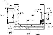
返回到图1,在第1液晶面板3的第1透光性基板21的伸出部24边端,例如使用ACF来连接作为具有挠性的布线基板之第1FPC基板51。第1FPC基板51在组装液晶显示装置1时,如箭头F所示地进行弯折使之卷合到壳体2的一边,配置于第1液晶面板3的显示面C相反侧的壳体2表面上。另外,在第2液晶面板4的第1透光性基板31的伸出部34边端上,例如使用ACF来连接作为具有挠性的布线基板之第2FPC基板52。对于这些第1FPC基板51及第2FPC基板52,将在下面进行具体说明。Returning to FIG. 1, the
接着,壳体2具有第1收置空间61和第2收置空间62。第1收置空间61,在图2中,设置于作为画出箭头A一侧的壳体2的第1面2a侧。该第1收置空间61是形成于壳体2内侧的空间,并且在该空间内收置第1液晶面板3及第1照明装置5。另外,第2收置空间62设置于作为画出箭头B一侧的壳体2的第2面2b侧。该第2收置空间62是形成于壳体2内侧的空间,并且在该空间内收置第2液晶面板4及第2照明装置6。Next, the casing 2 has a
当组装图1的液晶显示装置1时,首先将第1照明装置5、第1液晶面板3、第2照明装置6及第2液晶面板4,如图2所示安装到壳体2中。当进行该安装时,在图1中将第1照明装置5收置到第1收置空间61中之后,用粘接片19a对第1照明装置5和壳体2粘贴第1液晶面板3。此时,第1液晶面板3和第1照明装置5利用第1收置空间61而被限制图2的左右方向及纸面垂直方向的位置,因此总是定位于壳体2内的一定位置上。When assembling the liquid
接着,在图1中将第2照明装置6收置到第2收置空间62中之后,用粘接片19b对第2照明装置6和壳体2粘贴第2液晶面板4。此时,第2液晶面板4和第2照明装置6利用第2收置空间62而被限制图2的左右方向及纸面垂直方向的位置,因而总是定位于壳体2内的一定位置上。Next, after storing the
接着,在图1中,被第1FPC基板51如箭头F所示进行弯折,使之卷合壳体2的端边。然后,弯折后的第1FPC基板51被移动到第1液晶面板3的显示面C相反侧,也就是壳体2的第2面2b的表面上。如上所述,图2所示的液晶显示装置1就得以形成。Next, in FIG. 1 , the
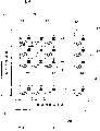
下面,对于本实施方式中作为用于液晶显示装置的布线基板之FPC基板,进行详细说明。图5(a)是从箭头A方向平面看到图1的第1FPC基板51的附图。另外,图5(b)是沿着图5(a)G-G线的第1FPC基板51的剖面图。Next, an FPC board serving as a wiring board used in a liquid crystal display device in this embodiment will be described in detail. FIG. 5( a ) is a plan view of the
第1FPC基板51例如以由聚酰亚胺或聚酯等构成的膜作为基体材料来形成,并且弯折性优良。该第1FPC基板51在如图1的箭头F那样进行了弯折时,具有与壳体2对面的表面S1和作为其相反面的表面S2。S1是进行弯折而成为内侧的面,S2是进行弯折而成为外侧的面。The
在本实施方式中,第1FPC基板51如图5(b)所示具有下述结构,即在由聚酰亚胺或聚酯等构成的基底膜54表面上形成导体55,再在导体55之上例如形成覆盖层和抗蚀剂层等之类的保护膜56。这些导体55和保护膜56,分别形成到基底膜54两侧的表面上。也就是说,本实施方式的第1FPC基板51其剖面具有2层的布线结构。因而,导体55形成于表面S1及表面S2的各自上,并且根据需要利用通孔,使这些导体55进行电导通。In this embodiment, the
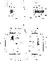
如图5(a)所示,第1FPC基板51具有电路形成部51a、弯折部51b、输入用端子51c、输出用端子51d及LED基板用端子51e。电路形成部51a是在图5(a)中用斜线所示的区域,并且是形成电子电路及为其附带的布线的部分。该电路形成部51a在将第1FPC基板51如图1的箭头F那样进行了弯折时,如图6(a)所示,配置于壳体2的第2收置空间62周围。因此,电路形成部51a如图5(a)那样,平面看上去形成为将开口部57包围的框状。该开口部57的宽度t1如图6(a)所示,按和壳体2两个侧面间的宽度t2大致相同或者比其稍大的宽度来形成。在此后的说明中,有时将夹着该开口部57的一方的电路形成部称为第1电路形成部51a′,将另一方的电路形成部称为第2电路形成部51a″。As shown in FIG. 5(a), the
在图5(a)中,第1电路形成部51a′具有弯曲部分63,可以在该弯曲部分63的位置上进行弯折。而且,在弯曲部分63的开口部57侧端部,设置缺口64。该第1电路形成部51a′如同图6(b)中用箭头J1所示,沿着壳体2的侧面2c向附图的下方进行弯折。然后,弯折后的第1电路形成部51a′的面例如采用双面胶带等之类的粘接部件68,粘接到壳体2的侧面2c上。在表示第1电路形成部51a′的弯曲部分63剖面的图5(b)中,如同保护膜56在没有施加斜线的状态下所描绘的那样,保护膜56没有在弯曲部分63上进行设置。在本实施方式中,如图5(a)所示,按和缺口64基本相同的宽度,设置不形成保护膜56的区域。In FIG. 5( a ), the first
这样,由于在第1电路形成部51a′的弯曲部分63的开口部57侧的端部,形成缺口64,因而可以正确确定该弯曲部分63的位置。另外,在本实施方式中如上所述,由于不在弯曲部分63上的形成保护膜56,因而可以使弯曲部分63处的基板的厚度变薄,而且能够降低该部分的刚性,因此能够将第1电路形成部51a′容易弯折。In this way, since the
另一方面,在图5(a)中,第2电路形成部51a″具有弯曲部分66,可以在该弯曲部分66的位置进行弯折。而且,在弯曲部分66的开口部57侧的端部,设置缺口67。该第2电路形成部51a″如同图6(b)中用箭头J2所示,沿着壳体2的侧面2c向附图的下方进行弯折。然后,弯折后的第2电路形成部51a″的面例如采用双面胶带等之类的粘接部件68,粘接到壳体2的侧面2c上。On the other hand, in FIG. 5(a), the second
这样,在图5(a)中,由于在第2电路形成部51a″的弯曲部分66的开口部57侧的端部,设置缺口67,因而可以正确确定该弯曲部分66的位置。另外,在本实施方式中如上所述,对于弯曲部分66,也和第1电路形成部51a′侧的弯曲部分63相同地不形成保护膜56。这样一来,就可以使弯曲部分66处的基板的厚度变薄,而且能够降低该部分的刚性,因此能够将第2电路形成部51a″容易弯折。In this way, in FIG. 5( a), since the end portion of the
电路形成部51a是形成电子电路和布线的部分,但是作为其一部分的第1电路形成部51a′及第2电路形成部51a″可以主要作为对电路形成部51a的输入用端子51c侧的电路形成部分和输出用端子51d侧的电路形成部分进行电连接的要件,来发挥作用。因而,在这些第1电路形成部51a′及第2电路形成部51a″上,可以只设置对输入用端子51c侧和输出用端子51d侧进行连接的布线。另外,在第1电路形成部51a′及第2电路形成部51a″上除布线之外,还可以安装IC等之类的电子构件。The
接着,在设置有输入用端子51c一侧的电路形成部51a的表面(弯折时成为外侧的面)S2上,安装多个电子构件35a。另外,同样在弯折部51b的表面(弯折时成为内侧的面)S1上,安装多个电子构件35b。这些电子构件35a、35b用来对图1的第1液晶面板3及/或第2液晶面板4进行驱动,例如可以考虑电阻、线圈、电容器及电源IC等。另外,在设置了输入用端子51c一侧的电路形成部51a的成为外侧的表面S2上,设置LED基板用端子51e。对该LED基板用端子51e,例如通过焊接来连接图1的LED基板15。然后,再在图5(a)的电路形成部51a表里两侧的表面上,通过构图来形成多条布线,该多条布线用来连接各电子构件35a、35b和端子,构成电路。Next, a plurality of
接着,弯折部51b是将第1FPC基板51如图1的箭头F那样弯折时产生弯曲的部分。如图5(b)所示,在作为该弯折部51b内侧的表面S1侧,设置不形成保护膜56的保护膜未形成部69。该保护膜未形成部69设置成,沿着图5(b)的纸面垂直方向笔直延伸,使弯折部51b的厚度变薄而易于弯折。在本实施方式中,保护膜未形成部69设置了一处。但是,该保护膜未形成部69也可以设置于多个部位。另外,在本实施方式中,虽然保护膜未形成部69设置到弯曲地成为内侧的表面S1侧,但是也可以将其设置到进行弯折而成为外侧的表面S2侧。Next, the
接着,在图5(a)中,输入用端子51c设置成,向和电路形成部51a的弯折部51b相反侧的端边突出。在该输入用端子51c上,连接外部的输入用设备(例如,便携式电话机等之类的电子设备的控制电路)和外部电源等。另外,输出用端子51d如图1所示,例如使用ACF连接于第1液晶面板3的伸出部24上。向输出用端子51d所传送的信号通过第1液晶面板3的外部连接用端子,传送给驱动用IC26。Next, in FIG. 5(a), the
另外,在图5(a)中,在作为电路形成部51a外侧的表面S2上且在输入用端子51c的附近,设置连接器58。在该连接器58上,连接图1的第2FPC基板52的下述输入用端子52a。还有,在第1FPC基板51上,也可以代替连接器58而设置端子。这种情况下,可以把该端子和第2FPC基板52的输入用端子52a,例如通过焊接来连接两个端子。Moreover, in FIG.5(a), the
接着,在图1中,在第2液晶面板4的第1透光性基板31的伸出部34边端,例如使用ACF连接作为具有挠性的布线基板之第2FPC基板52。该第2FPC基板52和第1FPC基板51相同,例如以由聚酰亚胺或聚酯等构成的膜作为基体材料来形成。Next, in FIG. 1, the
在该第2FPC基板52上,形成输入用端子52a。该输入用端子52a与设置于第1FPC基板51上的连接器58进行连接。借此,通过第1FPC基板51和第2FPC基板52,来电连接第1液晶面板3和第2液晶面板4。而且,驱动第1液晶面板3及第2液晶面板4所用的信号和电力通过第2FPC基板52及第1FPC基板51,从输入用设备和外部电源供给。On this
此外,在图1所示的结构的液晶显示装置1中,在将第1FPC基板51如箭头F那样进行了弯折时,需要把该第1FPC基板51配置到不妨碍第2液晶面板4的显示的位置上。但是,以往,要使液晶显示装置小型化,则难以较大确保该液晶显示装置在壳体2的区域内配置FPC基板的面积。为此,不得不使FPC基板向壳体的外侧伸出地进行设置,因此难以较小形成液晶显示装置的整体。In addition, in the liquid
针对这种问题,在本实施方式中,如图6(b)所示,在弯曲部分63处将第1电路形成部51a′向箭头J1的方向进行弯折,以使其表面与壳体2的侧面2c对向。另外,同样在弯曲部分66处将第2电路形成部51a″向箭头J2的方向进行弯折,以使其表面与壳体2的侧面2c对向。这样,如果将第1FPC基板51的电路形成部51a一部分配置到壳体2的侧面2c上,则即便在为了使液晶显示装置1小型化而较小形成壳体2时,也可以较大确保第1FPC基板51的电路形成部51a的面积,因此,能够将具有该第1FPC基板51的液晶显示装置1形成为小型。另外,反之还可以增大第1FPC基板51的实际面积,在该第1FPC基板51的电路形成部51a上形成较大的电路。To solve this problem, in this embodiment, as shown in FIG. The
接着,采用图7,来说明在图1的液晶显示装置1的第1液晶面板3上安装作为布线基板的第1FPC基板51并再把它们对壳体2进行安装的方法。首先,在图7的工艺P1中,对图1的第1液晶面板3连接第1FPC基板51。此时,图5(a)所示的第1FPC基板51的输出用端子51d对图1的第1液晶面板3的伸出部24上所形成的外部连接用端子(未图示),使用ACF进行电连接。Next, a method of mounting the
接着,在图7的工艺P2中如图2所示,将第1液晶面板3及第1照明装置5收置到壳体2的第1收置空间61内。另外,同样将第2液晶面板4及第2照明装置6收置到壳体2的第2收置空间62内。接着,在图7的工艺P3中,执行用来组装液晶显示装置1的第1FPC基板51的1次弯折工艺。具体而言,将图1的第1FPC基板51在弯折部51b处,如箭头F所示地进行弯折。此时,第1FPC基板51卷入壳体2的一边地弯折,配置到作为第1液晶面板3的显示面C相反侧的壳体2的第2面2b上。Next, in process P2 of FIG. 7 , as shown in FIG. 2 , the first
接着,在图7的工艺P4中,执行2次弯折工艺,该2次弯折工艺用来在平面看壳体2时在该壳体2的区域内收置第1FPC51。具体而言,将图5(a)所示的第1电路形成部51a′,沿着弯曲部分63向图5(a)的里侧进行弯折。此时,第1电路形成部51a′向图6(b)中用箭头J1所示的方向进行弯折,并且其表面与壳体2的侧面2c对向。另外,同样将图5(a)所示的第2电路形成部51a″,沿着弯曲部分66向图5(a)的里侧进行弯折。此时,第2电路形成部51a″向图6(b)中用箭头J2所示的方向进行弯折,并且其表面与壳体2的侧面2c对向。Next, in the process P4 of FIG. 7 , a secondary bending process is performed to house the
接着,在图7的工艺P5中如图6(b)所示,将第1FPC基极51的第1电路形成部51a′及第2电路形成部51a″,例如使用粘接部件68等,粘接到壳体2的侧面2c上。Next, in the process P5 of FIG. 7, as shown in FIG. 6(b), the first
接着,在图7的工艺P6中如图6(a)所示,将第2FPC基板52的输入用端子52a插入第1FPC基板51的连接器58中。借此,图1的第1液晶面板3和第2液晶面板4通过第1FPC基板51和第2FPC基板52进行电连接。通过上面的工艺,就能在包括于液晶显示装置1中的第1液晶面板3上安装第1FPC基板51,液晶显示装置1得以完成。Next, in process P6 of FIG. 7 , as shown in FIG. 6( a ), the input terminal 52 a of the
如上所述,在本实施方式所涉及的布线基板安装方法中,在图7的工艺P4中,如图6(b)所示,在弯曲部分63处将第1电路形成部51a′向箭头J1的方向进行弯折,以使其表面与壳体2的侧面2c对向。另外,同样在弯曲部分66处将第2电路形成部51a″向箭头J2的方向弯折,以使其表面与壳体2的侧面2c对向。这样,如果将第1FPC基板51的电路形成部51a一部分配置到壳体2的侧面2c上,则即便在为了使液晶显示装置1小型化而较小形成壳体2时,也可以较大确保第1FPC基板51的电路形成部51a的面积,因此,能够将具有该第1FPC基板51的液晶显示装置1形成为小型。另外,反之还可以增大第1FPC基板51的实际面积,在该第1FPC基板51的电路形成部51a上形成较大的电路。As described above, in the wiring board mounting method according to this embodiment, in the process P4 of FIG. 7 , as shown in FIG. The direction is bent so that its surface faces the
(电光装置的第2实施方式)(Second embodiment of electro-optical device)
下面,说明本发明所涉及的电光装置其他实施方式。本实施方式的说明也以液晶显示装置为例来进行。Next, other embodiments of the electro-optical device according to the present invention will be described. The description of the present embodiment is also performed by taking a liquid crystal display device as an example.
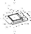
图8表示出,作为本发明所涉及的电光装置的其他实施方式的液晶显示装置71。本实施方式和第1实施方式的不同之处为,以下方面。在第1实施方式中如图1所示,第2收置空间62是形成于壳体2内侧的空间,并且设置于作为画出箭头B一侧的壳体2的第2面(也就是,安装第2液晶面板74一侧的面)2b侧。相对于此,在本实施方式中如图8所示,在壳体72的画出箭头B一侧的面,也就是第2面72b上形成从该第2面72b突出的框状部93,并且在该框状部93的内侧形成第2收置空间92。下面,以和图1的液晶显示装置1的不同之处为中心,来说明图8的液晶显示装置71。FIG. 8 shows a liquid
在图8的液晶显示装置71中,第1FPC基板81的结构可以和图5所示的第1FPC基板51相同,并且在本实施方式中设为是其相同的结构。另外,图8中第2FPC基板82、第1液晶面板73、第2液晶面板74及第2照明装置76的结构,可以分别和图1所示的第2FPC基板52、第1液晶面板3、第2液晶面板4及第2照明装置6相同,并且在本实施方式中设为是其相同的结构。还有,在图5(a)及图5(b)所示的要件和图8所示的要件相同时,用相同的符号来表示它们。In the liquid
在图8中,在第2收置空间92内收置第2液晶面板74及第2照明装置76。该第2收置空间92按和下述总厚度大致相同的高度来形成,该总厚度是将第2液晶面板74的厚度和第2照明装置76的厚度合起来后的厚度。另外,形成第2收置空间92的框状部93之中的相互对向的框状部之间的距离t4,形成得比壳体72两个侧面间的宽度t3小。In FIG. 8 , the second
在上述框状部93之中的设置第2FPC基板82一侧的一边,形成开放部93a,该开放部93a的面比余下的突出部低,但是比第2面72b高,或者是和第2面72b相同的高度。该开放部93a为将形成第2收置空间92的框状部93的一边切除而开放的形状。另外,开放部93a为了使第2FPC基板82向外部延伸,按大于等于第2FPC基板82宽度的宽度来形成。另外,开放部93a优选的是,按下述高度来形成,该高度为在将第2液晶面板74及第2照明装置76收置到第2收置空间92内时,开放部93a的底面93b不接触到第2FPC基板82的高度。借此,第2FPC基板82在将第2液晶面板74及第2照明装置76收置到第2收置空间92内时,可以通过开放部93a向第2收置空间92外,直地延伸出来。On one side of the frame-shaped
第1FPC基板81的第2电路形成部51a″在弯曲部分66处向附图的下方进行弯折,以对壳体72的侧面2c使其表面对向。然后,弯折后的第2电路形成部51a″例如使用双面胶带等之类的粘接部件68,粘接到壳体72的侧面2c上。还有,虽然未进行图示,但是第1FPC基板81另一方的一侧的第1电路形成部51a′也同样在弯曲部分63处进行弯折使之与壳体72的侧面2c对向,并且进行粘接。The second
根据图8的实施方式,在弯曲部分63、66处,第1FPC基板81的第1电路形成部51a′及第2电路形成部51a″向附图的下方向进行弯折,以使其表面与壳体72的侧面2c对向。这样,如果将第1FPC基板81的电路形成部51a的一部分配置到壳体72的侧面2c上,则即便在为了使液晶显示装置71小型化而较小形成壳体72时,也可以较大确保第1FPC基板81的电路形成部51a的面积,因此,能够将具有该第1FPC基板81的液晶显示装置71形成为小型。另外,反之还可以增大第1FPC基板81的实际面积,在该第1FPC基板81的电路形成部51a上形成较大的电路。According to the embodiment of FIG. 8, at the bending
(电光装置的第3实施方式)(Third embodiment of electro-optic device)
下面,说明本发明所涉及的电光装置另一其他实施方式。本实施方式的说明也以液晶显示装置为例来进行,并且和第1实施方式及第2实施方式的情形相同的符号表示相同的要件。Next, another embodiment of the electro-optical device according to the present invention will be described. The description of this embodiment is also performed using a liquid crystal display device as an example, and the same reference numerals as in the first embodiment and the second embodiment denote the same requirements.
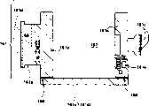
图9表示出,作为本发明所涉及的电光装置其他实施方式的液晶显示装置101。另外,图10是从箭头B方向平面看到图9的第1FPC基板111的附图。还有,弯折部111b以展开后的状态来表示。另外,虽然图10是相当于图5(a)的附图,但是图10所示的第1FPC基板111的状态为,使图5(a)的第1FPC基板51只进行了180°的面内旋转。这是为了使图10对应于图9所示的状态。FIG. 9 shows a liquid
在上述的第2实施方式中如图8所示,在壳体72的第2面72b上形成从该第2面72b突出的框状部93,并且该框状部93之中的相互对向的框状部之间的距离t4形成得比壳体72的宽度t3小。相对于此,在本实施方式中如图9所示,框状部123之中的相互对向的框状部之间的距离t6和壳体102的宽度t5按相同的尺寸来形成。下面,以和图8的液晶显示装置71的不同之处为中心,来说明图9的液晶显示装置101。In the above-mentioned second embodiment, as shown in FIG. 8 , the frame-shaped
在图9的液晶显示装置101中,第2FPC基板112、第1液晶面板103、第2液晶面板104及第2照明装置106的结构,可以分别和图8所示的第2FPC基板82、第1液晶面板73、第2液晶面板74及第2照明装置76相同,并且在本实施方式中设为是其相同的结构。另外,图9的壳体102除了框状部的形状之外,其构造可以和图8的壳体72相同,并且在本实施方式中设为是其相同的结构。另外,第1FPC基板111除电路形成部的形状,特别是除第1电路形成部51a′及第2电路形成部51a″的形状之外,其构造可以和图8所示的第1FPC基板81还有图5(a)及图5(b)所示的第1FPC基板51相同。还有,在图9及图10中,符号111b表示第1FPC基板111的弯折部,符号111c表示输入用端子,符号111d表示输出用端子,符号69表示保护膜未形成部。In the liquid
首先,在图9中,框状部123之中相互对向的框状部之间的距离t6和壳体102两个侧面间的宽度t5相同。也就是说,壳体102的侧面102c成为包括框状部123侧面的面。而且,形成框状部123的区域的壳体102的侧面102c的高度t8与此外区域的壳体102的侧面102c的高度t7相比,变得高。First, in FIG. 9 , the distance t6 between the frame-shaped
接着,在第1FPC基板111上如图10所示,设置使第1电路形成部111a′向开口部117内侧突出的形状的突出部110a。包括该突出部110a在内的第1电路形成部111a′的宽度t9和图9所示壳体102的侧面102c对应部分的高度t8相同,或者比其稍小。Next, on the
另外,在夹着图10的开口部117与第1电路形成部111a′对向的第2电路形成部111a″上,设置向开口部117内侧突出的形状的突出部110b。包括该突出部110b在内的第2电路形成部111a″的宽度t10和图9所示的壳体102的侧面102c对应部分的高度t8相同,或者比其稍小。In addition, on the second circuit forming part 111a'' facing the first circuit forming part 111a' across the opening part 117 in FIG. The width t10 of the inner second circuit forming portion 111a" is the same as or slightly smaller than the height t8 of the corresponding portion of the
上述结构的第1FPC基板111如图9所示,与设置于液晶显示装置101内的第1液晶面板103连接。此时,第1FPC基板111的第2电路形成部111a″在弯曲部分126处沿着壳体102的侧面102c向附图的下方进行弯折。另外,第2电路形成部111a″的突出部110b在第2电路形成部111a″的整体被弯折的状态时,以向上方抬高的状态配置到框状部123的侧面上。然后,第2电路形成部111a″例如使用双面胶带等之类的粘接部件128,粘接到壳体102的侧面102c上。还有,图10的第1电路形成部111a′及其突出部110a虽然在图9中没有图示,但是对于这些第1电路形成部111a′及其突出部110a,也和第2电路形成部111a″相同地沿着侧面102c弯折,并且进行粘接。The
根据图9的实施方式,作为第1FPC基板111的电路形成部111a一部分之第1电路形成部111a′及第2电路形成部111a″向附图的下方进行弯折,使之与壳体102的侧面102c对向。这样,如果将第1FPC基板111的电路形成部111a一部分配置到壳体102的侧面102c上,则即便在为了使液晶显示装置101小型化而较小地形成壳体102时,也可以较大确保第1FPC基板111的电路形成部111a的面积,因此,可以将具有该第1FPC基板111的液晶显示装置101形成为小型。另外,反之还可以增大第1FPC基板111的实际面积,在该第1FPC基板111的电路形成部111a上形成较大的电路。According to the embodiment of FIG. 9, the first circuit forming part 111a' and the second circuit forming part 111a" which are a part of the circuit forming part 111a of the
另外,对于壳体102,框状部123之中的相互对向的框状部之间的距离t6和壳体102的宽度t5按相同的尺寸来形成。借此,由于壳体102的侧面102c成为包括框状部123侧面的面,因而可以扩大该侧面102c的面积。其结果为,在壳体102两侧的侧面102c上,可以分别配置图10的设置有突出部110a的第1电路形成部111a′和设置有突出部110b的第2电路形成部111a″。因为这些第1电路形成部111a′和第2电路形成部111a″分别可以通过设置突出部110a及突出部110b来扩大形成电路的面积,所以能够形成较大的电路。In addition, in the
(电光装置的第4实施方式)(Fourth embodiment of electro-optical device)
下面,说明本发明所涉及的电光装置的另一其他实施方式。本实施方式的说明也以液晶显示装置为例来进行,并且和第1实施方式、第2实施方式及第3实施方式的情形相同的符号表示相同的要件。Next, another embodiment of the electro-optical device according to the present invention will be described. The description of this embodiment is also performed using a liquid crystal display device as an example, and the same symbols as those in the first embodiment, the second embodiment, and the third embodiment denote the same requirements.
图11表示出,作为本发明所涉及的电光装置的其他实施方式的液晶显示装置151。另外,图12是从箭头B方向平面看图11的第1FPC基板161的附图。还有,弯折部161b表示出展开后的状态。另外,虽然图12是相当于图5(a)的附图,但是图12所示的第1FPC基板161的状态为,使图5(a)的第1FPC基板51只进行了180°的面内旋转。这是为了使图12对应于图11所示的状态。FIG. 11 shows a liquid crystal display device 151 as another embodiment of the electro-optical device according to the present invention. In addition, FIG. 12 is a plan view of the
在第1实施方式中如图5(a)所示,第1FPC基板51的电路形成部51a形成为具有开口部57的框状,并且在夹着开口部57的附图左右两侧,设置输入用端子51c侧的电路形成部和输出用端子51d侧的电路形成部,在附图上下两端,设置将它们连接起来的第1电路形成部51a′和第2电路形成部51a″。而且,第1电路形成部51a′和第2电路形成部51a″如图6(b)所示,分别以使它们的表面与壳体2的侧面2c对向的方式进行弯折。In the first embodiment, as shown in FIG. 5(a), the
相对于此,在本实施方式中如图12所示,第1FPC基板161的电路形成部161a形成为大致コ字状,该大致コ字状是将FPC基板开放部157包围的形状。在该コ字形状中的与开放的部分对向的部分上,设置第2电路形成部161a″。而且,该第2电路形成部161a″在图11中,以与壳体152的一个侧面152c对向的方式进行弯折。下面,以和图6的液晶显示装置1的不同之处为中心,来说明图11的液晶显示装置151。On the other hand, in this embodiment, as shown in FIG. 12 , the
在图11的液晶显示装置151中,第2FPC基板162、第1液晶面板153、第2液晶面板154及第2照明装置156的结构,可以分别和图1所示的第2FPC基板52、第1液晶面板3、第2液晶面板4及第2照明装置6相同,并且在本实施方式中设为是其相同的结构。另外,图12的第1FPC基板161除电路形成部的形状之外,其构造可以和图5所示的第1FPC基板51相同,并且在本实施方式中设为是其相同的结构。In the liquid crystal display device 151 of Fig. 11, the structure of the 2nd FPC substrate 162, the 1st liquid crystal panel 153, the 2nd liquid crystal panel 154 and the 2nd illuminating device 156 can be respectively and the
在图12中,第1FPC基板161具有电路形成部161a、弯折部161b、输入用端子161c、输出用端子161d及LED基板用端子161e。电路形成部161a是在图12中用斜线所示的区域。第1FPC基板161如图11所示,连接到箭头A侧所配置的第1液晶面板153上。再者,第1FPC基板161在弯折部161b处,使之卷入壳体152的端边地进行弯折,配置到箭头B侧,也就是壳体152的第2面152b的表面上。In FIG. 12, the 1st FPC board|
在图12中,第1FPC基板161的电路形成部161a平面看上去,形成为将FPC基板开放部157包围的大致コ字状。电路形成部161a中的与因FPC基板开放部157而开放的部分对向的部分是第2电路形成部161a″。该第2电路形成部161a″如图11所示,在弯曲部分166处向附图的下方进行弯折,以对壳体152的一个侧面152c使其表面对向。而且,弯折后的第2电路形成部161a″例如使用双面胶带等之类的粘接部件168,粘接到壳体152的侧面152c上。In FIG. 12 , the
根据图11的实施方式,在弯曲部分166处,作为第1FPC基板161的电路形成部161a一部分的第2电路形成部161a″向附图的下方进行弯折,以使其表面与壳体152的一个侧面152c对向。这样,如果将第2电路形成部161a″配置到壳体152的侧面152c上,则即便在为了使液晶显示装置151小型化而较小形成壳体152时,也可以较大确保第1FPC基板161的电路形成部161a的面积,因此,可以将具有该第1FPC基板161的液晶显示装置151形成为小型。另外,反之还可以增大第1FPC基板161的实际面积,在该第1FPC基板161的电路形成部161a上形成较大的电路。According to the embodiment of FIG. 11 , at the
(电光装置的第5实施方式)(Fifth Embodiment of Electro-optic Device)
下面,说明本发明所涉及的电光装置另一其他实施方式。本实施方式的说明也以液晶显示装置为例来进行,并且和第1实施方式、第2实施方式、第3实施方式及第4实施方式的情形相同的符号表示相同的要件。Next, another embodiment of the electro-optical device according to the present invention will be described. The description of this embodiment is also performed using a liquid crystal display device as an example, and the same reference numerals as in the first embodiment, the second embodiment, the third embodiment, and the fourth embodiment denote the same requirements.
图13表示出,作为本发明所涉及的电光装置另一其他实施方式的液晶显示装置171。另外,图14是从箭头B方向平面看到图13的第1FPC基板181的附图。还有,弯折部181b表示出展开后的状态。在图6所示的第1实施方式中,以使第1电路形成部51a′及第2电路形成部51a″的内侧表面S1与壳体2的侧面2c分别对向的方式设置第1FPC基板51。相对于此,在本实施方式中如图13所示,除了侧面172c上之外,还在壳体172的第2面172b上的、而且为第2液晶面板174和侧面172c之间的平面区域172d(用斜线所示的区域)上,分别设置第1电路形成部181a′及第2电路形成部181a″。下面,以和图6的液晶显示装置1的不同之处为中心,来说明图13的液晶显示装置171。FIG. 13 shows a liquid
在图13的液晶显示装置171中,壳体172、第2FPC基板182、第1液晶面板173、第2液晶面板174及第2照明装置176的结构,可以分别和图1所示的壳体2、第2FPC基板52、第1液晶面板3、第2液晶面板4及第2照明装置6相同,并且在本实施方式中设为是其相同的结构。另外,图14的第1FPC基板181除了电路形成部的形状之外,其构造可以和图5的第1FPC基板51相同,并且在本实施方式中设为是其相同的结构。In the liquid
在图14中,第1FPC基板181具有电路形成部181a、弯折部181b、输入用端子181c、输出用端子181d及LED基板用端子181e。电路形成部181a是在图14中用斜线所示的区域。第1FPC基板181如图13所示,连接到箭头A侧所配置的第1液晶面板173上。再者,第1FPC基板181在弯折部181b处以卷进壳体172的端边的方式进行弯折,配置到箭头B侧,也就是壳体172的第2面172b表面上。In FIG. 14, the 1st FPC board|
第1FPC基板181如图14所示,平面看上去形成为将开口部177包围的框状。在第1FPC基板181上,夹着开口部177的一方的电路形成部是第1电路形成部181a′,另一方的电路形成部是第2电路形成部181a″。As shown in FIG. 14 , the
第1电路形成部181a′具有下述弯曲部分183,可以在该弯曲部分183的位置将第1电路形成部181a′弯折,上述弯曲部分是沿着通过第1电路形成部181a’的大致中心的假想线X0所设置的线状区域。该弯曲部分183的两个端部是没有图5的保护膜56而只由基底膜54构成的厚度较薄的部分,并且在这些厚度较薄的部分之间设置从作为内侧的表面S1一直贯通到作为外侧的表面S2的细长空间的、所谓的缝隙184。这样,由于在弯曲部分183上设置缝隙184,因而可以在弯曲部分183处将第1FPC基板181更为容易地弯折。还有,在本实施方式中,虽然沿着弯曲部分183设置了一条缝隙184,但是缝隙184只要确保了可在弯曲部分183上设置必要布线的区域,也可以沿着弯曲部分183设置二条或二条以上。另外,缝隙184只要第1FPC基板181可以在弯曲部分183处容易地弯折,也可以不设置。The first
另一方面,第2电路形成部181a″具有和弯曲部分184相同结构的弯曲部分186,可以在该弯曲部分186的位置进行弯折。由于在该弯曲部分186上也设置从内侧表面S1一直贯通到外侧表面S2的缝隙187,因而可以在该弯曲部分186处将第1FPC基板181更为容易地弯折。还有,在本实施方式中,虽然沿着弯曲部分186设置了一条缝隙187,但是缝隙187只要确保了可在弯曲部分186上设置必要布线的区域,也可以沿着弯曲部分186设置二条或二条以上。另外,缝隙187只要第1FPC基板181可以在弯曲部分186处容易地弯折,也可以不设置。On the other hand, the second
在本实施方式的第1FPC基板181上,第1电路形成部181a′的弯曲部分183和第2电路形成部181a″的弯曲部分186之间的间隔t14按和图13所示的壳体172两个侧面间的宽度t11大致相同或者比其稍大的间隔,来形成。另外,开口部177的宽度t13按和图13所示的壳体172的第2收置空间192的宽度t12大致相同或者比其稍大的宽度,来形成。In the
在图13中,第2电路形成部181a″中的弯曲部分186和开口部177之间的部分配置于壳体172的第2面172b上的、而且为第2液晶面板174和侧面172c之间的平面区域(也就是,用斜线所示的区域)172d上。该平面区域172d是在壳体172中的安装第2液晶面板174一侧的面上与安装第2液晶面板174的区域相邻的旁边区域。另外,第2电路形成部181a″中的比弯曲部分186靠外侧的部分,沿着壳体172的侧面172c地向附图的下方进行弯折。而且,弯折后的第2电路形成部181a″的面例如使用双面胶带等之类的粘接部件188,粘接到壳体172的侧面172c上。In FIG. 13 , the portion between the
另一方面,第1电路形成部181a′中的弯曲部分183和开口部177之间的部分配置于壳体172的第2面172b上的而且为第2液晶面板174和侧面172c之间的平面区域172d(用斜线所示的部分)上。还有,对于图14的第1电路形成部181a′中的比弯曲部分183靠外侧的部分,虽然在图13中未图示,但是和第2电路形成部181a″相同,沿着侧面172c进行弯折,并且进行粘接。On the other hand, the portion between the
在图13的实施方式中,在弯曲部分186处,第2电路形成部181a″,以使其表面与壳体172的侧面172c对向的方式弯折。另外,同样在弯曲部分183处,第1电路形成部181a′,以使其表面与壳体172的侧面172c对向的方式进行弯折。这样,如果将第1FPC基板181的电路形成部181a配置到壳体172的侧面172c上,则即便在为了使液晶显示装置171小型化而较小形成壳体172时,也可以较大确保第1FPC基板171的电路形成部181a的面积,因此,能够将具有该第1FPC基板181的液晶显示装置171形成为小型。另外,反之还可以增大第1FPC基板181的实际面积,在该第1FPC基板181的电路形成部181a上形成较大的电路。In the embodiment of FIG. 13 , at the
另外,在本实施方式中,还在壳体172的第2面172b上的、而且为第2液晶面板174和侧面172c之间的平面区域172d上,设置作为电路形成部181a的一部分的第1电路形成部181a′和第2电路形成部181a″。其结果为,与只把第1电路形成部181a′和第2电路形成部181a″设置到壳体172的侧面172c上的情形相比,可以扩大电路形成部181a的面积,其结果能够形成更大的电路。In addition, in the present embodiment, the first
(电光装置的第6实施方式)(Sixth embodiment of electro-optic device)
下面,说明本发明所涉及的电光装置的另一其他实施方式。本实施方式的说明也以液晶显示装置为例来进行,并且和第1实施方式、第2实施方式、第3实施方式、第4实施方式及第5实施方式的情形相同的符号表示相同的要件。Next, another embodiment of the electro-optical device according to the present invention will be described. The description of this embodiment is also performed using a liquid crystal display device as an example, and the same symbols as in the first embodiment, the second embodiment, the third embodiment, the fourth embodiment, and the fifth embodiment represent the same requirements. .
图15表示出,作为本发明所涉及的电光装置其他实施方式的液晶显示装置201。另外,图16是从箭头B方向平面看图15的第1FPC基板211的附图。还有,弯折部211b表示出展开后的状态。在第5实施方式中如图14所示,第1FPC基板181的电路形成部181a形成为将开口部177包围的框状,并且在夹着开口部177的附图左右两侧,有输入用端子181c侧的电路形成部和输出用端子181d侧的电路形成部,在附图上下两侧,设置将这些电路形成部连接起来的第1电路形成部181a′和第2电路形成部181a″。而且,第1电路形成部181a′和第2电路形成部181a″如图13所示分别设置为,其表面的一部分与壳体172的侧面172c对向,并且其表面的另一部分与壳体172的第2面172b上的、且为第2液晶面板174和侧面172c之间的平面区域172d对向。FIG. 15 shows a liquid crystal display device 201 as another embodiment of the electro-optical device according to the present invention. In addition, FIG. 16 is a plan view of the
相对于此,在本实施方式中如图16所示,第1FPC基板211的电路形成部211a形成为大致コ字状,该大致コ字状是将FPC基板开放部207包围的形状。在该コ字形状中的与开放的部分对向的部分上,设置第2电路形部211a″。而且,该第2电路形成部211a″在图15中设置为,分别与壳体202的侧面202c以及壳体202的第2面(也就是,安装第2液晶面板204一侧的面)202b上的且为第2液晶面板204和侧面202c之间的平面区域202d(用斜线所示的区域)对向。下面,以和图13的液晶显示装置171的不同之处为中心,来说明图15的液晶显示装置201。On the other hand, in this embodiment, as shown in FIG. 16 , the
在图15的液晶显示装置201中,壳体202、第2FPC基板212、第1液晶面板203、第2液晶面板204及第2照明装置206的结构,可以分别和图13所示的壳体172、第2FPC基板182、第1液晶面板173、第2液晶面板174及第2照明装置176相同,并且在本实施方式中设为是其相同的结构。另外,图16的第1FPC基板211除电路形成部的形状之外,其构造可以和图14所示的第1FPC基板181相同,并且在本实施方式中设为是其相同的结构。In the liquid crystal display device 201 of Fig. 15, the structures of the casing 202, the second FPC substrate 212, the first liquid crystal panel 203, the second liquid crystal panel 204, and the second illuminating device 206 can be respectively the same as those of the
在图16中,第1FPC基板211具有电路形成部211a、弯折部211b、输入用端子211c、输出用端子211d及LED基板用端子211e。电路形成部211a是在图16中用斜线所示的区域。第1FPC基板211如图15所示,连接到箭头A侧所配置的第1液晶面板203上。再者,第1FPC基板211在弯折部211b处以卷进壳体202的端边的方式进行弯折,配置到箭头B侧,也就是壳体202的第2面202b的表面上。In FIG. 16, the 1st FPC board|
在图16中,第1FPC基板211的电路形成部211a平面看上去,形成为将FPC基板开放部207包围的大致コ字状。电路形成部211a中的与因FPC基板开放部207而开放的部分对向的部分是第2电路形成部211a″。In FIG. 16 , the
第2电路形成部211a″具有弯曲部分216,可以在该弯曲部分216的位置进行弯折。在该弯曲部分216上,设置从作为内侧的表面S1一直贯通到作为外侧的表面S2的细长空间的、所谓的缝隙217。这样,通过在弯曲部分216上设置缝隙217,就可以在弯曲部分216处将第1FPC基板211更为容易地弯折。还有,在本实施方式中,虽然沿着弯曲部分216设置1条缝隙217,但是缝隙217只要确保了可在弯曲部分216上设置必要布线的区域,也可以沿着弯曲部分216设置2条或2条以上。另外,缝隙217只要第1FPC基板211可以在弯曲部分216处容易地弯折,也可以不设置。The second
在图15中,第2电路形成部211a″中的弯曲部分216和开口部207之间的部分,配置于壳体202的第2面202b上的且为第2液晶面板204和侧面202c之间的平面区域202d(用斜线所示的区域)上。另外,第2电路形成部211a″中的比弯曲部分216靠外侧的部分沿着壳体202的侧面202c地向附图的下方进行弯折。而且,弯折后的第2电路形成部201a″的面例如使用双面胶带等之类的粘接部件218,粘接到壳体202的侧面202c上。In FIG. 15, the portion between the
在图15的实施方式中,在弯曲部分216处对第2电路形成部211a″进行弯折,以使其表面与壳体202的侧面202c对向。这样,如果将第1FPC基板211的电路形成部211a配置到壳体202的侧面202c上,则在即便为了使液晶显示装置201小型化而较小形成壳体202时,也可以较大确保第1FPC基板211的电路形成部211a的面积,因此,可以将具有该第1FPC基板211的液晶显示装置201形成为小型。另外,反之还可以增大第1FPC基板211的实际面积,在该第1FPC基板211的电路形成部211a上形成较大的电路。In the embodiment of FIG. 15, the second
另外,由于也在壳体202的第2面202b上的且为第2液晶面板204和侧面202c之间的平面区域202d上,设置作为电路形成部211a的一部分的第2电路形成部211a″,因而与只把第2电路形成部211a″设置到壳体202的侧面202c上的情形相比,可以扩大电路形成部211a的面积,能够形成更大的电路。In addition, since the second
(电光装置及布线基板安装方法的其他实施方式)(Other Embodiments of Electro-optic Device and Wiring Board Mounting Method)
上面,虽然列举最佳实施方式说明了本发明,但是本发明并不限定为该实施方式,而可以在技术方案所述的发明范围内进行各种改变。As mentioned above, although the present invention was described with reference to the best embodiment, the present invention is not limited to the embodiment, and various changes can be made within the scope of the invention described in the claims.
例如,在上述电光装置的实施方式中,在图1中示例出下述结构的液晶显示装置1,该结构为在第1FPC基板51上设置电路形成部51a,并将该电路形成部51a的一部分,以使其表面与壳体2的侧面2c对向的方式进行弯折。但是,本发明还包括将除电路形成部以外的区域弯折的结构。另外,本发明的结构也可以为,将第2FPC基板52,以使其表面与壳体2的侧面2c对向的方式弯折。另外,也可以在第1PFC基板51及第2FPC基板52双方的基板上设置弯曲部分,并以该弯曲部分为基准将这些基板51、52的一部分,以使其表面与壳体2的侧面2c对向的方式弯折。For example, in the above-mentioned embodiment of the electro-optic device, FIG. 1 exemplifies a liquid
另外,在上述电光装置的实施方式中,在图1中示例出使用下述2个液晶面板的结构的液晶显示装置1,该2个液晶面板一个是进行主要显示的第1液晶面板3,另一个是进行辅助显示的第2液晶面板4。但是,本发明也可以适用于使用1个液晶面板的液晶显示装置。In addition, in the above embodiment of the electro-optical device, FIG. 1 illustrates a liquid
另外,在上述电光装置的实施方式中,如图6(b)所示,将第1FPC基板51的电路形成部51a,使用粘接部件68粘接到壳体2的侧面2c上。也可以取而代之,设置覆盖壳体2的侧面2c的框体,利用该框体将第1FPC基板51的电路形成部51a按压于壳体2的侧面2c上。具体而言,如图2所示,在壳体2的第1面2a侧设置第1框体85,在壳体2的第2面2b侧设置作为覆盖壳体2的侧面2c的框体的第2框体86。然后,通过使这些第1框体85和第2框体86结合,就可以将电路形成部51a按压于壳体2的侧面2c上。还有,作为覆盖壳体2的侧面2c的框体,也可以取代第2框体86,而使用第1框体85。In addition, in the above embodiment of the electro-optic device, as shown in FIG. Alternatively, a frame covering the
另外,在上述电光装置的实施方式中,在图5(a)所示的第1FPC基板51的弯曲部分63、66上,也可以设置从作为内侧的表面S1一直贯通到作为外侧的表面S2的细长的孔的所谓的缝隙。这样一来,就可以在弯曲部分63、66处将第1FPC基板51更为容易地弯折。In addition, in the above-mentioned embodiment of the electro-optic device, on the
另外,本发明还可以使用于除液晶显示装置以外的电光装置,例如有机EL装置、无机EL装置、等离子显示装置(PDP:Plasma Display)、电泳显示器(EPD:Electrophoretic Display)、场致发射显示装置(FED:Field Emission Display)。In addition, the present invention can also be used in electro-optic devices other than liquid crystal display devices, such as organic EL devices, inorganic EL devices, plasma display devices (PDP: Plasma Display), electrophoretic displays (EPD: Electrophoretic Display), field emission display devices (FED: Field Emission Display).
(电子设备的实施方式)(Embodiment of Electronic Device)
下面,举出实施方式来说明本发明所涉及的电子设备。还有,本实施方式表示本发明的一个示例,并且本发明并不限定为该实施方式。Hereinafter, an electronic device according to the present invention will be described with reference to embodiments. In addition, this embodiment shows an example of this invention, and this invention is not limited to this embodiment.
图17用框图表示出本发明所涉及的电子设备一个实施方式。另外,图18表示出,作为图17的框图所示的电子设备一个示例的折叠式便携式电话机。图17所示的电子设备具有液晶显示装置131及对其进行控制的控制电路130。控制电路130具有显示信息输出源138、显示信息处理电路135、电源电路136及定时发生器137。而且,液晶显示装置131具有第1液晶面板132a、第2液晶面板132b及驱动电路133。FIG. 17 shows a block diagram of an embodiment of an electronic device according to the present invention. In addition, FIG. 18 shows a foldable mobile phone as an example of the electronic device shown in the block diagram of FIG. 17 . The electronic device shown in FIG. 17 has a liquid
显示信息输出源138具备ROM(Read Only Memory,只读存储器)和RAM(Random Access Memory,随机存取存储器)等之类的存储器,各种磁盘等之类的存储单元和对数字图像信号进行调谐输出的调谐电路等;并且根据由定时发生器137生成的各种时钟信号,将预定格式的图像信号等之类的显示信息,提供给显示信息处理电路135。The display
此外,显示信息处理电路135具备:放大反相电路、旋转电路、灰度系数校正电路和箝位电路等之类的众所周知的各种电路,用来执行所输入的显示信息的处理,将图像信号与时钟信号CLK一起提供给驱动电路133。在此,驱动电路133与扫描线驱动电路和数据线驱动电路一起,总称为检查电路等。另外,电源电路136用来给上述各结构要件供给预定的电源电压。In addition, the display
图17的框图所示的电子设备例如作为图18(a)及图18(b)所示的折叠式便携式电话机140来构成。在该便携式电话机140中,具备第1液晶面板132a及第2液晶面板132b的显示体143通过铰接部145,可开闭地连接到操作主体144。第1液晶面板132a作为在打开显示体143时进行显示的主显示部146,设置于显示体143的内侧。另一方面,第2液晶面板132b作为将显示体143折叠于操作主体144上时进行显示的副显示部147,设置于显示体143的外侧。The electronic device shown in the block diagram of FIG. 17 is configured as, for example, a foldable mobile phone 140 shown in FIGS. 18( a ) and 18 ( b ). In this mobile phone 140 , a display body 143 including a first
这里,由主显示部146及副显示部147的哪一个来进行显示,是通过便携式电话机140的折叠操作来切换的。因此,如图17所示,在该电子设备中包括对便携式电话机140的折叠操作进行检测的开闭检测电路134。该开闭检测电路134将其检测结果输出给液晶显示装置131。Here, which of the main display unit 146 and the sub-display unit 147 is to be displayed is switched by folding operation of the mobile phone 140 . Therefore, as shown in FIG. 17 , this electronic device includes an opening and
图17的液晶显示装置131例如可以使用图1所示的液晶显示装置1来构成。在液晶显示装置1中,在连接了第1液晶面板3和第1FPC基板51的边以外的区域中,将第1FPC基板51的一部分,以使其表面与壳体2的侧面2c对向的方式弯折。借此,即便在为了使液晶显示装置1小型化而较小形成壳体2时,也可以较大确保第1FPC基板51上的电路形成部51a的面积。如果将壳体2形成得较小,则能够将具有该第1FPC基板51的液晶显示装置1形成为小型。另外,如果能够将该液晶显示装置1形成为小型,则使用该液晶显示装置1的图18的便携式电话机140也可以将其整体形状形成为小型。The liquid
(变形例)(Modification)
还有,作为电子设备除了上面所说明的便携式电话机等之外,还能举出个人计算机、液晶电视、取景器式或监视器直观式的磁带录像机、汽车导航装置、寻呼机、电子记事本、台式电子计算器、文字处理机、工作站、电视电话机及POS终端器等。In addition, as electronic equipment, in addition to the above-described portable telephones, personal computers, liquid crystal televisions, viewfinder-type or monitor direct-view video tape recorders, car navigation devices, pagers, electronic notepads, Desktop electronic calculators, word processors, workstations, TV telephones and POS terminals, etc.
Claims (12)
Translated fromChineseApplications Claiming Priority (4)
| Application Number | Priority Date | Filing Date | Title |
|---|---|---|---|
| JP097195/2005 | 2005-03-30 | ||
| JP2005097195 | 2005-03-30 | ||
| JP343290/2005 | 2005-11-29 | ||
| JP2005343290AJP4534972B2 (en) | 2005-03-30 | 2005-11-29 | Electro-optical device and electronic apparatus |
Publications (2)
| Publication Number | Publication Date |
|---|---|
| CN1841138Atrue CN1841138A (en) | 2006-10-04 |
| CN100368875C CN100368875C (en) | 2008-02-13 |
Family
ID=37069948
Family Applications (1)
| Application Number | Title | Priority Date | Filing Date |
|---|---|---|---|
| CNB2006100659870AActiveCN100368875C (en) | 2005-03-30 | 2006-03-29 | Electro-optical device, mounting method of wiring substrate, and electronic device |
Country Status (5)
| Country | Link |
|---|---|
| US (1) | US7580103B2 (en) |
| JP (1) | JP4534972B2 (en) |
| KR (1) | KR100815675B1 (en) |
| CN (1) | CN100368875C (en) |
| TW (1) | TWI348063B (en) |
Cited By (5)
| Publication number | Priority date | Publication date | Assignee | Title |
|---|---|---|---|---|
| US20090184919A1 (en)* | 2008-01-21 | 2009-07-23 | Ted-Hong Shinn | Flexible Electrophoretic Display and Method for manufacturing the same |
| CN101689009B (en)* | 2007-09-07 | 2011-10-26 | 精工精密株式会社 | Blade drive device |
| CN101493626B (en)* | 2008-01-21 | 2011-12-07 | 元太科技工业股份有限公司 | Flexible electrophoretic display device and manufacturing method thereof |
| CN102597924A (en)* | 2009-10-27 | 2012-07-18 | 夏普株式会社 | Display unit with touch panel |
| CN108241241A (en)* | 2016-12-27 | 2018-07-03 | 精工爱普生株式会社 | Circuit board for display device, display device, and electronic device |
Families Citing this family (24)
| Publication number | Priority date | Publication date | Assignee | Title |
|---|---|---|---|---|
| TW200629968A (en)* | 2005-02-05 | 2006-08-16 | Au Optronics Corp | Organic electroluminescent display |
| KR101097912B1 (en)* | 2006-01-27 | 2011-12-23 | 가부시키가이샤 히다치 고쿠사이 덴키 | Substrate processing apparatus |
| KR101285273B1 (en) | 2007-06-15 | 2013-07-23 | 엘지디스플레이 주식회사 | Mobile communication device |
| JP4906647B2 (en)* | 2007-09-07 | 2012-03-28 | セイコープレシジョン株式会社 | Blade drive device |
| JP4906646B2 (en)* | 2007-09-07 | 2012-03-28 | セイコープレシジョン株式会社 | Blade drive device |
| US20110043720A1 (en)* | 2007-11-19 | 2011-02-24 | Sharp Kabushiki Kaisha | Method for manufacturing display device and display device |
| JP5157602B2 (en)* | 2008-04-03 | 2013-03-06 | セイコーエプソン株式会社 | Electro-optical device and electronic apparatus |
| DE102008028300B4 (en)* | 2008-06-13 | 2021-10-07 | Tdk Electronics Ag | Flexible area printed circuit board and method of manufacture |
| KR101345172B1 (en)* | 2008-07-18 | 2013-12-27 | 엘지디스플레이 주식회사 | Electrophoretic display deivce |
| CN102026475B (en)* | 2009-09-22 | 2012-03-21 | 群康科技(深圳)有限公司 | Flexible printed circuit board and method for manufacturing display |
| US10061356B2 (en)* | 2011-06-30 | 2018-08-28 | Samsung Display Co., Ltd. | Flexible display panel and display apparatus including the flexible display panel |
| US9964294B2 (en)* | 2012-04-03 | 2018-05-08 | Samsung Pay, Inc. | Display screen assembly |
| KR101913258B1 (en)* | 2012-05-23 | 2018-10-30 | 엘지전자 주식회사 | Touch panel and display device comprising the same |
| US9110320B2 (en)* | 2012-08-14 | 2015-08-18 | Apple Inc. | Display with bent inactive edge regions |
| KR101947165B1 (en)* | 2012-10-16 | 2019-02-13 | 삼성디스플레이 주식회사 | Organic light emitting diode display, manufacturing method thereof, and rotating device for circuit film |
| KR102042678B1 (en)* | 2013-03-25 | 2019-11-11 | 삼성디스플레이 주식회사 | Display apparatus |
| JP6518936B2 (en)* | 2014-11-14 | 2019-05-29 | パナソニックIpマネジメント株式会社 | Component mounting device |
| JP2016130820A (en)* | 2015-01-15 | 2016-07-21 | 株式会社ジャパンディスプレイ | Display divice and illumination device |
| CN204884440U (en)* | 2015-08-27 | 2015-12-16 | 京东方科技集团股份有限公司 | Flexible display panel and flexible display device |
| CN108398818B (en)* | 2017-02-06 | 2021-04-27 | 精工爱普生株式会社 | Electro-optical devices and electronic equipment |
| US20210144241A1 (en)* | 2018-05-30 | 2021-05-13 | Lg Electronics Inc. | Mobile terminal |
| JP2020052210A (en)* | 2018-09-26 | 2020-04-02 | 株式会社ジャパンディスプレイ | Display device |
| CN110636688B (en) | 2019-08-21 | 2020-10-16 | 武汉华星光电半导体显示技术有限公司 | Flexible display device |
| CN113363297B (en)* | 2021-05-31 | 2023-02-03 | 深圳市华星光电半导体显示技术有限公司 | Display panel, assembling method thereof and splicing display device |
Family Cites Families (29)
| Publication number | Priority date | Publication date | Assignee | Title |
|---|---|---|---|---|
| JPH03105880U (en)* | 1990-02-13 | 1991-11-01 | ||
| JPH0980406A (en)* | 1995-09-11 | 1997-03-28 | Casio Comput Co Ltd | Liquid crystal display |
| JP3501736B2 (en)* | 1999-07-12 | 2004-03-02 | Nec液晶テクノロジー株式会社 | Flat panel display device and manufacturing method thereof |
| JP3952125B2 (en)* | 1999-09-14 | 2007-08-01 | セイコーエプソン株式会社 | Composite flexible wiring board, electro-optical device, electronic equipment |
| JP3911959B2 (en)* | 2000-05-12 | 2007-05-09 | 富士通株式会社 | Portable communication device |
| JP3598994B2 (en)* | 2000-07-10 | 2004-12-08 | セイコーエプソン株式会社 | Manufacturing method of electro-optical device |
| JP2002141620A (en)* | 2000-10-31 | 2002-05-17 | Toshiba Corp | Flexible wiring board |
| US6925313B2 (en)* | 2001-02-07 | 2005-08-02 | Hyundai Curitel Inc. | Folder-type mobile communication terminal having double-sided LCD |
| JP2002244577A (en)* | 2001-02-16 | 2002-08-30 | Seiko Epson Corp | Flexible substrate, electro-optical device and electronic equipment |
| JP2003046214A (en)* | 2001-07-27 | 2003-02-14 | Canon Inc | Flexible substrate connection structure and connection method, and flat-panel image display device having the connection structure |
| JP3760900B2 (en)* | 2001-09-06 | 2006-03-29 | セイコーエプソン株式会社 | Light guiding device, electro-optical device, and electronic apparatus |
| JP2003177684A (en)* | 2001-09-21 | 2003-06-27 | Seiko Epson Corp | Electro-optical panel, electro-optical device and electronic equipment |
| TW494586B (en)* | 2001-09-26 | 2002-07-11 | Windell Corp | Structure for display device |
| JP4127759B2 (en)* | 2001-10-09 | 2008-07-30 | 株式会社日立製作所 | Liquid crystal display |
| US7034799B2 (en)* | 2001-12-14 | 2006-04-25 | Samsung Electronics Co., Ltd. | Backlighting device for dual liquid crystal display and folder-type mobile phone therewith |
| JP3599022B2 (en)* | 2002-01-10 | 2004-12-08 | カシオ計算機株式会社 | Liquid crystal display |
| JP4027139B2 (en)* | 2002-03-29 | 2007-12-26 | オプトレックス株式会社 | Liquid crystal display |
| JP2003302914A (en)* | 2002-04-09 | 2003-10-24 | Sharp Corp | Electronic equipment |
| JP3925486B2 (en)* | 2003-01-23 | 2007-06-06 | セイコーエプソン株式会社 | Electro-optical device substrate, electro-optical device, and electronic apparatus |
| JP4283575B2 (en)* | 2003-03-24 | 2009-06-24 | シャープ株式会社 | LCD module |
| JP4349009B2 (en)* | 2003-06-24 | 2009-10-21 | セイコーエプソン株式会社 | Electro-optical device, manufacturing method, and electronic apparatus |
| JP4298400B2 (en)* | 2003-06-27 | 2009-07-15 | セイコーインスツル株式会社 | Display device |
| CN100422796C (en)* | 2003-09-10 | 2008-10-01 | 株式会社日立显示器 | Liquid crystal display device |
| JP4543772B2 (en)* | 2003-09-19 | 2010-09-15 | セイコーエプソン株式会社 | Electro-optical device and electronic apparatus |
| JP4257180B2 (en)* | 2003-09-30 | 2009-04-22 | Nec液晶テクノロジー株式会社 | Double-sided liquid crystal display device |
| TWI230827B (en)* | 2004-02-12 | 2005-04-11 | Au Optronics Corp | Liquid crystal display module |
| JP4468061B2 (en)* | 2004-04-30 | 2010-05-26 | 株式会社 日立ディスプレイズ | Display device |
| JP2006071694A (en)* | 2004-08-31 | 2006-03-16 | Optrex Corp | Display device |
| JP4017007B2 (en)* | 2005-03-29 | 2007-12-05 | エプソンイメージングデバイス株式会社 | Electro-optical device and electronic apparatus including the electro-optical device |
- 2005
- 2005-11-29JPJP2005343290Apatent/JP4534972B2/enactiveActive
- 2006
- 2006-03-14USUS11/374,100patent/US7580103B2/enactiveActive
- 2006-03-28TWTW095110748Apatent/TWI348063B/enactive
- 2006-03-29KRKR1020060028507Apatent/KR100815675B1/enactiveActive
- 2006-03-29CNCNB2006100659870Apatent/CN100368875C/enactiveActive
Cited By (6)
| Publication number | Priority date | Publication date | Assignee | Title |
|---|---|---|---|---|
| CN101689009B (en)* | 2007-09-07 | 2011-10-26 | 精工精密株式会社 | Blade drive device |
| US20090184919A1 (en)* | 2008-01-21 | 2009-07-23 | Ted-Hong Shinn | Flexible Electrophoretic Display and Method for manufacturing the same |
| CN101493626B (en)* | 2008-01-21 | 2011-12-07 | 元太科技工业股份有限公司 | Flexible electrophoretic display device and manufacturing method thereof |
| US8373650B2 (en) | 2008-01-21 | 2013-02-12 | E Ink Holdings Inc. | Flexible electrophoretic display and method for manufacturing the same |
| CN102597924A (en)* | 2009-10-27 | 2012-07-18 | 夏普株式会社 | Display unit with touch panel |
| CN108241241A (en)* | 2016-12-27 | 2018-07-03 | 精工爱普生株式会社 | Circuit board for display device, display device, and electronic device |
Also Published As
| Publication number | Publication date |
|---|---|
| TWI348063B (en) | 2011-09-01 |
| JP4534972B2 (en) | 2010-09-01 |
| TW200643581A (en) | 2006-12-16 |
| KR20060105526A (en) | 2006-10-11 |
| JP2006309135A (en) | 2006-11-09 |
| CN100368875C (en) | 2008-02-13 |
| US7580103B2 (en) | 2009-08-25 |
| US20060221269A1 (en) | 2006-10-05 |
| KR100815675B1 (en) | 2008-03-20 |
Similar Documents
| Publication | Publication Date | Title |
|---|---|---|
| CN1841138A (en) | Electro-optical device, mounting method of wiring substrate, and electronic device | |
| CN1258113C (en) | Lighting devices, liquid crystal devices and electronic equipment | |
| CN1725069A (en) | Electro-optic devices and electronics | |
| CN1179230C (en) | Liquid crystal display device having a plurality of pixel electrodes | |
| CN101819339B (en) | Display device | |
| CN1204447C (en) | Base board for display device and its mfg. method, liquid crystal device and electronic apparatus | |
| CN1193259C (en) | Liquid crystal device, manufacturing method thereof, and electronic device | |
| CN1831613A (en) | Lighting devices, electro-optical devices and electronic equipment | |
| CN1192338C (en) | Electro-optical device, manufacturing method thereof, and electronic device | |
| CN1208667C (en) | Liquid crystal device and electronic device | |
| CN102749730B (en) | Liquid crystal display device | |
| CN2630888Y (en) | Transflective liquid crystal device and electronic appliance using the same | |
| CN1216312C (en) | Electro-optical device | |
| US8807820B2 (en) | Display apparatuses | |
| CN1769966A (en) | Electro-optic devices and electronics | |
| CN1204542C (en) | Photoelectric device, IC for driving and electronic equipment | |
| CN100343744C (en) | Substrate for electro-optical device, electro-optical device and electronic equipment | |
| CN1550844A (en) | Electro-optic device, electronic device, and method for manufacturing electro-optic device | |
| CN101046593A (en) | Liquid crystal device and electronics apparatus | |
| CN1831584A (en) | Liquid crystal display device | |
| CN1727975A (en) | Liquid crystal display device and manufacturing method thereof | |
| CN1550845A (en) | Electro-optic device, electronic device and method for manufacturing electro-optic device | |
| CN1213334C (en) | Substrate for electro-optical device, manufacturing method thereof, electro-optical device, and electronic device | |
| JP2010107857A (en) | Liquid crystal display device | |
| CN1831925A (en) | Semiconductor circuits, drive circuits for electro-optical devices, and electronic equipment |
Legal Events
| Date | Code | Title | Description |
|---|---|---|---|
| C06 | Publication | ||
| PB01 | Publication | ||
| C10 | Entry into substantive examination | ||
| SE01 | Entry into force of request for substantive examination | ||
| C14 | Grant of patent or utility model | ||
| GR01 | Patent grant | ||
| ASS | Succession or assignment of patent right | Owner name:NANKAI UNIVERSITY Free format text:FORMER OWNER: SANYO EPSON IMAGING DEVICES CO. Effective date:20110518 | |
| C41 | Transfer of patent application or patent right or utility model | ||
| COR | Change of bibliographic data | Free format text:CORRECT: ADDRESS; FROM: NAGANO PREFECTURE, JAPAN TO: TOKYO, JAPAN | |
| TR01 | Transfer of patent right | Effective date of registration:20110518 Address after:Tokyo, Japan Patentee after:Sony Corp. Address before:Nagano Patentee before:Epson Imaging Devices Corp. | |
| ASS | Succession or assignment of patent right | Owner name:NIPPON DISPLAY CO., LTD. Free format text:FORMER OWNER: SONY CORPORATION Effective date:20121115 | |
| C41 | Transfer of patent application or patent right or utility model | ||
| TR01 | Transfer of patent right | Effective date of registration:20121115 Address after:Aichi Prefecture, Japan Patentee after:Japan display West Co.,Ltd. Address before:Tokyo, Japan Patentee before:Sony Corp. | |
| TR01 | Transfer of patent right | ||
| TR01 | Transfer of patent right | Effective date of registration:20211022 Address after:Tokyo, Japan Patentee after:JAPAN DISPLAY Inc. Address before:Aichi Prefecture, Japan Patentee before:Japan display West Co.,Ltd. | |
| TR01 | Transfer of patent right | Effective date of registration:20250730 Address after:Tokyo, Japan Patentee after:Magno Haote Co.,Ltd. Country or region after:Japan Address before:Tokyo, Japan Patentee before:JAPAN DISPLAY Inc. Country or region before:Japan | |
| TR01 | Transfer of patent right |