CN1831565B - Lens, backlight assembly with the lens and liquid crystal display with the assembly - Google Patents
Lens, backlight assembly with the lens and liquid crystal display with the assemblyDownload PDFInfo
- Publication number
- CN1831565B CN1831565BCN2006100586757ACN200610058675ACN1831565BCN 1831565 BCN1831565 BCN 1831565BCN 2006100586757 ACN2006100586757 ACN 2006100586757ACN 200610058675 ACN200610058675 ACN 200610058675ACN 1831565 BCN1831565 BCN 1831565B
- Authority
- CN
- China
- Prior art keywords
- curved surface
- light source
- lens
- light
- source unit
- Prior art date
- Legal status (The legal status is an assumption and is not a legal conclusion. Google has not performed a legal analysis and makes no representation as to the accuracy of the status listed.)
- Expired - Fee Related
Links
Images


Classifications
- G—PHYSICS
- G02—OPTICS
- G02B—OPTICAL ELEMENTS, SYSTEMS OR APPARATUS
- G02B17/00—Systems with reflecting surfaces, with or without refracting elements
- G02B17/08—Catadioptric systems
- G02B17/0856—Catadioptric systems comprising a refractive element with a reflective surface, the reflection taking place inside the element, e.g. Mangin mirrors
- B—PERFORMING OPERATIONS; TRANSPORTING
- B66—HOISTING; LIFTING; HAULING
- B66D—CAPSTANS; WINCHES; TACKLES, e.g. PULLEY BLOCKS; HOISTS
- B66D1/00—Rope, cable, or chain winding mechanisms; Capstans
- B66D1/28—Other constructional details
- B66D1/36—Guiding, or otherwise ensuring winding in an orderly manner, of ropes, cables, or chains
- B—PERFORMING OPERATIONS; TRANSPORTING
- B66—HOISTING; LIFTING; HAULING
- B66D—CAPSTANS; WINCHES; TACKLES, e.g. PULLEY BLOCKS; HOISTS
- B66D1/00—Rope, cable, or chain winding mechanisms; Capstans
- B66D1/02—Driving gear
- B66D1/12—Driving gear incorporating electric motors
- B—PERFORMING OPERATIONS; TRANSPORTING
- B66—HOISTING; LIFTING; HAULING
- B66D—CAPSTANS; WINCHES; TACKLES, e.g. PULLEY BLOCKS; HOISTS
- B66D1/00—Rope, cable, or chain winding mechanisms; Capstans
- B66D1/28—Other constructional details
- B66D1/30—Rope, cable, or chain drums or barrels
- G—PHYSICS
- G02—OPTICS
- G02B—OPTICAL ELEMENTS, SYSTEMS OR APPARATUS
- G02B3/00—Simple or compound lenses
- G02B3/02—Simple or compound lenses with non-spherical faces
- B—PERFORMING OPERATIONS; TRANSPORTING
- B66—HOISTING; LIFTING; HAULING
- B66D—CAPSTANS; WINCHES; TACKLES, e.g. PULLEY BLOCKS; HOISTS
- B66D2700/00—Capstans, winches or hoists
- B66D2700/01—Winches, capstans or pivots
- B66D2700/0125—Motor operated winches
- B66D2700/0141—Electrically actuated
- G—PHYSICS
- G02—OPTICS
- G02F—OPTICAL DEVICES OR ARRANGEMENTS FOR THE CONTROL OF LIGHT BY MODIFICATION OF THE OPTICAL PROPERTIES OF THE MEDIA OF THE ELEMENTS INVOLVED THEREIN; NON-LINEAR OPTICS; FREQUENCY-CHANGING OF LIGHT; OPTICAL LOGIC ELEMENTS; OPTICAL ANALOGUE/DIGITAL CONVERTERS
- G02F1/00—Devices or arrangements for the control of the intensity, colour, phase, polarisation or direction of light arriving from an independent light source, e.g. switching, gating or modulating; Non-linear optics
- G02F1/01—Devices or arrangements for the control of the intensity, colour, phase, polarisation or direction of light arriving from an independent light source, e.g. switching, gating or modulating; Non-linear optics for the control of the intensity, phase, polarisation or colour
- G02F1/13—Devices or arrangements for the control of the intensity, colour, phase, polarisation or direction of light arriving from an independent light source, e.g. switching, gating or modulating; Non-linear optics for the control of the intensity, phase, polarisation or colour based on liquid crystals, e.g. single liquid crystal display cells
- G02F1/133—Constructional arrangements; Operation of liquid crystal cells; Circuit arrangements
- G02F1/1333—Constructional arrangements; Manufacturing methods
- G02F1/1335—Structural association of cells with optical devices, e.g. polarisers or reflectors
- G02F1/1336—Illuminating devices
- G02F1/133602—Direct backlight
- G02F1/133603—Direct backlight with LEDs
- H—ELECTRICITY
- H10—SEMICONDUCTOR DEVICES; ELECTRIC SOLID-STATE DEVICES NOT OTHERWISE PROVIDED FOR
- H10H—INORGANIC LIGHT-EMITTING SEMICONDUCTOR DEVICES HAVING POTENTIAL BARRIERS
- H10H20/00—Individual inorganic light-emitting semiconductor devices having potential barriers, e.g. light-emitting diodes [LED]
- H10H20/80—Constructional details
- H10H20/85—Packages
- H10H20/855—Optical field-shaping means, e.g. lenses
Landscapes
- Physics & Mathematics (AREA)
- General Physics & Mathematics (AREA)
- Optics & Photonics (AREA)
- Engineering & Computer Science (AREA)
- Mechanical Engineering (AREA)
- Planar Illumination Modules (AREA)
- Liquid Crystal (AREA)
- Lenses (AREA)
- Led Device Packages (AREA)
Abstract
Description
Translated fromChinese本申请要求于2005年3月8日提交的第2005-018987号韩国专利申请的优先权和全部利益,其内容通过引用全部包含于此。This application claims priority and the entire benefit of Korean Patent Application No. 2005-018987 filed on Mar. 8, 2005, the contents of which are hereby incorporated by reference in their entirety.
技术领域technical field
本发明涉及一种透镜,该透镜分配光,使得光在一定的范围内延伸,并且在此范围内光分布比较均匀。The invention relates to a lens which distributes light such that the light extends within a certain range and the light distribution is relatively uniform within this range.
背景技术Background technique
液晶显示(LCD)装置利用液晶的光学特性(即,折射的各向异性)和电学特性(即,介电的各向异性)来显示图像。与其它类型的显示装置诸如阴极射线管(CRT)装置、等离子体显示面板(PDP)装置等相比,LCD装置具有优点诸如厚度薄、驱动电压低、功耗低等。Liquid crystal display (LCD) devices display images using optical properties (ie, anisotropy of refraction) and electrical properties (ie, anisotropy of dielectric) of liquid crystals. Compared with other types of display devices such as cathode ray tube (CRT) devices, plasma display panel (PDP) devices, etc., LCD devices have advantages such as thin thickness, low driving voltage, low power consumption, and the like.
LCD装置是非发射型显示装置,其需要光源来向LCD装置的液晶(LC)面板提供光。LCD devices are non-emissive display devices that require a light source to provide light to a liquid crystal (LC) panel of the LCD device.
背光组件基于光源的位置划分成边光式或直下式。The backlight assembly is classified into an edge type or a direct type based on the position of a light source.
在边光式背光组件中,背光组件包括导光板和一个或两个光源,光源与导光板的侧表面相邻,使得从光源产生的光被导入LCD装置的LC面板。In an edge type backlight assembly, the backlight assembly includes a light guide plate and one or two light sources adjacent to side surfaces of the light guide plate such that light generated from the light source is guided into an LC panel of an LCD device.
在直下式背光组件中,背光组件包括多个光源和扩散板,光源在LC面板下方,扩散板设置在LCD面板和光源之间,使得从光源产生的光被漫射并照射到LC面板中。In the direct type backlight assembly, the backlight assembly includes a plurality of light sources under the LC panel and a diffusion plate disposed between the LCD panel and the light sources so that light generated from the light sources is diffused and irradiated into the LC panel.
通常,小屏幕LCD装置具有厚度薄的边光式背光组件,大屏幕LCD装置具有高亮度的直下式背光组件。Generally, a small-screen LCD device has a thin edge-type backlight assembly, and a large-screen LCD device has a high-brightness direct-type backlight assembly.
当LCD装置具有直下式背光组件时,重要的是背光组件应在背光组件的整个区域提供均匀的明度。When an LCD device has a direct type backlight assembly, it is important that the backlight assembly should provide uniform brightness over the entire area of the backlight assembly.
发明内容Contents of the invention
本发明提供了一种透镜,该透镜分配光,使得光在一定的范围内延伸,并且在此范围内光分布比较均匀。The present invention provides a lens that distributes light so that the light extends within a certain range, and the light distribution within this range is relatively uniform.
本发明还提供了一种背光组件,该背光组件在背光组件的整个区域提供比较均匀的明度。The present invention also provides a backlight assembly that provides relatively uniform brightness over the entire area of the backlight assembly.
本发明的其它特点将在下面的描述中提出,并且部分从描述中是清楚的,或者部分可通过本发明的实施了解。Additional features of the invention will be set forth in the description which follows, and in part will be apparent from the description, or in part can be learned by practice of the invention.
本发明的示例性实施例提供了一种透镜,该透镜包括:第一曲面,具有第一可变曲率;第二曲面,具有第二可变曲率;突出,形成在第二曲面的中心区域上。第一曲面的第一端连接到第二曲面的第一端。第二可变曲率在第二曲面上形成突出。An exemplary embodiment of the present invention provides a lens including: a first curved surface having a first variable curvature; a second curved surface having a second variable curvature; and a protrusion formed on a central region of the second curved surface . The first end of the first curved surface is connected to the first end of the second curved surface. The second variable curvature forms a protrusion on the second curved surface.
应该理解,上面的总体描述和下面的详细描述都是示例性和解释性的,是为了提供对如权利要求的本发明的进一步解释。It is to be understood that both the foregoing general description and the following detailed description are exemplary and explanatory and are intended to provide further explanation of the invention as claimed.
附图说明Description of drawings
附图示出了本发明的实施例,并且和描述部分一起用来解释本发明的原理,附图被包括以提供对本发明的进一步理解,并结合于此构成本说明书的一部分。The accompanying drawings illustrate embodiments of the invention and, together with the description, serve to explain the principle of the invention, are included to provide a further understanding of the invention, and are incorporated in and constitute a part of this specification.
图1示出本发明的液晶显示器的示例性实施例的框图。FIG. 1 shows a block diagram of an exemplary embodiment of a liquid crystal display of the present invention.
图2示出本发明的液晶显示器的示例性实施例的分解透视图。FIG. 2 shows an exploded perspective view of an exemplary embodiment of a liquid crystal display of the present invention.
图3示出本发明的液晶显示器的像素的示例性实施例的等效电路。FIG. 3 shows an equivalent circuit of an exemplary embodiment of a pixel of a liquid crystal display of the present invention.
图4示出本发明的透镜的示例性实施例的剖视图。Fig. 4 shows a cross-sectional view of an exemplary embodiment of a lens of the present invention.
图5示出穿过本发明的光学透镜的示例性实施例的光路。Figure 5 shows the light path through an exemplary embodiment of the optical lens of the present invention.
图6示出相对于本发明的光学透镜的示例性实施例的厚度的光透射百分比。FIG. 6 shows percent light transmission with respect to thickness of an exemplary embodiment of an optical lens of the present invention.
图7示出相对于本发明的光学透镜的示例性实施例的半径的光透射百分比。Figure 7 shows the percent light transmission relative to the radius of an exemplary embodiment of an optical lens of the present invention.
图8示出取决于本发明的光学透镜的示例性实施例的半径的光分布。Fig. 8 shows the light distribution depending on the radius of an exemplary embodiment of the optical lens of the present invention.
图9示出相对于本发明的透镜的示例性实施例的碗厚度的光透射百分比。Figure 9 shows the percent light transmission relative to bowl thickness for an exemplary embodiment of a lens of the present invention.
图10示出相对于本发明的光学透镜的示例性实施例的水平部分宽度的光透射百分比。FIG. 10 shows percent light transmission relative to horizontal portion width of an exemplary embodiment of an optical lens of the present invention.
图11示出相对于本发明的透镜的示例性实施例的第二可变曲率的光透射百分比。Figure 11 shows the percent light transmission relative to a second variable curvature of an exemplary embodiment of a lens of the present invention.
图12示出取决于本发明的透镜的示例性实施例的第二可变曲率的光分布。Fig. 12 shows the light distribution depending on the second variable curvature of the exemplary embodiment of the lens of the present invention.
图13示出由半球检测器和平面检测器检测到的光强度。Fig. 13 shows the light intensity detected by the hemispherical detector and the planar detector.
图14示出本发明的透镜的另一示例性实施例的剖视图。Fig. 14 shows a cross-sectional view of another exemplary embodiment of the lens of the present invention.
图15示出本发明的透镜的又一示例性实施例的剖视图。Fig. 15 shows a cross-sectional view of yet another exemplary embodiment of the lens of the present invention.
图16示出本发明的光学透镜的示例性实施例的光分布特性。FIG. 16 shows light distribution characteristics of an exemplary embodiment of the optical lens of the present invention.
图17示出本发明的光学透镜的示例性实施例的光分布。Fig. 17 shows the light distribution of an exemplary embodiment of the optical lens of the present invention.
具体实施方式Detailed ways
下面将参照附图更加全面地描述本发明,在附图中示出了本发明的示例性实施例。然而,本发明可以以多种不同的方式实施,不应理解为限于这里提出的示例性实施例。此外,提供这些实施例是为了使本公开是彻底的和完全的,并将本发明的范围全面地传达给本领域技术人员。在附图中,为了清晰起见,可夸大层和区的尺寸及相对尺寸。The present invention will be described more fully hereinafter with reference to the accompanying drawings, in which exemplary embodiments of the invention are shown. This invention may, however, be embodied in many different forms and should not be construed as limited to the exemplary embodiments set forth herein. Moreover, these embodiments are provided so that this disclosure will be thorough and complete, and will fully convey the scope of the invention to those skilled in the art. In the drawings, the size and relative sizes of layers and regions may be exaggerated for clarity.
应该理解,当元件或层被称为在另一元件或层“上”、“连接到”或“结合到”另一元件或层时,该元件或层可直接在另一元件或层上、直接连接到或结合到另一元件或层或者中间元件或层。相反,当元件或层被称为“直接”在另一元件或层“上”、“直接连接到”或“直接结合到”另一元件或层时,没有中间元件或层存在。整个附图中,相同的标号表示相同的元件。这里所使用的术语“和/或”包括列出的关联条目的一个或多个的任何组合和全部组合。It will be understood that when an element or layer is referred to as being "on," "connected to," or "coupled to" another element or layer, the element or layer can be directly on, Directly connected to or coupled to another element or layer or intermediate elements or layers. In contrast, when an element or layer is referred to as being "directly on," "directly connected to" or "directly coupled to" another element or layer, there are no intervening elements or layers present. Throughout the drawings, the same reference numerals refer to the same elements. As used herein, the term "and/or" includes any and all combinations of one or more of the associated listed items.
应该理解,虽然这里会使用第一、第二、第三等术语来描述各元件、部件、区、层和/或部分,但是这些元件、部件、区、层和/或部分不应被这些术语所限制。这些术语只用来区分一个元件、部件、区、层或部分和另一个元件、部件、区、层或部分。因此,在不脱离本发明的教导的情况下,下面讨论的第一元件、部件、区、层或部分可被称为第二元件、部件、区、层或部分。It should be understood that although the terms first, second, third, etc. may be used herein to describe various elements, components, regions, layers and/or sections, these elements, components, regions, layers and/or sections should not be referred to by these terms. restricted. These terms are only used to distinguish one element, component, region, layer or section from another element, component, region, layer or section. Thus, a first element, component, region, layer or section discussed below could be termed a second element, component, region, layer or section without departing from the teachings of the present invention.
为了便于描述,这里会使用空间关系词,诸如“下面的”和“上面的”等,来描述图中示出的一个元件或特征相对于其它元件或特征的关系。应该理解,除了在附图中描述的方位之外,该空间关系词意在包括该装置在使用或操作中的所有方向。例如,如果图中的装置被翻转,则被描述成相对于其它元件或特征在“下面的”元件将被定位为相对于其它元件或特征在“上面”。因此,示例性词语“下面的”可包括“在...上面”和“在...下面”两个方向。装置可另外定位(旋转90度或其它的方向),相应地解释这里使用的空间关系描述符。For ease of description, spatial relative terms such as "below" and "above" will be used herein to describe the relationship of one element or feature with respect to other elements or features shown in the figures. It will be understood that the spatial relative terms are intended to encompass all orientations of the device in use or operation, in addition to the orientation depicted in the figures. For example, if the device in the figures is turned over, elements described as "lower" relative to other elements or features would then be oriented "upper" relative to the other elements or features. Thus, the exemplary term "below" can encompass both an orientation of "above" and "beneath". The device may be otherwise positioned (rotated 90 degrees or at other orientations), and the spatially relative descriptors used herein interpreted accordingly.
这里使用的术语只是为了描述特定的实施例,而不是为了限制本发明。如这里所使用的,单数形式的不定冠词(“a”、“an”)和定冠词(“the”)也包括复数形式,除非内容明确表示单数。还应理解,当在本说明书中使用术语“包含”时,说明所叙述的特征、整体、步骤、操作、元件和/或部件存在,但是不排除存在或添加一个或多个其它特征、整体、步骤、操作、元件、部件和/或它们的组合。The terminology used herein is for describing particular embodiments only, and is not intended to limit the invention. As used herein, indefinite articles ("a," "an") and definite articles ("the") in the singular also include plural forms unless the content clearly dictates a singular. It should also be understood that when the term “comprises” is used in this specification, it means that the described features, integers, steps, operations, elements and/or parts exist, but it does not exclude the existence or addition of one or more other features, integers, steps, operations, elements, parts and/or combinations thereof.
这里参照剖视图描述了本发明的实施例,剖视图示意性示出本发明的理想实施例(和中间结构)。这样,作为例如制造技术和/或公差的结果,示图的形状变化是可预料的。因此,本发明的实施例不应理解为限于这里示出的区域的具体形状,而应包括由例如制造导致的形状变形。例如,以矩形示出的注入区通常具有圆形或曲线特征和/或在边缘处具有注入浓度梯度而不是从注入区到非注入区二元改变。同样,通过注入形成的埋区会在埋区和发生注入的表面之间的区域中导致一些注入。因此,在图中示出的区域实际上是示意性的,它们的形状不是为了示出装置的区域的实际形状,也不是为了限制本发明的范围。Embodiments of the invention are described herein with reference to cross-section illustrations that are schematic illustrations of idealized embodiments (and intermediate structures) of the invention. As such, variations in the shapes of the illustrations are to be expected as a result, for example, of manufacturing techniques and/or tolerances. Thus, embodiments of the invention should not be construed as limited to the particular shapes of regions illustrated herein but are to include deviations in shapes that result, for example, from manufacturing. For example, implanted regions illustrated as rectangles will, typically, have rounded or curved features and/or a gradient of implant concentration at their edges rather than a binary change from implanted to non-implanted region. Also, a buried region formed by implantation will result in some implantation in the region between the buried region and the surface where the implantation occurs. Thus, the regions illustrated in the figures are schematic in nature and their shapes are not intended to illustrate the actual shape of a region of a device and are not intended to limit the scope of the invention.
除非另有定义,这里使用的所有术语(包括技术术语和科学术语)的意思与本发明所属技术领域中普通技术人员通常理解的意思相同。还应理解,诸如在通常使用的词典中定义的术语的意思应被解释成与它们在相关领域的背景中的意思一致,而不应解释成理想的或过于形式上的意思,除非这里特别这样定义。Unless otherwise defined, all terms (including technical and scientific terms) used herein have the same meaning as commonly understood by one of ordinary skill in the art to which this invention belongs. It should also be understood that the meanings of terms such as those defined in commonly used dictionaries should be interpreted to be consistent with their meanings in the context of the relevant field, and not to be interpreted as ideal or overly formal, unless specifically so here definition.
下面,将参照附图详细描述本发明。Hereinafter, the present invention will be described in detail with reference to the accompanying drawings.
如图1所示,本发明的示例性实施例包括:液晶面板组件300;栅极信号驱动部分400,结合到液晶面板组件300;数据信号驱动部分500,结合到液晶面板组件300;灰度(gray)电压发生器800,结合到数据驱动部分500;背光单元910;背光单元驱动部分920;信号控制器600。As shown in FIG. 1, an exemplary embodiment of the present invention includes: a liquid
如图2所示,本发明的示例性实施例包括液晶显示模块350,液晶显示模块350包括显示部分330、一组背光部分340、前框架361、后框架362、前模框363和后模框364。As shown in FIG. 2, an exemplary embodiment of the present invention includes a liquid crystal display module 350 including a display portion 330, a set of backlight portions 340, a front frame 361, a rear frame 362, a front mold frame 363, and a rear mold frame 364.
显示部分330包括液晶面板组件300、栅极载带封装件410、数据载带封装件510、栅极印刷电路板450和数据印刷电路板550。The display part 330 includes a liquid
如图2所示,一组背光部分340组装到LC(液晶)面板组件300。一组背光部分340包括光源组件349、导光板342、一组光学片343、反射件341和模框364。As shown in FIG. 2 , a set of backlight parts 340 is assembled to an LC (liquid crystal)
发光二极管(LED)344安装在印刷电路板(PCB)345上,使得LED 344和PCB 345形成光源组件349。导光板342、多个光学片343和反射件341可放置在光源组件349和LC面板组件300之间。在示例性实施例中,LED 344可发射白光。在可选择的示例性实施例中,LED 344可包括多个LED 344诸如两个或三个LED 344的组合。所述多个LED 344还可包括白LED、红LED、绿LED、蓝LED和包括上述LED的至少一个的任意组合,但不限于此。A light emitting diode (LED) 344 is mounted on a printed circuit board (PCB) 345 such that the LED 344 and PCB 345 form a light source assembly 349. The light guide plate 342 , the plurality of optical sheets 343 and the reflector 341 may be placed between the light source assembly 349 and the
再参照图1,背光单元驱动部分920控制施加到背光单元910的电流,使发光二极管344导通或截止。从而背光单元驱动部分920控制背光单元910的强度。Referring again to FIG. 1 , the backlight
下面参照图4和图5描述用于LED背光的透镜。用于LED背光的透镜被设计成适当地分配前明度和倾斜明度。用于LED背光的透镜也被设计成均匀且充分地透射光。在示例性实施例中,透镜被设置在光源349和导光板342之间。在其它示例性实施例中,多透镜可被设置在光源349和液晶显示面板300之间。A lens for an LED backlight is described below with reference to FIGS. 4 and 5 . Lenses for LED backlights are designed to properly distribute front lightness and oblique lightness. Lenses for LED backlights are also designed to transmit light uniformly and adequately. In an exemplary embodiment, a lens is disposed between the light source 349 and the light guide plate 342 . In other exemplary embodiments, a multi-lens may be disposed between the light source 349 and the liquid
如图3所示,像素电极190可形成在LC面板组件300的阵列基底100上。公共电极270可形成在相对的基底200上。LC层3可插在阵列基底100和相对的基底200之间。可通过施加在像素电极190和公共电极270之间的电场来控制在LC层3中的LC分子的排列。LC分子的排列可控制来自背光单元的光的透射。As shown in FIG. 3 , the pixel electrode 190 may be formed on the
为了实现彩色显示,各像素可显示颜色。通过在与像素电极190对应的区域中设置用于包括但不限于红色、绿色和蓝色的三种颜色之一的滤色器230可彩色显示。滤色器230形成在图3中的相对的基底200上,但是在可选择的示例性实施例中,滤色器230可形成在阵列基底100上的像素电极190的上面或下面。In order to realize color display, each pixel can display a color. Color display is possible by disposing a color filter 230 for one of three colors including, but not limited to, red, green, and blue in a region corresponding to the pixel electrode 190 . The color filter 230 is formed on the opposite substrate 200 in FIG. 3 , but in an alternative exemplary embodiment, the color filter 230 may be formed on or under the pixel electrode 190 on the
如图4所示,用于本发明的LED背光340的透镜10的示例性实施例包括光入射部分11和透镜碗(lens bowl)12。透镜碗12基本是如图4中示出的凹入形。透镜碗12具有基本设置在凹入部分的内部中心区域的散射突出13。光入射部分11设置在透镜碗12的凹入部分的外部区域上并且可接触LED344的光出射部分。光入射部分11相对于透镜碗12基本居中地设置,但是只要适合这里所述的目的,光入射部分11可沿透镜碗12定位在任何地方。光穿过光入射部分11进入透镜10。透镜碗12形成在光入射部分11上。As shown in FIG. 4 , an exemplary embodiment of the
透镜碗12具有第一曲面15和第二曲面16。第一曲面15形成透镜碗12的下表面。第一曲面15从光入射部分11的边缘延伸。第一曲面15基本在向上的方向上弯曲。第二曲面16形成透镜碗12的上表面。在示例性实施例中,光入射部分11可放置在第一曲面15和光源349之间。The
散射突出13根据第二曲面16的曲率形成。散射突出13可形成在假想的轴19的区域处,假想轴19穿过透镜10的中心。散射突出13可包括第二曲面16的端部的交接。如图4所示,第二曲面16的第一部分(轴19的左边)和第二曲面16的第二部分(轴19的右边)具有大致凹入的形状。第一部分的端部和第二部分的端部被示出基本交接成点。第一部分的端部和第二部分的端部交接的点可形成大致“V”形,或者包括弯曲部分。散射突出13可包括第一部分的端部和第二部分的端部交接的点和/或第二曲面16的第一部分和第二部分与所述点相邻的部分。The scattering protrusions 13 are formed according to the curvature of the second
第一曲面15可与第二曲面16交接。在其它实施例中,如图4所示,连接表面或翼表面14可基本形成在第一曲面15的端部和第二曲面16的端部之间,使得第一曲面15不与第二曲面16交接。实质上,翼表面14与第一曲面15的曲面和第二曲面16的曲面结合。在示例性实施例中,由于第一曲面15和第二曲面16的形状,如果第一曲面15和第二曲面16延伸(例如,假想的延伸部分)穿过与翼表面14交接的点,则这些假想的延伸部分可最终彼此交接。The first
如图4所示,连接表面或边缘14可基本水平地延伸。在其它示例性实施例中,表面14可在第一曲面15和第二曲面16之间在向上或向下的方向上延伸(倾斜的),可包括弯曲部分,可包括台阶部分,或者可以为任何形状,或者可以在任意方向上延伸,只要适合这里所描述的目的。As shown in Figure 4, the connecting surface or edge 14 may extend substantially horizontally. In other exemplary embodiments, the
透镜10的形状也可通过关于转轴使其主体或形状旋转来形成。在示例性实施例中,用于旋转的基本形状可以用光入射部分11的多条线来形成。参照图4,第一延伸部分17可以用直角或基本垂直于假想的转轴19来形成。第一延伸部分17的一端与假想的转轴19交接或位于假想的转轴19处。第一延伸部分17的另一端连接到第二延伸部分18的一端。第二延伸部分18基本在向上的方向上朝透镜10延伸,并且可被视为限定光入射部分11的高度。在示例性实施例中,第二延伸部分18可基本平行于假想的轴19或者基本垂直于透镜10的底部。第二延伸部分18的另一端近似连接到第一曲面15的一端。第一曲面15的另一端位于从第一曲面15的所述一端基本向上的方向上,并且远离第一曲面15的所述一端。第一曲面15的另一端可连接到第二曲面16的一端或例如通过图4中示出的表面14与第二曲面16的一端分离。第二曲面16的另一端与假想的轴19交接或位于假想的轴19处。The shape of the
延伸部分和/或曲线15、16、17、18及假想的轴19形成平面图形。所述平面图形相对于假想的轴19的旋转形成旋转体。旋转体基本对应于透镜10的形状。当从顶部看时,旋转体包括基本圆形的透镜10,透镜10包括圆形的外边缘。当由光入射部分11的第一线17、第二线18、第一曲面15的部分和轴19限定的平面图形关于轴19旋转时,将形成基本圆柱形状。在示例性实施例中,由第一线17和第一曲面15的部分关于轴19旋转产生的圆柱形的表面可基本彼此平行并且基本垂直于轴19。The extensions and/or curves 15 , 16 , 17 , 18 and the
表面14可形成在第一曲面15的另一端和第二曲面16的一端之间。在示例性实施例中,如图4所示,表面14可基本平行于第一延伸部分17,或者基本平行于上述的由第一线17关于轴19旋转而产生的圆柱形的表面。在其它示例性实施例中,第一延伸部分17和第二延伸部分18可基本为直线。The
第一曲面15和第二曲面16的曲率可沿第一曲面15和第二曲面16改变和/或可连续地改变。第一曲面15的曲率是第一可变曲率。第二曲面16的曲率是第二可变曲率。The curvature of the first
图5示出分别由圆圈标号1-4(下面表示为[1]、[2]、[3]和[4])表示的四条光路。第一光路[1]示出来自光入射部分11的光。该光在第二曲面16上被反射。该光在第一曲面15上被折射,并且在基本水平方向或横向上射出第一曲面15。再参照图2,该光在背光部分340的反射板341处被反射,并进入LC面板300。Fig. 5 shows four light paths respectively indicated by circle numbers 1-4 (indicated as [1], [2], [3] and [4] below). The first optical path [ 1 ] shows light from the
第二光路[2]示出来自光入射部分11的光。该光穿过透镜体12,并在第一曲面15处被折射。该光在远离光入射部分11和轴19的基本向上的方向上射出第一曲面15并在相对于第一曲面15基本倾斜的方向上传播进入LC面板300。The second optical path [ 2 ] shows the light from the
第三光路[3]示出来自光入射部分11的光。光接近突出13射出透镜10。该光在第二曲面16处被折射,并在远离光入射部分11和轴19的倾斜的方向上进入LC面板300。The third optical path [ 3 ] shows the light from the
第四光路[4]示出来自光入射部分11的光。该光以一定的角度射出第二曲面16,使得该光基本不被第二曲面16折射。The fourth optical path [ 4 ] shows light from the
透镜10的形状使来自LED 344的光散射。光的散射率取决于透镜10的形状。The shape of the
透镜的形状有很多要素。再参照图4,透镜10的半径“L”、透镜体10(或第一曲面15)的高度“H”、表面14的宽度或厚度“T”、透镜在散射突出13处的高度或厚度“D”、第一曲面15的可变曲率和第二曲面16的可变曲率是可决定散射特性和透射率的要素。在示例性实施例中,从透镜10的中心到透镜10的外边缘的径向距离可大于透镜10的半径“L”的1/10,如图4所示。在另一实施例中,从透镜10的中心到透镜10的外边缘的径向距离可小于透镜10的半径“L”的1/2。在另一实施例中,在透镜10的径向上的边缘宽度或厚度“T”可以在0.1mm和0.3mm之间。The shape of a lens has many factors. 4, the radius "L" of the
透镜体10的高度“H”表示透镜10的整体高度或厚度。在表面14的离光入射部分11较远的点处在基本平行于轴19且基本垂直于透镜体10的底部的切平面的方向上测量高度“H”。沿着基本垂直于轴19的方向测量表面14的宽度或厚度“T”,其表示在沿第一曲面15和第二曲面16离光入射部分11最远点处第一曲面15和第二曲面16之间的距离。在基本平行于轴19且基本垂直于透镜体10的底部的切平面的方向上测量从切平面到散射突出13的最高点(或交接点)的透镜10在散射突出13处的高度或厚度“D”。The height “H” of the
为了示出这些要素怎么影响散射率,在下面的论述中给出实验结果。可用典型(representative)变量来表示第二曲面16的曲率。在散射突出13的形成中,第二曲面16的可变曲率值70可表示临界点或发散点。曲率的可变曲率值小于70不能在第二曲面16上形成散射突出13。可变曲率值大于70能形成散射突出13。可变曲率值越大,散射突出13的高度“D”越大。To show how these factors affect the scattering rate, experimental results are given in the discussion below. The curvature of the second
如在图14的示例性实施例中所示,当第二曲面16的可变曲率值为70时,曲率半径从透镜10边缘处(接近第一曲面15和第二曲面16的聚合点)的18.11mm沿第二曲面16在更靠近透镜10的中心处增加到56.92mm,然后在透镜10中心处减小到48.53mm。图15示出可变曲率值为100的示例性实施例。曲率半径从透镜边缘处的3.72mm变化到31.34mm,最终在透镜中心处变为27.07mm。As shown in the exemplary embodiment of FIG. 14 , when the variable curvature value of the second
可变曲率值越大表示平均曲率越小。在示例性实施例中,曲面的形状或曲率基本与图4、图5、图14和图15中示出的形式和参数相对应。Larger variable curvature values indicate smaller average curvatures. In an exemplary embodiment, the shape or curvature of the curved surface substantially corresponds to the form and parameters shown in FIGS. 4 , 5 , 14 and 15 .
如下面的示例所示,可确定第一曲面15的曲率。在图14中,曲率半径从透镜边缘处的18.11mm变化到第二曲面16的中心处的48.53mm。在图15中,曲率半径从透镜边缘处的3.72mm变化到第二曲面16的中心处的27.07mm。图14和图15的点a、b、c、d、e和f分别表示曲率1、2、3、4、5和6的半径的圆心点。曲率1、2和3表示第一曲面15的曲率。曲率4、5和6表示第二曲面16的曲率。As shown in the example below, the curvature of the first
现在参照图6,示出了取决于中心厚度“D”的透射率的示例性实施例。对于这个实施例,透镜长度“L”为17mm。透镜高度“H”为10mm。边缘厚度“T”为0mm。第二曲率典型值为82。中心距离“D”越长或越大,透射的光越多,但是偏差小于大约1%。例如,当“D”(底部到顶部的高度)为7mm时,透射率(出射率)为99.02%。Referring now to FIG. 6 , an exemplary embodiment of transmittance as a function of center thickness "D" is shown. For this embodiment, the lens length "L" is 17 mm. The lens height "H" is 10 mm. Edge thickness "T" is 0 mm. A typical value for the second curvature is 82. The longer or greater the center distance "D", the more light is transmitted, but the deviation is less than about 1%. For example, when "D" (height from bottom to top) is 7 mm, the transmittance (exit rate) is 99.02%.
图7参照包括透镜长度“L”的示例性实施例示出透射率。如上所述,透镜长度“L”表示透镜的半径。透镜碗的高度“H”为5mm。透镜的中心厚度“D”为3mm。透镜碗的边缘厚度“T”为0mm。曲率典型值为82。透镜长度“L”越长,透射的光越多。如图7所示,光的透射率在透镜体的长度“L”为18mm处开始饱和。FIG. 7 illustrates transmittance with reference to an exemplary embodiment including a lens length "L". As mentioned above, the lens length "L" represents the radius of the lens. The height "H" of the lens bowl is 5 mm. The central thickness "D" of the lens is 3 mm. The edge thickness "T" of the lens bowl is 0 mm. Curvature is typically 82. The longer the lens length "L", the more light is transmitted. As shown in FIG. 7, the transmittance of light begins to saturate at a point where the length "L" of the lens body is 18 mm.
图8参照包括透镜长度“L”的示例性实施例描述了光的分布。在图(a)、(b)、(c)、(d)、(e)和(f)中表示的透镜长度分别为10mm、12mm、14mm、16mm、18mm和20mm。以较暗的区域示出较低的光强度,以逐渐变浅的(lighter-shaded)区域示出较高的光强度。Figure 8 depicts the distribution of light with reference to an exemplary embodiment including a lens length "L". The lens lengths indicated in Figures (a), (b), (c), (d), (e) and (f) are 10mm, 12mm, 14mm, 16mm, 18mm and 20mm, respectively. Lower light intensities are shown as darker areas and higher light intensities are shown as lighter-shaded areas.
图8(a)示出在中心区域的低的光强度。光强度先随离中心区域的距离增加而增加,然后随离中心区域的距离的继续增加而减小。这里,在透镜长度(半径)“L”为10mm处的光分布均匀性不是最佳的。Figure 8(a) shows low light intensity in the central region. The light intensity first increases with the distance from the central area, and then decreases with the further increase of the distance from the central area. Here, the light distribution uniformity at the lens length (radius) "L" of 10 mm is not optimal.
如图8(b)、(c)、(d)、(e)和(f)所示,透镜长度(半径)“L”越长,光分布越均匀。即当远离中心移动时,低光强度和较高光强度之间的对比度降低。As shown in FIGS. 8(b), (c), (d), (e) and (f), the longer the lens length (radius) "L", the more uniform the light distribution. That is, the contrast between low light intensities and higher light intensities decreases when moving away from the center.
图9参照透镜碗高度“H”的示例性实施例示出光透射率。透镜长度(透镜半径)“L”为17mm。透镜的中心厚度“D”为3mm。透镜碗的边缘厚度“T”为0mm。第二曲面16的曲率的典型值为82。透镜碗的碗高度“H”越大,透射的光越少。当碗高度“H”从4mm增加到14mm时,出射率(光透射率)从大约93%减少到大约63%。FIG. 9 illustrates light transmission with reference to an exemplary embodiment of lens bowl height "H". The lens length (lens radius) "L" was 17 mm. The central thickness "D" of the lens is 3mm. The edge thickness "T" of the lens bowl is 0mm. A typical value for the curvature of the second
从图7、图8和图9中,可以得出结论,当透镜碗被构造得越宽和越薄时,透镜碗的光透射率越大。From Fig. 7, Fig. 8 and Fig. 9, it can be concluded that the light transmittance of the lens bowl is greater when the lens bowl is constructed wider and thinner.
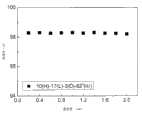
图10参照包括透镜体12的边缘厚度“T”的示例性实施例示出透射率。透镜碗的高度“H”为10mm。透镜碗的透镜长度(透镜半径)“L”为17mm。透镜的中心厚度“D”为3mm。第二曲面16的曲率的典型值为82。如图10所示,光的透射率基本不取决于透镜体的翼边缘厚度“T”。FIG. 10 illustrates the transmittance with reference to an exemplary embodiment including an edge thickness “T” of the
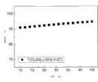
图11相对于包括第二曲面的曲率的示例性实施例示出光透射率。透镜碗的高度“H”为5mm。透镜碗的透镜长度(透镜半径)“L”为20mm。透镜的中心厚度“D”为7mm。透镜的边缘厚度“T”为0.2mm。FIG. 11 illustrates light transmission relative to an exemplary embodiment including a curvature of the second curved surface. The height "H" of the lens bowl is 5 mm. The lens length (lens radius) "L" of the lens bowl was 20 mm. The center thickness "D" of the lens is 7 mm. The edge thickness "T" of the lens is 0.2 mm.
曲率的典型值(度)越大,透射的光越多。第二曲面16的典型曲率值越大,可形成越深的散射突出13(“D”越大),从而越深的散射突出13允许越多的光被透射。The larger the typical value (degrees) of curvature, the more light is transmitted. The larger the typical curvature value of the second
图12示出图11的透镜的光分布。在图12中的(a)、(b)、(c)、(d)、(e)和(f)中的典型曲率分别包括70、76、82、88、94和100。FIG. 12 shows the light distribution of the lens of FIG. 11 . Typical curvatures in (a), (b), (c), (d), (e) and (f) in FIG. 12 include 70, 76, 82, 88, 94 and 100, respectively.
典型曲率代表第二曲面16的可变曲率。典型曲率可通过由BRO(Breault研究机构)公司开发的仿真程序来确定。仿真程序的名称为ASAP(高级系统分析程序)。The typical curvature represents a variable curvature of the second
在下面的表1中示出光分布区域。The light distribution areas are shown in Table 1 below.
表1Table 1
表1示出曲率典型值越大表示光分布越广。Table 1 shows that the larger the typical value of the curvature, the wider the light distribution.
参照图13,方点表示由半球检测器测量到的光的透射率,并且所示出的数据与上述的在图11中示出的数据相同。半球检测器检测射出透镜的所有光,并包括倾斜方向传播的光。圆点表示由平面或平坦检测器(FDET)测量到的透射率,平面或平坦检测器(FDET)不能检测在深度倾斜的方向上传播的光。平面检测器检测穿过透镜顶部一定区域的光。在示例性实施例中,本实施例的用于LED的透镜不仅向前散射光而且向倾斜的方向散射光。Referring to FIG. 13 , the square dots represent the transmittance of light measured by the hemispherical detector, and the data shown are the same as those shown in FIG. 11 described above. A hemispherical detector detects all light exiting the lens, including light propagating obliquely. The dots represent the transmittance measured by a planar or flat detector (FDET), which cannot detect light propagating in a depth-oblique direction. Flat detectors detect light passing through a certain area on top of the lens. In an exemplary embodiment, the lens for LED of the present embodiment scatters light not only forward but also in oblique directions.
图13中的方点表示由半球或圆形(曲面)检测器(CDET)测量到的透射率。三角点示出方点和圆点之差,这样三角点代表在倾斜的方向上传播的光的量。由三角点表示的方点和圆点之差被表示在以CDET-FDET(%)标示的竖直轴上。The square points in Figure 13 represent the transmittance measured by a hemispherical or circular (curved) detector (CDET). The triangular dots show the difference between the square dots and the circular dots, such that the triangular dots represent the amount of light propagating in oblique directions. The difference between the square point and the circle point represented by the triangle point is represented on the vertical axis indicated by CDET-FDET(%).
也如上所述,图14示出在透镜的第一可变曲率和第二可变曲率的各点处的曲率,该透镜的典型曲率值为70。在这种情况下,散射突出13相对小,当典型曲率值小于70时,散射突出13不能形成在第二曲面16的中心区域。As also mentioned above, FIG. 14 shows the curvature at various points of the first variable curvature and the second variable curvature of the lens, which has a typical curvature value of 70. In this case, the scattering
也如上所述,图15示出在透镜的第一可变曲率和第二可变曲率的各点处的曲率,该透镜的典型曲率值为100。As also mentioned above, FIG. 15 shows the curvature at various points of the first variable curvature and the second variable curvature of the lens, which has a typical curvature value of 100.
图16示出本发明的用于LED背光的透镜的示例性实施例的倾斜特性。在图16中的曲线表示在大约45度的极角范围内的相对均匀的光传播。FIG. 16 shows the tilt characteristics of an exemplary embodiment of the lens for LED backlight of the present invention. The curves in Figure 16 represent relatively uniform light propagation over a range of polar angles of about 45 degrees.
图17示出了本发明的示例性实施例的光透射分布。透镜碗高度“H”为5mm。透镜长度(透镜半径)“L”为20mm。中心厚度“D”为7mm。边缘厚度“T”为0.2mm。典型曲率值为70度。平面检测器检测离透镜10的表面40mm的光分布。图17示出中心的光强度比远离中心的区域的光强度弱,这是由散射突出13引起的。图17示出相对均匀的光分布。FIG. 17 shows the light transmission distribution of an exemplary embodiment of the present invention. The lens bowl height "H" is 5mm. The lens length (lens radius) "L" was 20 mm. The central thickness "D" is 7mm. Edge thickness "T" is 0.2mm. A typical curvature value is 70 degrees. The flat detector detects the light distribution at 40 mm from the surface of the
如图17所示,当透镜半径为20mm时,光分布半径为大约30mm。如上所述,透镜10设置在LED 344上。为了获得显示装置的均匀的光分布,有必要基于透镜10的光分布半径来设计包括在光源349中的LED 344和透镜10的密度(或数量)。例如,如果透镜10的光分布半径尺寸较大,则为了提供显示装置的均匀的光分布,包括在光源349中的LED 344和透镜10的数目(密度)可小于光分布半径较小时的LED 344和透镜10的数目。即,限定LED 344和透镜10的密度,以使由LED 344和透镜10共同分配的光在显示装置内提供均匀的光分布。As shown in FIG. 17, when the lens radius is 20mm, the light distribution radius is about 30mm.
在本发明的示例性实施例中,用于LED背光的透镜形成在LED上。透镜设置在LED上或紧密地附于LED,以防止光损失。辅助件(未示出)可插入在透镜和LED之间,以使LED紧密地附于透镜。In an exemplary embodiment of the present invention, a lens for an LED backlight is formed on the LED. A lens is placed on or closely attached to the LED to prevent light loss. An auxiliary piece (not shown) may be inserted between the lens and the LED to closely attach the LED to the lens.
多个LED安装在PCB(印刷电路板)上。PCB安装在背面上以形成背光单元。PCB可直接安装在后框架上。背光单元可包括多个安装在背面或后框架上的PCB。Multiple LEDs are mounted on a PCB (Printed Circuit Board). The PCB is mounted on the back to form a backlight unit. The PCB can be mounted directly on the rear frame. The backlight unit may include a plurality of PCBs mounted on the rear or rear frame.
本领域技术人员应该明白,在不脱离本发明的精神或范围的情况下,可对本发明作出各种修改和变形。因此,本发明意在覆盖本发明的修改和变形,只要这些修改和变形落入权利要求及其等同物的范围内。It will be apparent to those skilled in the art that various modifications and variations can be made in the present invention without departing from the spirit or scope of the inventions. Thus, it is intended that the present invention cover the modifications and variations of this invention provided they come within the scope of the claims and their equivalents.
Claims (24)
Translated fromChineseApplications Claiming Priority (3)
| Application Number | Priority Date | Filing Date | Title |
|---|---|---|---|
| KR10-2005-0018987 | 2005-03-08 | ||
| KR1020050018987 | 2005-03-08 | ||
| KR1020050018987AKR101112552B1 (en) | 2005-03-08 | 2005-03-08 | Lens for light emitting diode, light emitting diode, backlight assembly and liquid crystal display device comprising the same |
Publications (2)
| Publication Number | Publication Date |
|---|---|
| CN1831565A CN1831565A (en) | 2006-09-13 |
| CN1831565Btrue CN1831565B (en) | 2010-05-26 |
Family
ID=36579653
Family Applications (1)
| Application Number | Title | Priority Date | Filing Date |
|---|---|---|---|
| CN2006100586757AExpired - Fee RelatedCN1831565B (en) | 2005-03-08 | 2006-03-08 | Lens, backlight assembly with the lens and liquid crystal display with the assembly |
Country Status (6)
| Country | Link |
|---|---|
| US (1) | US7580198B2 (en) |
| EP (1) | EP1701389B1 (en) |
| JP (1) | JP4959208B2 (en) |
| KR (1) | KR101112552B1 (en) |
| CN (1) | CN1831565B (en) |
| TW (1) | TWI414826B (en) |
Families Citing this family (14)
| Publication number | Priority date | Publication date | Assignee | Title |
|---|---|---|---|---|
| KR101112552B1 (en) | 2005-03-08 | 2012-02-15 | 삼성전자주식회사 | Lens for light emitting diode, light emitting diode, backlight assembly and liquid crystal display device comprising the same |
| US7551243B2 (en) | 2006-11-21 | 2009-06-23 | Honeywell International Inc. | Lens for increased light distribution uniformity in an LCD backlight |
| US7837349B2 (en)* | 2007-06-15 | 2010-11-23 | Visteon Global Technologies, Inc. | Near field lens |
| DE102007046339A1 (en)* | 2007-09-27 | 2009-04-02 | Osram Opto Semiconductors Gmbh | Light source with variable emission characteristics |
| TWI357481B (en)* | 2008-12-05 | 2012-02-01 | Ind Tech Res Inst | A light source module for producing polarized ligh |
| US8449150B2 (en)* | 2009-02-03 | 2013-05-28 | Osram Sylvania Inc. | Tir lens for light emitting diodes |
| TW201031950A (en)* | 2009-02-26 | 2010-09-01 | xue-zhong Gao | Reflection component of light-emitting element |
| CN101936502A (en)* | 2009-06-30 | 2011-01-05 | 富准精密工业(深圳)有限公司 | Lens, light-emitting diode module and lighting device for its application |
| CN101963322A (en)* | 2009-07-21 | 2011-02-02 | 富准精密工业(深圳)有限公司 | Lens, lighting emitting diode module and lighting device |
| CN103133918B (en) | 2011-11-23 | 2015-11-11 | 财团法人工业技术研究院 | Surface light source and flexible surface light source |
| KR102174249B1 (en)* | 2014-01-17 | 2020-11-04 | 엘지이노텍 주식회사 | Material for controlling luminous flux, light emitting device and display device |
| WO2016054128A1 (en)* | 2014-09-30 | 2016-04-07 | Rambus Delaware Llc | Micro-optical element having curved surface and light guide and lighting assembly including same |
| CN111312068A (en)* | 2020-04-02 | 2020-06-19 | 深圳创维-Rgb电子有限公司 | Mini lamp bead, manufacturing method, backlight source and display device |
| EP4264128A4 (en)* | 2020-12-20 | 2024-11-20 | Glint Photonics, Inc. | OPTICAL CONCEPT FOR ADJUSTABLE REFLECTIVE LUMINAIRE |
Citations (2)
| Publication number | Priority date | Publication date | Assignee | Title |
|---|---|---|---|---|
| US2215900A (en)* | 1939-10-28 | 1940-09-24 | Ralph E Bitner | Catadioptrical lens |
| CN1580902A (en)* | 2003-08-05 | 2005-02-16 | 财团法人工业技术研究院 | Light source modulation device of function curve type lens grating |
Family Cites Families (21)
| Publication number | Priority date | Publication date | Assignee | Title |
|---|---|---|---|---|
| JP2952127B2 (en) | 1992-11-19 | 1999-09-20 | 日本電設工業 株式会社 | Light emitting device |
| IT1265106B1 (en) | 1993-07-23 | 1996-10-30 | Solari Udine Spa | OPTICAL SYSTEM FOR LIGHT-EMITTING DIODES |
| AU708420B2 (en) | 1996-01-17 | 1999-08-05 | Dialight Corporation | An led illuminated lamp assembly |
| JPH11163421A (en) | 1997-11-28 | 1999-06-18 | Toshiba Lighting & Technology Corp | Light source device and display device |
| US6536923B1 (en) | 1998-07-01 | 2003-03-25 | Sidler Gmbh & Co. | Optical attachment for a light-emitting diode and brake light for a motor vehicle |
| KR100572441B1 (en) | 1999-11-30 | 2006-04-18 | 오므론 가부시키가이샤 | Equipment using optics |
| JP2002025326A (en) | 2000-07-13 | 2002-01-25 | Seiko Epson Corp | Light source device, lighting device, liquid crystal device, and electronic device |
| US20020085390A1 (en) | 2000-07-14 | 2002-07-04 | Hironobu Kiyomoto | Optical device and apparatus employing the same |
| US6547423B2 (en) | 2000-12-22 | 2003-04-15 | Koninklijke Phillips Electronics N.V. | LED collimation optics with improved performance and reduced size |
| US6607286B2 (en) | 2001-05-04 | 2003-08-19 | Lumileds Lighting, U.S., Llc | Lens and lens cap with sawtooth portion for light emitting diode |
| JP2002344027A (en) | 2001-05-15 | 2002-11-29 | Stanley Electric Co Ltd | Surface mount LED |
| US6547432B2 (en)* | 2001-07-16 | 2003-04-15 | Stryker Instruments | Bone cement mixing and delivery device for injection and method thereof |
| US6665128B1 (en)* | 2002-07-23 | 2003-12-16 | Charles C. Tai | Corrective lens for copying books |
| US6896381B2 (en) | 2002-10-11 | 2005-05-24 | Light Prescriptions Innovators, Llc | Compact folded-optics illumination lens |
| KR101015289B1 (en) | 2002-11-05 | 2011-02-15 | 파나소닉 주식회사 | Light emitting diode |
| JP2004158830A (en)* | 2003-08-25 | 2004-06-03 | Matsushita Electric Ind Co Ltd | Light emitting diode |
| JP3988703B2 (en) | 2002-11-05 | 2007-10-10 | 松下電器産業株式会社 | Light emitting diode |
| JP4067387B2 (en)* | 2002-11-08 | 2008-03-26 | アルプス電気株式会社 | Light guiding material and lighting device |
| JP4504662B2 (en) | 2003-04-09 | 2010-07-14 | シチズン電子株式会社 | LED lamp |
| JP3977774B2 (en)* | 2003-06-03 | 2007-09-19 | ローム株式会社 | Optical semiconductor device |
| KR101112552B1 (en) | 2005-03-08 | 2012-02-15 | 삼성전자주식회사 | Lens for light emitting diode, light emitting diode, backlight assembly and liquid crystal display device comprising the same |
- 2005
- 2005-03-08KRKR1020050018987Apatent/KR101112552B1/ennot_activeExpired - Fee Related
- 2006
- 2006-03-03USUS11/367,843patent/US7580198B2/ennot_activeExpired - Fee Related
- 2006-03-07EPEP06004606.7Apatent/EP1701389B1/ennot_activeNot-in-force
- 2006-03-08CNCN2006100586757Apatent/CN1831565B/ennot_activeExpired - Fee Related
- 2006-03-08TWTW095107820Apatent/TWI414826B/ennot_activeIP Right Cessation
- 2006-03-08JPJP2006062283Apatent/JP4959208B2/ennot_activeExpired - Fee Related
Patent Citations (2)
| Publication number | Priority date | Publication date | Assignee | Title |
|---|---|---|---|---|
| US2215900A (en)* | 1939-10-28 | 1940-09-24 | Ralph E Bitner | Catadioptrical lens |
| CN1580902A (en)* | 2003-08-05 | 2005-02-16 | 财团法人工业技术研究院 | Light source modulation device of function curve type lens grating |
Also Published As
| Publication number | Publication date |
|---|---|
| KR101112552B1 (en) | 2012-02-15 |
| CN1831565A (en) | 2006-09-13 |
| EP1701389A1 (en) | 2006-09-13 |
| TW200639433A (en) | 2006-11-16 |
| TWI414826B (en) | 2013-11-11 |
| JP4959208B2 (en) | 2012-06-20 |
| EP1701389B1 (en) | 2016-05-25 |
| US20060203353A1 (en) | 2006-09-14 |
| KR20060097968A (en) | 2006-09-18 |
| US7580198B2 (en) | 2009-08-25 |
| JP2006253693A (en) | 2006-09-21 |
Similar Documents
| Publication | Publication Date | Title |
|---|---|---|
| CN1831565B (en) | Lens, backlight assembly with the lens and liquid crystal display with the assembly | |
| US7560745B2 (en) | LED package and backlight assembly for LCD comprising the same | |
| KR101621013B1 (en) | Display device | |
| JP5579381B2 (en) | Backlight system for liquid crystal display | |
| US7206491B2 (en) | Light guide device and backlight module using the same | |
| CN1952704B (en) | Light guide unit for point light source, backlight assembly having the light guide unit and display device having the same | |
| US7884896B2 (en) | Display apparatus and backlight assembly having a light guide plate comprising first and second light control patterns | |
| US9995461B2 (en) | Optical lens, light emitting device, and lighting device | |
| CN100510516C (en) | Light guide plate, as well as a planar lighting device and liquid crystal display apparatus using the same | |
| CN103703578B (en) | Light-emitting device, lighting device and display unit | |
| US9274265B2 (en) | Surface light source apparatus and display apparatus using same | |
| US20130088857A1 (en) | Optical assembly, backlight unit having the same, and display apparatus thereof | |
| CN103548160A (en) | Light emitting device, lighting device and display device | |
| CN101487945A (en) | Optical sheet and display device having the same | |
| US10352530B2 (en) | Lens, light emitting apparatus including the lens, and backlight unit including the apparatus | |
| CN101000387A (en) | Prism and backlight module using the prism | |
| CN107884989A (en) | Lens and the display device with the lens | |
| CN103765619B (en) | Light-emitting device and display device | |
| US7766533B2 (en) | Illumination module, and a display and general lighting apparatus using the same | |
| US20070229729A1 (en) | Liquid crystal display device | |
| KR20140060625A (en) | Light emitting device and lighting device having the same | |
| KR20120079363A (en) | Lens for light source, light source module having the same and backlight assembly having the same | |
| KR20100049339A (en) | Optical member and display device having the same | |
| CN100420050C (en) | Luminous light source and light source array thereof | |
| KR100557447B1 (en) | Diffuser Plate in Direct Backlight Assembly |
Legal Events
| Date | Code | Title | Description |
|---|---|---|---|
| C06 | Publication | ||
| PB01 | Publication | ||
| C10 | Entry into substantive examination | ||
| SE01 | Entry into force of request for substantive examination | ||
| C14 | Grant of patent or utility model | ||
| GR01 | Patent grant | ||
| ASS | Succession or assignment of patent right | Owner name:SAMSUNG DISPLAY CO., LTD. Free format text:FORMER OWNER: SAMSUNG ELECTRONICS CO., LTD. Effective date:20121219 | |
| C41 | Transfer of patent application or patent right or utility model | ||
| TR01 | Transfer of patent right | Effective date of registration:20121219 Address after:South Korea Gyeonggi Do Yongin Patentee after:Samsung Display Co., Ltd. Address before:Gyeonggi Do, South Korea Patentee before:Samsung Electronics Co., Ltd. | |
| CF01 | Termination of patent right due to non-payment of annual fee | ||
| CF01 | Termination of patent right due to non-payment of annual fee | Granted publication date:20100526 Termination date:20170308 |