CN1823320A - Improvements in touch technology - Google Patents
Improvements in touch technologyDownload PDFInfo
- Publication number
- CN1823320A CN1823320ACNA2004800200233ACN200480020023ACN1823320ACN 1823320 ACN1823320 ACN 1823320ACN A2004800200233 ACNA2004800200233 ACN A2004800200233ACN 200480020023 ACN200480020023 ACN 200480020023ACN 1823320 ACN1823320 ACN 1823320A
- Authority
- CN
- China
- Prior art keywords
- touchpad
- conductive
- medium
- conductive layer
- conductors
- Prior art date
- Legal status (The legal status is an assumption and is not a legal conclusion. Google has not performed a legal analysis and makes no representation as to the accuracy of the status listed.)
- Granted
Links
Images


Classifications
- G—PHYSICS
- G06—COMPUTING OR CALCULATING; COUNTING
- G06F—ELECTRIC DIGITAL DATA PROCESSING
- G06F3/00—Input arrangements for transferring data to be processed into a form capable of being handled by the computer; Output arrangements for transferring data from processing unit to output unit, e.g. interface arrangements
- G06F3/01—Input arrangements or combined input and output arrangements for interaction between user and computer
- G06F3/03—Arrangements for converting the position or the displacement of a member into a coded form
- G06F3/041—Digitisers, e.g. for touch screens or touch pads, characterised by the transducing means
- G06F3/044—Digitisers, e.g. for touch screens or touch pads, characterised by the transducing means by capacitive means
- G06F3/0445—Digitisers, e.g. for touch screens or touch pads, characterised by the transducing means by capacitive means using two or more layers of sensing electrodes, e.g. using two layers of electrodes separated by a dielectric layer
- G—PHYSICS
- G06—COMPUTING OR CALCULATING; COUNTING
- G06F—ELECTRIC DIGITAL DATA PROCESSING
- G06F3/00—Input arrangements for transferring data to be processed into a form capable of being handled by the computer; Output arrangements for transferring data from processing unit to output unit, e.g. interface arrangements
- G06F3/01—Input arrangements or combined input and output arrangements for interaction between user and computer
- G06F3/03—Arrangements for converting the position or the displacement of a member into a coded form
- G06F3/041—Digitisers, e.g. for touch screens or touch pads, characterised by the transducing means
- G06F3/044—Digitisers, e.g. for touch screens or touch pads, characterised by the transducing means by capacitive means
- G06F3/0443—Digitisers, e.g. for touch screens or touch pads, characterised by the transducing means by capacitive means using a single layer of sensing electrodes
- G—PHYSICS
- G06—COMPUTING OR CALCULATING; COUNTING
- G06F—ELECTRIC DIGITAL DATA PROCESSING
- G06F3/00—Input arrangements for transferring data to be processed into a form capable of being handled by the computer; Output arrangements for transferring data from processing unit to output unit, e.g. interface arrangements
- G06F3/01—Input arrangements or combined input and output arrangements for interaction between user and computer
- G06F3/03—Arrangements for converting the position or the displacement of a member into a coded form
- G06F3/041—Digitisers, e.g. for touch screens or touch pads, characterised by the transducing means
- G06F3/044—Digitisers, e.g. for touch screens or touch pads, characterised by the transducing means by capacitive means
- G06F3/0446—Digitisers, e.g. for touch screens or touch pads, characterised by the transducing means by capacitive means using a grid-like structure of electrodes in at least two directions, e.g. using row and column electrodes
- G—PHYSICS
- G06—COMPUTING OR CALCULATING; COUNTING
- G06F—ELECTRIC DIGITAL DATA PROCESSING
- G06F3/00—Input arrangements for transferring data to be processed into a form capable of being handled by the computer; Output arrangements for transferring data from processing unit to output unit, e.g. interface arrangements
- G06F3/01—Input arrangements or combined input and output arrangements for interaction between user and computer
- G06F3/03—Arrangements for converting the position or the displacement of a member into a coded form
- G06F3/041—Digitisers, e.g. for touch screens or touch pads, characterised by the transducing means
- G06F3/047—Digitisers, e.g. for touch screens or touch pads, characterised by the transducing means using sets of wires, e.g. crossed wires
- G—PHYSICS
- G06—COMPUTING OR CALCULATING; COUNTING
- G06K—GRAPHICAL DATA READING; PRESENTATION OF DATA; RECORD CARRIERS; HANDLING RECORD CARRIERS
- G06K11/00—Methods or arrangements for graph-reading or for converting the pattern of mechanical parameters, e.g. force or presence, into electrical signal
- H—ELECTRICITY
- H03—ELECTRONIC CIRCUITRY
- H03K—PULSE TECHNIQUE
- H03K17/00—Electronic switching or gating, i.e. not by contact-making and –breaking
- H03K17/94—Electronic switching or gating, i.e. not by contact-making and –breaking characterised by the way in which the control signals are generated
- H03K17/96—Touch switches
- H03K17/962—Capacitive touch switches
Landscapes
- Engineering & Computer Science (AREA)
- Theoretical Computer Science (AREA)
- General Engineering & Computer Science (AREA)
- Physics & Mathematics (AREA)
- General Physics & Mathematics (AREA)
- Human Computer Interaction (AREA)
- Artificial Intelligence (AREA)
- Computer Hardware Design (AREA)
- Computer Vision & Pattern Recognition (AREA)
- Position Input By Displaying (AREA)
- Switches That Are Operated By Magnetic Or Electric Fields (AREA)
Abstract
Description
Translated fromChinese技术领域technical field
本发明涉及触摸探测、邻近探测器和触摸感应表面和装置。The present invention relates to touch detection, proximity detectors and touch sensitive surfaces and devices.
背景技术Background technique
存在许多能够探测物体触摸或靠近的装置的公知实例。有些基于使用具有两组固定为相对关系的导体的膜片开关,其需要在两个导体元件的交叉处施加压力以形成电连接。这些装置的缺点是表面必须实际上被接触且使用者的手指的位置必须与导电元件交叉点一致。另外,膜片开关包括易受磨损的移动部件,因此形不成耐用的感应装置。There are many known examples of devices capable of detecting the touch or proximity of objects. Some are based on the use of a membrane switch having two sets of conductors fixed in opposing relationship, which require pressure to be applied at the intersection of the two conductor elements to form an electrical connection. The disadvantage of these devices is that the surface must actually be touched and the position of the user's finger must coincide with the intersection of the conductive elements. Additionally, membrane switches include moving parts that are subject to wear and thus do not form a durable sensing device.
可替换的感应装置使用邻近感应导体的阵列且依赖导体的电容的改变来探测与支撑导体的感应层接触或紧密邻近导体的手指的准确位置。在授予Binstead的US 6137427中描述了如此的感应装置,并在图1中显示了该装置,其中,水平和垂直的感应导体2的阵列彼此电隔离,且设置为格子结构且通过电绝缘膜片3支撑。膜片3和导体2的阵列形成触摸垫(touchpad)的感应层,如图2所示,图2为图1的装置的沿线A-B的侧横截面视图。当手指1或相似的物体触摸或接近感应层的表面时,手指引发感应层中导体2或导体组的电容的改变。使用适当的扫描设备来依次扫描每个导体2,可以测量导体2的电容的改变,且因此可以探测手指1的触摸或邻近。通过在多于一个导体2上探测电容的改变,通过在导体位置之间内插,从而可以判定手指1的触摸或邻近的准确位置。因此,电容装置能够探测感应导体2之间的手指1的位置,因此与前述的膜片开关装置不同,该电容装置不限于在导体的交叉点处探测。Alternative sensing means use an array of adjacent sensing conductors and rely on changes in the capacitance of the conductors to detect the exact position of a finger in contact with a sensing layer supporting the conductor or in close proximity to the conductor. Such an inductive arrangement is described in US 6137427 to Binstead and is shown in Figure 1, wherein the arrays of horizontal and vertical
但是,常规电容装置的缺点是当感应导体2分开较宽时将产生困难,因为导体之间的手指1的触摸或紧密邻近一般仅产生有限的用于内插处理的数据值,由此导致计算手指的准确位置的误差。However, a disadvantage of conventional capacitive devices is that difficulties arise when the
而且,常规的电容装置经受每当手掌放在该装置正上方时产生的进一步的问题,因为手掌诱发了可以错误地被鉴别为触摸动作的强信号。因为当使用者决定他们的下一个真实触摸动作时必须持续注意他们的手相对于装置的位置,所以这可能是特别不利的。Also, conventional capacitive devices suffer from further problems whenever a palm is placed directly over the device, since the palm induces a strong signal that can be falsely identified as a touch action. This may be particularly disadvantageous since the user must constantly pay attention to the position of their hand relative to the device when deciding on their next real touch action.
可以理解贯穿本说明书,对于“手指”的指代旨在包括任何能够被用于局部改变电容到通过电容感应来使探测成为可能的程度的物体。另外,任何对于“触摸”或“触摸动作”的指代旨在均包括表面的物理接触和将手指紧靠表面。It will be appreciated that throughout this specification, reference to a "finger" is intended to include any object that can be used to locally alter capacitance to the extent that detection is possible by capacitive sensing. Additionally, any reference to "touch" or "touching action" is intended to include both physical contact of a surface and pressing a finger against a surface.
发明内容Contents of the invention
本发明的一目的是至少解决一些或所有的以上问题。It is an object of the present invention to address at least some or all of the above problems.
本发明涉及触摸探测系统的构造,该系统包括改变系统的紧邻电容环境的装置。该装置可以被用于使得通过高水平的电容耦合来传播电容的变化,或用于允许该变化直接通过导电性来传播。或者,该装置可以被用于支持这些电效应。The present invention relates to the construction of a touch detection system including means for changing the immediate capacitive environment of the system. The device can be used to allow a change in capacitance to propagate through a high level of capacitive coupling, or to allow the change to propagate directly through conductivity. Alternatively, the device can be used to support these electrical effects.
本发明的一方面是提供一种方法,其改变电容触摸探测系统的导体的第一和第二系列的子组的紧邻电容环境(immediate capacitive environment),来改善系统的触摸探测的精确度和速度。One aspect of the present invention is to provide a method for changing the immediate capacitive environment of first and second series of subgroups of conductors of a capacitive touch detection system to improve the accuracy and speed of touch detection of the system .
本发明的另一方面是提供一种电阻环境的混合来控制在邻近探测(proximity detection)系统中的触摸探测的模式。Another aspect of the present invention is to provide a mixture of resistive environments to control the mode of touch detection in a proximity detection system.
本发明的另一方面是提供一种导电和/或电容耦合介质来物理地扭曲邻近探测系统的探测环境。Another aspect of the present invention is to provide a conductive and/or capacitive coupling medium to physically distort the detection environment of the proximity detection system.
根据本发明的另一方面,提供有一种触摸垫设备,包括:According to another aspect of the present invention, there is provided a touchpad device, comprising:
支撑介质,支撑多个分开的导体,其中在导体之间没有电接触,每个导体对于手指的邻近敏感以改变所述导体的电容来探测靠近所述导体的所述手指的存在,触摸垫还包括一种用来将导体之间的电场集中向支撑介质的平面的装置。a supporting medium, supporting a plurality of separate conductors, wherein there is no electrical contact between the conductors, each conductor is sensitive to the proximity of a finger to change the capacitance of said conductor to detect the presence of said finger proximate to said conductor, and the touch pad also A means is included for concentrating the electric field between the conductors towards the plane of the supporting medium.
根据本发明的另一方面,提供有一种触摸垫系统,其包括根据本发明的第一方面的触摸垫,包括:According to another aspect of the present invention, there is provided a touchpad system comprising a touchpad according to the first aspect of the present invention, comprising:
触摸感应和唤醒(wake up)电路;以及touch sensing and wake up circuitry; and
位置感应电路,其通常处于休眠且周期性地被唤醒来测量触摸垫的状态,其中,在响应触摸时,触摸感应电路唤醒位置感应电路,然后位置感应电路扫描表面来决定触摸位置。A position sensing circuit, which is usually dormant and wakes up periodically to measure the state of the touch pad, where in response to a touch, the touch sensing circuit wakes up the position sensing circuit, which then scans the surface to determine the touch location.
附图说明Description of drawings
现将通过实例并参考附图来描述本发明的实施例,在附图中:Embodiments of the invention will now be described by way of example with reference to the accompanying drawings, in which:
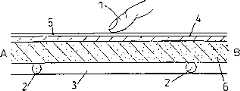
图1显示了触摸垫的感应导体设置的俯视图。Figure 1 shows a top view of the sensing conductor arrangement of the touchpad.
图2显示了常规触摸垫的、在通过图1的触摸垫的布局图的线A-B上的侧横截面图。FIG. 2 shows a side cross-sectional view of a conventional touchpad on line A-B through the layout diagram of the touchpad of FIG. 1 .
图3到11显示了本发明的触摸垫的可替换实施例的、在通过图1的触摸垫布局的线A-B上的侧横截面图。3 to 11 show side cross-sectional views of alternative embodiments of the touchpad of the present invention on line A-B through the touchpad layout of FIG. 1 .
图12显示了根据本发明在电介质的表面上电隔离导电区的设置的俯视图。Figure 12 shows a top view of an arrangement of electrically isolated conductive regions on the surface of a dielectric according to the invention.
图13显示了图12的设置沿由A-B所界定的线的侧横截面图。Figure 13 shows a side cross-sectional view of the arrangement of Figure 12 along the line bounded by A-B.
图14显示了根据本发明在电介质的表面上的电隔离导电区的另一设置的俯视图。Figure 14 shows a top view of another arrangement of electrically isolated conductive regions on the surface of a dielectric according to the invention.
图15显示了图14的设置沿A-B所界定的线的侧横截面图。Figure 15 shows a side cross-sectional view of the arrangement of Figure 14 along the line defined by A-B.
图16显示了根据本发明在电介质的第一和第二表面上的电隔离导电区的另一设置的俯视图。Figure 16 shows a top view of another arrangement of electrically isolated conductive regions on first and second surfaces of a dielectric according to the invention.
图17显示了图16的设置沿A-B所界定的线的侧横截面图。Figure 17 shows a side cross-sectional view of the arrangement of Figure 16 along the line defined by A-B.
图18显示了与本发明的触摸垫一起使用的、通过导电桥连接的导电区的图案的俯视图。Figure 18 shows a top view of a pattern of conductive regions connected by conductive bridges for use with the touchpad of the present invention.
图19和20显示了根据本发明的实施例的触摸垫的设置的侧横截面图。19 and 20 show side cross-sectional views of arrangements of touchpads according to embodiments of the invention.
图21显示了根据本发明的实施例的触摸垫的设置的部分的侧横截面图,显示有纹理的表面。Figure 21 shows a side cross-sectional view of a portion of an arrangement of a touchpad, showing a textured surface, according to an embodiment of the present invention.
图22显示了本发明的触摸垫中接地的导电介质的示意图。Fig. 22 shows a schematic diagram of a grounded conductive medium in a touchpad of the present invention.
图23显示了与本发明的触摸垫一起使用的感应系统的示意实施例。Figure 23 shows a schematic embodiment of a sensing system for use with the touchpad of the present invention.
图24显示了根据本发明的另一实施例的触摸垫设置的侧横截面图,显示在触摸垫中的间距或间隙。Figure 24 shows a side cross-sectional view of a touchpad arrangement showing the spacing or gaps in the touchpad according to another embodiment of the present invention.
图25显示了根据本发明的一实施例的触摸垫的另一设置的透视图。Figure 25 shows a perspective view of another arrangement of a touchpad according to an embodiment of the present invention.
图26到31显示了根据本发明的实施例的其他触摸垫设置的俯视图。26 to 31 show top views of other touchpad arrangements according to embodiments of the invention.
具体实施方式Detailed ways
参考图3,显示本发明的触摸垫的一个实施例。在沿图1的触摸垫布局的线A-B的侧横截面图中示出了该触摸垫,且该触摸垫包括:感应导体2的阵列;支撑介质,例如膜片3;和装置4,用于将在感应导体2之间通过的电场向支撑膜片3的平面集中。Referring to FIG. 3, one embodiment of the touchpad of the present invention is shown. The touchpad layout of FIG. 1 is shown in a side cross-sectional view along line A-B of the touchpad, and includes: an array of
感应导体2可以为US 6137427中描述的类型,且设置为平行分开的第一和第二系列的导体(如图1所示),每个导体具有在一端或两端的适当的连接,且每个系列是正交的,但彼此不电接触。因此,导体2的第一和第二系列形成多个交叉点。导体2优选地为导电引线,其具有依赖于触摸垫的具体应用的厚度。例如,在触摸屏应用中,引线优选地基本对于肉眼是不可见的,它们的直径可以小于25微米,或更具体而言其直径可以在约10微米到约25微米之间。在其他的应用中,比如互动砌筑块(interactive mansonryblock)中,引线可以为约1cm直径的加强钢筋。引线可以由铜、金、钨、铁、碳纤维或任何其他合理的良导体制成。引线优选地被电绝缘,例如通过以釉料或塑料鞘来涂布引线。The
可替换地,在其他实施例中,第一和第二系列的导体2可以由比如银基导电墨的材料制成。如果在触摸垫被用于适当的显示系统的前面的情况下导体2为低的可见度,则可以替换使用比较宽(从约250微米到1000微米)的氧化铟锡迹线。Alternatively, in other embodiments, the
在另一可替换的实施例中,第一和第二系列的导体2也可以为印刷电路板上的铜线,或TFT矩阵中相对细的铝或铜线的形式。In another alternative embodiment, the first and second series of
可以理解导体2可以在贴附到支撑膜片3之前被预成形(具有它们的自身的结构整体性),或它们可以为沉积在用于支撑的膜片上的非自支撑导体。It will be appreciated that the
可以理解可以使用将导体2从每个其他导体以及它们的周围的介质电绝缘的任何适当的方法,包括但不限于介电(例如塑料或薄玻璃)鞘或局部的介电夹层(未显示)。It will be appreciated that any suitable method of electrically insulating the
在优选的实施例中,与相同的系列中的相邻导体的导体间的间隔相比,导体2的厚度是小的,且导体间的间隔不需对于每相邻对的导体相同。根据本发明,对于10微米直径的引线的导体间的间距例如优选在约5cm到约10cm的范围,而在常规的触摸垫设置中,等效的间距则将需为约1cm。但是,可以理解导体间的间距取决于触摸垫的具体应用,且因此该实例范围不旨在为限定性的。In a preferred embodiment, the thickness of the
在其他实施例中,第一和第二系列的导体2不需平行,且第一和第二系列的导体2也不需相互垂直。In other embodiments, the first and second series of
在本发明的所有实施例中,感应导体2对手指1的邻近敏感,手指1改变了一个或多个导体的电容环境以由此探测手指1的存在。In all embodiments of the invention, the
膜片3充当用于第一和第二系列的导体2的支撑介质,且优选地由例如适当的电介质的电绝缘材料制成。在优选的实施例中,第一和第二系列的导体2除了适当的端部连接之外则完全被限定在膜片3内,端部连接可以优选地从膜片3的一侧或更多侧突出。这些端部连接被用于将感应导体连接到适当的扫描设备。The
膜片3的优选的厚度范围取决于触摸垫的具体应用。例如,在触摸屏的应用中,在引线通常被嵌入玻璃膜片的情况下,厚度可以为约4mm到约12mm。在小键盘应用中,膜片可以为约1mm厚。如果例如膜片被嵌入互动墙的砌筑块形成部分中,膜片可以为约10cm厚。但是,可以理解膜片3的厚度可以根据触摸垫的要求(例如,敏感度和弹性)来被改变。The preferred thickness range of the
在整个本说明书中,膜片3和感应导体2的组合将被称为“感应层”。Throughout this description, the combination of
可以理解膜片3不需限于平的或平面的配置,且实际上,根据本发明,膜片3可以可替换地设置为非平面、弯曲的或有角度的配置。因此,这里对“膜片的平面”的任何指代旨在均包括支撑介质的平的和非平面的配置,由此沿膜片3的表面在特定点定义的平面的方向基本相应于该点的切线的方向。因此,膜片的平面可以是遵循膜片的形状的表面轮廓。It will be appreciated that the
再次参考图3,显示出用于将感应导体之间的电场集中向膜片3的平面的装置4邻近第一和第二系列的导体2。在优选的实施例中,装置4是导电介质,设置其来允许电容的改变直接通过介质的导电性传播。在这些实施例中,导电介质4优选地具有在100欧姆每方到10000000欧姆每方(ohms persquare)的范围的电阻率。导电介质的期望的电阻率取决于感应导体2之间的导体间间距,因为宽的间距将需要更低的电阻率介质来充分地使手指诱发的电容改变明显化,以获得手指的位置的可靠的内插(interpolation)。Referring again to FIG. 3 , means 4 for concentrating the electric field between the inductive conductors towards the plane of the
在其他的优选实施例中,导电介质4被配置为通过电容耦合来传播电容变化,其中,介质的电阻率将为至少1000兆欧姆每方。在优选的实施例中,导电介质4是导电层4的形式,其覆盖膜片3的至少一部分。导电层4可以直接或不直接覆盖膜片3且依靠膜片材料和/或感应导体的电绝缘来从感应导体2电绝缘。In other preferred embodiments, the
导电层4具有范围为约25微米到约5mm范围的优选的厚度,且在典型的触摸垫设置中优选为约1mm到约2mm厚。但是,可以理解导电层4的厚度可以根据导电层4内所需的电阻而改变,因为较薄的层与较厚的层相比具有较高的电阻。
在优选的实施例中,导电层4被直接沉积在膜片3的外表面上且在其上被支撑。可以通过任何常规技术来沉积导电层4,所述技术包括但不限于电镀、溅射涂布、绘制(painting)、喷涂和用导电墨的丝网印刷/喷墨印刷。In a preferred embodiment, the
可替换地,如果导电层4形成为分开的层,则可以使用任何适当的硬化或非硬化导电粘结剂将层4结合到膜片的外表面。Alternatively, if the
在其他的实施例中,利用集中电场的装置可以提供支撑介质的功能,其中该集中装置也作为感应导体的支撑。具体的实例可以为使用例如非导电粘结带或非导电粘结剂以被结合到集中装置的引线。In other embodiments, the function of the supporting medium may be provided by means of concentrating the electric field, wherein the concentrating means also serves as a support for the induction conductor. A specific example may be the use of eg non-conductive adhesive tape or non-conductive adhesive to be bonded to the leads of the concentrator.
在本发明的一方面,导电层4具有电阻和电容特性,其强制感应导体2的触摸感应基本与膜片3的表面轮廓对准。导电层4扭曲了由手指导致的电容场,其方式为导致触摸感应基本沿导电层的表面对准,在优选的实施例中遵循了膜片3的表面轮廓。In one aspect of the invention, the
再次参考图3,导电层4的存在用于将在感应导体2之间的电场集中向膜片3的平面,从而当手指1触摸,或非常接近导电层4时,手指引发在现存电容值以上的约0.5%到约5%的电容改变。该电容改变可作为由导电层4加强的强电容信号通过感应导体2被容易地探测。因为感应导体电场的集中朝向膜片3,所以由于导电层的存在而诱发的信号显著比没有这样的层时产生的信号要大。电容信号从触摸点迅速传播开,强度随着距触摸点距离的增加而减小。在导电层4被配置为通过层的导电性直接传播电容变化的实施例中,发现电容信号衰减速率与层的电阻相关,从而高导电(低电阻)层在层的较宽区域上传播信号,与在小得多的区域上传播信号的低导电(高电阻)层相反。如果导电层4厚度及空间的范围均匀,电容信号则将从触摸点在所有方向上均匀地散播开。Referring again to Figure 3, the presence of the
横跨导电层4的任何电阻变化对于信号散播的线性度具有影响。但是,电阻的相对小变化在信号散播中产生几乎不可探测的影响,因为工作电阻范围相对而言很大。Any change in resistance across the
但是,在某些实施例中,有利的是与其他低导电率部分相比导电层4的部分具有增加的导电率,以对于如何传播电容信号施加一些程度的控制。导电率的改变可以优选地通过以下方式获得,如改变导电层4的化学组成、在层的厚度上变化、或使用这些技术的组合。However, in some embodiments it may be advantageous for portions of the
导电层4可以包括不同导电性的部分,包括没有导电性(例如,具有如此之高的电阻以至于它们基本上电绝缘)、低导电性、中等导电性和高导电性的部分。
优选地导电层4具有小于100000000欧姆每方的电阻率,或更优选地,小于10000000欧姆每方。否则,任何诱发的电容信号可以如此被重度减弱从而在信号探测上的任何优点被显著减小。Preferably the
在优选的实施例中,导电层4可以被直接触摸,如图3的实施例所示。该设置的触摸垫的灵敏度充分高以允许使用者执行触摸动作同时戴薄手套,如果将所述装置用作需要用户具有某种形式的手保护的环境中,例如在化学实验室或手术室中,或如果期望保持所述装置没有油渍和灰尘,则戴手套可能是有利的。In a preferred embodiment, the
在其他优选的实施例中,触摸垫可以包括邻近导电层4的非导电层5。优选地,非导电层5为沉积在导电层4上的薄涂层的形式,如图6所示,其防止了使用者与导电层4的直接接触。这可以被用于保护导电层4免于损伤和/或对所述装置提供抗反射涂层。非导电层也可以是纯装饰性的,或在所述装置例如被用作小键盘的情形,该层可以被印有图标或符号,指示键的位置等。在该设置中,手指1触摸非导电层5且诱发电容的变化,该变化由导电层4传播,且由此通过下面的感应导体2被探测。In other preferred embodiments, the touchpad may include a
在其他的实施例中,导电层4可以沉积于膜片3的下侧,如图4所示,且手指1可以与膜片3与导电层4相对的一侧接触或邻近。在该设置中,通过将穿过感应导体2之间的电场集中向膜片3,导电层4仍可工作来改变感应导体2的电容环境,从而可以在膜片表面上或邻近膜片表面探测手指1的触摸动作或接近。但是,因为导电层4没有被直接触摸,所有诱发的电容信号不如在前的实施例中的强。In other embodiments, the
因为导电层4被保护免于与使用者的手指1直接接触,所以图4的实施例可能是有利的,因此在正常使用期间不易受损伤和/或磨损。The embodiment of Fig. 4 may be advantageous because the
在可替换的实施例中,可以将膜片3和导电介质4组合为单一的导电支撑和感应层4A,如图5所示。在该设置中,支撑和感应层4A优选地由具有体导电性的体掺杂介质形成,其在触摸动作的时刻产生了非常强的电容信号。优选地,体掺杂介质可以是玻璃或塑料,包括导电材料的掺杂剂。In an alternative embodiment, the
常规的透明导电塑料具有非常高的电阻,通常为1000000000欧姆每方,但是这可以通过对塑料加入小量的导电颗粒、小板或纤维来减小。这些颗粒或纤维通常是不透明的,但是可以被选择以优选地为充分小以至于不可见。颗粒可以是例如铜、金或银的金属,或可以是金属氧化物。或者,可以使用石墨或其他导电物质。如果意欲这些颗粒对于肉眼保持不可见,则颗粒通常为10微米宽或更小。纤维可以是碳纤维或纳米管。这些纤维可以是短的(最大约10mm的长度)且在整个塑料中随机取向。或者,纤维可以更长且可以被松散地织为片且然后被封入塑料中。Conventional transparent conductive plastics have very high electrical resistance, typically 1000000000 ohms per square, but this can be reduced by adding small amounts of conductive particles, platelets or fibers to the plastic. These particles or fibers are generally opaque, but can be selected to preferably be sufficiently small to not be seen. The particles may be metals such as copper, gold or silver, or may be metal oxides. Alternatively, graphite or other conductive substances can be used. If it is intended that these particles remain invisible to the naked eye, the particles are typically 10 microns wide or smaller. The fibers can be carbon fibers or nanotubes. These fibers can be short (up to about 10 mm in length) and randomly oriented throughout the plastic. Alternatively, the fibers can be longer and can be loosely woven into sheets and then enclosed in plastic.
可以理解非导电塑料也可以以相同的方式用导电材料掺杂,以生产具有体导电率或改变的电容耦合的介质。It will be appreciated that non-conductive plastics can also be doped with conductive materials in the same manner to produce media with bulk conductivity or altered capacitive coupling.
通过选择颗粒和/或纤维掺杂剂的所需的量,可以制造具有所需电阻率范围的导电塑料片,其中通过塑料的支撑基体来电气性和电容性地连接塑料内的颗粒和纤维。By selecting the desired amount of particle and/or fiber dopant, conductive plastic sheets can be fabricated with a desired resistivity range, wherein the particles and fibers within the plastic are electrically and capacitively connected by the plastic's supporting matrix.
可以使用任何常规的技术成形掺杂的塑料,比如但不限于层压、真空形成或注射成型。The doped plastic can be formed using any conventional technique, such as but not limited to lamination, vacuum forming or injection molding.
在图5所示的实施例中,感应导体2优选地被完全限制在支撑和感应层4A内。但是,因为导体2优选地被电绝缘,防止了由于层的体导电性引起的导体2的短路。In the embodiment shown in Figure 5, the
支撑和感应层4A可以被直接触摸,如图5所示,且诱发的导体2的电容改变作为电容信号被在整个层中传播。在该设置中,利用处于支撑和感应层4A内的导体2诱发了大的电容信号。可以通过预选择掺杂的介质的电阻率或内电容耦合控制电容信号的传播,因为高掺杂介质将具有本征高导电率,与弱掺杂的介质相比,高掺杂介质将在层的较大体积内来传播信号,弱掺杂的介质将在层的较小体积内来传播信号。The support and
这里,贯穿说明书,术语“邻近”的使用旨在包括其中导电介质4位于一层或更多的与感应层4分开的导电层4的设置,以及其中导电介质4是组合的支撑和感应层4A的材料组分(在支撑和感应层4A中设置感应导体2)的设置。Here, throughout the specification, use of the term "adjacent" is intended to include arrangements in which the
参考图7到11,显示了根据本发明的触摸垫的其他优选的实施例。在图7中,显示了包括介电介质6的触摸垫,其被如此设置以分离膜片3和导电层4。介电介质6由任何适当的非导电介质制成,比如但不限于塑料或玻璃,且具有与导电层的厚度相比较大的厚度。介电介质的优选的厚度范围取决于触摸垫的具体应用。例如,电子销售点(epos)机可以具有约3mm到约4mm厚度的玻璃,而ATM机可以具有约12mm的玻璃。如果触摸垫通过便携计算装置(例如,膝上计算机等)的外壳来操作,则电介质(即外壳厚度)为约1.5mm。Referring to Figures 7 to 11, other preferred embodiments of the touchpad according to the present invention are shown. In FIG. 7 , a touchpad is shown comprising a
介电介质6的优点包括对于触摸垫结构的增加的支撑和强度,和对于导电层4的提高的电容耦合。Advantages of the
在优选的实施例中,导电层4可以直接沉积在介电介质6的外表面上且由此在其上被支撑,沉积使用任何常规的技术,比如但不限于电镀、溅射涂布、绘制、喷涂和用导电墨的丝网印刷/喷墨印刷。In a preferred embodiment, the
可替换地,如果导电层4形成为单独的层,则可以使用任何适当的硬化或非硬化导电粘结剂将层4结合到介电介质的外表面。Alternatively, if the
如图7所示,使用者可以触摸由介电介质6支撑的导电层4,以由此诱发膜片3中的感应导体2的电容的变化。As shown in FIG. 7 , a user may touch the
在另一实施例中,如图8所示,图7中所示的设置可以包括薄的非导电层5以保护导电层4免受损伤和/或磨损等。In another embodiment, as shown in FIG. 8, the arrangement shown in FIG. 7 may include a thin
在一个实施例中,触摸垫可以形成部分的贴附到售货窗口的背投触摸屏,所述窗口作为非导电层5。在该实例中,售货窗口可以具有约12mm厚度的玻璃,或如果安装了双层玻璃,具有约25mm的厚度。触摸屏应优选地包括75微米绘图(drafting)膜型聚酯屏,结合到具有硬化或非硬化导电粘结剂的约25微米的玻璃的外侧。聚酯屏的顶层作为显示屏和触摸表面。In one embodiment, the touchpad may form part of a rear-projection touch screen attached to a vending window, which acts as the
在进一步的实施例中,导电层4可以优选地夹在膜片3和介电介质6之间,如图9所示。在该设置中,导电层4由介电介质6保护免受损伤,介电介质6还可以对触摸垫结构加入额外的强度和支撑。使用者可以直接触摸介电介质6以诱发一个或多个下面的感应导体2的电容的变化,该变化由夹置的导电层4的存在而被增强。In a further embodiment, the
在另一实施例中,膜片可以优选地夹在导电层4和介电介质6之间,如图10所示。In another embodiment, the diaphragm may preferably be sandwiched between the
在可替换的优选实施例中,另一导电层4’可以包括在触摸垫中,如图11所示。另一导电层4’邻近介电介质,且优选地使用常规技术被沉积到介电介质6的外表面上,介电介质6具有与最初的导电层4接触的内表面,由此将所述电介质夹在两个导电层4、4’之间。另一导电层4’的存在将介电介质6的相对侧的感应导体的电场集中向介质,因此通过所述电介质提供了非常强的电容耦合,通过感应导体2对于触摸动作作出非常迅速的反应。另一导电层4’可以优选地由与最初导电层4相同的材料形成,或可替换地由任何适当的导电材料形成。In an alternative preferred embodiment, a further conductive layer 4' may be included in the touchpad, as shown in Fig. 11 . Another conductive layer 4' is adjacent to the dielectric medium and is deposited, preferably using conventional techniques, on the outer surface of
可以理解的是涉及图3到11描述的实施例是本发明的触摸垫的优选的设置,实际上,导电层和/或介电介质的任何数量和组合可以被用于生产根据本发明的触摸垫。因此,所述层和介质的层理(stratification)不旨在限制。It will be appreciated that the embodiments described with respect to FIGS. 3 to 11 are preferred arrangements for touchpads of the present invention, and that virtually any number and combination of conductive layers and/or dielectric media may be used to produce a touch pad according to the present invention. pad. Thus, the stratification of the layers and media is not intended to be limiting.
本发明的触摸垫的一个具体用途是作为数据显示和输入的触摸屏。但是,这对于可以被用于导电介质4的材料设置了限制,因为感应层和导电层4需要是透明的,使得背景显示系统对于使用者是可见的。A specific use of the touch pad of the present invention is as a touch screen for data display and input. However, this places a limit on the materials that can be used for the
优选地,可以使用比如氧化铟锡(ITO)或氧化锑锡(ATO),其可以被沉积在根据如涉及图3到11描述的任何实施例的膜片3或电介质6的表面上。但是,这些氧化物材料的缺点在于它们通常以用于本发明的材料的电阻率范围之外的电阻率来制造。氧化物通常具有10欧姆每方的电阻率,其给予导电层4一种如此之大的导电率,从而任何诱发的电容信号横跨过宽的面积传播,由此不能准确判定触摸点的位置。Preferably, eg Indium Tin Oxide (ITO) or Antimony Tin Oxide (ATO) can be used, which can be deposited on the surface of the
为了克服该问题,通过使用常规的掩模技术,包括或ITO或ATO的导电层4可以优选地被部分地蚀刻掉或沉积为不完整的层。因此,导电层4可以优选地为不连续的。To overcome this problem, the
在优选的实施例中,可以将ITO或ATO配置为多个电隔离导电“岛”或区域7。依据哪个表面支撑导电层4,这些导电区7通过膜片3或介电介质6的外表面的区域6来分隔。依据触摸屏的具体应用,导电区7可以设置为有规则的图案,或否则可以被随机设置。但是,可以理解的是为了使本发明起作用,不需严格根据下面的感应导体2的图案设置所述区域。In a preferred embodiment, the ITO or ATO can be configured as a plurality of electrically isolated conductive "islands" or
每个导电区7用于在导电区的附近集中感应导体2的电场,由此加强由接近该区域的手指靠近所引起的电容变化。Each
如果触摸垫被用作小键盘,导电区7可以优选地如此设置以至于在相应键的位置相连。可以优选地选择导电区7的尺寸和形状以至于基本相似于键尺寸的尺寸和形状。If the touchpad is used as a keypad, the
在图12中显示了如此的设置,其中导电区7以程式化的(stylised)小键盘形式来设置,在已经被选择的导电区之间具有分隔以与导电区7自身的宽度相当,即它们被较宽地分开。In Figure 12 an arrangement is shown in which the
在该设置中,当手指1触摸导电区7之一时,由感应层通过介电介质6感测电容的变化。但是,使用如此的导电区7消除了判定触摸点的准确位置的可能性,但是却在触摸时提供了强量子化的信号,允许适当的扫描设备来容易地判定哪个导电区7被触摸和何时被触摸。该效应允许不连续的导电层4被用作坐标位置指示物。In this arrangement, when a
但是,为了获得相邻的导电区7之间的强电容耦合,应使得导电区7之间的分隔尽可能的小,而在相邻导电区7之间不发生短路。由触摸垫中所需的分辨率来决定导电区7的尺寸,且优选地为分辨率的一半。例如,如果需要5mm的分辨率,则导电区应为约3mm乘3mm(即对于正方形区),在相邻区之间具有约100微米的间距。在该设置中,相邻导电区7之间的导通是不可能的,且因此导电层4作为整体不充当导电介质本身,而是通过非常强的电容耦合来耦合所述导电区。在该设置中导电层4的电阻率作为整体将在几十亿欧姆每方的量级。在图14的优选的实施例中,导电区7被紧密设置且如图15所示,相邻的导电区7被电容耦合,由此使得任何诱发的电容信号被分散到围绕触摸点的邻近的近邻。相邻的电容耦合增加了电容信号且有助于分散信号。电容信号传播通过电介质6且在下面的感应层中的感应导体2的电容环境中诱发相应的变化。However, in order to obtain strong capacitive coupling between adjacent
通过使用如涉及图11所示的实施例所述的两个导电层4、4’可以提高该效应。在该实施例中,如图16和17所示,两层导电层都是不连续的,每个都具有多个电隔离的导电区7、7’,比如通过沉积例如ITO或ATO透明氧化物形成导电区。优选地,另一导电层由介电介质6的基本相对表面来支撑,由此将另一导电层夹在介电介质6和感应层之间。另一导电层的导电区7’由介电介质6的相对表面的区域来分隔。This effect can be increased by using two
优选地,导电层的导电区7和另一导电层的导电区7’如此配置以至于基本相连,即两层包括基本对准的相同的格图案。Preferably, the
或者,导电层的导电区7和另一导电层的导电区7’被配置以至于基本重叠且非互连,即两层包括相同的小键盘图案但具有基本平移的排列。在图16和17的实施例中显示了该设置,其中通过电介质将在介电介质6的任一侧的相邻和重叠的导电区7、7’强力地电容耦合,由此加强由触摸诱发的电容信号的强度。Alternatively, the
这里在两层导电层之间的相应的导电区7、7’的区域的映射(mapping)被称为“对正(registering)”。The mapping of the areas of the respective
可以理解虽然如图12到17所例举的优选实施例显示了包括矩形导电区7、7’的程式化的小键盘,这不意味着限制,因此任何适当的几何形状可以被用作该区域的模板,例如圆形、三角形、梯形或六边形等。It will be appreciated that although the preferred embodiment as exemplified in Figures 12 to 17 shows a stylized keypad comprising rectangular
在可替换的实施例中,通过均匀地蚀刻掉大部分的沉积的导电层的厚度以产生更薄的更具电阻性的层,从而,ITO层的电阻作为整体可以优选地从本征的低的10欧姆每方增大到需要范围的值。例如,如果蚀刻掉99%的层厚,10欧姆每方的层将变为1000欧姆每方的层。In an alternative embodiment, the resistance of the ITO layer as a whole can preferably be changed from an intrinsically low Each side of 10 ohms is increased to the required range of values. For example, a layer of 10 ohms per square becomes a layer of 1000 ohms per square if 99% of the layer thickness is etched away.
或者,部分的导电层4可以优选地被完全蚀刻掉以留下多个由剩余的ITO材料的薄桥连接的导电区,例如如图18所示。优选地,导电区7具有与导电桥8的宽度相比较大的宽度。蚀刻的导电层的电阻可以还优选地通过相对于导电区7的厚度蚀刻掉导电桥8的厚度来增加。Alternatively, portions of the
可以理解虽然以上的实施例描述了使用ITO材料,但是也可以以相似的方式使用其他具有不同程度的透明度的导电材料。It will be appreciated that while the above embodiments describe the use of ITO material, other conductive materials with varying degrees of transparency may be used in a similar manner.
参考图19和20,显示有本发明的触摸垫的两个实施例,其中将触摸垫优选地设置为非平面设置,例如曲线、穹隆或正交结构。与如在前的实施例的感应导体2之间的基本线性内插不同,非平面导体层4导致了在层4的形状或表面轮廓的基础上来执行内插。这提供了这样的优点,即本来对触摸不反应的区域,比如盒子的角部或其他尖端现在可以作为感应区域,因为该层用于将在尖端区中的感应导体2之间通过的电场集中向膜片3。在非平面触摸垫配置中,将基本对准导电层4的表面轮廓执行内插。有利地,因为横跨导电层4的表面轮廓执行该内插,所以导电层4不需在端区中与膜片3或介电介质6接触,从而小的空气间隙和间距等(如图24所示)不显著影响触摸位置的判定。Referring to Figures 19 and 20, there are shown two embodiments of the touchpad of the present invention, wherein the touchpad is preferably arranged in a non-planar arrangement, such as a curved, domed or orthogonal configuration. Unlike the substantially linear interpolation between the
使用任何常规技术,触摸垫可以被形成为复杂的2和3维形状,所述常规技术包括但不限于真空形成和注射成型。触摸垫可以是有弹性的或可变形的,且根据所使用的材料,触摸垫可以具有任何程度的所需的弹性。The touchpad may be formed into complex 2- and 3-dimensional shapes using any conventional technique, including but not limited to vacuum forming and injection molding. The touchpad can be elastic or deformable, and depending on the materials used, the touchpad can have any degree of elasticity desired.
于是,采用本发明可以产生许多不同的2D和3D触摸互动材料和产品。例如,本发明可以被用于生产具有注射成型的机壳的移动电话,其自身是触摸互动的,从而不需加入分开的小键盘和/或触摸屏。对于这些应用,导电介质4可以是不透明的,由此允许使用许多更多的导电材料,包括具有表面和/或体导电性的材料。Thus, many different 2D and 3D touch-interactive materials and products can be produced using the present invention. For example, the invention could be used to produce a mobile phone with an injection molded case that is itself touch interactive, eliminating the need to incorporate a separate keypad and/or touch screen. For these applications, the
通过分区(zoning)感应导体2且在同一注射模型中具有导电和非导电的透明和不透明的塑料,触摸敏感区和非触摸敏感区可以存在于同一的注射模型中。通过如此作法,可以使前、后、侧、顶、底和所有的边缘和角部为触摸敏感的。表面可以为触摸屏、小键盘、数字化书写板、跟踪球,或当且如需要时将功能从一个转变为另一个。By zoning the
在可替换的实施例中,导电层4可以是导电纤维、导电橡胶、导电泡沫、电解质(例如,海水)、导电液态或凝胶、或甚至为导电气体,诸如等离子体。但是,可以理解几种这些材料将需要某种形式的容纳装置,比如外部的膜片来保持它们的位置且提供对于该材料的保护。在触摸时变形或改变电阻的导电介质具有附加的优点:在施加压力时与非变形介质相比,变形导电介质诱发的电容信号更强地增加,允许更大的压力感应分辨率。这在要求施加不同的压力来操作特定的功能的触摸垫的应用中可能是有利的,例如加速按钮的应用中。但是,缺点是弹性地变形的材料通常具有减小的使用寿命。在实际中,当施加更大的压力时,手指尖端自身变形,且这可以由触摸垫探测而材料自身不需变形。In alternative embodiments, the
如果将如涉及图5所述的导电支撑和感应层4A形成为如图19所示的非平面配置,该层变形了电容探测系统且允许手指1在如果使用如US 6137247中所述的纯介电系统而不可能探测到的点被探测。如图20所示,非平面触摸垫的边缘和角部仍可用于探测触摸动作,即使感应导体2距离触摸点相对远。If the conductive support and
触摸垫的表面优选地可以是平的和/或弯曲的和/或具有表面纹理(texturisation),比如凹痕、凹槽或洞等,如图21所示。表面变形允许触摸点被重新导向,同时仍可以由感应层精确地探测。图21所示的凹痕可以从导电层4延伸开一些距离,例如约1m或更多。凹痕的尖端可以通过任何适当的导体例如电引线连接回导电层4(如图25所示)。触摸凹痕的尖端将具有与在该引线结合到层4的点触摸导电层4相同的效应。引线可以电气性或电容性地连接到导电层4。The surface of the touchpad may preferably be flat and/or curved and/or have surface texturisation, such as indentations, grooves or holes, etc., as shown in FIG. 21 . Surface deformation allows touch points to be redirected while still being accurately detected by the sensing layer. The indentations shown in Figure 21 may extend some distance away from the
在优选的实施例中,导电介质4可以为电浮置,即其没有电连接到感应导体2或任何适当的扫描设备。或者,直接通过电连接13例如引线,或者通过电阻器,导电介质可以连接到地,如图22所示,由此使得导电介质4能够执行抗静电和电磁屏蔽表面的第二功能。In a preferred embodiment, the
在EP 0185671中且特别在US 6137427中描述了与本发明的触摸垫结合使用的一种适当的扫描设备。扫描设备根据模拟转换开关的顺序依次取样第一和第二系列的感应导体2的每个导体,且在存储器中存储每个电容值。这些值与来自早期扫描的基准值比较,且与在同一扫描中来自其他导体的其他电容值比较,以探测触摸事件。触摸事件必须在阈值以上才为有效的。通过具有几个阈值,可以判定触摸的压力或手指1离开触摸垫的表面的距离。A suitable scanning device for use in combination with the touchpad of the present invention is described in EP 0185671 and in particular US 6137427. The scanning device sequentially samples each conductor of the first and second series of
如果使用电池或太阳能电池,可能没有可利用的地连接,因此导电介质4可以连接到扫描设备的0伏线,或实际上连接到正性线,因为触摸垫是浮置的。在US 6137427中描述的扫描设备依赖于现有的基准地来判定何时它被触摸。电池操作的系统没有真实的地而依赖于系统的主体作为地。如果在附近有可利用的某种形式的金属件以充当接地装置则改善了该情形。将导电介质4连接到0伏线充当金属件的替代品。如果触摸垫使用者正在触摸或紧密邻近于导电介质则其有效性被极大地改善,因为该使用者作为地基准。例如,如果移动电话的整个机壳由导电介质制成,则持有该电话的动作将作为非常有效的地。移动电话的所有的表面、边缘和角部实际上可以被形成为触摸互动的,且将被使用者的手持有的任何部件可以取消激活不作为小键盘,而是作为基准地。当手离开时,该部分可以被重新激活。US 6137427的扫描设备连续地对于环境条件调整且因此可以被改进用于移动电话应用中。If a battery or solar cell is used, there may be no ground connection available, so the
在某些优选实施例中,导电介质4可以比膜片3大且可以环绕膜片3以覆盖膜片3的相反面的至少一部分。导电介质4也可以作为基准地。In some preferred embodiments, the
在引用的文件中很好地描述了扫描机制的剩余的特征,将不在这里进一步讨论。The remaining features of the scanning mechanism are well described in the cited documents and will not be discussed further here.
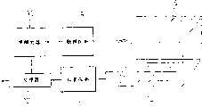
在优选的实施例中,本发明的触摸垫可以连接到感应电路,其被用于指示触摸垫被触摸的准确时间。感应电路可以诱发电压或改变导电层4上的电压。触摸垫和感应电路的组合使能够非常迅速地探测触摸,其比现有技术系统显著快。在本发明中,触摸的时间可以在约2到约3微秒内被探测,而在US 6137427的触摸探测系统中为约10毫秒。这等于在探测反应时间上约1000倍的增加,因为US 6137427的设备在判定是否发生触摸动作之前进行了触摸垫的完全扫描。但是,需要US 6137427的扫描设备来判定触摸的准确位置。In a preferred embodiment, the touchpad of the present invention may be connected to a sensing circuit, which is used to indicate the exact time the touchpad is touched. The sensing circuit can induce a voltage or change the voltage on the
优选地,感应电路包括触摸探测电路9和唤醒电路10,如图23所示,感应电路通常处于“休眠”(即,在备用模式)且周期地被唤醒来测量触摸垫的状态。触摸探测电路9将优选地连接到导电层4。在响应触摸动作时,触摸探测电路9发信号给唤醒电路10,其如果在休眠模式则唤醒感应电路,其然后通过处理器12和位置探测电路11扫描表面以判定触摸位置。在唤醒时感应电路优选地消耗约2毫安,且当通常休眠时消耗约10微安。因此,潜在可以减小功率需求100倍且提高响应时间1000倍。因此感应电路可以例如由太阳能电池或通过小电池来供电。Preferably, the sensing circuit includes a touch detection circuit 9 and a wake-
导电的接地或有源的底板(未显示)可以优选地被引入本发明的触摸垫中。在导电层和任何如此的底板之间可以需要绝缘层以防止两者之间的短路。A conductive ground or active backplane (not shown) may preferably be incorporated into the touchpad of the present invention. An insulating layer may be required between the conductive layer and any such backplane to prevent short circuits between the two.
底板必须连接到地或有源底板驱动器,且一般需要具有与本发明的触摸垫中的导电层4的优选的电阻范围相比非常低的电阻。抗静电屏蔽需要连接到大地,否则将发现其集聚电荷,减小了其作为抗静电屏蔽的功能。为了正确操作,静电屏蔽需要具有与本发明的触摸垫中的导电层4的优选的电阻范围相比非常高的电阻。The backplane must be connected to ground or an active backplane driver and generally needs to have a very low resistance compared to the preferred resistance range of the
本发明的另一应用是作为固态触摸互动片,其可以独立地在两面触摸。该片可以优选地包括夹在一对导电层之间的接地或有源的底板。Another application of the present invention is as a solid-state touch interaction sheet, which can be touched independently on both sides. The sheet may preferably comprise a grounded or active backplane sandwiched between a pair of conductive layers.
许多独立的触摸系统也可以存在于单一表面上,且可以被用于生产基本平的售货柜台,具有配置在单一平面内的多个电子销售机。为了避免相邻机器之间的任何可能的干扰,可以优选地在每个机器之间引入接大地或接地的底板。Many independent touch systems can also exist on a single surface and can be used to produce a substantially flat vending counter with multiple electronic vending machines arranged in a single plane. In order to avoid any possible interference between adjacent machines, it may be preferable to introduce a grounded or grounded chassis between each machine.
如果使用了适当的掺杂的塑料,比如涉及图5的实施例所述的塑料,导电支撑和感应层4A可以优选地附加作为扬声器的共振表面。当该表面被正在触摸时,例如当作为触摸垫操作时,该功能将被暂时中止,但将在触摸动作完成之后重新开始,由此再次产生声音。对于该应用的适当的扬声器驱动器技术可以为NXT系统。If a suitably doped plastic is used, such as that described in relation to the embodiment of Fig. 5, the conductive support and
另外,导电支撑和感应层4A可以被用作扩音器,例如使用反转的NXT系统。Alternatively, the conductive support and
在本发明的触摸垫的另一实施例中,可以包括薄柔性显示层作为触摸垫中的层。这将提供完整的触摸互动显示系统。用于显示层的适当的技术包括但不限于e墨、oled(有机发光显示器)和lep(发光聚合物)。In another embodiment of the touchpad of the present invention, a thin flexible display layer may be included as a layer in the touchpad. This will provide a complete touch-interactive display system. Suitable technologies for the display layer include but are not limited to e-ink, oled (organic light emitting display) and lep (light emitting polymer).
本发明的触摸垫的其他应用包括简单的滑动机构,其中两个感应导体通过轨形式的导电层被电容性连接(如图26所示),其中使用者向前和向后沿轨移动他的手指,模仿滑动开关的动作。轨优选地为约10cm长约1cm宽且具有约10k欧姆每方的电阻率。对于较长的轨可以减小电阻率和/或其他感应导体可以沿轨的长度设置(如图27所示)。Other applications of the touchpad of the present invention include simple sliding mechanisms in which two sensing conductors are capacitively connected through a conductive layer in the form of a rail (as shown in FIG. 26 ), where the user moves his Finger, mimicking the action of a slide switch. The rails are preferably about 10 cm long by about 1 cm wide and have a resistivity of about 10 k ohms per square. For longer rails the resistivity can be reduced and/or other inductive conductors can be placed along the length of the rail (as shown in Figure 27).
另一应用是作为计算机的简单的输入装置,比如鼠标。优选地,至少三个感应导体排列为三角配置且通过导电膜形式的导电层电容性连接(如图28所示)。在三角感应区附近的使用者的手指移动给出相对于感应导体的内插的位置,其可以被提供给计算机来控制显示屏上的光标的移动。更复杂的鼠标、跟踪球或光标控制装置可以使用其他感应导体(如图29所示),包括相关于图1所述的感应导体2的阵列(如图30所示)。Another application is as a simple input device for a computer, such as a mouse. Preferably, at least three sensing conductors are arranged in a triangular configuration and capacitively connected through a conductive layer in the form of a conductive film (as shown in FIG. 28 ). Movement of the user's finger in the vicinity of the triangular sensing area gives an interpolated position relative to the sensing conductor, which can be provided to a computer to control the movement of a cursor on the display screen. More sophisticated mouse, trackball or cursor control devices may use other sensing conductors (as shown in FIG. 29 ), including the array of
也可以将输入装置应用组合为单一的装置,使得在软件控制器的作用下可以将一个或更多的触摸感应区的功能从作为鼠标的操作改变为键盘、滑动开关、控制开关、数字化书写板等。It is also possible to combine input device applications into a single device so that the function of one or more touch-sensitive areas can be changed from operation as a mouse to a keyboard, slide switch, control switch, digitizing tablet under the action of a software controller wait.
如图31所示,例如在小键盘的应用中,触摸垫的感应导体2可以如此设置,使得每个导体相关于不同的导电区7,使得特定的区将相关的导体的电场集中向膜片的相应的部分,以提高该导体的触摸灵敏度。As shown in Figure 31, for example in keypad applications, the sensing
如果将本发明的触摸垫贴附到便携计算机装置的外壳,比如膝上计算机,触摸垫可以形成非常有效的结实的便宜的膝上鼠标。If the touchpad of the present invention is attached to the housing of a portable computer device, such as a laptop computer, the touchpad can form a very effective rugged inexpensive laptop mouse.
虽然本发明的触摸垫通过改变触摸探测系统的紧邻电容环境来理想地用于探测手指的触摸或靠近,但是可以认识到该原则可以延伸到其他类型的电容邻近感应装置和触摸探测系统。While the touchpad of the present invention is ideal for detecting the touch or proximity of a finger by altering the immediate proximity capacitive environment of the touch detection system, it will be appreciated that this principle can be extended to other types of capacitive proximity sensing devices and touch detection systems.
其他的实施例旨在落于所附权利要求的范围内。Other implementations are intended to be within the scope of the following claims.
Claims (45)
Translated fromChineseApplications Claiming Priority (2)
| Application Number | Priority Date | Filing Date | Title |
|---|---|---|---|
| GB0313808.8 | 2003-06-14 | ||
| GBGB0313808.8AGB0313808D0 (en) | 2003-06-14 | 2003-06-14 | Improvements in touch technology |
Publications (2)
| Publication Number | Publication Date |
|---|---|
| CN1823320Atrue CN1823320A (en) | 2006-08-23 |
| CN100472415C CN100472415C (en) | 2009-03-25 |
Family
ID=27636541
Family Applications (1)
| Application Number | Title | Priority Date | Filing Date |
|---|---|---|---|
| CNB2004800200233AExpired - Fee RelatedCN100472415C (en) | 2003-06-14 | 2004-06-14 | Improvements in touch technology |
Country Status (6)
| Country | Link |
|---|---|
| US (1) | US20060278444A1 (en) |
| JP (1) | JP4714144B2 (en) |
| CN (1) | CN100472415C (en) |
| DE (1) | DE112004001052T5 (en) |
| GB (2) | GB0313808D0 (en) |
| WO (1) | WO2004114105A2 (en) |
Cited By (46)
| Publication number | Priority date | Publication date | Assignee | Title |
|---|---|---|---|---|
| CN102209950A (en)* | 2008-11-11 | 2011-10-05 | 株式会社藤仓 | Position detector |
| US8105126B2 (en) | 2008-07-04 | 2012-01-31 | Tsinghua University | Method for fabricating touch panel |
| US8111245B2 (en) | 2007-12-21 | 2012-02-07 | Tsinghua University | Touch panel and display device using the same |
| US8115742B2 (en) | 2007-12-12 | 2012-02-14 | Tsinghua University | Touch panel and display device using the same |
| US8125878B2 (en) | 2007-12-27 | 2012-02-28 | Tsinghua University | Touch panel and display device using the same |
| US8199119B2 (en) | 2007-12-12 | 2012-06-12 | Beijing Funate Innovation Technology Co., Ltd. | Touch panel and display device using the same |
| US8237673B2 (en) | 2007-12-14 | 2012-08-07 | Tsinghua University | Touch panel and display device using the same |
| US8237670B2 (en) | 2007-12-12 | 2012-08-07 | Tsinghua University | Touch panel and display device using the same |
| US8237669B2 (en) | 2007-12-27 | 2012-08-07 | Tsinghua University | Touch panel and display device using the same |
| US8237668B2 (en) | 2007-12-27 | 2012-08-07 | Tsinghua University | Touch control device |
| US8237675B2 (en) | 2007-12-27 | 2012-08-07 | Tsinghua University | Touch panel and display device using the same |
| US8237671B2 (en) | 2007-12-12 | 2012-08-07 | Tsinghua University | Touch panel and display device using the same |
| US8237672B2 (en) | 2007-12-14 | 2012-08-07 | Tsinghua University | Touch panel and display device using the same |
| US8237674B2 (en) | 2007-12-12 | 2012-08-07 | Tsinghua University | Touch panel and display device using the same |
| US8243030B2 (en) | 2007-12-21 | 2012-08-14 | Tsinghua University | Touch panel and display device using the same |
| US8243029B2 (en) | 2007-12-14 | 2012-08-14 | Tsinghua University | Touch panel and display device using the same |
| US8248378B2 (en) | 2007-12-21 | 2012-08-21 | Tsinghua University | Touch panel and display device using the same |
| US8248380B2 (en) | 2007-12-14 | 2012-08-21 | Tsinghua University | Touch panel and display device using the same |
| US8248377B2 (en) | 2007-10-23 | 2012-08-21 | Tsinghua University | Touch panel |
| US8248381B2 (en) | 2007-12-12 | 2012-08-21 | Tsinghua University | Touch panel and display device using the same |
| US8248379B2 (en) | 2007-12-14 | 2012-08-21 | Tsinghua University | Touch panel, method for making the same, and display device adopting the same |
| US8253701B2 (en) | 2007-12-14 | 2012-08-28 | Tsinghua University | Touch panel, method for making the same, and display device adopting the same |
| US8253700B2 (en) | 2007-12-14 | 2012-08-28 | Tsinghua University | Touch panel and display device using the same |
| US8260378B2 (en) | 2008-08-22 | 2012-09-04 | Tsinghua University | Mobile phone |
| CN102696007A (en)* | 2010-01-05 | 2012-09-26 | 斯坦图姆公司 | Multi-contact, tactile sensor with a high electrical contact resistance |
| US8325146B2 (en) | 2007-12-21 | 2012-12-04 | Tsinghua University | Touch panel and display device using the same |
| US8325145B2 (en) | 2007-12-27 | 2012-12-04 | Tsinghua University | Touch panel and display device using the same |
| US8325585B2 (en) | 2007-12-12 | 2012-12-04 | Tsinghua University | Touch panel and display device using the same |
| US8346316B2 (en) | 2008-08-22 | 2013-01-01 | Tsinghua University | Personal digital assistant |
| US8363017B2 (en) | 2007-12-12 | 2013-01-29 | Beijing Funate Innovation Technology Co., Ltd. | Touch panel and display device using the same |
| US8390580B2 (en) | 2008-07-09 | 2013-03-05 | Tsinghua University | Touch panel, liquid crystal display screen using the same, and methods for making the touch panel and the liquid crystal display screen |
| US8411044B2 (en) | 2007-12-14 | 2013-04-02 | Tsinghua University | Touch panel, method for making the same, and display device adopting the same |
| US8502786B2 (en) | 2007-10-23 | 2013-08-06 | Tsinghua University | Touch panel |
| TWI408337B (en)* | 2008-10-07 | 2013-09-11 | Atlab Inc | Portable device with proximity sensor |
| US8542212B2 (en) | 2007-12-12 | 2013-09-24 | Tsinghua University | Touch panel, method for making the same, and display device adopting the same |
| US8574393B2 (en) | 2007-12-21 | 2013-11-05 | Tsinghua University | Method for making touch panel |
| US8585855B2 (en) | 2007-12-21 | 2013-11-19 | Tsinghua University | Method for making touch panel |
| CN102227703B (en)* | 2008-11-06 | 2014-01-08 | Uico公司 | Capacitive touch screen and strategic geometry isolation patterning method for making touch screen |
| CN103713742A (en)* | 2012-10-05 | 2014-04-09 | 新益先创科技股份有限公司 | Capacitive touch keyboard |
| CN102246131B (en)* | 2008-12-15 | 2014-11-05 | 索尼爱立信移动通讯有限公司 | Touch sensitive displays with coplanar capacitive touch and proximity sensor pads and related touch panels |
| US9040159B2 (en) | 2007-12-12 | 2015-05-26 | Tsinghua University | Electronic element having carbon nanotubes |
| CN104754263A (en)* | 2014-11-26 | 2015-07-01 | 李正浩 | Novel intelligent digital screen |
| US9077793B2 (en) | 2009-06-12 | 2015-07-07 | Tsinghua University | Carbon nanotube based flexible mobile phone |
| CN104897317A (en)* | 2015-06-18 | 2015-09-09 | 西安电子科技大学 | Flexible tactile sense-pressure sense sensor based on bionic structure |
| US9638731B2 (en) | 2012-10-05 | 2017-05-02 | Touchplus Information Corp. | Capacitive touch keyboard |
| CN111671393A (en)* | 2019-03-11 | 2020-09-18 | 郑庆生 | High-precision sensor and application thereof in force-measuring insoles |
Families Citing this family (157)
| Publication number | Priority date | Publication date | Assignee | Title |
|---|---|---|---|---|
| US7663607B2 (en) | 2004-05-06 | 2010-02-16 | Apple Inc. | Multipoint touchscreen |
| US6723299B1 (en) | 2001-05-17 | 2004-04-20 | Zyvex Corporation | System and method for manipulating nanotubes |
| US20040034177A1 (en) | 2002-05-02 | 2004-02-19 | Jian Chen | Polymer and method for using the polymer for solubilizing nanotubes |
| US6905667B1 (en) | 2002-05-02 | 2005-06-14 | Zyvex Corporation | Polymer and method for using the polymer for noncovalently functionalizing nanotubes |
| GB2421506B (en) | 2003-05-22 | 2008-07-09 | Zyvex Corp | Nanocomposites and methods thereto |
| US7296576B2 (en) | 2004-08-18 | 2007-11-20 | Zyvex Performance Materials, Llc | Polymers for enhanced solubility of nanomaterials, compositions and methods therefor |
| JP2006092814A (en)* | 2004-09-22 | 2006-04-06 | Alps Electric Co Ltd | Operation device |
| DE202005001032U1 (en)* | 2005-01-22 | 2005-05-12 | Wessling, Herbert | Gaming or gambling machine, has an operating unit in the form of a dielectric operating plate that has operating fields and matching capacitive sensors on its reverse side |
| US8049731B2 (en)* | 2005-07-29 | 2011-11-01 | Interlink Electronics, Inc. | System and method for implementing a control function via a sensor having a touch sensitive control input surface |
| DE102005041114A1 (en)* | 2005-08-30 | 2007-03-01 | BSH Bosch und Siemens Hausgeräte GmbH | Capacitive control strip for use in household appliance e.g. hob, has transverse strips that are galvanically isolated from one another, where strips overlap sensor surface in its extension transverse to strip |
| US9335855B2 (en) | 2006-04-14 | 2016-05-10 | Ritdisplay Corporation | Top-emitting OLED display having transparent touch panel |
| CN100530065C (en)* | 2006-04-20 | 2009-08-19 | 铼宝科技股份有限公司 | Transparent touch panel structure |
| CN103064569B (en)* | 2006-04-20 | 2016-08-10 | 铼宝科技股份有限公司 | Transparent touch screen with upward-emitting organic light-emitting diodes |
| US8121283B2 (en)* | 2006-05-18 | 2012-02-21 | Cypress Semiconductor Corporation | Tapered capacitive sensing structure |
| CN102981678B (en) | 2006-06-09 | 2015-07-22 | 苹果公司 | Touch screen liquid crystal display |
| US8259078B2 (en) | 2006-06-09 | 2012-09-04 | Apple Inc. | Touch screen liquid crystal display |
| CN104965621B (en) | 2006-06-09 | 2018-06-12 | 苹果公司 | Touch screen LCD and its operating method |
| JP5028552B2 (en)* | 2006-06-19 | 2012-09-19 | 株式会社Nc3 | Object detection device for detecting an object using electromagnetic induction |
| US8471822B2 (en)* | 2006-09-06 | 2013-06-25 | Apple Inc. | Dual-sided track pad |
| WO2008037275A1 (en)* | 2006-09-27 | 2008-04-03 | Nokia Corporation | Tactile touch screen |
| US8284165B2 (en) | 2006-10-13 | 2012-10-09 | Sony Corporation | Information display apparatus with proximity detection performance and information display method using the same |
| US8125456B2 (en)* | 2007-01-03 | 2012-02-28 | Apple Inc. | Multi-touch auto scanning |
| US8493330B2 (en) | 2007-01-03 | 2013-07-23 | Apple Inc. | Individual channel phase delay scheme |
| US8094128B2 (en)* | 2007-01-03 | 2012-01-10 | Apple Inc. | Channel scan logic |
| US9710095B2 (en) | 2007-01-05 | 2017-07-18 | Apple Inc. | Touch screen stack-ups |
| US8970503B2 (en) | 2007-01-05 | 2015-03-03 | Apple Inc. | Gestures for devices having one or more touch sensitive surfaces |
| US8144129B2 (en) | 2007-01-05 | 2012-03-27 | Apple Inc. | Flexible touch sensing circuits |
| US20080185193A1 (en)* | 2007-01-30 | 2008-08-07 | Jao-Ching Lin | Touch pad structure |
| US20080283310A1 (en)* | 2007-04-11 | 2008-11-20 | Moore J Douglas | System for using a ground electrode to amplify signals on a capacitance sensitive touchpad |
| GB2451267A (en)* | 2007-07-26 | 2009-01-28 | Harald Philipp | Capacitive position sensor |
| US8633915B2 (en) | 2007-10-04 | 2014-01-21 | Apple Inc. | Single-layer touch-sensitive display |
| CN101620454A (en)* | 2008-07-04 | 2010-01-06 | 清华大学 | Potable computer |
| EP2053495A3 (en) | 2007-10-23 | 2011-04-27 | Tsinghua University | Touch panel, method for making the same, and display device adopting the same |
| CN101676832B (en)* | 2008-09-19 | 2012-03-28 | 清华大学 | Desktop PC |
| DE102007052008A1 (en) | 2007-10-26 | 2009-04-30 | Andreas Steinhauser | Single- or multitouch-capable touchscreen or touchpad consisting of an array of pressure sensors and production of such sensors |
| EP2071438A3 (en) | 2007-12-14 | 2011-04-27 | Tsing Hua University | Touch panel and display device using the same |
| TWI500194B (en)* | 2007-12-21 | 2015-09-11 | Hon Hai Prec Ind Co Ltd | Touch screen, method for preparing touch screen, and display device using the same |
| US9720501B2 (en) | 2008-01-04 | 2017-08-01 | Tactus Technology, Inc. | Dynamic tactile interface |
| US9052790B2 (en) | 2008-01-04 | 2015-06-09 | Tactus Technology, Inc. | User interface and methods |
| US9128525B2 (en) | 2008-01-04 | 2015-09-08 | Tactus Technology, Inc. | Dynamic tactile interface |
| US9588683B2 (en) | 2008-01-04 | 2017-03-07 | Tactus Technology, Inc. | Dynamic tactile interface |
| US9612659B2 (en) | 2008-01-04 | 2017-04-04 | Tactus Technology, Inc. | User interface system |
| US9557915B2 (en) | 2008-01-04 | 2017-01-31 | Tactus Technology, Inc. | Dynamic tactile interface |
| US20090174676A1 (en) | 2008-01-04 | 2009-07-09 | Apple Inc. | Motion component dominance factors for motion locking of touch sensor data |
| US8947383B2 (en) | 2008-01-04 | 2015-02-03 | Tactus Technology, Inc. | User interface system and method |
| US20160187981A1 (en) | 2008-01-04 | 2016-06-30 | Tactus Technology, Inc. | Manual fluid actuator |
| US8704790B2 (en) | 2010-10-20 | 2014-04-22 | Tactus Technology, Inc. | User interface system |
| US8553005B2 (en) | 2008-01-04 | 2013-10-08 | Tactus Technology, Inc. | User interface system |
| US9063627B2 (en) | 2008-01-04 | 2015-06-23 | Tactus Technology, Inc. | User interface and methods |
| US8922510B2 (en) | 2008-01-04 | 2014-12-30 | Tactus Technology, Inc. | User interface system |
| US8570295B2 (en) | 2008-01-04 | 2013-10-29 | Tactus Technology, Inc. | User interface system |
| US9274612B2 (en) | 2008-01-04 | 2016-03-01 | Tactus Technology, Inc. | User interface system |
| US8547339B2 (en) | 2008-01-04 | 2013-10-01 | Tactus Technology, Inc. | System and methods for raised touch screens |
| US9552065B2 (en) | 2008-01-04 | 2017-01-24 | Tactus Technology, Inc. | Dynamic tactile interface |
| US8179375B2 (en)* | 2008-01-04 | 2012-05-15 | Tactus Technology | User interface system and method |
| US8154527B2 (en) | 2008-01-04 | 2012-04-10 | Tactus Technology | User interface system |
| US8456438B2 (en) | 2008-01-04 | 2013-06-04 | Tactus Technology, Inc. | User interface system |
| US9298261B2 (en) | 2008-01-04 | 2016-03-29 | Tactus Technology, Inc. | Method for actuating a tactile interface layer |
| US8243038B2 (en)* | 2009-07-03 | 2012-08-14 | Tactus Technologies | Method for adjusting the user interface of a device |
| US9423875B2 (en) | 2008-01-04 | 2016-08-23 | Tactus Technology, Inc. | Dynamic tactile interface with exhibiting optical dispersion characteristics |
| US8179377B2 (en)* | 2009-01-05 | 2012-05-15 | Tactus Technology | User interface system |
| US9430074B2 (en) | 2008-01-04 | 2016-08-30 | Tactus Technology, Inc. | Dynamic tactile interface |
| EP2085861A1 (en)* | 2008-01-29 | 2009-08-05 | Research In Motion Limited | Electronic device and touch screen display |
| US10969917B2 (en)* | 2008-01-30 | 2021-04-06 | Apple Inc. | Auto scanning for multiple frequency stimulation multi-touch sensor panels |
| EP2863295B1 (en) | 2008-02-28 | 2019-10-16 | 3M Innovative Properties Company | Touch screen sensor having varying sheet resistance |
| US20090231282A1 (en)* | 2008-03-14 | 2009-09-17 | Steven Fyke | Character selection on a device using offset contact-zone |
| JP5133791B2 (en)* | 2008-06-19 | 2013-01-30 | 株式会社ジャパンディスプレイイースト | Display device with touch panel |
| DE102008030464A1 (en)* | 2008-06-26 | 2009-12-31 | Wmf Württembergische Metallwarenfabrik Ag | Switching device for e.g. switching off, e.g. TV set, has sensor device i.e. capacitive on-off switch, for detaching electrical device from network, and photovoltaic and/or solar cell supplying sensor device with electrical energy |
| TWI403928B (en)* | 2008-07-11 | 2013-08-01 | Hon Hai Prec Ind Co Ltd | Touch screen preparation method |
| JP5123774B2 (en)* | 2008-07-25 | 2013-01-23 | 株式会社ジャパンディスプレイイースト | Input device and display device including the same |
| JP2010108501A (en)* | 2008-10-30 | 2010-05-13 | Samsung Electronics Co Ltd | Touch screen controller having increased sensing sensitivity, and display driving circuit and display device and system having the touch screen controller |
| WO2010078596A1 (en)* | 2009-01-05 | 2010-07-08 | Tactus Technology, Inc. | User interface system |
| US9588684B2 (en) | 2009-01-05 | 2017-03-07 | Tactus Technology, Inc. | Tactile interface for a computing device |
| US20100182271A1 (en)* | 2009-01-21 | 2010-07-22 | James Frederick Krier | Method for achieving a decorative backlit sensing panel with complex curvature |
| US8922521B2 (en) | 2009-02-02 | 2014-12-30 | Apple Inc. | Switching circuitry for touch sensitive display |
| US9261997B2 (en) | 2009-02-02 | 2016-02-16 | Apple Inc. | Touch regions in diamond configuration |
| US9317140B2 (en)* | 2009-03-30 | 2016-04-19 | Microsoft Technology Licensing, Llc | Method of making a multi-touch input device for detecting touch on a curved surface |
| US8982051B2 (en)* | 2009-03-30 | 2015-03-17 | Microsoft Technology Licensing, Llc | Detecting touch on a surface |
| TWI419034B (en)* | 2009-04-03 | 2013-12-11 | Novatek Microelectronics Corp | A control method of detecting a touch event for a touch panel and related device |
| US8593410B2 (en) | 2009-04-10 | 2013-11-26 | Apple Inc. | Touch sensor panel design |
| JP5429636B2 (en)* | 2009-04-10 | 2014-02-26 | Nltテクノロジー株式会社 | Touch sensor device and electronic apparatus equipped with the same |
| US8957874B2 (en) | 2009-06-29 | 2015-02-17 | Apple Inc. | Touch sensor panel design |
| WO2011003113A1 (en) | 2009-07-03 | 2011-01-06 | Tactus Technology | User interface enhancement system |
| TWM383782U (en)* | 2009-07-14 | 2010-07-01 | Ultrachip Inc | Resistance touch panel |
| US8432322B2 (en) | 2009-07-17 | 2013-04-30 | Apple Inc. | Electronic devices with capacitive proximity sensors for proximity-based radio-frequency power control |
| GB0913734D0 (en) | 2009-08-06 | 2009-09-16 | Binstead Ronald P | Masked touch sensors |
| JP5548270B2 (en) | 2009-08-21 | 2014-07-16 | アップル インコーポレイテッド | Capacitive sensing method and apparatus |
| US20110134050A1 (en)* | 2009-12-07 | 2011-06-09 | Harley Jonah A | Fabrication of touch sensor panel using laser ablation |
| CN102782617B (en)* | 2009-12-21 | 2015-10-07 | 泰克图斯科技公司 | User interface system |
| WO2011087816A1 (en)* | 2009-12-21 | 2011-07-21 | Tactus Technology | User interface system |
| US9298262B2 (en) | 2010-01-05 | 2016-03-29 | Tactus Technology, Inc. | Dynamic tactile interface |
| KR101309864B1 (en)* | 2010-02-02 | 2013-09-16 | 엘지디스플레이 주식회사 | Mask Assembly |
| US8619035B2 (en) | 2010-02-10 | 2013-12-31 | Tactus Technology, Inc. | Method for assisting user input to a device |
| CN102741791B (en)* | 2010-02-17 | 2016-01-13 | 三菱电机株式会社 | Touch panel device |
| WO2011112984A1 (en) | 2010-03-11 | 2011-09-15 | Tactus Technology | User interface system |
| WO2011133605A1 (en) | 2010-04-19 | 2011-10-27 | Tactus Technology | Method of actuating a tactile interface layer |
| WO2011133604A1 (en) | 2010-04-19 | 2011-10-27 | Tactus Technology | User interface system |
| DE202010007241U1 (en)* | 2010-05-26 | 2011-09-23 | Cooper Tools Gmbh | soldering System |
| US9652088B2 (en) | 2010-07-30 | 2017-05-16 | Apple Inc. | Fabrication of touch sensor panel using laser ablation |
| JP5740114B2 (en)* | 2010-08-19 | 2015-06-24 | 株式会社ジャパンディスプレイ | Display device |
| US20120068934A1 (en)* | 2010-09-17 | 2012-03-22 | Microsoft Corporation | Interactive keyboard with viewable display |
| US20130284578A1 (en)* | 2010-09-20 | 2013-10-31 | Printechnologics Gmbh | Information carrier and system for acquiring information |
| CN103124946B (en) | 2010-10-20 | 2016-06-29 | 泰克图斯科技公司 | User interface system and method |
| US8804056B2 (en) | 2010-12-22 | 2014-08-12 | Apple Inc. | Integrated touch screens |
| US8952860B2 (en) | 2011-03-01 | 2015-02-10 | Apple Inc. | Antenna structures with carriers and shields |
| US8692799B1 (en) | 2011-07-05 | 2014-04-08 | Cypress Semiconductor Corporation | Single layer multi-touch capacitive sensor |
| CN102360268A (en)* | 2011-09-30 | 2012-02-22 | 中兴通讯股份有限公司 | Ebook page turning method and device and mobile equipment |
| US20130155001A1 (en)* | 2011-12-19 | 2013-06-20 | Esat Yilmaz | Low-Resistance Electrodes |
| US9007333B1 (en) | 2012-02-23 | 2015-04-14 | Cypress Semiconductor Corporation | Touch sensor pattern |
| US9329723B2 (en) | 2012-04-16 | 2016-05-03 | Apple Inc. | Reconstruction of original touch image from differential touch image |
| WO2014047656A2 (en) | 2012-09-24 | 2014-03-27 | Tactus Technology, Inc. | Dynamic tactile interface and methods |
| US9405417B2 (en) | 2012-09-24 | 2016-08-02 | Tactus Technology, Inc. | Dynamic tactile interface and methods |
| US9785217B2 (en) | 2012-09-28 | 2017-10-10 | Synaptics Incorporated | System and method for low power input object detection and interaction |
| JP6012437B2 (en)* | 2012-11-29 | 2016-10-25 | シナプティクス・ジャパン合同会社 | Semiconductor device and electronic equipment |
| JP5565598B1 (en)* | 2013-02-01 | 2014-08-06 | パナソニック インテレクチュアル プロパティ コーポレーション オブ アメリカ | Electronic device, input processing method, and program |
| TW201433945A (en)* | 2013-02-26 | 2014-09-01 | Hon Hai Prec Ind Co Ltd | Electronic device and human-computer interaction method |
| US9557813B2 (en) | 2013-06-28 | 2017-01-31 | Tactus Technology, Inc. | Method for reducing perceived optical distortion |
| US9886141B2 (en) | 2013-08-16 | 2018-02-06 | Apple Inc. | Mutual and self capacitance touch measurements in touch panel |
| US10025412B2 (en) | 2013-10-16 | 2018-07-17 | Synaptics Incorporated | In-cell low power modes |
| FR3013472B1 (en) | 2013-11-19 | 2016-07-08 | Fogale Nanotech | COVERING ACCESSORY DEVICE FOR AN ELECTRONIC AND / OR COMPUTER PORTABLE APPARATUS, AND APPARATUS EQUIPPED WITH SUCH AN ACCESSORY DEVICE |
| US9379445B2 (en) | 2014-02-14 | 2016-06-28 | Apple Inc. | Electronic device with satellite navigation system slot antennas |
| US11085184B2 (en) | 2014-02-20 | 2021-08-10 | Dirtt Environmental Solutions Ltd. | Interface for mounting interchangable components |
| US9583838B2 (en) | 2014-03-20 | 2017-02-28 | Apple Inc. | Electronic device with indirectly fed slot antennas |
| US9559425B2 (en) | 2014-03-20 | 2017-01-31 | Apple Inc. | Electronic device with slot antenna and proximity sensor |
| KR101581412B1 (en) | 2014-04-01 | 2015-12-30 | (주)엔피홀딩스 | Digitizer |
| US20170024124A1 (en)* | 2014-04-14 | 2017-01-26 | Sharp Kabushiki Kaisha | Input device, and method for controlling input device |
| US9728858B2 (en) | 2014-04-24 | 2017-08-08 | Apple Inc. | Electronic devices with hybrid antennas |
| WO2015178920A1 (en) | 2014-05-22 | 2015-11-26 | Onamp Research Llc | Panel bootstrapping architectures for in-cell self-capacitance |
| US10289251B2 (en) | 2014-06-27 | 2019-05-14 | Apple Inc. | Reducing floating ground effects in pixelated self-capacitance touch screens |
| US9880655B2 (en) | 2014-09-02 | 2018-01-30 | Apple Inc. | Method of disambiguating water from a finger touch on a touch sensor panel |
| KR20160034135A (en)* | 2014-09-19 | 2016-03-29 | 삼성전자주식회사 | Device for Handling Touch Input and Method Thereof |
| WO2016048269A1 (en) | 2014-09-22 | 2016-03-31 | Onamp Research Llc | Ungrounded user signal compensation for pixelated self-capacitance touch sensor panel |
| JP6241402B2 (en)* | 2014-10-06 | 2017-12-06 | Jfeスチール株式会社 | Contact detection device, contact detection method, and wrinkle detector |
| EP3213173A4 (en) | 2014-10-27 | 2018-06-06 | Apple Inc. | Pixelated self-capacitance water rejection |
| US10795488B2 (en) | 2015-02-02 | 2020-10-06 | Apple Inc. | Flexible self-capacitance and mutual capacitance touch sensing system architecture |
| US10488992B2 (en) | 2015-03-10 | 2019-11-26 | Apple Inc. | Multi-chip touch architecture for scalability |
| WO2016149362A1 (en)* | 2015-03-16 | 2016-09-22 | Dirtt Environmental Solutions, Inc. | Glass panel reconfigurable wall panels |
| US10218052B2 (en) | 2015-05-12 | 2019-02-26 | Apple Inc. | Electronic device with tunable hybrid antennas |
| US9813059B2 (en)* | 2015-08-15 | 2017-11-07 | Ching-Hsiung Chu | Capacitive sensitive key structure |
| US10365773B2 (en) | 2015-09-30 | 2019-07-30 | Apple Inc. | Flexible scan plan using coarse mutual capacitance and fully-guarded measurements |
| US10191600B2 (en) | 2015-10-21 | 2019-01-29 | Microsoft Technology Licensing, Llc | Device with mechanical keys and capacitance measurement |
| US10908742B2 (en) | 2015-10-21 | 2021-02-02 | Microsoft Technology Licensing, Llc | Device with grooves in conductive casing |
| US10490881B2 (en) | 2016-03-10 | 2019-11-26 | Apple Inc. | Tuning circuits for hybrid electronic device antennas |
| ES2636016B1 (en)* | 2016-04-04 | 2018-06-18 | Jesús Manuel NOVO REY | Rear touch panel installed on the cover of a mobile device and procedure for the activation of functions through said panel |
| EP3322863A4 (en) | 2016-06-10 | 2019-05-01 | DIRTT Environmental Solutions, Ltd. | GLASS SUBSTRATES WITH TOUCH SCREEN TECHNOLOGY |
| CA2992856A1 (en) | 2016-06-10 | 2017-12-14 | Dirtt Environmental Solutions Inc. | Wall system with electronic device mounting assembly |
| CA3030282A1 (en) | 2016-07-08 | 2018-01-11 | Dirtt Environmental Solutions, Inc. | Low-voltage smart glass |
| AU2017208277B2 (en) | 2016-09-06 | 2018-12-20 | Apple Inc. | Back of cover touch sensors |
| US10290946B2 (en) | 2016-09-23 | 2019-05-14 | Apple Inc. | Hybrid electronic device antennas having parasitic resonating elements |
| US10642418B2 (en) | 2017-04-20 | 2020-05-05 | Apple Inc. | Finger tracking in wet environment |
| US10668627B2 (en)* | 2017-09-26 | 2020-06-02 | Toyota Research Institute, Inc. | Deformable sensors and methods for detecting pose and force against an object |
| US10747404B2 (en)* | 2017-10-24 | 2020-08-18 | Microchip Technology Incorporated | Touchscreen including tactile feedback structures and corresponding virtual user interface elements |
| US11036341B1 (en) | 2018-09-27 | 2021-06-15 | Apple Inc. | Conductive components in an insulator layer of a touch sensor stackup |
| US11157109B1 (en) | 2019-09-06 | 2021-10-26 | Apple Inc. | Touch sensing with water rejection |
| CN111245418B (en)* | 2020-01-15 | 2023-05-05 | 业成科技(成都)有限公司 | Switch module |
| US11662867B1 (en) | 2020-05-30 | 2023-05-30 | Apple Inc. | Hover detection on a touch sensor panel |
| CN113108817B (en)* | 2021-04-26 | 2025-05-13 | 远峰科技股份有限公司 | PCB capacitive sensor and smart door lock control switch |
Family Cites Families (30)
| Publication number | Priority date | Publication date | Assignee | Title |
|---|---|---|---|---|
| JPS5923410B2 (en)* | 1978-06-09 | 1984-06-01 | パナフアコム株式会社 | tatsuchi keyboard |
| US4686332A (en)* | 1986-06-26 | 1987-08-11 | International Business Machines Corporation | Combined finger touch and stylus detection system for use on the viewing surface of a visual display device |
| JPS58211241A (en)* | 1982-05-31 | 1983-12-08 | Fujitsu Ltd | Touch type coordinate detection panel |
| JPS5936550U (en)* | 1982-08-31 | 1984-03-07 | 富士通株式会社 | Finger touch coordinate detection panel |
| JPS60140419A (en)* | 1983-12-27 | 1985-07-25 | Canon Inc | panel switch |
| GB8409877D0 (en)* | 1984-04-17 | 1984-05-31 | Binstead Ronald Peter | Capacitance effect keyboard |
| JPS60192033U (en)* | 1984-05-25 | 1985-12-20 | カシオ計算機株式会社 | handwriting input device |
| US5083118A (en)* | 1990-04-16 | 1992-01-21 | Pentel Kabushiki Kaisha | Transparent coordinate input apparatus for electrostatic capacity coupling system |
| US5543588A (en)* | 1992-06-08 | 1996-08-06 | Synaptics, Incorporated | Touch pad driven handheld computing device |
| US5942733A (en)* | 1992-06-08 | 1999-08-24 | Synaptics, Inc. | Stylus input capacitive touchpad sensor |
| GB9406702D0 (en)* | 1994-04-05 | 1994-05-25 | Binstead Ronald P | Multiple input proximity detector and touchpad system |
| US5548306A (en)* | 1994-04-28 | 1996-08-20 | At&T Global Information Solutions Company | Visible and touchable touch screen shield |
| US5657053A (en)* | 1995-04-26 | 1997-08-12 | Texas Instruments Incorporated | Method for determining pen location on display apparatus using piezoelectric point elements |
| US5828773A (en)* | 1996-01-26 | 1998-10-27 | Harris Corporation | Fingerprint sensing method with finger position indication |
| JPH09212302A (en)* | 1996-01-30 | 1997-08-15 | Alps Electric Co Ltd | Coordinate input device |
| US6088471A (en)* | 1997-05-16 | 2000-07-11 | Authentec, Inc. | Fingerprint sensor including an anisotropic dielectric coating and associated methods |
| CN2366897Y (en)* | 1998-09-14 | 2000-03-01 | 深圳桑达太平洋网络系统工程有限公司 | Low power consumption and card drawing-near type testing device |
| US6297811B1 (en)* | 1999-06-02 | 2001-10-02 | Elo Touchsystems, Inc. | Projective capacitive touchscreen |
| JP2001222378A (en)* | 2000-02-10 | 2001-08-17 | Nec Saitama Ltd | Touch panel input device |
| US6847354B2 (en)* | 2000-03-23 | 2005-01-25 | The United States Of America As Represented By The Administrator Of The National Aeronautics And Space Administration | Three dimensional interactive display |
| FI117811B (en)* | 2000-05-15 | 2007-02-28 | Nokia Corp | Device and method for realizing a key |
| JP3785086B2 (en)* | 2000-11-27 | 2006-06-14 | 敏秋 石山 | Glass touch panel and manufacturing method thereof |
| TW507158B (en)* | 2001-01-05 | 2002-10-21 | Darfon Electronics Corp | Detecting device and method of mouse touch pad |
| US6822640B2 (en)* | 2001-04-10 | 2004-11-23 | Hewlett-Packard Development Company, L.P. | Illuminated touch pad |
| CN1275131C (en)* | 2001-08-22 | 2006-09-13 | 夏普株式会社 | Touch sensor, display device with touch sensor and position data generation method |
| FR2832240A1 (en)* | 2001-11-13 | 2003-05-16 | St Microelectronics Sa | Contact sensor for finger of stylus for use with a pocket computer, etc., whereby sensor has a low resolution low power operation mode for command input and a high resolution high power mode for fingerprint authentication |
| JP3880888B2 (en)* | 2002-06-18 | 2007-02-14 | Smk株式会社 | Tablet device |
| US7190354B2 (en)* | 2002-07-15 | 2007-03-13 | Fuji Photo Film Co., Ltd. | Inner type touch panel, process for producing the same and display unit |
| US6970160B2 (en)* | 2002-12-19 | 2005-11-29 | 3M Innovative Properties Company | Lattice touch-sensing system |
| JP4009953B2 (en)* | 2003-05-14 | 2007-11-21 | オムロン株式会社 | Object detection sensor |
- 2003
- 2003-06-14GBGBGB0313808.8Apatent/GB0313808D0/ennot_activeCeased
- 2004
- 2004-06-14DEDE112004001052Tpatent/DE112004001052T5/ennot_activeCeased
- 2004-06-14WOPCT/GB2004/002511patent/WO2004114105A2/enactiveApplication Filing
- 2004-06-14USUS10/560,701patent/US20060278444A1/ennot_activeAbandoned
- 2004-06-14CNCNB2004800200233Apatent/CN100472415C/ennot_activeExpired - Fee Related
- 2004-06-14GBGB0525271Apatent/GB2418259B/ennot_activeExpired - Fee Related
- 2004-06-14JPJP2006516408Apatent/JP4714144B2/ennot_activeExpired - Fee Related
Cited By (55)
| Publication number | Priority date | Publication date | Assignee | Title |
|---|---|---|---|---|
| US8502786B2 (en) | 2007-10-23 | 2013-08-06 | Tsinghua University | Touch panel |
| US8248377B2 (en) | 2007-10-23 | 2012-08-21 | Tsinghua University | Touch panel |
| US8363017B2 (en) | 2007-12-12 | 2013-01-29 | Beijing Funate Innovation Technology Co., Ltd. | Touch panel and display device using the same |
| US8237671B2 (en) | 2007-12-12 | 2012-08-07 | Tsinghua University | Touch panel and display device using the same |
| US8248381B2 (en) | 2007-12-12 | 2012-08-21 | Tsinghua University | Touch panel and display device using the same |
| US9040159B2 (en) | 2007-12-12 | 2015-05-26 | Tsinghua University | Electronic element having carbon nanotubes |
| US8199119B2 (en) | 2007-12-12 | 2012-06-12 | Beijing Funate Innovation Technology Co., Ltd. | Touch panel and display device using the same |
| US8542212B2 (en) | 2007-12-12 | 2013-09-24 | Tsinghua University | Touch panel, method for making the same, and display device adopting the same |
| US8325585B2 (en) | 2007-12-12 | 2012-12-04 | Tsinghua University | Touch panel and display device using the same |
| US8237670B2 (en) | 2007-12-12 | 2012-08-07 | Tsinghua University | Touch panel and display device using the same |
| US8237674B2 (en) | 2007-12-12 | 2012-08-07 | Tsinghua University | Touch panel and display device using the same |
| US8115742B2 (en) | 2007-12-12 | 2012-02-14 | Tsinghua University | Touch panel and display device using the same |
| US8253701B2 (en) | 2007-12-14 | 2012-08-28 | Tsinghua University | Touch panel, method for making the same, and display device adopting the same |
| US8237673B2 (en) | 2007-12-14 | 2012-08-07 | Tsinghua University | Touch panel and display device using the same |
| US8248379B2 (en) | 2007-12-14 | 2012-08-21 | Tsinghua University | Touch panel, method for making the same, and display device adopting the same |
| US8237672B2 (en) | 2007-12-14 | 2012-08-07 | Tsinghua University | Touch panel and display device using the same |
| US8253700B2 (en) | 2007-12-14 | 2012-08-28 | Tsinghua University | Touch panel and display device using the same |
| US8411044B2 (en) | 2007-12-14 | 2013-04-02 | Tsinghua University | Touch panel, method for making the same, and display device adopting the same |
| US8243029B2 (en) | 2007-12-14 | 2012-08-14 | Tsinghua University | Touch panel and display device using the same |
| US8248380B2 (en) | 2007-12-14 | 2012-08-21 | Tsinghua University | Touch panel and display device using the same |
| US8325146B2 (en) | 2007-12-21 | 2012-12-04 | Tsinghua University | Touch panel and display device using the same |
| US8243030B2 (en) | 2007-12-21 | 2012-08-14 | Tsinghua University | Touch panel and display device using the same |
| US8585855B2 (en) | 2007-12-21 | 2013-11-19 | Tsinghua University | Method for making touch panel |
| US8574393B2 (en) | 2007-12-21 | 2013-11-05 | Tsinghua University | Method for making touch panel |
| US8248378B2 (en) | 2007-12-21 | 2012-08-21 | Tsinghua University | Touch panel and display device using the same |
| US8111245B2 (en) | 2007-12-21 | 2012-02-07 | Tsinghua University | Touch panel and display device using the same |
| US8237668B2 (en) | 2007-12-27 | 2012-08-07 | Tsinghua University | Touch control device |
| US8325145B2 (en) | 2007-12-27 | 2012-12-04 | Tsinghua University | Touch panel and display device using the same |
| US8125878B2 (en) | 2007-12-27 | 2012-02-28 | Tsinghua University | Touch panel and display device using the same |
| US8237669B2 (en) | 2007-12-27 | 2012-08-07 | Tsinghua University | Touch panel and display device using the same |
| US8237675B2 (en) | 2007-12-27 | 2012-08-07 | Tsinghua University | Touch panel and display device using the same |
| US8105126B2 (en) | 2008-07-04 | 2012-01-31 | Tsinghua University | Method for fabricating touch panel |
| US8237680B2 (en) | 2008-07-04 | 2012-08-07 | Tsinghua University | Touch panel |
| US8237677B2 (en) | 2008-07-04 | 2012-08-07 | Tsinghua University | Liquid crystal display screen |
| US8199123B2 (en) | 2008-07-04 | 2012-06-12 | Tsinghua University | Method for making liquid crystal display screen |
| US8228308B2 (en) | 2008-07-04 | 2012-07-24 | Tsinghua University | Method for making liquid crystal display adopting touch panel |
| US8237679B2 (en) | 2008-07-04 | 2012-08-07 | Tsinghua University | Liquid crystal display screen |
| US8390580B2 (en) | 2008-07-09 | 2013-03-05 | Tsinghua University | Touch panel, liquid crystal display screen using the same, and methods for making the touch panel and the liquid crystal display screen |
| US8411052B2 (en) | 2008-07-09 | 2013-04-02 | Tsinghua University | Touch panel, liquid crystal display screen using the same, and methods for making the touch panel and the liquid crystal display screen |
| US8411051B2 (en) | 2008-07-09 | 2013-04-02 | Tsinghua University | Liquid crystal display screen |
| US8260378B2 (en) | 2008-08-22 | 2012-09-04 | Tsinghua University | Mobile phone |
| US8346316B2 (en) | 2008-08-22 | 2013-01-01 | Tsinghua University | Personal digital assistant |
| TWI408337B (en)* | 2008-10-07 | 2013-09-11 | Atlab Inc | Portable device with proximity sensor |
| CN102227703B (en)* | 2008-11-06 | 2014-01-08 | Uico公司 | Capacitive touch screen and strategic geometry isolation patterning method for making touch screen |
| CN102209950B (en)* | 2008-11-11 | 2014-05-07 | 株式会社藤仓 | Position detector |
| CN102209950A (en)* | 2008-11-11 | 2011-10-05 | 株式会社藤仓 | Position detector |
| CN102246131B (en)* | 2008-12-15 | 2014-11-05 | 索尼爱立信移动通讯有限公司 | Touch sensitive displays with coplanar capacitive touch and proximity sensor pads and related touch panels |
| US9077793B2 (en) | 2009-06-12 | 2015-07-07 | Tsinghua University | Carbon nanotube based flexible mobile phone |
| CN102696007A (en)* | 2010-01-05 | 2012-09-26 | 斯坦图姆公司 | Multi-contact, tactile sensor with a high electrical contact resistance |
| CN103713742A (en)* | 2012-10-05 | 2014-04-09 | 新益先创科技股份有限公司 | Capacitive touch keyboard |
| US9638731B2 (en) | 2012-10-05 | 2017-05-02 | Touchplus Information Corp. | Capacitive touch keyboard |
| CN104754263A (en)* | 2014-11-26 | 2015-07-01 | 李正浩 | Novel intelligent digital screen |
| CN104897317A (en)* | 2015-06-18 | 2015-09-09 | 西安电子科技大学 | Flexible tactile sense-pressure sense sensor based on bionic structure |
| CN104897317B (en)* | 2015-06-18 | 2018-03-06 | 西安电子科技大学 | Flexible contact pressing based on biomimetic features feels sensor |
| CN111671393A (en)* | 2019-03-11 | 2020-09-18 | 郑庆生 | High-precision sensor and application thereof in force-measuring insoles |
Also Published As
| Publication number | Publication date |
|---|---|
| CN100472415C (en) | 2009-03-25 |
| GB2418259A (en) | 2006-03-22 |
| JP2006527438A (en) | 2006-11-30 |
| GB0525271D0 (en) | 2006-01-18 |
| WO2004114105A3 (en) | 2005-09-15 |
| JP4714144B2 (en) | 2011-06-29 |
| DE112004001052T5 (en) | 2006-05-11 |
| GB2418259B (en) | 2007-08-08 |
| GB0313808D0 (en) | 2003-07-23 |
| WO2004114105A2 (en) | 2004-12-29 |
| US20060278444A1 (en) | 2006-12-14 |
Similar Documents
| Publication | Publication Date | Title |
|---|---|---|
| CN1823320A (en) | Improvements in touch technology | |
| JP5039747B2 (en) | Input device and display device including the same | |
| CN1307528C (en) | Touch panel and manufacturing method thereof, liquid crystal display device and manufacturing method thereof | |
| JP5403815B2 (en) | Input device and display device including the same | |
| CN100485597C (en) | Force imaging input device and system | |
| KR101084782B1 (en) | Touch screen device | |
| US8260378B2 (en) | Mobile phone | |
| JP2015079526A (en) | Capacitive touch panel, and reduction method of visibility of metal jumper on capacitive touch panel | |
| US20030234769A1 (en) | Touch sensor | |
| CN101261559A (en) | touchpad | |
| KR20090098947A (en) | Transparent Electrode Pattern Structure of Capacitive Touch Screen with Low Resistance | |
| KR101274945B1 (en) | Projected capacitive touch panel and method for manufacturing the same | |
| JP2011516985A (en) | Pointer device for capacitive sensing touchscreen | |
| JP2011048541A (en) | Touch panel-equipped display device | |
| TW201003498A (en) | Resistive touch panel with multi-touch recognition ability | |
| CN110688034A (en) | Touch structure, touch device and driving method of touch structure | |
| US10712859B2 (en) | Touch-sensitive control device | |
| CN107436707A (en) | Cover sheet and touch-screen cover plate | |
| US20140062915A1 (en) | Touchscreen panel and touchscreen device | |
| CN201436625U (en) | Pressure sensing type touch control structure | |
| TWI399685B (en) | Resistance-type touch panel | |
| CN107562240A (en) | Touch screen | |
| GB2428804A (en) | Improvements In Touch Technology | |
| CN103677477A (en) | Resistance type touch screen, touch point positioning method thereof and touch display device | |
| JP3157713U (en) | Electrical resistance touch panel |
Legal Events
| Date | Code | Title | Description |
|---|---|---|---|
| C06 | Publication | ||
| PB01 | Publication | ||
| C10 | Entry into substantive examination | ||
| SE01 | Entry into force of request for substantive examination | ||
| C14 | Grant of patent or utility model | ||
| GR01 | Patent grant | ||
| CF01 | Termination of patent right due to non-payment of annual fee | Granted publication date:20090325 Termination date:20150614 | |
| EXPY | Termination of patent right or utility model |