CN1822360A - Semiconductor device and manufacturing method thereof, capacitor structure and manufacturing method thereof - Google Patents
Semiconductor device and manufacturing method thereof, capacitor structure and manufacturing method thereofDownload PDFInfo
- Publication number
- CN1822360A CN1822360ACNA2005101250880ACN200510125088ACN1822360ACN 1822360 ACN1822360 ACN 1822360ACN A2005101250880 ACNA2005101250880 ACN A2005101250880ACN 200510125088 ACN200510125088 ACN 200510125088ACN 1822360 ACN1822360 ACN 1822360A
- Authority
- CN
- China
- Prior art keywords
- substrate
- electrode
- film
- capacitor
- semiconductor device
- Prior art date
- Legal status (The legal status is an assumption and is not a legal conclusion. Google has not performed a legal analysis and makes no representation as to the accuracy of the status listed.)
- Granted
Links
Images


Classifications
- H—ELECTRICITY
- H01—ELECTRIC ELEMENTS
- H01L—SEMICONDUCTOR DEVICES NOT COVERED BY CLASS H10
- H01L2224/00—Indexing scheme for arrangements for connecting or disconnecting semiconductor or solid-state bodies and methods related thereto as covered by H01L24/00
- H01L2224/01—Means for bonding being attached to, or being formed on, the surface to be connected, e.g. chip-to-package, die-attach, "first-level" interconnects; Manufacturing methods related thereto
- H01L2224/10—Bump connectors; Manufacturing methods related thereto
- H01L2224/15—Structure, shape, material or disposition of the bump connectors after the connecting process
- H01L2224/16—Structure, shape, material or disposition of the bump connectors after the connecting process of an individual bump connector
- H01L2224/161—Disposition
- H01L2224/16151—Disposition the bump connector connecting between a semiconductor or solid-state body and an item not being a semiconductor or solid-state body, e.g. chip-to-substrate, chip-to-passive
- H01L2224/16221—Disposition the bump connector connecting between a semiconductor or solid-state body and an item not being a semiconductor or solid-state body, e.g. chip-to-substrate, chip-to-passive the body and the item being stacked
- H01L2224/16225—Disposition the bump connector connecting between a semiconductor or solid-state body and an item not being a semiconductor or solid-state body, e.g. chip-to-substrate, chip-to-passive the body and the item being stacked the item being non-metallic, e.g. insulating substrate with or without metallisation
- H01L2224/16227—Disposition the bump connector connecting between a semiconductor or solid-state body and an item not being a semiconductor or solid-state body, e.g. chip-to-substrate, chip-to-passive the body and the item being stacked the item being non-metallic, e.g. insulating substrate with or without metallisation the bump connector connecting to a bond pad of the item
- H—ELECTRICITY
- H01—ELECTRIC ELEMENTS
- H01L—SEMICONDUCTOR DEVICES NOT COVERED BY CLASS H10
- H01L2224/00—Indexing scheme for arrangements for connecting or disconnecting semiconductor or solid-state bodies and methods related thereto as covered by H01L24/00
- H01L2224/01—Means for bonding being attached to, or being formed on, the surface to be connected, e.g. chip-to-package, die-attach, "first-level" interconnects; Manufacturing methods related thereto
- H01L2224/10—Bump connectors; Manufacturing methods related thereto
- H01L2224/15—Structure, shape, material or disposition of the bump connectors after the connecting process
- H01L2224/16—Structure, shape, material or disposition of the bump connectors after the connecting process of an individual bump connector
- H01L2224/161—Disposition
- H01L2224/16151—Disposition the bump connector connecting between a semiconductor or solid-state body and an item not being a semiconductor or solid-state body, e.g. chip-to-substrate, chip-to-passive
- H01L2224/16221—Disposition the bump connector connecting between a semiconductor or solid-state body and an item not being a semiconductor or solid-state body, e.g. chip-to-substrate, chip-to-passive the body and the item being stacked
- H01L2224/16225—Disposition the bump connector connecting between a semiconductor or solid-state body and an item not being a semiconductor or solid-state body, e.g. chip-to-substrate, chip-to-passive the body and the item being stacked the item being non-metallic, e.g. insulating substrate with or without metallisation
- H01L2224/16235—Disposition the bump connector connecting between a semiconductor or solid-state body and an item not being a semiconductor or solid-state body, e.g. chip-to-substrate, chip-to-passive the body and the item being stacked the item being non-metallic, e.g. insulating substrate with or without metallisation the bump connector connecting to a via metallisation of the item
- H—ELECTRICITY
- H01—ELECTRIC ELEMENTS
- H01L—SEMICONDUCTOR DEVICES NOT COVERED BY CLASS H10
- H01L2924/00—Indexing scheme for arrangements or methods for connecting or disconnecting semiconductor or solid-state bodies as covered by H01L24/00
- H01L2924/19—Details of hybrid assemblies other than the semiconductor or other solid state devices to be connected
- H01L2924/1901—Structure
- H01L2924/1904—Component type
- H01L2924/19041—Component type being a capacitor
- H—ELECTRICITY
- H01—ELECTRIC ELEMENTS
- H01L—SEMICONDUCTOR DEVICES NOT COVERED BY CLASS H10
- H01L2924/00—Indexing scheme for arrangements or methods for connecting or disconnecting semiconductor or solid-state bodies as covered by H01L24/00
- H01L2924/19—Details of hybrid assemblies other than the semiconductor or other solid state devices to be connected
- H01L2924/191—Disposition
- H01L2924/19101—Disposition of discrete passive components
- H01L2924/19106—Disposition of discrete passive components in a mirrored arrangement on two different side of a common die mounting substrate
Landscapes
- Semiconductor Integrated Circuits (AREA)
Abstract
Description
Translated fromChinese技术领域technical field
本发明总的涉及半导体器件及其制造方法与电容器结构及其制造方法,特别涉及包括半导体芯片和具有电容器及通路(through via)的转接板(interposer)的半导体器件及其制造方法、电容器结构及其制造方法。The present invention generally relates to a semiconductor device and a manufacturing method thereof and a capacitor structure and a manufacturing method thereof, in particular to a semiconductor device comprising a semiconductor chip and an interposer (interposer) with a capacitor and a through via (through via), a semiconductor device and a manufacturing method thereof, and a capacitor structure and methods of manufacture thereof.
背景技术Background technique
在个人电脑、便携式电话及其它移动设备领域中,电子装置随着功能的增多变得越来越复杂。In the field of personal computers, portable phones and other mobile devices, electronic devices are becoming more and more complex with more functions.
为防止由于高频运行的大规模集成电路(LSI)中的开关噪声(switchingnoise)引发的故障,采用通过与电源并联连接吸收噪声的去耦电容器而减少源阻抗的方法。In order to prevent malfunctions due to switching noise in large-scale integrated circuits (LSI) operating at high frequencies, a method of reducing source impedance by connecting a noise-absorbing decoupling capacitor in parallel with a power supply is employed.
源阻抗Z表示为:The source impedance Z is expressed as:
Z(P)∝V/(nif), …(1)Z(P)∝V/(nif), ...(1)
其中,V为电源电压,n为每LSI的元件数,i为元件的开关电流,f为驱动频率。Among them, V is the power supply voltage, n is the number of components per LSI, i is the switching current of the components, and f is the driving frequency.
由于LSI电压越来越低,元件集成度越来越高,以及频率越来越高,因此所需阻抗急剧下降。由以下公式给出去耦电容器的阻抗Z(C):As the voltage of LSI becomes lower and lower, the integration of components becomes higher and higher, and the frequency becomes higher and higher, the required impedance drops sharply. The impedance Z(C) of the decoupling capacitor is given by:
Z(C)=[R2+{2πfL-(1/2πfC)}2]1/2, …(2)Z(C)=[R2 +{2πfL-(1/2πfC)}2 ]1/2 ,…(2)
其中,R为电阻,L为电感,C为电容。为降低去耦电容器的阻抗,需要增加电容C和减少电感L。Among them, R is a resistor, L is an inductor, and C is a capacitor. To lower the impedance of the decoupling capacitor, it is necessary to increase the capacitance C and decrease the inductance L.
通常,围绕LSI设置多层陶瓷电容器作为去耦电容器。多层陶瓷电容器具有彼此交替堆叠的电极层和陶瓷介电层,并具有形成于其相应的侧表面上的一对表面电极,以使每个表面电极连接至每个其它相应的电极层。该多层陶瓷电容器可提供较大的电容,但由于电极层连接至侧表面上的表面电极,不易降低电感。Usually, a multilayer ceramic capacitor is provided around an LSI as a decoupling capacitor. A multilayer ceramic capacitor has electrode layers and ceramic dielectric layers alternately stacked on each other, and has a pair of surface electrodes formed on respective side surfaces thereof such that each surface electrode is connected to every other corresponding electrode layer. The multilayer ceramic capacitor can provide a large capacitance, but it is not easy to lower the inductance because the electrode layers are connected to the surface electrodes on the side surfaces.
随着LSI的工作频率越来越高,需要降低去耦电容器的电感。但是,使用多层陶瓷电容器难以满足这种需求。As the operating frequency of LSI becomes higher, it is necessary to reduce the inductance of the decoupling capacitor. However, it is difficult to meet this demand using multilayer ceramic capacitors.
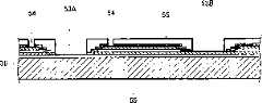
因此,为降低LSI与去耦电容器之间的线长,如图1所示,提出一种在转接板502的表面上设置由薄膜电容器构成的去耦电容器505的方法,其中,在转接板502的Si衬底503中形成通路508(例如,参见日本专利申请特开No.2004-193614)。Therefore, in order to reduce the line length between the LSI and the decoupling capacitor, as shown in FIG.
上述方法在高性能LSI中有效。这是因为转接板502采用由与LSI相同的材料构成的Si衬底503,所以不会发生由热膨胀不同引发应力所导致的问题。还因为该方法适用于LSI尺寸的增加、节距(pitch)的减小、以及由于低k LSI互连绝缘膜导致的强度下降。The above method is effective in high-performance LSIs. This is because the
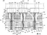
图1为传统半导体器件500的横截面图。如图1所示,半导体器件500包括高频运行的半导体芯片501以及与半导体芯片501连接的转接板502。FIG. 1 is a cross-sectional view of a
转接板502包括Si衬底503、去耦电容器505、绝缘膜507、通路508、以及外部连接端子(terminal)509。去耦电容器505形成于Si衬底503上,每个去耦电容器505由下电极、介电膜和上电极构成。去耦电容器505连接至一些连接至半导体芯片501的电源电极焊盘(pad)的通路508以及其它连接至半导体芯片501的接地电极焊盘的通路508。去耦电容器505消除由高频运行的半导体芯片所产生的噪声。The
用于形成通路508的通孔504形成于硅衬底503中。绝缘膜507形成于通孔504上。绝缘膜507将通路508与Si衬底503隔离。通常,使用热氧化膜作为绝缘膜507。A
通路508形成于通孔504中。在通路508的下端部形成用于连接至电路板的外部连接端子509(例如,参见日本专利申请特开No.2004-193614)。
当制造这种半导体器件500时,在Si衬底503中形成通孔504及通路508之后,在Si衬底503上形成去耦电容器505。When manufacturing such a
关于相关技术,也可参考日本专利申请特开No.2000-323845、2004-71589、2004-95638、2003-197463、及2004-273825。Regarding related technologies, Japanese Patent Application Laid-Open Nos. 2000-323845, 2004-71589, 2004-95638, 2003-197463, and 2004-273825 can also be referred to.
但是,传统转接板502的Si衬底503的厚度大于或等于0.5mm。因此,通孔504的孔径比(即Si衬底503的厚度/通孔504的直径)较高。为形成这些通孔504,需要使用ICP(感应耦合等离子体),这将导致半导体器件500的制造成本增加的问题。将来如果半导体芯片501的外部连接端子509的节距更窄,则更难以形成通孔504。However, the thickness of the
此外,传统上在形成通孔504之后,在Si衬底503上形成由薄膜电容器构成的去耦电容器505。这将引发不易隔离去耦电容器505的问题,从而导致成品率下降。Furthermore, a decoupling
此外,由于单层结构的薄膜电容器的电容有限,因此期望通过设置多层结构的薄膜电容器增加电容。但是,这将导致成本较高的问题,因为需要为每层形成并图案化电极和介电膜。此外,由于薄膜电容器形成于图案化的不平坦底层上,因此存在由于介电膜的膜厚不均匀以及灰尘引起的成品率较低的问题,导致成本增加。In addition, since the capacitance of a film capacitor of a single layer structure is limited, it is desired to increase the capacitance by providing a film capacitor of a multilayer structure. However, this leads to a problem of high cost because electrodes and dielectric films need to be formed and patterned for each layer. In addition, since the thin film capacitor is formed on a patterned uneven substrate, there is a problem of low yield due to uneven film thickness of the dielectric film and dust, resulting in an increase in cost.
发明内容Contents of the invention
因此,本发明的总的目的是提供消除上述缺点的半导体器件。It is therefore a general object of the present invention to provide a semiconductor device in which the above-mentioned disadvantages are eliminated.
本发明的更具体目的是提供可高频运行及可低成本制造的半导体器件。A more specific object of the present invention is to provide a semiconductor device which can operate at high frequency and which can be manufactured at low cost.
本发明的另一更具体目的是提供制造该半导体器件的方法。Another more specific object of the present invention is to provide a method of manufacturing the semiconductor device.
本发明的另一更具体目的是提供该半导体器件中所采用的电容器结构及该电容器结构的制造方法。Another more specific object of the present invention is to provide a capacitor structure used in the semiconductor device and a manufacturing method of the capacitor structure.
通过包括转接板和半导体芯片的半导体器件实现本发明的一个或更多上述目的,该转接板包括:Si衬底;多个通路,这些通路通过绝缘材料在穿过该Si衬底的相应通孔中设置;薄膜电容器,设置于该Si衬底的第一主表面上,以使其电连接至通路;以及多个外部连接端子,设置于该Si衬底的第二主表面上,以使其电连接至通路,该第二主表面背对该第一主表面;该半导体芯片设置于该第一主表面或该第二主表面上,以使其电连接至通路,其中该Si衬底的厚度小于通孔的直径。One or more of the above-mentioned objects of the present invention are achieved by a semiconductor device comprising an interposer and a semiconductor chip, the interposer comprising: a Si substrate; provided in a through hole; a film capacitor provided on the first main surface of the Si substrate so as to be electrically connected to the via; and a plurality of external connection terminals provided on the second main surface of the Si substrate to making it electrically connected to the via, the second main surface facing away from the first main surface; the semiconductor chip is disposed on the first main surface or the second main surface so as to be electrically connected to the via, wherein the Si substrate The thickness of the bottom is smaller than the diameter of the through hole.
按照本发明的一个方案,转接板的Si衬底的厚度小于或等于通孔的直径。因而,可实现具有良好精确度的通孔并可支持密度进一步增加的半导体器件。此外,由于靠近半导体芯片设置薄膜电容器,可实现具有减小的等效串联电感的半导体器件,从而使得该半导体芯片能够高频运行。此外,由于易于形成通孔,可实现以低成本制造的廉价半导体器件。According to a solution of the present invention, the thickness of the Si substrate of the interposer is smaller than or equal to the diameter of the through hole. Thus, via holes with good precision can be realized and further increased density of semiconductor devices can be supported. Furthermore, since the film capacitor is disposed close to the semiconductor chip, a semiconductor device having a reduced equivalent series inductance can be realized, thereby enabling the semiconductor chip to operate at a high frequency. In addition, since via holes are easily formed, an inexpensive semiconductor device manufactured at low cost can be realized.
通过下述半导体器件的制造方法也可实现本发明的一个或更多上述目的,该半导体器件包括转接板和半导体芯片,该转接板包括:Si衬底;多个通路,这些通路通过绝缘材料在穿过该Si衬底的相应通孔中设置;薄膜电容器,设置于该Si衬底的第一主表面上,以使其电连接至通路;以及多个外部连接端子,设置于该Si衬底的第二主表面上,以使其电连接至通路,该第二主表面背对该第一主表面;该半导体芯片电连接至通路,所述方法包括如下步骤:(a)形成该薄膜电容器;(b)薄化该Si衬底;以及(c)在该薄化的Si衬底中形成通孔。One or more of the above objects of the present invention can also be achieved by a method of manufacturing a semiconductor device comprising an interposer and a semiconductor chip, the interposer comprising: a Si substrate; materials are provided in corresponding via holes through the Si substrate; film capacitors are provided on the first main surface of the Si substrate so as to be electrically connected to vias; and a plurality of external connection terminals are provided on the Si substrate. The second main surface of the substrate, so that it is electrically connected to the via, the second main surface faces away from the first main surface; the semiconductor chip is electrically connected to the via, the method comprising the steps of: (a) forming the thin film capacitor; (b) thinning the Si substrate; and (c) forming via holes in the thinned Si substrate.
按照本发明的一个方案,通过执行薄化Si衬底的步骤,可降低通孔的孔径比(Si衬底厚度/通孔直径),因此可在Si衬底中容易地形成通孔。因而,能够降低半导体器件的制造成本。此外,由于在形成通孔的步骤之前执行形成薄膜电容器的步骤,能够高温形成薄膜电容器的介电膜。因而,能够形成高介电常数、大电容及高可靠性的薄膜电容器。According to an aspect of the present invention, by performing the step of thinning the Si substrate, the aperture ratio (Si substrate thickness/via diameter) of the via hole can be reduced, so that the via hole can be easily formed in the Si substrate. Thus, the manufacturing cost of the semiconductor device can be reduced. Furthermore, since the step of forming the thin film capacitor is performed before the step of forming the via hole, the dielectric film of the thin film capacitor can be formed at a high temperature. Therefore, it is possible to form a film capacitor with a high dielectric constant, large capacitance, and high reliability.
通过包括电路板及半导体芯片的半导体器件也可实现本发明的一个或更多上述目的,其中该电路板包括:多层互连结构;电容器结构,其包括位于该多层互连结构上的薄膜电容器;绝缘膜,其覆盖该电容器结构;通路,其穿过该电容器结构,以使其电连接至该薄膜电容器和该多层互连结构;该半导体芯片电连接至该电路板上的通路;并且该电容器结构包括:Si衬底,其位于该多层互连结构上;通孔,其中形成通路,这些通孔穿过该Si衬底;以及该薄膜电容器,其形成于该Si衬底上,该Si衬底的厚度小于通孔的直径。One or more of the above objects of the present invention are also achieved by a semiconductor device comprising a circuit board comprising: a multilayer interconnection structure; a capacitor structure comprising a thin film on the multilayer interconnection structure and a semiconductor chip capacitor; an insulating film covering the capacitor structure; a via passing through the capacitor structure so that it is electrically connected to the film capacitor and the multilayer interconnection structure; the semiconductor chip is electrically connected to the via on the circuit board; And the capacitor structure includes: a Si substrate on the multilayer interconnection structure; vias in which vias are formed, the vias passing through the Si substrate; and the film capacitor formed on the Si substrate , the thickness of the Si substrate is smaller than the diameter of the via hole.
按照本发明的一个方案,电容器结构的Si衬底的厚度小于或等于通孔的直径。因而,可实现这样的半导体器件,其具有包含良好精确度的通孔的电容器结构,并可支持密度的进一步增加。此外,由于靠近半导体芯片设置薄膜电容器,可实现具有减小的等效串联电感的半导体器件,从而使得半导体芯片能够高频运行。According to one aspect of the present invention, the thickness of the Si substrate of the capacitor structure is less than or equal to the diameter of the via hole. Thus, a semiconductor device having a capacitor structure including via holes with good precision can be realized and can support a further increase in density. Furthermore, since the film capacitor is disposed close to the semiconductor chip, a semiconductor device with reduced equivalent series inductance can be realized, thereby enabling the semiconductor chip to operate at a high frequency.
通过下述半导体器件的制造方法也可实现本发明的一个或更多上述目的,该半导体器件包括电路板和半导体芯片,该电路板包括:多层互连结构;电容器结构,其包括位于该多层互连结构上的薄膜电容器;绝缘膜,其覆盖该电容器结构;通路,其穿过该电容器结构,以使其电连接至该薄膜电容器和该多层互连结构;该半导体芯片电连接至该电路板上的通路,该方法包括如下步骤:(a)在Si衬底上形成薄膜电容器多层体;(b)薄化该Si衬底;(c)形成穿过该薄膜电容器多层体和该Si衬底的通孔,以及(d)将包括该薄膜电容器多层体和该Si衬底的电容器结构应用至该多层互连结构。One or more of the above objects of the present invention can also be achieved by a method of manufacturing a semiconductor device comprising a circuit board and a semiconductor chip, the circuit board comprising: a multilayer interconnection structure; a capacitor structure comprising A film capacitor on a layer interconnect structure; an insulating film covering the capacitor structure; a via passing through the capacitor structure so that it is electrically connected to the film capacitor and the multilayer interconnect structure; the semiconductor chip is electrically connected to The via on the circuit board, the method comprising the steps of: (a) forming a thin film capacitor multilayer body on a Si substrate; (b) thinning the Si substrate; (c) forming a multilayer body through the thin film capacitor and the through hole of the Si substrate, and (d) applying a capacitor structure including the thin film capacitor multilayer body and the Si substrate to the multilayer interconnection structure.
按照本发明的一个方案,通过执行薄化Si衬底的工艺,可降低通孔的孔径比(Si衬底厚度/通孔直径),因此可在Si衬底中容易地形成通孔。因而,能够降低半导体器件的制造成本。此外,在形成通孔之前形成薄膜电容器。因此能够高温形成薄膜电容器的介电膜,从而能够实现高介电常数、大电容及高可靠性的薄膜电容器。According to an aspect of the present invention, by performing a process of thinning the Si substrate, the aperture ratio (Si substrate thickness/via diameter) of the via hole can be reduced, and thus the via hole can be easily formed in the Si substrate. Thus, the manufacturing cost of the semiconductor device can be reduced. In addition, film capacitors are formed before forming via holes. Therefore, the dielectric film of the film capacitor can be formed at a high temperature, and a film capacitor with a high dielectric constant, large capacitance, and high reliability can be realized.
通过下述电容器结构也可实现本发明的一个或更多上述目的,该电容器结构包括:衬底;薄膜电容器,其包括至少三个电极层和设置于所述至少三个电极层中的每两个相邻电极层之间的介电膜,所述至少三个电极层和介电膜堆叠于该衬底上;以及一对第一焊盘电极和第二焊盘电极(pad electrode),该第一焊盘电极和第二焊盘电极以预定间隔彼此隔开并用作该薄膜电容器的外部连接端子,其中该第一焊盘电极电连接至从该衬底侧计数的所述至少三个电极层中的奇数电极层;该第二焊盘电极电连接至从该衬底侧计数的所述至少三个电极层中的一个或更多偶数电极层,以及在该第一焊盘电极与该第二焊盘电极之间并联连接基本上具有相同电容的多个叠置电容器。One or more of the above-mentioned objects of the present invention can also be achieved by a capacitor structure comprising: a substrate; a film capacitor comprising at least three electrode layers and every two electrode layers disposed in the at least three electrode layers a dielectric film between two adjacent electrode layers, the at least three electrode layers and the dielectric film are stacked on the substrate; and a pair of first pad electrode and second pad electrode (pad electrode), the A first pad electrode and a second pad electrode are spaced apart from each other at a predetermined interval and serve as external connection terminals of the film capacitor, wherein the first pad electrode is electrically connected to the at least three electrodes counted from the substrate side the odd-numbered electrode layer in the layer; the second pad electrode is electrically connected to one or more even-numbered electrode layers of the at least three electrode layers counted from the substrate side, and between the first pad electrode and the A plurality of stacked capacitors having substantially the same capacitance are connected in parallel between the second pad electrodes.
按照本发明的一个方案,第一焊盘电极电连接至从衬底侧计数的奇数电极,并且第二焊盘电极电连接至从衬底侧计数的一个或多个偶数电极,从而在第一焊盘电极与第二焊盘电极之间并联连接基本上具有相同电容的多个电容器。因而,通过减少配置去耦电容器所需的互连线长而降低电感,能够实现阻抗降低的电容器结构。According to one aspect of the present invention, the first pad electrode is electrically connected to odd-numbered electrodes counted from the substrate side, and the second pad electrode is electrically connected to one or more even-numbered electrodes counted from the substrate side, so that at the first A plurality of capacitors having substantially the same capacitance are connected in parallel between the pad electrode and the second pad electrode. Thus, a capacitor structure with reduced impedance can be realized by reducing the inductance by reducing the length of the interconnection line required to arrange the decoupling capacitor.
通过下述电容器结构的制造方法可实现本发明的一个或更多的上述目的,该电容器结构包括:薄膜电容器,其设置于衬底上;以及一对第一焊盘电极和第二焊盘电极,该第一焊盘电极和第二焊盘电极以预定间隔彼此隔开并用作该薄膜电容器的外部连接端子,该方法包括如下步骤:(a)通过交替堆叠至少三个电极层和介电膜在该衬底上形成具有至少三个电极层的多层体;(b)在将形成该第一焊盘电极的位置形成第一垂直互连线部分,在将形成该第二焊盘电极的位置形成第二垂直互连线部分;以及(c)形成分别与该第一垂直互连线部分和该第二垂直互连线部分接触的该第一焊盘电极和该第二焊盘电极,其中步骤(b)包括如下步骤:(d)在将形成该第一焊盘电极的位置从该多层体的表面形成第一开口部分,该第一开口部分暴露从该衬底侧计数的至少三个电极层中的第一电极层;(e)在将形成该第二焊盘电极的位置从该多层体的表面形成第二开口部分,该第二开口部分暴露从该衬底侧计数的至少三个电极层中的第二电极层;(f)形成覆盖该第一开口部分、该第二开口部分和至少三个电极层中的最上方电极层的绝缘膜;以及(g)在对应于将形成该第一焊盘电极的位置的绝缘膜部分形成第一互连线部分,该第一互连线部分包括与从该衬底侧计数的至少三电极层中的该第一电极层以及其余一个或多个奇数电极层接触的多条垂直互连线,并在对应于将形成该第二焊盘电极的位置的绝缘膜部分形成第二互连线部分,该第二互连线部分包括与从该衬底侧计数的至少三电极层中的一个或多个偶数电极层接触的一条或多条垂直互连线。One or more of the above objects of the present invention can be achieved by a method of manufacturing a capacitor structure comprising: a film capacitor provided on a substrate; and a pair of first pad electrodes and second pad electrodes , the first pad electrode and the second pad electrode are spaced apart from each other at predetermined intervals and used as external connection terminals of the film capacitor, the method comprising the steps of: (a) by alternately stacking at least three electrode layers and a dielectric film A multilayer body having at least three electrode layers is formed on the substrate; (b) forming a first vertical interconnect line portion where the first pad electrode will be formed, and where the second pad electrode will be formed and (c) forming the first pad electrode and the second pad electrode in contact with the first vertical interconnect portion and the second vertical interconnect portion, respectively, Wherein step (b) includes the following steps: (d) forming a first opening portion from the surface of the multilayer body at the position where the first pad electrode will be formed, the first opening portion exposing at least The first electrode layer among the three electrode layers; (e) forming a second opening portion from the surface of the multilayer body at the position where the second pad electrode will be formed, the second opening portion exposing the second opening portion to be counted from the substrate side (f) forming an insulating film covering the first opening portion, the second opening portion, and the uppermost electrode layer among the at least three electrode layers; and (g) A portion of the insulating film corresponding to a position where the first pad electrode is to be formed forms a first interconnection portion including the first electrode in at least three electrode layers counted from the substrate side. layer and the remaining one or more odd-numbered electrode layers contact a plurality of vertical interconnection lines, and form a second interconnection line portion in the insulating film portion corresponding to the position where the second pad electrode will be formed, the second interconnection The line portion includes one or more vertical interconnection lines in contact with one or more even-numbered electrode layers among at least three electrode layers counted from the substrate side.
按照本发明的一个方案,通过第一开口部分和第二开口部分暴露三个或更多电极层。通过包括多条互连线的第一互连线部分电连接在第一开口部分暴露的第一焊盘电极和从衬底侧计数的奇数电极层,并通过包括多条互连线的第二互连线部分电连接在第二开口部分暴露的第二焊盘电极和从该衬底侧计数的一个或多个偶数电极层。结果,能够利用比传统线长短的互连线长并联连接多个叠置电容器。因而,电感降低,从而能够实现阻抗降低的电容器结构。According to an aspect of the present invention, three or more electrode layers are exposed through the first opening portion and the second opening portion. The first pad electrode exposed at the first opening part and the odd-numbered electrode layers counted from the substrate side are electrically connected through the first interconnection line part including a plurality of interconnection lines, and the second pad electrode layer including a plurality of interconnection lines is electrically connected. The interconnection line portion electrically connects the second pad electrode exposed at the second opening portion and one or more even-numbered electrode layers counted from the substrate side. As a result, a plurality of stacked capacitors can be connected in parallel with an interconnection line length shorter than conventional line lengths. Therefore, the inductance is reduced, and a capacitor structure with reduced impedance can be realized.
通过包含转接板的半导体器件也可实现本发明的一个或更多上述目的,该转接板包括:Si衬底;薄膜电容器,其包括至少三个电极层和设置于至少三个电极层的每两个相邻电极层之间的介电膜,所述至少三个电极层和介电膜堆叠在该Si衬底上;多个通路,这些通路穿过该Si衬底;以及一对第一焊盘电极和第二焊盘电极,该第一焊盘电极和第二焊盘电极在覆盖该薄膜电容器的绝缘膜上以预定间隔彼此隔开并电连接至相应的通路,其中该第一焊盘电极电连接至从该Si衬底侧计数的至少三个电极层中的奇数电极层;该第二焊盘电极电连接至从该Si衬底侧计数的至少三个电极层中的一个或多个偶数电极层;并且在该第一焊盘电极与该第二焊盘电极之间并联连接基本上具有相同电容的多个电容器。One or more of the above-mentioned objects of the present invention can also be achieved by a semiconductor device comprising an interposer comprising: a Si substrate; a film capacitor comprising at least three electrode layers and a film capacitor disposed on the at least three electrode layers A dielectric film between every two adjacent electrode layers, the at least three electrode layers and the dielectric film are stacked on the Si substrate; a plurality of vias passing through the Si substrate; and a pair of first a pad electrode and a second pad electrode, the first pad electrode and the second pad electrode are spaced apart from each other at a predetermined interval on the insulating film covering the thin film capacitor and are electrically connected to corresponding vias, wherein the first pad electrode The pad electrode is electrically connected to an odd-numbered electrode layer in at least three electrode layers counted from the Si substrate side; the second pad electrode is electrically connected to one of the at least three electrode layers counted from the Si substrate side or a plurality of even-numbered electrode layers; and a plurality of capacitors having substantially the same capacitance are connected in parallel between the first pad electrode and the second pad electrode.
按照本发明的一个方案,第一焊盘电极电连接至从衬底侧计数的奇数电极,并且第二焊盘电极电连接至从衬底侧计数的的一个或多个偶数电极,从而在第一焊盘电极与第二焊盘电极之间并联连接基本上具有相同电容的多个电容器。因而,通过减少配置去耦电容器所需的互连线长而降低电感,能够实现阻抗降低的电容器结构。According to one aspect of the present invention, the first pad electrode is electrically connected to odd-numbered electrodes counted from the substrate side, and the second pad electrode is electrically connected to one or more even-numbered electrodes counted from the substrate side, so that A plurality of capacitors having substantially the same capacitance are connected in parallel between the first pad electrode and the second pad electrode. Thus, a capacitor structure with reduced impedance can be realized by reducing the inductance by reducing the length of the interconnection line required to arrange the decoupling capacitor.
通过下述半导体器件的制造方法也可实现本发明的一个或更多的上述目的,该半导体器件包括:薄膜电容器,其设置于Si衬底上;多个通路,这些通路穿过该Si衬底;以及一对第一焊盘电极和第二焊盘电极,该第一焊盘电极和第二焊盘电极在覆盖该薄膜电容器的绝缘膜上以预定间隔彼此隔开并电连接至相应的通路,该方法包括如下步骤:(a)通过交替堆叠至少三个电极层和介电膜在该Si衬底上形成具有至少三个电极层的多层体;(b)在将形成该第一焊盘电极的位置形成第一垂直互连线部分,在将形成该第二焊盘电极的位置形成第二垂直互连线部分;以及(c)形成分别与该第一垂直互连线部分和该第二垂直互连线部分接触的该第一焊盘电极和该第二焊盘电极,其中步骤(b)包括如下步骤:(d)在将形成该第一焊盘电极的位置从该多层体的表面形成第一开口部分,该第一开口部分暴露从该Si衬底侧计数的至少三个电极层中的第一电极层;(e)在将形成该第二焊盘电极的位置从该多层体的表面形成第二开口部分,该第二开口部分暴露从该Si衬底侧计数的至少三个电极层中的第二电极层;(f)形成覆盖该第一开口部分、该第二开口部分和至少三个电极层中的最上方电极层的绝缘膜;以及(g)在对应于将形成该第一焊盘电极的位置的绝缘膜部分形成第一互连线部分,该第一互连线部分包括与该第一电极层以及从该Si衬底侧计数的至少三个电极层中的其余一个或多个奇数电极层接触的多条垂直互连线,在对应于将形成该第二焊盘电极的位置的绝缘膜部分形成第二互连线部分,该第二互连线部分包括与从该Si衬底侧计数的至少三个电极层中的一个或多个偶数电极层接触的一条或多条垂直互连线。One or more of the above objects of the present invention can also be achieved by a method of manufacturing a semiconductor device comprising: a film capacitor provided on a Si substrate; a plurality of vias passing through the Si substrate ; and a pair of first pad electrode and second pad electrode, the first pad electrode and the second pad electrode are spaced apart from each other at a predetermined interval on the insulating film covering the thin film capacitor and are electrically connected to corresponding vias , the method includes the steps of: (a) forming a multilayer body having at least three electrode layers on the Si substrate by alternately stacking at least three electrode layers and a dielectric film; (b) forming the first solder forming a first vertical interconnection portion at the location of the pad electrode, and forming a second vertical interconnection portion at the location where the second pad electrode will be formed; and (c) forming the first vertical interconnection portion and the The first pad electrode and the second pad electrode partially contacted by the second vertical interconnection line, wherein step (b) includes the step of: (d) removing from the multilayer at the position where the first pad electrode is to be formed. A first opening portion is formed on the surface of the body, and the first opening portion exposes the first electrode layer among at least three electrode layers counted from the Si substrate side; (e) at the position where the second pad electrode will be formed from The surface of the multilayer body forms a second opening portion that exposes a second electrode layer among at least three electrode layers counted from the Si substrate side; (f) forming a second opening portion covering the first opening portion, the The second opening portion and the insulating film of the uppermost electrode layer among the at least three electrode layers; and (g) forming a first interconnection line portion at a portion of the insulating film corresponding to a position where the first pad electrode is to be formed, the The first interconnect line portion includes a plurality of vertical interconnect lines in contact with the first electrode layer and the remaining one or more odd-numbered electrode layers of at least three electrode layers counted from the Si substrate side, corresponding to the The insulating film portion at the position where the second pad electrode is formed forms a second interconnection portion including one or more even numbers of at least three electrode layers counted from the Si substrate side. One or more vertical interconnect lines to which the electrode layers are contacted.
附图说明Description of drawings
根据以下结合附图的详细说明,本发明的其它目的、特点和优点将更清楚,其中:According to the following detailed description in conjunction with the accompanying drawings, other objects, features and advantages of the present invention will be more clear, wherein:
图1为传统半导体器件的横截面图;1 is a cross-sectional view of a conventional semiconductor device;
图2为按照本发明第一实施例的电子器件的横截面图;2 is a cross-sectional view of an electronic device according to a first embodiment of the present invention;
图3A至图3L为按照本发明第一实施例的半导体器件制造方法的示意图;3A to 3L are schematic diagrams of a semiconductor device manufacturing method according to a first embodiment of the present invention;
图4为按照本发明第一实施例的第一变化例的半导体器件的横截面图;4 is a cross-sectional view of a semiconductor device according to a first modification of the first embodiment of the present invention;
图5A和图5B为按照本发明第一实施例的第一变化例的半导体器件制造方法的示意图;5A and 5B are schematic diagrams of a method for manufacturing a semiconductor device according to a first modification of the first embodiment of the present invention;
图6为按照本发明第一实施例的第二变化例的半导体器件的横截面图;6 is a cross-sectional view of a semiconductor device according to a second modification of the first embodiment of the present invention;
图7A和图7D为按照本发明第一实施例的第二变化例的半导体器件制造方法的示意图;7A and 7D are schematic diagrams of a semiconductor device manufacturing method according to a second variation of the first embodiment of the present invention;
图8为按照本发明第二实施例的半导体器件的横截面图;8 is a cross-sectional view of a semiconductor device according to a second embodiment of the present invention;
图9为按照本发明第三实施例的半导体器件的横截面图;9 is a cross-sectional view of a semiconductor device according to a third embodiment of the present invention;
图10为按照本发明第四实施例的半导体器件的横截面图;10 is a cross-sectional view of a semiconductor device according to a fourth embodiment of the present invention;
图11A至图11J为按照本发明第四实施例的半导体器件制造方法的示意图;11A to 11J are schematic views of a semiconductor device manufacturing method according to a fourth embodiment of the present invention;
图12A和图12B为按照本发明第四实施例的另一半导体器件制造方法的示意图;12A and 12B are schematic diagrams of another semiconductor device manufacturing method according to the fourth embodiment of the present invention;
图13为按照本发明第四实施例的第一变化例的半导体器件的横截面图;13 is a cross-sectional view of a semiconductor device according to a first modification of the fourth embodiment of the present invention;
图14为按照本发明第四实施例的第二变化例的半导体器件的横截面图;14 is a cross-sectional view of a semiconductor device according to a second modification of the fourth embodiment of the present invention;
图15为按照本发明第四实施例的第三变化例的半导体器件的横截面图;15 is a cross-sectional view of a semiconductor device according to a third modification of the fourth embodiment of the present invention;
图16为按照本发明第四实施例的第四变化例的半导体器件的横截面图;16 is a cross-sectional view of a semiconductor device according to a fourth modification of the fourth embodiment of the present invention;
图17为示出按照本发明第四实施例的第四变化例的垂直互连线的设置位置的电容器结构的俯视图;FIG. 17 is a top view of a capacitor structure showing the arrangement positions of vertical interconnection lines according to a fourth modification example of the fourth embodiment of the present invention;
图18为传统多层薄膜电容器的横截面图;18 is a cross-sectional view of a conventional multilayer film capacitor;
图19为示出在通过设置等同于图18所示的两个结构并联连接相同电容的两个电容器的情况下等效电路的电路图;FIG. 19 is a circuit diagram showing an equivalent circuit in a case where two capacitors of the same capacitance are connected in parallel by setting two structures equivalent to those shown in FIG. 18;
图20为按照本发明第五实施例的电容器结构的横截面图;20 is a cross-sectional view of a capacitor structure according to a fifth embodiment of the present invention;
图21为示出按照本发明第五实施例的垂直互连线的设置位置的电容器结构的俯视图;21 is a plan view of a capacitor structure showing the arrangement position of vertical interconnection lines according to a fifth embodiment of the present invention;
图22为示出按照本发明第五实施例在通过设置等同于图20所示的两个结构并联连接相同电容的两个电容器的情况下等效电路的电路图;22 is a circuit diagram showing an equivalent circuit in the case of connecting two capacitors of the same capacitance in parallel by setting two structures equivalent to those shown in FIG. 20 according to a fifth embodiment of the present invention;
图23A至图23I为按照本发明第五实施例的电容器结构制造方法的示意图;23A to 23I are schematic diagrams of a method for manufacturing a capacitor structure according to a fifth embodiment of the present invention;
图24为示出按照本发明第五实施例的薄膜电容器实例及其比较例的电极面积与缺陷率之间关系的图表;24 is a graph showing the relationship between the electrode area and the defect rate of an example of a film capacitor according to a fifth embodiment of the present invention and its comparative example;
图25为按照本发明第五实施例的第一变化例的电容器结构的横截面图;25 is a cross-sectional view of a capacitor structure according to a first modification of the fifth embodiment of the present invention;
图26为示出按照本发明第五实施例的第一变化例的垂直互连线的设置位置的示意图;FIG. 26 is a schematic diagram showing the arrangement positions of vertical interconnection lines according to the first modification example of the fifth embodiment of the present invention;
图27为按照本发明第五实施例的第二变化例的电容器结构的横截面图;27 is a cross-sectional view of a capacitor structure according to a second modification of the fifth embodiment of the present invention;
图28为按照本发明第五实施例的第三变化例的电容器结构的横截面图;28 is a cross-sectional view of a capacitor structure according to a third variation of the fifth embodiment of the present invention;
图29为按照本发明第五实施例安装电容器结构的实施例的示意图;Fig. 29 is a schematic diagram of an embodiment of installing a capacitor structure according to the fifth embodiment of the present invention;
图30为按照本发明第六实施例的半导体器件的横截面图;30 is a cross-sectional view of a semiconductor device according to a sixth embodiment of the present invention;
图31为按照本发明第六实施例安装半导体器件的实施例的示意图;31 is a schematic diagram of an embodiment of mounting a semiconductor device according to a sixth embodiment of the present invention;
图32A至图32P为按照本发明第六实施例的半导体器件制造方法的示意图;32A to 32P are schematic views of a semiconductor device manufacturing method according to a sixth embodiment of the present invention;
图33为按照本发明第七实施例的包含内置转接板的衬底(含转接板的衬底)的横截面图;以及33 is a cross-sectional view of a substrate including a built-in interposer (interposer-containing substrate) according to a seventh embodiment of the present invention; and
图34为按照本发明第七实施例安装含转接板的衬底的实施例的示意图。FIG. 34 is a schematic diagram of an embodiment of mounting a substrate including an interposer plate according to a seventh embodiment of the present invention.
具体实施方式Detailed ways
以下参照附图说明本发明的实施例。Embodiments of the present invention will be described below with reference to the drawings.
【第一实施例】【The first embodiment】
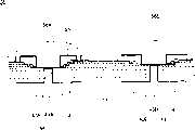
图2为按照本发明第一实施例的电子器件10的横截面图。FIG. 2 is a cross-sectional view of an electronic device 10 according to a first embodiment of the present invention.
参照图2,按照本实施例的电子器件包括半导体器件11及电路板12,半导体器件11安装于电路板12上。半导体器件11的多个外部连接端子44电连接至设置于电路板12上的相应连接焊盘13。Referring to FIG. 2 , the electronic device according to this embodiment includes a semiconductor device 11 and a circuit board 12 , and the semiconductor device 11 is mounted on the circuit board 12 . The plurality of
半导体器件11包括半导体芯片20和转接板30。半导体芯片20包括至少一个连接焊盘32A及至少一个连接焊盘32B。连接焊盘32A为用于电源的电极焊盘(电源电极焊盘),其连接至设置于转接板30的第一主表面侧上的相应内部连接端子56A。连接焊盘32B为用于接地的电极焊盘(接地电极焊盘),其连接至设置于转接板30的第一主表面侧上的相应内部连接端子56B。例如,以高频驱动的半导体芯片可用作本实施例中所采用的半导体芯片20。该半导体芯片20具有形成于硅衬底上的半导体电路,例如CPU、ROM、以及RAM。The semiconductor device 11 includes a
转接板30包括Si衬底36、绝缘材料39、金属膜41和55、通路43A和43B、外部连接端子44、绝缘膜45和52、至少一个薄膜电容器46、保护膜51、以及内部连接端子56A和56B。
Si衬底36为薄板。在Si衬底36中对应于通路43A和43B的形成位置的位置形成直径为R1的通孔38。将通孔38形成为使其直径R1大于通路43A和43B的直径。The
由此,通过将通孔38形成为使其直径R1大于通路43A和43B的直径,能够在Si衬底36与通路43A和43B之间容易地形成一层绝缘材料39。Thus, a layer of insulating
此外,薄Si衬底36的厚度M1小于通孔38的直径R1。因此,通过在薄Si衬底36中形成直径R1大于通路43A和43B的直径的通孔38,能够形成孔径比减小的良好通孔38。Furthermore, the thickness M1 of the
通孔38的直径R1例如可为100μm。形成通孔38的节距例如可为150μm至250μm。通孔38的直径R1和节距并不限于上述数值。The diameter R1 of the through
此外,优选地,Si衬底36的厚度M1在30μm至100μm的范围内。在厚度M1小于30μm的情况下,Si衬底36的强度不足。如果厚度M1大于100μm,通孔38的孔径比(M1/R1)变高,因此难以形成通孔38。Furthermore, preferably, thickness M1 of
将绝缘材料39形成为填充Si衬底36与通路43A和43B之间的对应于通孔38的空隙,并覆盖Si长度36的下表面36B。在绝缘材料39中对应于通孔38的位置形成通孔40A和40B。通孔40A穿过绝缘材料39和绝缘膜45。通孔40B穿过绝缘材料39、绝缘膜45以及薄膜电容器46的下电极47。Insulating
在Si衬底36与通路43A和43B之间的绝缘材料39的厚度L例如可为0.05μm至50μm。此外,Si衬底36的下表面36B上的绝缘材料39的厚度N例如可为0.05μm至10μm。可采用低介电常数(低k)树脂、耐热树脂、或光敏树脂作为绝缘材料39的材料。优选地,采用介电常数为1.0至3.5的材料作为低k树脂。低k树脂的实例包括氟树脂,例如聚氟乙烯、氟化环氧树脂、以及氟化聚酰亚胺。耐热树脂的实例包括环氧树脂、聚酰亚胺树脂、以及联苯醚树脂。光敏树脂的实例包括光敏聚酰亚胺树脂。The thickness L of insulating
在利用上述低k树脂作为绝缘材料39的情况下,能够防止半导体器件11的信号衰减。In the case where the above-mentioned low-k resin is used as the insulating
在对应于外部连接端子44的形成位置的位置处的绝缘材料39的表面39A上及通孔40A和40B的表面上形成例如20nm厚的金属膜41。金属膜41电连接至形成于转接板30的第一主表面侧上的金属膜55。在通过电镀形成通路43A和43B以及外部连接端子44的过程中,金属膜41用作电源层。可采用通过顺序堆叠例如Ti膜、Cu膜和Ni膜所形成的多层膜作为金属膜41。A
在其上形成金属膜41的通孔40A和40B中分别形成例如直径为70μm的通路43A和43B。通路43A和43B与相应的外部连接端子44成为整体。通路43A电连接内部连接端子56A及相应的外部连接端子44。通路43B电连接内部连接端子56B及相应的外部连接端子44。可采用导电材料作为通路43A和43B的材料。具体地,例如可采用Sn-Ag焊料。
在设置于绝缘材料39的表面39A上的金属膜41上形成外部连接端子44。外部连接端子44电连接设置于电路板12上的连接焊盘13和通路43A、43B。可采用导电材料作为通路43A、43B的材料。例如,可采用Sn-Ag焊料作为导电材料。
在Si衬底36的上表面36A上形成例如50nm厚的绝缘膜45。绝缘膜45为薄膜电容器46的粘附层。可采用具有极佳耐湿性的绝缘膜作为绝缘膜45。例如,可采用SiO2膜或氧化铝膜作为绝缘膜45。On
薄膜电容器46包括介电膜48、下电极47和上电极49。介电膜48夹在下电极47与上电极49之间。下电极47、介电膜48和上电极49以所述顺序堆叠。The
薄膜电容器46形成于内部连接端子56A与内部连接端子56B之间的位置处的绝缘膜45上,内部连接端子56A和内部连接端子56B分别连接至半导体芯片20的电源电极焊盘32A和接地电极焊盘32B。上电极49电连接至内部连接端子56A。下电极47电连接至内部连接端子56B。通过如此电连接薄膜电容器46,薄膜电容器46起到去耦电容器的作用,以吸收由半导体芯片20产生的噪声。The
例如,可采用Au、Al、Pt、Ag、Pd、Cu及它们的合金作为下电极47的材料,下电极47的厚度可为100nm。For example, Au, Al, Pt, Ag, Pd, Cu and their alloys can be used as the material of the
厚度例如为100nm的介电膜48的材料没有特殊限制,只要其为介电材料即可。优选地,介电膜48由具有高介电常数的钙钛矿型晶体结构的金属氧化物材料构成。这种材料的实例包括(Ba,Sr)TiO3(BST)、SrTiO3(ST)、BaTiO3、Ba(Zr,Ti)O3、Ba(Ti,Sn)O3、Pb(Zr,Ti)O3(PZT)、(Pb,La)(Zr,Ti)O3(PLZT)、Pb(Mn,Nb)O3-PbTiO3(PMN-PT)、和Pb(Ni,Nb)O3-PbTiO3。The material of
在采用具有钙钛矿型晶体结构的金属氧化物材料作为介电膜48的情况下,优选采用Pt作为下电极47的材料。采用Pt能够使得介电膜48外延生长,从而增加介电膜48的介电常数。In the case of employing a metal oxide material having a perovskite-type crystal structure as the
作为上电极49的材料,可采用例如Au、Al、Pt、Ag、Pd、Cu及它们的合金。上述金属或其合金可堆叠于IrOx上。上电极49的厚度例如可为100nm。As the material of the
设置厚度例如为0.1μm的保护膜51,以覆盖薄膜电容器46。保护膜51由无特殊限制的绝缘材料构成,但该绝缘材料优选为具有极佳耐湿性的Si3N4、SiO2或氧化铝。采用这种材料能够防止具有钙钛矿型晶体结构的介电膜48的特性退化(degradation)。A
设置厚度例如为2μm的绝缘膜52以覆盖保护膜51。在绝缘膜52中形成暴露绝缘膜45的开口部分(孔)53A、暴露下电极47的开口部分(孔)53B、和位置靠近开口部分53A并暴露上电极49的开口部分(孔)54。绝缘膜52由与上述绝缘材料39相同的材料构成。An insulating
在对应于内部连接端子56A的形成位置的绝缘膜52的部分(包括开口部分53A和54的内表面)上及对应于内部连接端子56B的形成位置的绝缘膜52的部分(包括开口部分53B的内表面)上形成厚度例如为50nm的金属膜55。在通过电镀形成内部连接端子56A和56B的过程中,金属膜55用作电源层。可采用通过顺序堆叠例如Ti膜、Cu膜和Ni膜所形成的多层膜作为金属膜55。On the portion of the insulating
内部连接端子56A形成于金属膜55上,以填充开口部分53A和54并从绝缘膜52突起。内部连接端子56A为连接至半导体芯片20的电源电极焊盘32A的电源端子。内部连接端子56A电连接至通路43A和上电极49。内部连接端子56A的突起部分连接至半导体芯片20的电源电极焊盘32A。The
内部连接端子56B形成于金属膜55上,以填充开口部分53B并从绝缘膜52突起。内部连接端子56B为连接至半导体芯片20的接地电极焊盘32B的接地端子。内部连接端子56B电连接至通路43B和下电极47。内部连接端子56B的突起部分连接至半导体芯片20的接地电极焊盘32B。可采用导电材料作为内部连接端子56A和56B的材料。具体地,例如可采用Sn-Ag焊料。The
按照本实施例,转接板30的Si衬底36的厚度M1可小于或等于通孔38的直径R1。因此,可实现这样的半导体器件11,其具有良好精确度的通孔38和可支持密度进一步增加的转接板30。According to this embodiment, the thickness M1 of the
此外,由于靠近半导体芯片20设置薄膜电容器46,可降低等效串联电感。结果,可实现其中半导体芯片20可高频运行的半导体器件11。In addition, since the
在本实施例中,对薄膜电容器46用作去耦电容器的情况进行说明。可选地,薄膜电容器46可用作除了去耦电容器之外的电容器。并且,在本实施例中,以单层薄膜电容器46为例。可选地,可设置多层薄膜电容器取代单层薄膜电容器46,该多层薄膜电容器具有在下电极47与上电极49之间的至少两个介电膜48以及夹在相邻介电膜48之间的中间电极。中间电极的材料可与上电极49的材料相同。In this embodiment, a case where the
图3A至图3L为按照本发明第一实施例的半导体器件制造方法的示意图。以下参照附图说明按照本实施例的半导体器件11的制造方法。3A to 3L are schematic diagrams of a method of manufacturing a semiconductor device according to a first embodiment of the present invention. A method of manufacturing the semiconductor device 11 according to the present embodiment will be described below with reference to the drawings.
首先,在图3A的处理中,通过溅射形成作为粘附膜的绝缘膜45,并进一步在Si衬底36的表面(该Si衬底36在该表面上形成有热氧化膜(SiO2膜))上顺序形成下电极膜47A、介电膜48A和上电极膜49A。First, in the process of FIG. 3A, an insulating
具体地,例如使用多靶DC-RF磁控管溅射装置,在Si衬底36上形成非晶氧化铝膜(厚度为50nm)作为绝缘膜45,其中在衬底温度为200℃的情况下在Si衬底36上形成热氧化膜(SiO2膜)。接着,在衬底温度为200℃的情况下,形成Pt膜(厚度为100nm)作为下电极膜47A。接着,在衬底温度为600℃的情况下,形成BST膜(厚度为100nm)作为介电膜48A。接着,在衬底温度为25℃的情况下,顺序形成IrOx膜和Au膜(厚度为100nm)作为上电极膜49A。这些多层膜45、47A、48A和49A可通过溅射以外的方法(例如气相沉积或CVD)形成。Specifically, for example, using a multi-target DC-RF magnetron sputtering apparatus, an amorphous aluminum oxide film (with a thickness of 50 nm) is formed as the insulating
接下来,在图3B所示的处理中,通过离子铣削将堆叠的上电极膜49A、介电膜48A和下电极膜47A图案化,从而形成薄膜电容器46。接着,在氧气氛中热处理薄膜电容器46以去除热变形并将氧原子提供至介电膜48及IrOx膜的缺氧部分。通过分别图案化下电极膜47A、介电膜48A和上电极膜49A,形成薄膜电容器46的下电极47、介电膜48和上电极49。Next, in the process shown in FIG. 3B , the stacked
接下来,在图3C所示的处理中,形成覆盖薄膜电容器46及绝缘膜45的保护膜51。接着,通过离子铣削在保护膜51中形成暴露上电极49的开口部分(孔)51A。接着,在氧气氛中对保护膜51进行后退火(post-annealing)处理。具体说来,例如,通过利用RF磁控管溅射装置的溅射形成非晶氧化铝膜(厚度为0.1μm)作为保护膜51。保护膜51可通过溅射以外的方法(例如气相沉积或CVD)形成。Next, in the process shown in FIG. 3C ,
因而,通过在通孔形成处理之前形成薄膜电容器46,能够高温形成介电膜48,因此可以形成大电容、高可靠性及高介电常数的薄膜电容器46。此外,通过在均匀平坦的绝缘膜45上顺序堆叠下电极膜47A、介电膜48A和上电极膜49A,并图案化下电极膜47A、介电膜48A和上电极膜49A,形成薄膜电容器46。因此,能够增加薄膜电容器46的成品率。此外,可防止在形成通孔38、40A和40B以及通路43A和43B的过程中所产生的杂质粘附于薄膜电容器46的形成区。因此,能够增加薄膜电容器46的成品率。Therefore, by forming the
接下来,在图3D的处理中,形成绝缘膜52以覆盖图3C所示的结构。接着,形成暴露绝缘膜45的开口部分53A、暴露下电极47的开口部分53B和暴露上电极49的开口部分54。具体说来,例如,通过旋涂形成光敏聚酰亚胺树脂(厚度为2μm)作为绝缘膜52。通过曝光光敏聚酰亚胺树脂并将该光敏聚酰亚胺树脂显影,形成开口部分53A、53B和54。也可以通过旋涂以外的方法(例如喷射或浸渍)形成绝缘膜52。Next, in the process of FIG. 3D , an insulating
接下来,在图3E所示的处理中,在图3D所示的结构上形成作为电镀籽晶层的金属膜55。具体说来,例如,通过溅射处理顺序地形成Ti膜、Cu膜和Ni膜,以作为金属膜55。金属膜55可通过溅射以外的方法(例如气相沉积或CVD)形成。Next, in the process shown in FIG. 3E, a
接下来,在图3F的处理中,在金属膜55上形成抗蚀层66,该抗蚀层66暴露对应于内部连接端子56A和56B的形成区的部分金属膜55。接着,使用导电材料68填充开口部分53A、53B和54。导电材料68随后回流以作为内部连接端子56A和56B。具体说来,通过使用金属膜55作为电源层进行电镀使得Sn-Ag焊料沉积,形成导电材料68。Next, in the process of FIG. 3F , a resist layer 66 exposing a portion of the
接下来,在图3G所示的处理中,去除未被导电材料68覆盖的金属膜55的多余部分。其后,通过加热使导电材料68回流,以形成Sn-Ag焊料凸块的内部连接端子56A和56B。Next, in the process shown in FIG. 3G , the excess portion of the
接下来,在图3H所示的处理中,通过粘合带69将支撑衬底(holdingsubstrate)70粘附至图3G所示的结构的第一主表面侧(其上形成内部连接端子56A和56B的一侧),并从第二主表面侧薄化Si衬底36。具体说来,例如,使用研磨机将Si衬底36薄化至50μm厚。在薄化Si衬底36之后,去除粘合带69。例如,可采用通过紫外线照射降低其粘度的UV带作为粘合带69。例如,可采用研磨或蚀刻来薄化Si衬底36。作为研磨方法,可采用抛光(例如磨光和CMP)及切割(cutting)。作为蚀刻方法,可采用例如湿蚀刻和等离子体蚀刻。Next, in the process shown in FIG. 3H , a holding
因此,通过在形成通孔38之前薄化Si衬底36,能够降低通孔38的孔径比,并且能够使用成本低于ICP(感应耦合等离子体)的等离子体蚀刻或湿蚀刻形成通孔38。因而,能够以低成本制造半导体器件11。Therefore, by thinning the
接下来,在图3I的处理中,在Si衬底36中从其第二主表面侧形成直径R1的通孔38。具体说来,例如,可使用氟化氢和硝酸的液体混合物作为蚀刻液进行湿蚀刻来形成通孔38。也可以使用其它蚀刻液进行蚀刻或者采用等离子体蚀刻。通孔38的直径R1例如可为100μm。Next, in the process of FIG. 3I , a via
接下来,在图3J所示的处理中,应用绝缘材料39填充通孔38并覆盖Si衬底36的下表面36B,接着,将绝缘材料39硬化。具体说来,例如,通过旋涂方式涂敷环氧树脂(其为耐热树脂)作为绝缘材料39,其后,在200℃的温度下使该环氧树脂热固。也可以通过旋涂以外的方法(例如喷射或浸渍)涂敷绝缘材料39。Next, in the process shown in FIG. 3J , the insulating
因此,与分别形成设置于Si衬底36的下表面36B上的绝缘材料和填充通孔38的绝缘材料的情况相比,通过将绝缘材料39形成为使其同时覆盖Si衬底36的下表面36B和填充通孔38,能够简化半导体器件11的制造工艺。Therefore, compared with the case where the insulating material provided on the
通过采用树脂材料(例如低k树脂、耐热树脂、或光敏树脂)作为填充通孔38的绝缘材料39,能够容易地形成用于形成通路43A和43B的通孔40A和40B,因此能够以低成本制造半导体器件11。可分别设置Si衬底36的下表面36B上的绝缘材料和填充通孔38的绝缘材料。在这种情况下,设置于Si衬底36的下表面36B上的绝缘材料可不同于填充通孔38的绝缘材料。By adopting a resin material such as low-k resin, heat-resistant resin, or photosensitive resin as the insulating
接下来,在图3K的处理中,在填充通孔38的绝缘材料39中形成暴露金属膜55的直径为70μm的通孔40A和40B。具体说来,通过使用耐热树脂或低k树脂作为绝缘材料39进行ArF受激准分子激光器处理,形成通孔40A和40B。也可以使用ArF受激准分子激光器处理以外的激光处理方法、或等离子体蚀刻形成通孔40A和40B。在使用光敏树脂作为绝缘材料39的情况下,可通过曝光并显影对应于通孔40A和40B的部分绝缘材料39形成通孔40A和40B。Next, in the process of FIG. 3K , via
接下来,在图3L的步骤中,通过与图3E至3G所示的处理中相同的方法形成金属膜41、通路43A和43B、以及外部连接端子44。此时,同时形成通路43A和43B以及外部连接端子44。Next, in the step of FIG. 3L , the
因此,通过同时形成通路43A和43B以及外部连接端子44,能够简化半导体器件11的制造工艺并降低其制造成本。此外,通过在薄化Si衬底36之后形成通路43A和43B,可减小连接半导体芯片20与电路板12的通路43A和43B的长度。这使得能够在半导体芯片20与连接至外部连接端子44的电路板12(图2)之间高速传输高频信号。此外,在薄化的Si衬底36中形成通孔40A和40B。这可减少通路43A和43B的处理时间,因此能够降低制造成本。Therefore, by simultaneously forming the
接下来,例如使用切片机切割Si衬底36,从而形成转接板30。其后,半导体芯片20的连接焊盘32A和32B分别连接至转接板30的内部连接端子56A和56B,从而制造半导体器件11。Next, the
按照本实施例的制造方法,由于Si衬底36被薄化,在形成通孔38的过程中厚度方向的处理量减少。因而,可容易地形成通孔38,并且可减少处理时间。此外,能够通过湿蚀刻或等离子体蚀刻形成通孔38。因而,能够以比传统ICP低得多的成本形成通孔38。此外,在使用绝缘材料(例如,低k树脂、耐热树脂、或光敏树脂)填充通孔38的情况下,通过激光通路(via)处理形成用于通路43A和43B的通孔40A和40B,因而导致处理成本较低。因此,可以以低于传统方法的成本制造半导体器件11。According to the manufacturing method of this embodiment, since the
此外,按照本实施例的制造方法,在Si衬底36中形成通孔38之前形成薄膜电容器46。这有利于薄膜电容器46的形成。与通孔38形成于薄膜电容器46之前的传统制造方法相比,由于能够防止在通孔38的形成过程中所产生的灰尘和杂质对薄膜电容器46的不利影响(例如不良隔离),所以能够增加薄膜电容器46的成品率。Furthermore, according to the manufacturing method of the present embodiment, the
评估通过上述图3A至图3L的制造方法所完成的转接板的电特性和可靠性。使用各制造处理中所指定的条件完成该转接板。对于电特性而言,评估结果为电容密度为4μF/cm2、ESR(等效串联电阻)为0.01Ω、ESL(等效串联电感)为10pH、和耐压为20V或以上。这些结果证明能够形成具有薄膜电容器46(其具有大电容及减小的ESL)的转接板。The electrical characteristics and reliability of the interposer board completed by the above-mentioned manufacturing method of FIGS. 3A to 3L were evaluated. The interposer is completed using the conditions specified in each fabrication process. As for the electrical characteristics, the evaluation results were that the capacitance density was 4 μF/cm2 , the ESR (equivalent series resistance) was 0.01Ω, the ESL (equivalent series inductance) was 10 pH, and the withstand voltage was 20 V or more. These results demonstrate that an interposer can be formed with
在温度为121℃、相对湿度为85%、外加电压为3V、和测试时间为48小时的条件下执行高温高湿负荷测试。测试后的绝缘电阻大于或等于10MΩ,这证明转接板在高温高湿下也具有足够的可靠性。The high temperature and high humidity load test was performed under the conditions of a temperature of 121° C., a relative humidity of 85%, an applied voltage of 3 V, and a test time of 48 hours. The insulation resistance after the test is greater than or equal to 10MΩ, which proves that the adapter board also has sufficient reliability under high temperature and high humidity.
图4为按照本发明第一实施例的第一变化例的半导体器件80的横截面图。图4中,以相同的标号代表与第一实施例的半导体器件11的那些元件相同的元件,并省略其说明。4 is a cross-sectional view of a
参照图4,半导体器件80包括半导体芯片20和转接板75。除分别形成通路43A和43B与外部连接端子44、以及焊盘78形成于通路43A和43B与相应的外部连接端子44之间以外,半导体器件80的结构与第一实施例的半导体器件11相同。Referring to FIG. 4 , a
通过使用导电浆料填充通路40A和40B来形成通路43A和43B。例如,可使用碳、银或铜的导电颗粒与粘合剂的混合物作为导电浆料。The
焊盘78形成于绝缘材料39的表面39A上以电连接至相应的通路43A和43B以及外部连接端子44。可采用通过顺序堆叠例如Ti膜、Cu膜和Ni膜所形成的多层膜作为焊盘78。外部连接端子44形成于相应的焊盘78上以通过焊盘78电连接至通路43A和43B。Pads 78 are formed on the
图5A和5B为按照本发明第一实施例的第一变化例的半导体器件制造方法的示意图。以下参照附图说明半导体器件80的制造方法。5A and 5B are schematic diagrams of a method of manufacturing a semiconductor device according to a first modification of the first embodiment of the present invention. A method of manufacturing the
首先,通过上述图3A至图3K的处理形成通孔40A和40B。接着,在图5A的处理中,使用导电浆料填充通孔40A和40B。接着,将该导电浆料硬化,从而形成通路43A和43B。具体说来,通过丝网印刷涂敷导电浆料,其后,在200℃的温度下使该导电浆料热固。First, the via
接下来,在图5B的处理中,通过与图3E至图3G所示的处理中相同的方法,在绝缘材料39的表面39A上连续形成焊盘78和外部连接端子44。接着,通过切片方式切割Si衬底36,从而形成转接板75。其后,通过将半导体芯片20连接至该转接板75,制造图4所示的半导体器件80。Next, in the process of FIG. 5B , pads 78 and
按照该第一变化例的半导体器件80可产生与半导体器件11相同的效果。评估通过上述图3A至图3K、图5A、及图5B的制造方法所完成的按照第一变化例的转接板的电特性和可靠性。使用各制造处理中所指定的条件完成按照第一变化例的转接板。对于电特性而言,评估结果为电容密度为4F/cm2、ESR(等效串联电阻)为0.01Ω、ESL(等效串联电感)为10pH、和电介质强度为20V或以上。这些结果证明能够形成具有薄膜电容器46(其具有大电容及减小的ESL)的转接板。The
在温度为121℃、相对湿度为85%、外加电压为3V、和测试时间为48小时的条件下执行高温高湿负荷测试。测试后的绝缘电阻大于或等于10MΩ,这证明按照第一变化例的转接板在高温高湿下也具有足够的可靠性。The high temperature and high humidity load test was performed under the conditions of a temperature of 121° C., a relative humidity of 85%, an applied voltage of 3 V, and a test time of 48 hours. The insulation resistance after the test is greater than or equal to 10 MΩ, which proves that the adapter board according to the first variation example also has sufficient reliability under high temperature and high humidity.
图6为按照本发明第一实施例的第二变化例的半导体器件的横截面图。图6中,以相同的标号代表与第一实施例的半导体器件11中的那些元件相同的元件,并省略其说明。6 is a cross-sectional view of a semiconductor device according to a second modification of the first embodiment of the present invention. In FIG. 6 , the same elements as those in the semiconductor device 11 of the first embodiment are denoted by the same reference numerals, and descriptions thereof are omitted.
参照图6,半导体器件90包括半导体芯片20和转接板95。半导体器件90的结构基本等同于第一实施例的第一变化例的半导体器件80,不同之处在于:金属膜92形成于与通孔40A和40B对应的部分绝缘材料39和部分绝缘膜45上以及与焊盘93的形成位置对应的部分绝缘材料39上;通路43A和43B通过电镀形成;焊盘93形成于与通路43A和43B对应的金属膜92上以及通路43A和43B上;外部连接端子44设置于对应的焊盘93上。Referring to FIG. 6 , a
金属膜92形成于与焊盘93的形成区对应的绝缘材料39的部分表面39A上以及通孔40A和40B上。金属膜92电连接至通路43A和43B以及内部连接端子56A和56B。在通过电镀形成通路43A和43B以及焊盘93的过程中,金属膜92用作电源层。例如,可采用Ti、Cr或Cu作为金属膜92的材料。
形成焊盘93以覆盖形成于绝缘材料39的表面39A上的金属膜92以及通路43A和43B。例如,可采用Ni作为焊盘93的材料。
形成外部连接端子44以覆盖焊盘93。外部连接端子44通过焊盘93电连接至通路43A和43B。The
具有这种结构的半导体器件90也可产生与第一实施例的半导体器件11相同的效果。此外,对上述制造处理所形成的转接板95的电特性及可靠性的评估显示出与第一实施例的转接板30相同的良好结果。The
图7A至7D为按照本发明第一实施例的第二变化例的半导体器件制造方法的示意图。以下参照附图说明半导体器件90的制造方法。7A to 7D are schematic views of a semiconductor device manufacturing method according to a second modification of the first embodiment of the present invention. A method of manufacturing the
首先,通过上述图3A至图3I的处理薄化Si衬底36并形成通孔38。具体说来,薄化Si衬底36,并通过使用氯基气体进行等离子体蚀刻在Si衬底36中形成直径R1(=200μm)的通孔38。First, the
接下来,在图3J所示的处理中,具体说来,涂敷光敏聚酰亚胺树脂作为绝缘材料39以填充通孔38并覆盖Si衬底36的下表面36B。接着,通过紫外线硬化该光敏聚酰亚胺树脂。Next, in the process shown in FIG. 3J , specifically, a photosensitive polyimide resin is applied as the insulating
接下来,在图3K的处理中,具体说来,通过光刻技术曝光并显影对应于通孔40A和40B的形成区的部分绝缘材料39。接着,利用氟化氢溶液湿蚀刻对应于通孔40A和40B的形成区的部分绝缘膜45,从而形成直径为50μm的通孔40A和40B。Next, in the process of FIG. 3K , specifically, a portion of the insulating
在形成通孔40A和40B之后,在随后的图7A的步骤中,在通孔40A和40B上以及绝缘材料39的表面39A上形成金属膜92。接着,在金属膜92上形成用于暴露焊盘93及外部连接端子44的形成区的抗蚀层96。利用例如溅射、非电解电镀、气相沉积或CVD形成金属膜92。After forming the via
接下来,在图7B的处理中,在通孔40A和40B中形成通路43A和43B。具体说来,通过电镀将铜镀膜沉积在通孔40A和40B上,形成通路43A和43B。接着,在由抗蚀层96暴露的部分金属膜92及通路43A和43B上形成焊盘93。具体说来,通过电镀形成作为焊盘93的Ni膜。Next, in the process of FIG. 7B , vias 43A and 43B are formed in the through
接下来,在图7C的处理中,在焊盘93上形成导电材料98。具体说来,在焊盘93上形成Sn-Ag焊料的导电材料98。随后,导电材料98回流以用作外部连接端子44。Next, in the process of FIG. 7C ,
接下来,在图7D的处理中,去除未被焊盘93覆盖的金属膜92的多余部分。接着,通过加热使导电材料98回流,从而形成外部连接端子44。其后,通过切片方式切割Si衬底36,从而形成转接板95。通过将半导体芯片20连接至该转接板95,制造半导体器件90。Next, in the process of FIG. 7D , the excess portion of the
按照该第二变化例的半导体器件90可产生与第一实施例的半导体器件11相同的效果。对通过上述图3A至图3K、及图7A至图7D的制造方法所完成的按照第二变化例的转接板的电特性和可靠性的评估显示出如按照第一实施例的转接板30的相同良好结果。利用各制造处理中所指定的条件完成按照第二变化例的转接板。The
【第二实施例】【Second Embodiment】
图8为按照本发明第二实施例的半导体器件器件100的横截面图。在图8中,以相同的标号代表与第一实施例的半导体器件11中的那些元件相同的元件,并省略其说明。FIG. 8 is a cross-sectional view of a
参照图8,除设置作为无源元件的电阻元件102以外,按照本实施例的半导体器件100的结构与第一实施例的半导体器件11相同。Referring to FIG. 8, the
电阻元件102包括一对电极103和104以及电阻器105,并形成于转接板30上。电极103形成于绝缘膜52上,并电连接至内部连接端子56A。结果,电极103通过内部连接端子56A电连接至薄膜电容器46和相应的外部连接端子44。The
电极104形成于绝缘膜52上,并电连接至内部连接端子56B。结果,电极104通过内部连接端子56B电连接至薄膜电容器46和相应的外部连接端子44。The electrode 104 is formed on the insulating
将电阻器105形成为连接电极103与电极104。电阻器105对通过电极103与电极104之间的电流施加电阻。此外,可在内部连接端子56A与内部连接端子56B之间添加由导电材料构成的电感元件作为另一无源元件。例如,可采用弯曲状的电感元件。The resistor 105 is formed to connect the electrode 103 and the electrode 104 . Resistor 105 applies resistance to the current passing between electrode 103 and electrode 104 . Furthermore, an inductance element made of a conductive material may be added between the
因此,通过利用无源元件(其包括电阻元件102和电感元件)设置具有薄膜电容器46的半导体器件100,能够优化半导体器件100的阻抗并使半导体器件100高频运行。Therefore, by arranging the
【第三实施例】[Third embodiment]
图9为按照本发明第三实施例的半导体器件110的横截面图。参照图9,半导体器件110包括:半导体衬底111,其上形成半导体电路112(内部电路);穿过半导体衬底111的通路113;以及形成于每个通路113的相应端的外部连接端子114和115。半导体电路112可包括有源元件。FIG. 9 is a cross-sectional view of a semiconductor device 110 according to a third embodiment of the present invention. 9, a semiconductor device 110 includes: a semiconductor substrate 111 on which a semiconductor circuit 112 (internal circuit) is formed; vias 113 passing through the semiconductor substrate 111; and external connection terminals 114 and 114 formed at respective ends of each via 113; 115. The semiconductor circuit 112 may include active elements.
半导体衬底111为薄板。半导体衬底111的厚度M2与第一实施例所述的Si衬底36的厚度M1的数值相同。The semiconductor substrate 111 is a thin plate. The thickness M2 of the semiconductor substrate 111 is the same value as the thickness M1 of the
半导体电路112电连接至通路113。通过如第一实施例所述(图3H至图3K)的通路43A和43B的相同方法形成通路113。即,在半导体衬底111薄化之后形成通路113。结果,与第一实施例的半导体器件11一样,可容易地形成用于形成通路113的通孔。可采用与第一实施例所述的通路43A和43B相同的材料作为通路113的材料。此外,可将其内形成通路113的通孔的直径形成为例如70μm。The semiconductor circuit 112 is electrically connected to the via 113 . The via 113 is formed by the same method as the
在相应的通路113的上端形成外部连接端子114。在相应的通路113的下端形成外部连接端子115。外部连接端子114通过通路113电连接至相应的外部连接端子115。将外部连接端子114和115设置为用于连接至其它半导体器件118和119。与半导体器件110一样,半导体器件118和119均具有薄化的半导体衬底、通路113、以及外部连接端子114和115。External connection terminals 114 are formed at upper ends of the corresponding vias 113 . External connection terminals 115 are formed at lower ends of the corresponding vias 113 . The external connection terminals 114 are electrically connected to corresponding external connection terminals 115 through vias 113 . External connection terminals 114 and 115 are provided for connection to other semiconductor devices 118 and 119 . Like the semiconductor device 110 , the semiconductor devices 118 and 119 each have a thinned semiconductor substrate, a via 113 , and external connection terminals 114 and 115 .
按照本实施例的半导体器件110,在薄化的半导体衬底111中形成通路113。因而,易于在半导体衬底111中形成通路113。此外,设置穿过半导体衬底111的通路113及形成于通路113的相应端的外部连接端子114和115。这使得能够多层连接其它半导体器件118和119,因此能够增加半导体器件110的封装密度。According to the semiconductor device 110 of the present embodiment, the via 113 is formed in the thinned semiconductor substrate 111 . Thus, it is easy to form the via 113 in the semiconductor substrate 111 . Furthermore, a via 113 penetrating the semiconductor substrate 111 and external connection terminals 114 and 115 formed at respective ends of the via 113 are provided. This enables multilayer connection of other semiconductor devices 118 and 119 , thus enabling an increase in the packing density of the semiconductor device 110 .
【第四实施例】[Fourth embodiment]
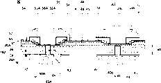
图10为按照本发明第四实施例的半导体器件120的横截面图。在图10中,以相同的标号代表与第一实施例的半导体器件11的那些元件相同的元件,并省略其说明。FIG. 10 is a cross-sectional view of a semiconductor device 120 according to a fourth embodiment of the present invention. In FIG. 10 , the same elements as those of the semiconductor device 11 of the first embodiment are denoted by the same reference numerals, and descriptions thereof are omitted.
参照图10,按照本实施例的半导体器件120包括半导体芯片20和其上安装半导体芯片20的电路板121。Referring to FIG. 10, a semiconductor device 120 according to the present embodiment includes a
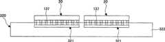
半导体芯片20包括连接焊盘32A和32B以及至少一个连接焊盘32C。连接焊盘32A(电源连接焊盘)通过相应的焊料球137电连接至电路板121的相应内部连接端子136A。连接焊盘32B(接地焊盘)通过相应的焊料球137电连接至电路板121的相应内部连接端子136B。连接焊盘32C为用于信号的电极焊盘(信号电极焊盘),其通过相应的焊料球137电连接至电路板121的相应内部连接端子136C。可采用导电材料(例如Sn-Ag焊料)作为焊料球137的材料。The
电路板121包括多层互连结构122、电容器结构123、绝缘膜132、通路133A至133C、以及内部连接端子136A至136C。可采用例如印刷线路板和陶瓷电路板的衬底作为电路板121。The
多层互连结构122包括多个堆叠的绝缘层138、多条互连线139、通路140、焊盘142、以及外部连接端子144。The
将通路140设置为使其穿过堆叠的绝缘层138。每个通路140的一端连接至相应的焊盘142,另一端连接至相应的外部连接端子144。通路140电连接至互连线139。可采用导电材料(例如Cu和Ni)作为互连线139和通路140的材料。A via 140 is provided so that it passes through the stacked insulating
在位于连接电容器结构123的一侧上的相应通路140端设置焊盘142。每个焊盘142电连接至通路133A至133C中的相应通路。可采用导电材料作为焊盘142的材料。具体地,例如可采用Ni。
在未设置焊盘142的一侧的通路140端设置外部连接端子144。外部连接端子144连接至例如另一未图示的电路衬底。An
电容器结构123在设置焊盘142的一侧粘附至多层互连结构122。电容器结构123位于半导体芯片20之下。电容器结构123覆盖有绝缘膜132。The
电容器结构123包括Si衬底36、绝缘膜45、薄膜电容器46、保护膜125、垂直互连线126和127、以及焊盘电极128和129。The
Si衬底36为薄板,其中形成直径为R2的通孔124。通孔124对应于通路133A至133C的形成位置。将通孔124形成为使其直径R2大于通路133A至133C的直径。薄板Si衬底36的厚度M1小于通孔124的直径R2。The
因此,通过在薄Si衬底36中形成直径R2大于通路133A至133C的直径的通孔124,能够形成孔径比减小的良好通孔124。Therefore, by forming the via
通孔124的直径R2例如可为100μm。在形成通孔124时其节距可设置为例如150μm至250μm。直径R2和通孔124的设置节距并不限于上述数值。The diameter R2 of the through
此外,优选地,Si衬底36的厚度M1在30μm至100μm的范围内。在厚度M1小于30μm的情况下,Si衬底36的强度不足。如果厚度M1大于100μm,通孔124的孔径比(M1/R2)变高,因此难以形成通孔124。Furthermore, preferably, thickness M1 of
通过绝缘膜45在Si衬底36上形成薄膜电容器46。在对应于通孔124的位置形成开口(未图示)。每个薄膜电容器46包括介电膜48、下电极47和上电极49。介电膜48夹在下电极47与上电极49之间。下电极47、介电膜48和上电极49以所述顺序堆叠在绝缘膜45上。A
下电极47、介电膜48和上电极49中的每一个可采用第一实施例中所述的那些材料作为其材料。优选地,介电膜48由具有高介电常数的钙钛矿型晶体结构的金属氧化物材料构成。在采用具有钙钛矿型晶体结构的金属氧化物材料作为介电膜48的情况下,优选采用Pt作为下电极47的材料。采用Pt能够使得介电膜48外延生长,从而增加介电膜48的介电常数。Each of the
每个薄膜电容器46的下电极47通过相应的垂直互连线126和焊盘电极128电连接至相应的内部连接端子136A。每个薄膜电容器46的上电极49通过相应的垂直互连线127和焊盘电极129电连接至相应的内部连接端子136B。每个薄膜电容器46通过相应的内部连接端子136A和136B电连接至半导体芯片20的电源电极焊盘32A和接地电极焊盘32B,以用作去耦电容器。The
在图10中,从右侧开始的第二薄膜电容器46也在前侧或后侧上电连接至内部连接端子136A(未图示),并且最右端的薄膜电容器46也分别在前后侧(或后前侧)上电连接至内部连接端子136A和136B(未图示)。按照本实施例,薄膜电容器46可彼此物理分离或互连。In FIG. 10, the
保护膜125设置于Si衬底36上。将保护膜125形成为覆盖薄膜电容器46并填充通孔124。保护膜125可采用与第一实施例所述的绝缘膜39或保护膜51相同的材料。The
在连接焊盘128下的保护膜125中设置垂直互连线126。垂直互连线126电连接至相应的下电极47和连接焊盘128。在连接焊盘129下的保护膜125中设置垂直互连线127。垂直互连线127电连接至相应的上电极49和连接焊盘129。
焊盘电极128设置在形成于保护膜125中的垂直互连线126上,以电连接至垂直互连线126和内部连接端子136A。焊盘电极129设置在形成于保护膜125中的垂直互连线127上,以电连接至垂直互连线127和内部连接端子136B。The
设置绝缘膜132以填充通孔124并覆盖电容器结构123。绝缘膜132包括暴露相应焊盘142的通孔143。Si衬底36与通路133A至133C中的每一个通路之间的绝缘膜132的厚度L1例如可为0.05μm至50μm。绝缘膜132可采用与第一实施例所述的绝缘材料39的材料相同的材料。An insulating
通路133A形成于与内部连接端子136A的形成位置对应的通孔143中,并电连接至内部连接端子136A和相应的的通路140。通路133B形成于与内部连接端子136B的形成位置对应的通孔143中,并电连接至内部连接端子136B和相应的的通路140。通路133C形成于与内部连接端子136C的形成位置对应的通孔143中,并电连接至内部连接端子136C和相应的的通路140。The
内部连接端子136A设置在与形成于绝缘膜132中的通路133A的形成位置对应的位置处的绝缘膜132上,并电连接至焊盘电极128和通路133A。内部连接端子136A通过相应的焊料球137电连接至半导体芯片20的电源连接焊盘32A。内部连接端子136B设置在与形成于绝缘膜132中的通路133B的形成位置对应的位置处的绝缘膜132上,并电连接至焊盘电极129和通路133B。内部连接端子136B通过相应的焊料球137电连接至半导体芯片20的接地焊盘32B。内部连接端子136C设置在与形成于绝缘膜132中的通路133C的形成位置对应的位置处的绝缘膜132上,并电连接至通路133C。内部连接端子136C通过相应的焊料球137电连接至半导体芯片20的信号连接焊盘32C。The
按照本实施例的半导体器件120,Si衬底36的厚度M1可小于或等于通孔124的直径R2。因此,能够设置具有良好精确度的通孔124,并实现可支持密度进一步增加的半导体器件120。According to the semiconductor device 120 of this embodiment, the thickness M1 of the
此外,由于靠近半导体芯片20设置薄膜电容器46,因此可实现其中等效串联电感降低以及半导体芯片20可以高频运行的半导体器件120。Furthermore, since the
按照本实施例,对薄膜电容器46用作去耦电容器的情况进行说明。但是,薄膜电容器46也可用作除去耦电容器之外的电容器。According to this embodiment, the case where the
图11A至图11J为按照第四实施例的半导体器件制造方法的示意图。以下参照附图说明按照本实施例的半导体器件120的制造方法。11A to 11J are schematic diagrams of a method of manufacturing a semiconductor device according to a fourth embodiment. A method of manufacturing the semiconductor device 120 according to the present embodiment will be described below with reference to the drawings.
首先,在图11A的处理中,通过溅射在其表面上形成有热氧化膜的Si衬底36上形成绝缘膜45。并且,连续形成下电极膜47A、介电膜48A和上电极膜49A,作为薄膜电容器多层体。绝缘膜45用作粘附层。First, in the process of FIG. 11A, an insulating
具体地,例如,使用多靶DC-RF磁控管溅射装置,在Si衬底36上形成非晶氧化铝膜(厚度为50nm)作为绝缘膜45,其中在衬底温度为200℃的情况下,在Si衬底36上形成SiO2膜。接着,在衬底温度为200℃的情况下,形成Pt膜(厚度为100nm)作为下电极膜47A。接着,在衬底温度为600℃的情况下,形成BST膜(厚度为100nm)作为介电膜48A。接着,在衬底温度为25℃的情况下,连续形成IrOx膜和Au膜(厚度为100nm)作为上电极膜49A。这些多层膜45、47A、48A和49A可通过溅射以外的方法(例如气相沉积或CVD)形成。Specifically, for example, an amorphous aluminum oxide film (with a thickness of 50 nm) is formed as the insulating
接下来,在图11B的处理中,通过离子铣削将堆叠的上电极膜49A、介电膜48A和下电极膜47A一起图案化,从而形成包含下电极47、介电膜48和上电极49的每个薄膜电容器46。接着,在氧气氛中热处理薄膜电容器46以去除热变形并将氧原子提供至介电膜48及IrOx膜的缺氧部分。通过分别图案化下电极膜47A、介电膜48A和上电极膜49A,形成每个薄膜电容器46的下电极47、介电膜48和上电极49。Next, in the process of FIG. 11B , the stacked
因而,通过在Si衬底36中形成通孔124之前形成薄膜电容器46,能够高温(300℃-1000℃)形成介电膜48,因此可以形成高介电常数、大电容、及高可靠性的薄膜电容器46。Thus, by forming the
此外,通过在均匀平坦的绝缘膜45上连续堆叠下电极膜47A、介电膜48A和上电极膜49A,并随后图案化下电极膜47A、介电膜48A和上电极膜49A,形成每个薄膜电容器46。因此,能够增加薄膜电容器46的成品率。Furthermore, each formed by successively stacking the
此外,可防止在形成开口部分(孔)145(图11E)、通孔124和143、以及通路133A至133C的过程中所产生的灰尘和杂质粘附于对应于薄膜电容器46的形成区的部分绝缘膜45。因此,能够增加薄膜电容器46的成品率。In addition, dust and impurities generated in the process of forming the opening portion (hole) 145 ( FIG. 11E ), the through
接下来,在图11C所示的处理中,形成保护膜125以覆盖薄膜电容器46及绝缘膜45。此时,在保护膜125中形成暴露相应的下电极47的开口部分(孔)125A、暴露相应的上电极49的开口部分(孔)125B、和暴露绝缘膜45的开口部分(孔)125C。具体说来,例如,通过旋涂方式涂敷光敏聚酰亚胺树脂(厚度为2μm)作为保护膜125。通过曝光光敏聚酰亚胺树脂并将该光敏聚酰亚胺树脂显影,形成开口部分125A至125C。也可以通过旋涂以外的方法(例如喷射或浸渍)形成绝缘膜125。Next, in the process shown in FIG. 11C , a
Si3N4膜、SiO2膜、或氧化铝膜可用作保护膜125。在这种情况下,例如通过利用RF磁控管溅射装置形成保护膜125,然后通过离子铣削形成开口部分125A至125C。然后,在氧气氛中对保护膜进行后退火处理。在这种情况下,保护膜125可通过溅射以外的方法(例如气相沉积或CVD)形成。A Si3 N4 film, a SiO2 film, or an aluminum oxide film can be used as the
接下来,在图11D所示的处理中,同时形成相应的开口部分125A中的垂直互连线126、相应的开口部分125B中的垂直互连线127、以及焊盘电极128和129。具体说来,例如,通过溅射在图11C所示的结构上连续形成作为Ti膜和Cu膜电镀籽晶层。然后,在该电镀籽晶层上形成抗蚀层,以使该抗蚀层具有暴露焊盘电极128和129形成区的开口部分(孔),并通过电镀在该电镀籽晶层上沉积电镀膜。在形成垂直互连线126和127以及焊盘电极128和129之后,去除该抗蚀层。接着,去除其上未形成电镀膜的电镀籽晶层的多余部分。例如,可采用Cu电镀膜作为电镀膜。可通过溅射以外的方法(例如气相沉积或CVD)形成该电镀籽晶层。Next, in the process shown in FIG. 11D , the
接下来,在图11E所示的处理中,从Si衬底36的第一主表面侧蚀刻由开口部分125C暴露的部分绝缘膜45和对应于开口部分125C的部分Si衬底36,从而在Si衬底36中形成直径为R2的开口部分145。开口部分145具有与通孔124基本上相同的深度(垂直尺寸),并当减小Si衬底36的厚度时变为通孔124。例如,可采用湿蚀刻和等离子体蚀刻作为蚀刻方法。可采用氟化氢和硝酸的液体混合物作为湿蚀刻的蚀刻液。Next, in the process shown in FIG. 11E , the part of the insulating
接下来,在图11F所示的处理中,通过粘合带69将支撑衬底70粘附至图11E所示的结构的第一主表面侧,并从第二主表面侧薄化Si衬底36。结果,在Si衬底36的第二主表面上暴露开口部分145,从而形成通孔124。由此,制造在Si衬底36上具有薄膜电容器46的电容器结构123。Next, in the process shown in FIG. 11F , the
具体说来,例如,使用研磨机将Si衬底36薄化至50μm厚。在薄化Si衬底36之后,去除粘合带69。例如,可采用通过紫外线照射降低其粘度的UV带作为粘合带69。例如,可采用研磨或蚀刻薄化Si衬底36。作为研磨方法,可采用抛光(例如磨光和CMP)及切割。作为蚀刻方法,可采用例如湿蚀刻和等离子体蚀刻。Specifically, for example,
因此,通过在从Si衬底36的第一主表面侧形成基本上与通孔124具有相同深度的开口部分145之后薄化Si衬底36直至暴露开口部分145,从而形成通孔124,由此可以降低孔径比(M1/R2)。这使得能够容易地在Si衬底36中形成通孔124,从而能够降低半导体器件120的制造成本。Therefore, the through-
此外,通过使用成本低于ICP的等离子体蚀刻或湿蚀刻形成开口部分145,能够降低半导体器件120的制造成本。In addition, by forming the opening portion 145 using plasma etching or wet etching, which costs less than ICP, the manufacturing cost of the semiconductor device 120 can be reduced.
接下来,在图11G的处理中,电容器结构123粘附至多层互连结构122以使通孔124暴露焊盘142。例如使用环氧基粘合剂将电容器结构123粘附至多层互连结构122。Next, in the process of FIG. 11G ,
接下来,在图11H的处理中,形成绝缘膜132以覆盖电容器结构123并填充通孔124。然后,硬化绝缘膜132。具体说来,例如,通过旋涂方式涂敷环氧树脂(其为耐热树脂)作为绝缘膜132,然后在200℃的温度下热固该环氧树脂。也可以通过旋涂以外的方法(例如喷射或浸渍)涂敷绝缘膜132。此外,也可以使用膜状树脂层作为绝缘膜132。可采用与第一实施例所述的绝缘材料39相同的材料作为绝缘膜132的材料。Next, in the process of FIG. 11H , an insulating
接下来,在图11I的处理中,在绝缘膜132中形成暴露焊盘电极128的开口部分(孔)132A、暴露焊盘电极129的开口部分(孔)132B、以及暴露焊盘142的通孔143。具体说来,通过使用耐热树脂或低k树脂作为绝缘膜132进行ArF受激准分子激光器处理形成开口部分132A、开口部分132B、以及通孔143。也可以使用ArF受激准分子激光器处理以外的激光处理方法、或等离子体蚀刻形成开口部分132A、开口部分132B、以及通孔143。在使用光敏树脂作为绝缘膜132的情况下,可通过曝光并显影对应于开口部分132A、开口部分132B、以及通孔143的部分绝缘膜132形成开口部分132A、开口部分132B、以及通孔143。Next, in the process of FIG. 11I , an opening portion (hole) 132A exposing the
因此,通过使用绝缘材料(例如,低k树脂、耐热树脂、或光敏树脂)填充通孔124,并通过激光通路处理形成用于通路133A至133C的通孔143,可降低制造成本。Therefore, manufacturing cost can be reduced by filling the via
接下来,在图11J的处理中,通过与上述图11D的处理相同的方法,同时形成通路133A至133C以及内部连接端子136A至136C。结果,制造出具有电容器结构123的电路板121。Next, in the process of FIG. 11J , vias 133A to 133C and
因此,通过同时形成通路133A至133C以及内部连接端子136A至136C,能够简化半导体器件120的制造工艺并降低其制造成本。此外,通过在薄化Si衬底36之后形成通路133A至133C,可减小通路133A至133C的深度(垂直尺寸)。因此,能够在连接至内部连接端子136A至136C的半导体芯片20与连接至外部连接端子144的另一电路板(未图示)之间高速传输高频信号。Therefore, by simultaneously forming the
此外,通过减少通孔124的孔径比(M1/R2),能够减少通路133A至133C的形成时间,从而提高生产率。Furthermore, by reducing the aperture ratio (M1/R2) of the through
然后,电路板121的内部连接端子136A至136C分别连接至半导体芯片20的连接焊盘32A至32C。由此制造半导体器件120。Then, the
按照本实施例的半导体器件制造方法,在其上形成薄膜电容器46的一侧的Si衬底36中形成基本上与通孔124具有相同深度的开口部分145,其后,通过减少Si衬底36的厚度直至暴露开口部分145(图11E)形成通孔124。因而,能够减少通孔124的孔径比。这使得能够容易地在Si衬底36中形成通孔124,从而能够降低半导体器件120的制造成本。According to the semiconductor device manufacturing method of this embodiment, the opening portion 145 having substantially the same depth as the through
此外,由于在形成开口部分之前形成薄膜电容器46,能够高温形成每个薄膜电容器46的介电膜48,因此可以形成高介电常数、大电容、及高可靠性的薄膜电容器46。Furthermore, since the
此外,能够防止在通孔124的形成过程中所产生的灰尘和杂质粘附至薄膜电容器。因此,能够增加薄膜电容器46的成品率。In addition, it is possible to prevent dust and impurities generated during the formation of the via
图12A和图12B为按照本发明第四实施例的另一半导体器件制造方法的示意图。12A and 12B are schematic views of another semiconductor device manufacturing method according to the fourth embodiment of the present invention.
在按照本实施例的上述半导体器件制造方法中,薄化Si衬底36之前在Si衬底36中形成开口部分145,其后,薄化Si衬底36直至暴露开口部分145,从而形成通孔124。可选地,如图12A所示,支撑衬底70可通过粘合带69在Si衬底36的上表面36A侧上粘附至图11D所示结构的Si衬底36,并且Si衬底36可从其下表面36B侧薄化(衬底薄化处理)。然后,如图12B所示,可在Si衬底36中形成通孔124(通孔形成处理)。可从Si衬底36的上表面36A侧或下表面36B侧形成通孔124。In the above-described semiconductor device manufacturing method according to the present embodiment, the opening portion 145 is formed in the
评估通过上述图11A至图11J的制造方法所完成的包括电容器结构的电路板的电特性和可靠性。使用图11A至图11J的制造方法中所指定的条件完成该电路板。对于电特性而言,评估结果为电容密度为4μF/cm2、ESR(等效串联电阻)为0.01Ω、ESL(等效串联电感)为10pH、和耐压为20V或以上。这些结果证明能够形成具有电容器结构(其具有大电容及减小的ESL)的电路板。The electrical characteristics and reliability of the circuit board including the capacitor structure completed by the manufacturing method of FIGS. 11A to 11J described above were evaluated. The circuit board was completed using the conditions specified in the manufacturing method of FIGS. 11A to 11J . As for the electrical characteristics, the evaluation results were that the capacitance density was 4 μF/cm2 , the ESR (equivalent series resistance) was 0.01Ω, the ESL (equivalent series inductance) was 10 pH, and the withstand voltage was 20 V or more. These results demonstrate that it is possible to form circuit boards with capacitor structures with large capacitance and reduced ESL.
在温度为121℃、相对湿度为85%、外加电压为3V、和测试时间为48小时的条件下执行高温高湿负荷测试。测试后的绝缘电阻大于或等于10MΩ,这证明具有该电容器结构的电路板在高温高湿条件下也具有足够的可靠性。The high temperature and high humidity load test was performed under the conditions of a temperature of 121° C., a relative humidity of 85%, an applied voltage of 3 V, and a test time of 48 hours. The insulation resistance after the test is greater than or equal to 10MΩ, which proves that the circuit board with this capacitor structure also has sufficient reliability under high temperature and high humidity conditions.
图13为按照本发明第四实施例的第一变化例的半导体器件150的横截面图。图13中,以相同的标号代表与第四实施例的上述半导体器件120的那些元件相同的元件,并省略其说明。FIG. 13 is a cross-sectional view of a semiconductor device 150 according to a first modification of the fourth embodiment of the present invention. In FIG. 13, the same elements as those of the above-described semiconductor device 120 of the fourth embodiment are denoted by the same reference numerals, and descriptions thereof are omitted.
参照图13,半导体器件150包括半导体芯片20和电路板151。除在电路板121上进一步设置电容器结构123、绝缘膜132、绝缘膜152、通路133A至133C、内部连接端子136A至136C、通路153、焊盘154之外,电路板151的结构与电路板121相同。也就是说,电路板151包括两个叠置电容器结构123。Referring to FIG. 13 , a semiconductor device 150 includes a
为便于说明,在以下对设置于电路板151中的两个电容器结构123的说明中,将设置于多层互连结构122上的一个称为电容器结构123-1,将设置于电容器结构123-1上的另一个称为电容器结构123-2。此外,同样的原因,将设置于电容器结构123-1上的绝缘膜132、设置于该绝缘膜132中的通路133A至133C、以及设置于电容器结构123-1上的内部连接端子136A至136C分别称为绝缘膜132-1、通路133A-1至133C-1、以及内部连接端子136A-1至136C-1,而将设置于电容器结构123-2上的绝缘膜132、设置于该绝缘膜132中的通路133A至133C、以及设置于电容器结构123-2上的内部连接端子136A至136C分别称为绝缘膜132-2、通路133A-2至133C-2、以及内部连接端子136A-2至136C-2(图13)。For ease of description, in the following description of the two
设置绝缘膜152以覆盖图10所示的结构(电路板121)的上表面。例如,绝缘膜152可采用与第一实施例所述的绝缘材料39的材料相同的材料。An insulating film 152 is provided to cover the upper surface of the structure (circuit board 121 ) shown in FIG. 10 . For example, the insulating film 152 may use the same material as that of the insulating
在位于内部连接端子136A-1至136C-1与焊盘154之间的绝缘膜152中设置通路153。每个通路153的一端连接至内部连接端子136A-1至136C-1中的相应端子,而另一端连接至相应的焊盘154。可采用导电材料作为通路153的材料。具体地,例如可采用Cu和Ni。可通过例如电镀、气相沉积、CVD或溅射形成通路153。Vias 153 are provided in insulating film 152 between
在对应于通路153的形成位置的位置处的绝缘膜152上设置焊盘154。焊盘154电连接至通路153和通路133A-2至133C-2。The pad 154 is provided on the insulating film 152 at a position corresponding to the formation position of the via 153 . The pad 154 is electrically connected to the via 153 and the
在其上形成有焊盘154的绝缘膜152上设置电容器结构123-2。电容器结构123-2具有与电容器结构123-1相同的结构。设置绝缘膜132-2以覆盖电容器结构123-2。绝缘膜132-2包括暴露垂直互连线126和127及焊盘154的开口部分。通路133A-2至133C-2设置于焊盘154上的绝缘膜132-2中。通路133A-2至133C-2分别电连接至相应的焊盘154和内部连接端子136A-2至136C-2。The capacitor structure 123-2 is provided on the insulating film 152 on which the pad 154 is formed. The capacitor structure 123-2 has the same structure as the capacitor structure 123-1. An insulating film 132-2 is provided to cover the capacitor structure 123-2. The insulating film 132 - 2 includes an opening portion exposing the
内部连接端子136A-2设置在与通路133A-2的形成位置对应的位置处的绝缘膜132-2上。内部连接端子136A-2通过相应的焊料球137电连接至半导体芯片20的电源连接焊盘32A。The
内部连接端子136B-2设置在与通路133B-2的形成位置对应的位置处的绝缘膜132-2上。内部连接端子136B-2通过相应的焊料球137电连接至半导体芯片20的接地焊盘32B。内部连接端子136C-2设置在与通路133C-2的形成位置对应的位置处的绝缘膜132-2上。内部连接端子136C-2通过相应的焊料球137电连接至半导体芯片20的信号连接焊盘32C。The
按照本实施例的第一变化例的半导体器件150,通过在多层互连结构122上堆叠两个电容器结构123-1和123-2,可增加电路板151的薄膜电容器46的电容。此外,按照本实施例的第一变化例的半导体器件150可产生与上述半导体器件120相同的效果。According to the semiconductor device 150 of the first modification of the present embodiment, by stacking the two capacitor structures 123 - 1 and 123 - 2 on the
本实施例的第一变化例的上述说明以具有堆叠于多层互连结构122上的两个电容器结构123-1和123-2为例。可选地,两个以上的电容器结构123可堆叠于多层互连结构122上。此外,可在其上设置有外部连接端子144的多层互连结构122的一侧上设置一个或多个电容器结构123。The above description of the first variation example of this embodiment takes two capacitor structures 123 - 1 and 123 - 2 stacked on the
通过在形成图11J所示的上述结构(电路板121)之后连续形成绝缘膜152和通路153,然后执行与图11G至图11J所示的上述制造方法相同的处理,形成具有上述结构的半导体器件150。A semiconductor device having the above-mentioned structure is formed by successively forming the insulating film 152 and the via 153 after forming the above-mentioned structure (circuit board 121) shown in FIG. 150.
图14为按照本发明第四实施例的第二变化例的半导体器件155的横截面图。图14中,以相同的标号代表与上述第四实施例的半导体器件120的那些元件相同的元件,并省略其说明。此外,在图14中,主要示出设置于电路板156中的多个电容器结构157与半导体器件20之间的位置关系,并省略除电容器结构157之外的电路板156的部件的图示。FIG. 14 is a cross-sectional view of a semiconductor device 155 according to a second modification of the fourth embodiment of the present invention. In FIG. 14, the same elements as those of the semiconductor device 120 of the fourth embodiment described above are denoted by the same reference numerals, and descriptions thereof are omitted. In addition, in FIG. 14 , the positional relationship between the plurality of capacitor structures 157 provided on the circuit board 156 and the
参照图14,半导体器件155包括半导体芯片20和电路板156。除电容器结构157位于半导体器件20之下并靠近半导体器件20之外,电路板156的结构与参照图10所述的电路板121的结构相同。Referring to FIG. 14 , a semiconductor device 155 includes a
电容器结构157位于半导体器件20之下并靠近半导体器件20。为单个半导体芯片20设置多个电容器结构157。每个电容器结构157具有小于半导体芯片20的面积。The capacitor structure 157 is located below and adjacent to the
除面积小于半导体器件20之外,每个电容器结构157具有与电容器结构123相同的结构。此外,尽管未图示,但是形成于电容器结构157中的每个薄膜电容器46电连接至半导体芯片20的相应电源连接焊盘32A和接地焊盘32B,以用作去耦电容器。Each capacitor structure 157 has the same structure as the
按照本实施例的第二变化例的半导体器件155,每个电容器结构157的面积小于半导体芯片20,因此可减小下电极膜47A、介电膜48A以及上电极膜49A的薄膜质量及厚度的变化。因此,能够增加电容器结构157的成品率。此外,按照本实施例的第二变化例的半导体器件155可产生与上述半导体器件120相同的效果。According to the semiconductor device 155 of the second modification example of the present embodiment, the area of each capacitor structure 157 is smaller than that of the
图15为按照本发明第四实施例的第三变化例的半导体器件160的横截面图。在图15中,以相同的标号代表与上述第四实施例的半导体器件120的那些元件相同的元件,并省略其说明。此外,在图15中,主要示出半导体器件20与电容器结构123之间的位置关系,并省略除电容器结构123之外的电路板161的部件的图示。FIG. 15 is a cross-sectional view of a
参照图15,半导体器件160包括半导体芯片20和包含电容器结构123的电路板161。电路板161例如为多芯片模块(MCM)衬底。Referring to FIG. 15 , a
电容器结构123位于相应的半导体芯片20之下并靠近该半导体芯片20。每个电容器结构123的面积基本上与每个半导体芯片20的面积相同。为相应的半导体芯片20设置每个电容器结构123。尽管未图示,但是形成于每个电容器结构123中的每个薄膜电容器46电连接至相应半导体芯片20的相应电源连接焊盘32A和接地焊盘32B,以用作去耦电容器。The
因此,在其上将安装多个半导体芯片20的电路板161中,可与半导体芯片20一一对应地设置多个电容器结构123,每个电容器结构123的面积基本上与每个半导体芯片20的面积相同。Therefore, in the
按照本实施例的第三变化例的半导体器件160可产生与上述半导体器件120相同的效果。此外,取代电容器结构123,可为每个半导体芯片20设置多个电容器结构157(图14)。The
图16为按照本发明第四实施例的第四变化例的半导体器件165的横截面图。在图16中,以相同的标号代表与上述半导体器件120的那些元件相同的元件,并省略其说明。16 is a cross-sectional view of a
参照图16,半导体器件165包括半导体芯片20和其上安装半导体芯片20的电路板170。Referring to FIG. 16, a
除电容器结构175取代电容器结构123之外,电路板170的结构与第四实施例所述的电路板121(图10)相同。The structure of the
除每个均为三层结构的多层薄膜电容器166、垂直互连线171至174、以及焊盘电极176至178分别取代设置在电容器结构123中的薄膜电容器46、垂直互连线126和127、以及焊盘电极128和129之外,电容器结构175的结构与第四实施例所述的电容器结构123相同。The
多层薄膜电容器166设置于覆盖薄化的Si衬底36的绝缘膜45上。每个多层薄膜电容器166位于相应焊盘电极176(其电连接至半导体芯片20的电源连接焊盘32A)与相应焊盘电极177之间(其电连接至半导体芯片20的接地焊盘32B)。多层薄膜电容器166覆盖有保护膜125。按照本变化例,多层薄膜电容器166可彼此物理隔离或互连。The
每个多层薄膜电容器166包括下电极47、第一介电膜48-1、中间电极167-1、第二介电膜48-2、中间电极167-2、第三介电膜48-3和上电极49,它们以所述顺序连续堆叠在绝缘膜45上。设置每个中间电极167-1和167-2以使其夹在介电膜48-1至48-3中的相邻两个介电膜之间。中间电极167-1和167-2可采用与第一实施例所述的下电极47或上电极49相同的材料。中间电极167-1和167-2的厚度例如可为(但不限于)100nm。Each
在对应于通路133A至133C的形成位置的位置处的薄膜电容器166中形成多个开口部分(孔)179。将开口部分179的形状设置为从Si衬底36朝着上电极49变宽。每个开口部分179暴露每个相应的薄膜电容器166的每个下电极47、介电膜48-1、中间电极167-1、介电膜48-2、中间电极167-2、介电膜48-3和上电极49的侧面。A plurality of opening portions (holes) 179 are formed in the
通过在薄膜电容器166中设置这种变宽形状的开口部分179,能够将位于焊盘电极176和177下的电极47、167-1、167-2和49通过垂直互连线171至174电连接至焊盘电极176和177。By providing such a widened-shaped
在对应于焊盘电极176的形成位置的位置处的保护膜125中设置垂直互连线171。垂直互连线171电连接由相应的开口部分179暴露的下电极47和焊盘电极176。在靠近垂直互连线171的位置处的保护膜125中设置垂直互连线172。垂直互连线172电连接由相应的开口部分179暴露的中间电极167-2和焊盘电极176。The
在对应于焊盘电极177的形成位置的位置处的保护膜125中设置垂直互连线173。垂直互连线173电连接由相应的开口部分179暴露的中间电极167-1和焊盘电极177。在靠近垂直互连线173的位置处的保护膜125中设置垂直互连线174。垂直互连线174电连接由相应的开口部分179暴露的上电极49和焊盘电极177。例如可采用导电材料(例如Cu或Ni)作为垂直互连线171至174的材料。The
图17为示出垂直互连线171至174的设置位置的电容器结构175的俯视图。FIG. 17 is a plan view of the
如图17所示,垂直互连线171和垂直互连线172设置于以相应的通孔124的中心轴A1为中心的各同心圆上,而垂直互连线173和垂直互连线174设置于以相应的通孔124的中心轴A2为中心的各同心圆上。As shown in FIG. 17, the
垂直互连线171至174可采用与第四实施例所述的垂直互连线126和127的材料相同的材料。垂直互连线171至174的形状可为(但不限于)如图17所示的圆柱形。例如,垂直互连线171至174也可为四棱柱形。The
焊盘电极176设置于对应于垂直互连线171和172的形成位置的位置处的保护膜125上,以包围相应的通孔124。焊盘电极176电连接至垂直互连线171和172以及内部连接端子136A。焊盘电极176通过垂直互连线171和172电连接至每个相应薄膜电容器166的叠置电极47、167-1、167-2、和49中从Si衬底36侧计数的奇数电极,即第一电极47和第三电极167-2。此外,焊盘电极176通过内部连接端子136A电连接至半导体芯片20的电源连接焊盘32A。
焊盘电极177设置于对应于垂直互连线173和174的形成位置的位置处的保护膜125上,以包围相应的通孔124。焊盘电极177电连接至垂直互连线173和174以及内部连接端子136B。焊盘电极177通过垂直互连线173和174电连接至每个相应的薄膜电容器166的叠置电极47、167-1、167-2、和49中从Si衬底36侧计数的偶数电极,即第二电极167-1和第四电极49。此外,焊盘电极177通过内部连接端子136B电连接至半导体芯片20的接地焊盘32B。
通过如此电连接焊盘电极176与从Si衬底36侧计数的奇数电极47和167-2以及电连接焊盘电极177与从Si衬底36侧计数的偶数电极167-1和49,并联连接每个多层薄膜电容器166中设置的多个电容器,从而使每个多层薄膜电容器166用作去耦电容器。By thus electrically connecting the
焊盘电极178设置于保护膜125中未形成垂直互连线171至174的部分上,以包围相应的通孔124。焊盘电极178电连接半导体芯片20的信号连接焊盘32C。可采用与第四实施例所述的焊盘电极128和129相同的材料作为焊盘电极176至178的材料。
按照本实施例的第四变化例的半导体器件165,设置于每个多层薄膜电容器166中的多个电容器并联连接。因此,能够增加电容器电容。According to the
本实施例的第四变化例的上述说明以三层结构的多层薄膜电容器166为例。可选地,电容器的叠层数目可为两个或大于三个。可以与图11A至图11F所示的上述方法相同的方法制造电容器结构175。The above description of the fourth variation example of this embodiment takes the
【第五实施例】[fifth embodiment]
图18为传统多层薄膜电容器520的横截面图。FIG. 18 is a cross-sectional view of a conventional multilayer film capacitor 520 .
参照图18说明传统的多层薄膜电容器520。多层薄膜电容器520覆盖有光敏聚酰亚胺529。多层薄膜电容器520包括Si衬底521、SrTiO3层522、下电极524、介电膜525、中间电极526、介电膜527、上电极528、焊盘电极531至533、以及端子534至536。SrTiO3层522为中间层。以下述顺序在Si衬底521上连续堆叠SrTiO3层522、下电极524、介电膜525、中间电极526、介电膜527和上电极528。A conventional multilayer film capacitor 520 will be described with reference to FIG. 18 . The multilayer film capacitor 520 is covered with photosensitive polyimide 529 . A multilayer film capacitor 520 includes a Si substrate 521, a SrTiOlayer 522, a lower electrode 524, a dielectric film 525, an intermediate electrode 526, a dielectric film 527, an upper electrode 528, pad electrodes 531 to 533, and terminals 534 to 536 . The SrTiO3 layer 522 is an intermediate layer. A SrTiO3 layer 522, a lower electrode 524, a dielectric film 525, an intermediate electrode 526, a dielectric film 527, and an upper electrode 528 are successively stacked on a Si substrate 521 in the following order.
焊盘电极531连接至上电极528。焊盘电极532连接至中间电极526。焊盘电极533连接至下电极524。从而形成由上电极528、介电膜527和中间电极526构成的电容器B1和由下电极524、介电膜525和中间电极526构成的电容器B2。电容器B1与电容器B2的电容不同。The pad electrode 531 is connected to the upper electrode 528 . The pad electrode 532 is connected to the intermediate electrode 526 . The pad electrode 533 is connected to the lower electrode 524 . Thus, a capacitor B1 composed of the upper electrode 528, the dielectric film 527, and the intermediate electrode 526, and a capacitor B2 composed of the lower electrode 524, the dielectric film 525, and the intermediate electrode 526 are formed. Capacitor B1 and capacitor B2 have different capacitances.
端子534设置于焊盘电极531上。端子535设置于焊盘电极532上。端子536设置于焊盘电极533上。端子534至536中的每个端子连接至未图示的半导体芯片的电源连接焊盘和接地焊盘中的相应焊盘。The terminal 534 is provided on the pad electrode 531 . The terminal 535 is provided on the pad electrode 532 . The terminal 536 is provided on the pad electrode 533 . Each of the terminals 534 to 536 is connected to a corresponding one of power connection pads and ground pads of the unillustrated semiconductor chip.
图19为示出在并联连接相同电容的两个电容器的情况下等效电路的电路图。作为实例,图19示出高频半导体芯片的电源连接焊盘和接地焊盘之间并联连接两个电容器B2的情况。此外,在图19中,P1代表端子534a、534b、535a、535b、536a和536b设置的节距。以下将该节距称为“端子节距P1”.FIG. 19 is a circuit diagram showing an equivalent circuit in a case where two capacitors of the same capacitance are connected in parallel. As an example, FIG. 19 shows a case where two capacitors B2 are connected in parallel between the power connection pad and the ground pad of the high-frequency semiconductor chip. In addition, in FIG. 19, P1 represents the pitch at which the terminals 534a, 534b, 535a, 535b, 536a, and 536b are arranged. Hereinafter, this pitch is referred to as "terminal pitch P1".
在采用多层薄膜电容器520作为去耦电容器的情况下,在高频半导体芯片的电源连接焊盘与接地焊盘之间并联连接相同电容的多个电容器,以增加多层薄膜电容器520的电容,从而能够充分吸收高频半导体芯片的噪声。In the case of adopting the multilayer film capacitor 520 as the decoupling capacitor, a plurality of capacitors of the same capacitance are connected in parallel between the power connection pad and the ground pad of the high-frequency semiconductor chip to increase the capacitance of the multilayer film capacitor 520, Thereby, the noise of the high-frequency semiconductor chip can be sufficiently absorbed.
在这种情况下,如图19所示,为了并联连接相同电容的电容器B2,需要互连线L2(用于电连接至高频半导体芯片的电源连接焊盘)和互连线L3(用于电连接至高频半导体芯片的接地焊盘)。此外,在这种情况下,需要每条互连线L2和L3的长度为端子节距P1的三倍。In this case, as shown in FIG. 19, in order to connect capacitors B2 of the same capacity in parallel, an interconnection line L2 (for electrically connecting to the power connection pad of the high-frequency semiconductor chip) and an interconnection line L3 (for electrically connected to the ground pad of the high-frequency semiconductor chip). Also, in this case, the length of each of the interconnection lines L2 and L3 is required to be three times the terminal pitch P1.
因而,在多层薄膜电容器520中,在通过并联连接相同电容的电容器来配置去耦电容器的情况下,每条互连线L2和L3的长度为端子节距P1的三倍。这导致电感增加而不能减少阻抗的问题。尽管未图示,但是在并联连接相同电容的两个电容器B1的情况下,也需要互连线L2和L3,从而导致相同的问题。Thus, in the multilayer film capacitor 520, in the case where a decoupling capacitor is configured by connecting capacitors of the same capacity in parallel, the length of each of the interconnection lines L2 and L3 is three times the terminal pitch P1. This causes a problem that the inductance increases without reducing the impedance. Although not shown, in the case of connecting two capacitors B1 of the same capacitance in parallel, interconnection lines L2 and L3 are also required, resulting in the same problem.
图20为按照本发明第五实施例的电容器结构180的横截面图。在图20中,以相同的标号代表与第四实施例的第四变化例的电容器结构175的那些元件相同的元件,并省略其说明。FIG. 20 is a cross-sectional view of a
参照图20,电容器结构180包括Si衬底181、绝缘膜45、绝缘膜184、薄膜电容器182、保护膜183、垂直互连线185至187、一对焊盘电极189和190、和外部连接端子192和193。Referring to FIG. 20, a
衬底181可采用廉价且平滑度和耐热性极佳的材料。例如,Si为适合于衬底181的材料。其它用于衬底181的材料例如可以为陶瓷(例如玻璃和氧化铝)、金属(例如Mo和W)、树脂(例如环氧树脂)、以及这些材料中的两种或更多种的合成材料。厚度为100nm的SiO2膜可用作绝缘膜45。The
薄膜电容器182设置于绝缘膜45上。薄膜电容器182位于焊盘电极189与焊盘电极190之间,以电连接至与外部连接端子192连接的焊盘电极189和电连接至与外部连接端子193连接的焊盘电极190。The
通过如此设置电连接至一对焊盘电极189和190之间的外部连接端子192和193的薄膜电容器182,相比传统的多层薄膜电容器520,能够减小薄膜电容器182的面积尺寸。By thus providing
薄膜电容器182为多层薄膜电容器,其中下电极47、第一介电膜48-1、中间电极167、第二介电膜48-2和上电极49以所述顺序连续堆叠。在焊盘电极189下的包括薄膜电容器182的薄膜电容器多层体中形成开口部分(孔)196,并在焊盘电极190下的包括薄膜电容器182的薄膜电容器多层体中形成开口部分(孔)197。开口部分196暴露下电极47的上表面并限定中间电极167和上电极49中的每个电极的端面。开口部分197暴露中间电极167的上表面并限定上电极49的端面。此外,开口部分196和197的形状基本上类似于倒截锥形,在从焊盘电极189和190的底表面至衬底181的方向逐渐缩减。也就是说,在开口部分196和197中,电极的端面的相对侧之间的距离(或开口的直径)在从焊盘电极189和190的底表面至衬底181的方向逐渐减小。换句话说,每个开口部分196和197垂直于其轴的横截面面积在从焊盘电极189和190的底表面至衬底181的方向减小。The
通过在薄膜电容器182中设置这种形状的开口部分196和197,能够通过垂直互连线185至187连接焊盘电极189、190与电极47、167和49。在图20中,每个开口部分196和197的形状基本上为倒截锥形。可选地,开口部分196和197的形状基本上可为倒截棱锥形(pyramid-like)。By providing the opening
薄膜电容器182包括由下电极47、第一介电膜48-1和中间电极167构成的电容器D1以及由中间电极167、第二介电膜48-2和上电极49构成的电容器D2。
例如,薄膜电容器182通过未图示的电路板连接至半导体芯片。在这种情况下,薄膜电容器182通过外部连接端子192和193电连接至半导体芯片的电源连接焊盘和接地焊盘,以用作去耦电容器。For example, the
第一实施例所述的具有高介电常数的钙钛矿型晶体结构的金属氧化物材料是作为介电膜48-1和48-2的最理想材料。除第一实施例所述的材料之外,也可以使用Ta、Nb、Hf、Y和Al的金属氧化物,合成氧化物,以及这些氧化物的混合物。关于这些材料的晶体结构,对性质和成本而言,理想地,这些材料为多晶体。可选地,也可以使用昂贵且具有高介电常数的单晶体、具有极佳泄漏特性的非晶体、以及具有这些材料的混合相的晶体。The metal oxide material having a perovskite crystal structure with a high dielectric constant described in the first embodiment is the most ideal material for the dielectric films 48-1 and 48-2. In addition to the materials described in the first embodiment, metal oxides of Ta, Nb, Hf, Y, and Al, synthetic oxides, and mixtures of these oxides can also be used. With regard to the crystal structure of these materials, ideally, these materials are polycrystalline in terms of properties and cost. Alternatively, single crystals that are expensive and have a high dielectric constant, amorphous materials that have excellent leakage characteristics, and crystals that have mixed phases of these materials can also be used.
作为下电极47、中间电极167和上电极49的材料,除第一实施例所述的下电极47和上电极49的材料之外,可使用贵金属(例如Ir、Ru、和Rh)、导电氧化物(例如SrRuO3、LaNiO3、和LaSrCoO3)和导电氮化物(例如AlTiN)。此外,由于贵金属不易于氧化且电阻低,例如Pt(上面描述的)、Ir、Ru和Rh等材料较适用。As materials for the
保护膜183的厚度例如为50nm,并设置为覆盖薄膜电容器182。保护膜183由绝缘材料构成。该绝缘材料不受特殊限制,但优选具有极佳耐湿性的Si3N4、SiO2或氧化铝。采用这些材料能够防止具有钙钛矿型晶体结构的介电膜48-1和48-2的特性退化。The
设置厚度例如为2μm的绝缘膜184,以覆盖保护膜183。在绝缘膜184中形成对应于垂直互连线185的形成位置的开口部分(孔)184A、对应于垂直互连线187的形成位置的开口部分(孔)184B、和对应于垂直互连线186的形成位置的开口部分(孔)184C。开口部分184A暴露部分下电极47。开口部分184B暴露部分中间电极167。开口部分184C暴露部分上电极49。An insulating
可采用与第一实施例所述的绝缘膜52相同的材料作为绝缘膜184的材料。例如,可采用树脂(例如聚酰亚胺树脂和环氧树脂)、氧化物(例如氧化铝和二氧化硅)、氮化物、各种绝缘材料、混合物以及多层膜。As the material of the insulating
垂直互连线185设置于绝缘膜184中以从焊盘电极189的底表面延伸至暴露于开口部分196中的下电极47的上表面。垂直互连线185电连接至焊盘电极189和下电极47。垂直互连线186设置于绝缘膜184中以从焊盘电极189的底表面延伸至上电极49的上表面。垂直互连线186电连接至焊盘电极189和上电极49。垂直互连线187设置于绝缘膜184中以从焊盘电极190的底表面延伸至中间电极167的上表面。垂直互连线187电连接至焊盘电极190和中间电极167。The
图21为示出垂直互连线185至187的设置位置的电容器结构180的俯视图。FIG. 21 is a top view of the
如图21所示,多条(图21中为4个)垂直互连线186设置于以垂直互连线185的中心轴E为中心的圆上,以使该圆与垂直互连线185同心。在图21中,垂直互连线185至187为圆柱形。但是,垂直互连线185至187不限于该形状,也可以为四棱柱形。作为垂直互连线185至187的材料,可采用导电材料,例如Cu和Ni。As shown in FIG. 21 , a plurality of (four in FIG. 21 )
焊盘电极189设置于对应于垂直互连线185和186的形成位置的位置处的绝缘膜184上。焊盘电极189电连接至电极47、167、和49中从Si衬底181侧计数的奇数电极,即第一电极47和第三电极49。The
焊盘电极190设置于对应于垂直互连线187的形成位置的位置处的绝缘膜184上。焊盘电极190电连接至从Si衬底181侧计数的偶数(第二)电极167。如果未设置外部连接端子192和193,焊盘电极189和190可用作替代外部连接端子192和193的端子。The
在位于一对焊盘电极189和190之间的薄膜电容器182的电极47、167、和49中,从Si衬底181侧计数的奇数电极47和49分别通过垂直互连线185和186电连接至焊盘电极189,而从Si衬底181侧计数的偶数电极167通过垂直互连线187电连接至焊盘电极190。因此,能够使电容器D1和D2基本上具有相等的电容。Of the
在图21中,焊盘电极189和190为圆形。但是,焊盘电极189和190不限于该形状,也可以为四边形。作为焊盘电极189和190的材料,例如可采用导电材料,比如Cu和Ni。In FIG. 21, the
外部连接端子192设置于焊盘电极189上。外部连接端子193设置于焊盘电极190上。在外部连接端子192和193中,举例说来,一个电连接至接半导体芯片的电源连接焊盘,另一个电连接至半导体芯片的接地焊盘。作为外部连接端子192和193的材料,可采用导电材料。具体地,例如可采用Sn-Ag焊料。The
图22为示出在并联连接相同电容的两个电容器的情况下等效电路的电路图。在图22中,P2代表外部连接端子192和193设置的节距。FIG. 22 is a circuit diagram showing an equivalent circuit in a case where two capacitors of the same capacitance are connected in parallel. In FIG. 22, P2 represents the pitch at which the
如图22所示,在通过并联连接相同电容的两个电容器D1和D2来配置去耦电容器的情况下,在电容器结构180中通过垂直互连线185至187电连接电极47、167和49以及焊盘电极189和190。因此,电容器结构180中不需要传统薄膜电容器520(图18)所需的互连线L2和L3。结果,在并联连接电容器D1和D2(使用薄膜电容器182作为去耦电容器)的情况下所需的互连线的长度减小,从而降低互连线的电感。因而,能够实现低阻抗的薄膜电容器182。As shown in FIG. 22, in the case of configuring a decoupling capacitor by connecting two capacitors D1 and D2 of the same capacitance in parallel, the
按照本实施例的电容器结构180,焊盘电极189电连接至从Si衬底181侧计数的奇数电极47和49,而焊盘电极190电连接至从Si衬底181侧计数的偶数电极167。结果,并联连接位于焊盘电极189和190之间的基本上具有相同电容的多个电容器D1和D2。因而,能够通过减少在配置去耦电容器的情况下所需的互连线长度,从而降低电感,由此降低阻抗。此外,通过设置电连接至一对焊盘电极189和190之间的两外部连接端子192和193的薄膜电容器182,能够减小薄膜电容器的尺寸。According to
在本实施例的电容器结构180中,薄膜电容器182具有两层结构的电容器D1和D2。可选地,可通过以三层或更多层堆叠电容器来配置薄膜电容器182。通过在电容器结构180中设置通过三层或更多层堆叠电容器而配置的薄膜电容器,并且并联连接基本上具有相同电容的多个电容器,能够进一步增加薄膜电容器的电容。In the
图23A至图23I为按照本发明第五实施例的电容器结构制造方法的示意图。以下参照附图说明按照本实施例的电容器结构180的制造方法。23A to 23I are schematic diagrams of a method for manufacturing a capacitor structure according to a fifth embodiment of the present invention. A method of manufacturing the
首先,在图23A的处理中,通过溅射在Si衬底181上形成绝缘膜45,然后连续形成下电极膜47A、介电膜48-1A、中间电极膜167A、介电膜48-2A和上电极膜49A作为薄膜电容器多层体。First, in the process of FIG. 23A, the insulating
具体地,例如,使用多靶DC-RF磁控管溅射装置,在衬底温度为200℃的情况下在具有(111)主表面的Si衬底181上形成SiO2膜(厚度为100nm)作为绝缘膜4。接着,在衬底温度为600℃的情况下,在Ar气氛中形成作为Pt膜(厚度为100nm)下电极膜47A。接着,在衬底温度为600℃的情况下,在Ar/O2气氛中形成BST膜(厚度为100nm)作为第一介电膜48-1A。接着,在衬底温度为300℃的情况下,在Ar气氛中形成Pt膜(厚度为100nm)作为中间电极膜167A。接着,形成BST膜(厚度为100nm)作为第二介电膜48-2A。接着,形成Pt膜(厚度为100nm)作为上电极膜49A。在形成第二介电膜48-2A的过程中,可采用与第一介电膜48-1A相同的膜形成条件。在形成上电极膜49A的过程中,可采用与中间电极膜167A相同的膜形成条件。这些多层膜45、47A、48-1A、167A、48-2A和49A可通过溅射以外的方法(例如气相沉积或CVD)形成。Specifically, for example, aSiO2 film (with a thickness of 100 nm) was formed on a
接下来,在图23B所示的处理中,通过离子铣削来图案化叠置的膜47A、48-1A、167A、48-2A和49A,从而形成包括下电极47、两层介电膜48-1和48-2、中间电极167和上电极49的薄膜电容器182。通过所述图案化处理在包括薄膜电容器182的薄膜电容器多层体中形成开口部分196和197。Next, in the process shown in FIG. 23B, the
具体说来,形成具有对应于开口部分196和197的形成位置的开口的抗蚀膜,并通过与Si衬底181呈某一角度注入离子进行离子铣削来形成开口部分196和197。Specifically, a resist film having openings corresponding to the formation positions of the opening
接着,在氧气氛中热处理薄膜电容器182以消除介电膜48-1和48-2的热变形并将氧原子提供至介电膜48-1和48-2的缺氧部分。通过分别图案化下电极膜47A、中间电极膜167A和上电极膜49A,形成薄膜电容器182的下电极47、中间电极167和上电极49。Next,
通过在真空中顺序堆叠下电极膜47A、介电膜48-1A、中间膜167A、介电膜48-2A和上电极膜49A,能够防止灰尘或杂质粘附至叠置的膜47A、48-1A、167A、48-2A和49A,从而防止污染每层膜47A、48-1A、167A、48-2A和49A的表面。By sequentially stacking the
此外,通过在均匀平坦的绝缘膜45上形成叠置的膜47A、48-1A、167A、48-2A和49A之后执行图案化,能够以良好的精确度处理叠置的膜47A、48-1A、167A、48-2A和49A,从而能够增加薄膜电容器182的成品率。Furthermore, by performing patterning after forming the
此外,通过使用单个掩模一起图案化叠置的膜47A、48-1A、167A、48-2A和49A,与使用制备的多个掩模执行图案化的情况相比,能够降低电容器结构180的制造成本。In addition, by patterning the
接下来,在图23C所示的处理中,形成保护膜183以覆盖薄膜电容器182。接着,在分别对应于垂直互连线185、187和186的形成位置的位置处,通过离子铣削在保护膜183中形成暴露下电极47的开口183A、暴露中间电极167的开口183B、和暴露上电极49的上表面的开口183C。接着,在氧气氛中对保护膜183进行后退火。具体说来,例如,通过利用RF磁控管溅射装置进行溅射来形成非晶氧化铝膜(厚度为50nm)作为保护膜183。保护膜183可通过溅射以外的方法(例如气相沉积或CVD)形成。Next, in a process shown in FIG. 23C , a
接下来,在图23D的处理中,形成绝缘膜184以覆盖图23C所示的结构的上表面侧。接着,在绝缘膜184中形成开口184A至184C。具体说来,例如,通过旋涂方式形成光敏聚酰亚胺树脂(厚度为2μm)作为绝缘膜184。通过曝光并显影该光敏聚酰亚胺树脂,形成开口部分184A、184B和184C。也可以通过旋涂以外的方法(例如喷射或浸渍)形成绝缘膜184。Next, in the process of FIG. 23D , an insulating
接下来,在图23E所示的处理中,在绝缘膜184的上表面和开口部分184A至184C上形成作为电镀籽晶层的金属膜199。具体说来,例如,通过溅射连续形成Ti膜、Cu膜和Ni膜,以用作金属膜199。金属膜199可通过溅射以外的方法(例如气相沉积或CVD)形成。Next, in a process shown in FIG. 23E , a
接下来,在图23F的处理中,在金属膜199上形成抗蚀层201,该抗蚀层201具有对应于焊盘电极189的形成位置的开口部分(孔)201A以及对应于焊盘电极190的形成位置的开口部分(孔)201B。Next, in the process of FIG. 23F , a resist
接着,在图23G的处理中,在开口部分184A至184C中分别形成垂直互连线185至187。接着,在暴露于抗蚀层201的开口部分201A中的区域内形成焊盘电极189,在暴露于抗蚀层201的开口部分201B中的区域内形成焊盘电极190。具体说来,通过电镀在对应于开口部分184A至184C的部分金属膜199上沉积Cu膜作为垂直互连线185至187,然后,通过电镀形成作为焊盘电极189和190的Ni膜。Next, in the process of FIG. 23G ,
接着,在图23H的处理中,在焊盘电极189和190上形成Sn-Ag焊料的导电材料205。接着,去除抗蚀层201。导电材料205随后回流以作为外部连接端子192和193。Next, in the process of FIG. 23H , a conductive material 205 of Sn—Ag solder is formed on the
接下来,在图23I所示的处理中,去除未被焊盘电极189和190覆盖的金属膜199的多余部分。接着,通过加热使导电材料205回流,从而形成外部连接端子192和193。然后,通过切片方式切割Si衬底181,从而形成电容器结构180。Next, in the process shown in FIG. 23I , excess portions of the
按照本实施例的电容器结构制造方法,薄膜电容器182形成于一对焊盘电极189与焊盘电极190之间,并且在薄膜电容器182的多个电极47、167、和49中,从Si衬底181侧计数的奇数电极47和49通过垂直互连线185和186电连接至焊盘电极189,而从Si衬底181侧计数的偶数电极167通过垂直互连线187电连接至焊盘电极190。因此,能够通过减少在并联连接基本上相同电容的电容器D1和D2(使用薄膜电容器182作为去耦电容器)时所需的互连线长度来降低互连线的电感,从而降低阻抗。According to the capacitor structure manufacturing method of this embodiment, the
此外,通过在真空中顺序堆叠下电极膜47A、介电膜48-1A、中间膜167A、介电膜48-2A和上电极膜49A,能够防止灰尘或杂质粘附至叠置的膜47A、48-1A、167A、48-2A和49A,从而防止污染每层膜47A、48-1A、167A、48-2A和49A的表面。因而,能够增加薄膜电容器182的成品率。Furthermore, by sequentially stacking the
此外,通过在均匀平坦的绝缘膜45上形成叠置的膜47A、48-1A、167A、48-2A和49A之后执行图案化,能够增加薄膜电容器182的成品率。Furthermore, by performing patterning after forming the
此外,通过使用单个掩模一起图案化叠置的膜47A、48-1A、167A、48-2A和49A,与使用为每层膜47A、48-1A、167A、48-2A和49A都制备掩模来执行图案化的情况相比,能够降低电容器结构180的制造成本。Furthermore, by patterning the
制备通过与按照本实施例的上述图23A和图23B的方法相同的方法形成的下电极47、介电膜48-1、中间电极167、介电膜48-2、中间电极167、介电膜48-3和上电极49的三层结构的薄膜电容器(一个实例),并且制备通过每次形成每层膜47、48-1、167、48-2、167、48-3和49时执行图案化所形成的三层结构的传统薄膜电容器(比较例),并对该实例与比较例的电特性进行评估。利用图23A和23B的处理中所指定的条件形成该实例薄膜电容器。The
对于实例薄膜电容器而言,评估结果为电容密度为12μF/cm2、ESR(等效串联电阻)为0.02Ω、ESL(等效串联电感)为10pH、和耐压为30V或以上。对于比较例薄膜电容器而言,评估结果为电容密度为12uF/cm2、ESR(等效串联电阻)为0.02Ω、ESL(等效串联电感)为10pH、和耐压为20V或以下。For the example film capacitor, the evaluation results were a capacitance density of 12 μF/cm2 , an ESR (equivalent series resistance) of 0.02Ω, an ESL (equivalent series inductance) of 10 pH, and a withstand voltage of 30 V or more. For the comparative film capacitor, the evaluation results were that the capacitance density was 12 uF/cm2 , the ESR (equivalent series resistance) was 0.02Ω, the ESL (equivalent series inductance) was 10 pH, and the withstand voltage was 20 V or less.
这些结果证明按照本实施例能够形成具有大电容、减小的ESL、以及极佳耐压特性的薄膜电容器。These results demonstrate that film capacitors having large capacitance, reduced ESL, and excellent withstand voltage characteristics can be formed according to the present example.
此外,制备通过按照本实施例的上述图23A和图23B的处理相同的方法形成的下电极47、介电膜48和上电极49的单层结构的薄膜电容器(一个实例),并且制备通过每次形成每层膜47、48和49时执行图案化所形成的单层结构的传统薄膜电容器(比较例),并对具有10V或以上耐压的两种类型的薄膜电容器(该实例与比较例)的缺陷率进行评估。利用图23A和23B的处理中所指定的条件形成该实例薄膜电容器。In addition, a film capacitor (one example) of a single-layer structure of the
图24为示出每种类型的薄膜电容器的电极面积与缺陷率之间的关系的图表。图24中的上电极面积指上电极49与介电膜48的接触面积。FIG. 24 is a graph showing the relationship between the electrode area and the defect rate of each type of film capacitor. The upper electrode area in FIG. 24 refers to the contact area between the
如图24所示,随着上电极49的面积增加,比较例薄膜电容器的缺陷率急剧增加。另一方面,随着上电极49的面积增加,实例薄膜电容器的缺陷率几乎不增加。具体说来,例如,当上电极49的面积为1cm2时,比较例的成品率为32%(缺陷率为68%),而实例的成品率为92%(缺陷率为8%)。As shown in FIG. 24, as the area of the
这些结果证明与比较例薄膜电容器相比,该实例薄膜电容器可具有更高的成品率。此外,由于上述结果是对于按照本实施例的单层薄膜电容器而获得的,可以预见对于通过相同方法形成的多层薄膜电容器而言,成品率的差距将更显著。These results demonstrate that the film capacitor of this example can have a higher yield than the film capacitor of the comparative example. Furthermore, since the above results were obtained for the single-layer film capacitor according to this embodiment, it is expected that the difference in yield will be more significant for the multilayer film capacitor formed by the same method.
图25为按照本发明第五实施例的第一变化例的电容器结构210的横截面图。在图25中,以相同的标号代表与按照第五实施例的电容器结构180(图20)的那些元件相同的元件,并省略其说明。FIG. 25 is a cross-sectional view of a
参照图25,除三层结构的薄膜电容器211替代设置于上述电容器结构180中的薄膜电容器182以及进一步设置垂直互连线212之外,电容器结构210具有与第五实施例的电容器结构180相同的结构。Referring to FIG. 25, except that a
薄膜电容器211包括下电极47、第一介电膜48-1、中间电极167-1、第二介电膜48-2、中间电极167-2、第三介电膜48-3和上电极49,它们以所述顺序连续堆叠。The
在焊盘电极189下的包括薄膜电容器211的薄膜电容器多层体中形成开口部分(孔)215和216。开口部分215暴露下电极47的上表面并限定中间电极167-1和167-2中的每个电极的端面。开口部分216暴露中间电极167-2的上表面并限定上电极49的端面。Opening portions (holes) 215 and 216 are formed in the thin film capacitor multilayer body including the
开口部分215的形状基本上类似为倒截锥形,在从焊盘电极189的底表面至衬底181的方向逐渐减缩。也就是说,在开口部分215中,电极的端面的相对侧之间的距离(或开口的直径)在从焊盘电极189的底表面至衬底181的方向逐渐减小。换句话说,开口部分215垂直于其轴的横截面面积在从焊盘电极189的底表面至衬底181的方向减小。The shape of the
开口部分216的形状基本上类似为倒截锥形,在从焊盘电极189的底表面至衬底181的方向逐渐减缩。也就是说,在开口部分216中,电极的端面的相对侧之间的距离(或开口的直径)在从焊盘电极189的底表面至衬底181的方向逐渐减小。换句话说,开口部分216垂直于其轴的横截面面积在从焊盘电极189的底表面至衬底181的方向减小。The shape of the
在焊盘电极190下的包括薄膜电容器211的薄膜电容器多层体中形成开口部分(孔)217。开口部分217暴露中间电极167-1的上表面并限定中间电极167-2和上电极49中的每个电极的端面。开口部分217的形状基本上类似为倒截锥形,在从焊盘电极190的底表面至衬底181的方向逐渐减缩。也就是说,在开口部分217中,电极的端面的相对侧之间的距离(或开口的直径)在从焊盘电极190的底表面至衬底181的方向逐渐减小。换句话说,开口部分217垂直于其轴的横截面面积在从焊盘电极190的底表面至衬底181的方向减小。An opening portion (hole) 217 is formed in the thin film capacitor multilayer body including the
通过在包含薄膜电容器211的薄膜电容器多层体中设置这种形状的开口部分215至217,能够通过垂直互连线185至187及212连接焊盘电极189、190与电极47、167-1、167-2和49。在图25中,开口部分215至217均具有基本上类似倒截锥形的形状。可选地,开口部分215至217可基本上具有倒截棱锥形的形状。可通过与图23B的方法相同的方法形成开口部分215至217。By providing the
图26为示出垂直互连线185至187及212的设置位置的示意图。FIG. 26 is a schematic diagram showing the arrangement positions of the
参照图25和图26,垂直互连线185设置于绝缘膜184中以电连接下电极47和焊盘电极189。多条垂直互连线186设置于绝缘膜184中以电连接中间电极167-2和焊盘电极189。垂直互连线186位于以垂直互连线185的中心轴为中心的圆上,以使该圆与垂直互连线185同心。垂直互连线187设置于绝缘膜184中以电连接中间电极167-1和焊盘电极190。垂直互连线212设置于绝缘膜184中以从焊盘电极190的底表面延伸至上电极49的上表面。垂直互连线212电连接上电极49和焊盘电极190。垂直互连线212位于以垂直互连线187的中心轴为中心的圆上,以使该圆与垂直互连线187同心。Referring to FIGS. 25 and 26 , a
焊盘电极189通过垂直互连线185和186电连接至电极47、167-1、167-2和49中从衬底181侧计数的奇数电极,即第一电极47和第三电极167-2。The
焊盘电极190通过垂直互连线187和212电连接至电极47、167-1、、167-2和49中从衬底181侧计数的偶数电极,即第二电极167-1和第四电极49。The
具有这样三层结构的薄膜电容器211的电容器结构210也可产生与按照第五实施例的电容器结构180相同的效果。此外,具有四层或更多层结构的薄膜电容器的电容器结构也可产生与按照第五实施例的电容器结构180相同的效果。可通过与上述图23A至23I的方法相同的方法制造电容器结构210。The
在图26中,每条垂直互连线212为圆柱形。但是,垂直互连线212不限于该形状,也可以为四棱柱形。作为垂直互连线212的材料,可采用与垂直互连线185至187相同的材料。In FIG. 26, each
图27为按照本发明第五实施例的第二变化例的电容器结构220的横截面图。在图27中,以相同的标号代表与按照第五实施例的电容器结构180(图20)的那些元件相同的元件,并省略其说明。FIG. 27 is a cross-sectional view of a
参照图27,电容器结构220的配置方式与上述电容器结构180基本相同,不同之处在于:为构成薄膜电容器182的电极47、49和167以及两层介电膜48-1和48-2分别制备相应的掩模,并当每次形成每层膜47A、48-1A、167A、48-2A和49A时通过该相应的掩模执行图案化。Referring to FIG. 27 , the configuration of the
作为如此制备多个掩模并当每次形成每层膜47A、48-1A、167A、48-2A和49A时执行图案化的结果,在包括薄膜电容器182的薄膜电容器多层体(膜47A、48-1A、167A、48-2A和49A的薄膜电容器多层体)中形成均具有台阶状(stepped)侧壁表面的开口部分(孔)221和222。开口部分221位于焊盘电极189下以暴露下电极47的上表面并限定中间电极167和上电极49中的每个电极的端面。开口部分222位于焊盘电极190下以暴露中间电极167的上表面并限定上电极49的端面。As a result of thus preparing a plurality of masks and performing patterning each time each of the
因此,通过在包含薄膜电容器182的薄膜电容器多层体中如此形成具有台阶状侧壁表面的开口部分221和222,可以通过垂直互连线185至187电连接焊盘电极189、190与电极47、167和49。Therefore, by thus forming the opening
图28为按照本发明第五实施例的第三变化例的电容器结构230的横截面图。在图28中,以相同的标号代表与按照第五实施例的第一变化例的电容器结构210(图25)的那些元件相同的元件,并省略其说明。FIG. 28 is a cross-sectional view of a capacitor structure 230 according to a third variation of the fifth embodiment of the present invention. In FIG. 28, the same elements as those of the capacitor structure 210 (FIG. 25) according to the first modification of the fifth embodiment are denoted by the same reference numerals, and descriptions thereof are omitted.
参照图28,除设置开口部分(孔)231替代形成于薄膜电容器多层体(其包括电容器结构210的薄膜电容器211)中的开口部分215和216之外,电容器结构230具有与上述电容器结构210相同的结构。Referring to FIG. 28, the capacitor structure 230 has the same structure as the
在焊盘电极189的形成位置下的包括薄膜电容器211的薄膜电容器多层体中形成开口部分231。开口部分231暴露下电极47的上表面并限定电极167-1、167-2和49中的每个电极的端面。开口部分231的形状基本上类似倒截锥形,在从焊盘电极189的底表面至衬底181的方向逐渐减缩。也就是说,在开口部分231中,电极的端面的相对侧之间的距离(或开口的直径)在从焊盘电极189的底表面至衬底181的方向逐渐减小。换句话说,开口部分231垂直于其轴的横截面面积在从焊盘电极189的底表面至衬底181的方向减小。可通过与上述图23B的方法相同的方法形成开口部分231。An opening portion 231 is formed in the thin film capacitor multilayer body including the
在绝缘膜184中在中间电极167-2的斜端面与焊盘电极189之间设置垂直互连线186。垂直互连线186电连接至中间电极167-2的端面和焊盘电极189。A
通过在焊盘电极189下的包括薄膜电容器211的薄膜电容器多层体中如此形成暴露下电极47的上表面的开口部分231,与形成两个开口部分215和216的情况相比,能够简化制造工艺,并降低电容器结构230的制造成本。By thus forming the opening portion 231 exposing the upper surface of the
图29为安装电容器结构的实施例的示意图。图29示出在电路板236上安装按照本实施例的电容器结构180的情况。Figure 29 is a schematic diagram of an embodiment of a mounted capacitor structure. FIG. 29 shows a state where the
如图29所示,半导体器件235包括半导体芯片20和包括多个通路237的电路板236。半导体芯片20通过焊料球137电连接至电路板236的第一主表面侧上的通路237。电容器结构180电连接至电路板236的第二主表面侧上的通路237。结果,电容器结构180的薄膜电容器182(未图示)电连接至半导体芯片20的相应的电源连接焊盘和接地焊盘。As shown in FIG. 29 , a semiconductor device 235 includes a
因此,电容器结构180可适用于例如包括半导体芯片20和电路板236(其具有多个通路237)的半导体器件235。Accordingly, the
在图29中,以实例的方式示出电容器结构180。可选地,可设置按照本实施例的第一至第三变化例的电容器结构210至230中的任何一个替代每个电容器结构180。In FIG. 29, a
【第六实施例】[Sixth embodiment]
图30为按照本发明第六实施例的半导体器件240的横截面图。在图30中,以相同的标号代表与上述哪些元件相同的元件,并省略其说明。FIG. 30 is a cross-sectional view of a
参照图30,半导体器件240包括Si衬底241、绝缘膜45、绝缘膜250、绝缘材料243、通路244A至244C、焊盘电极246A至246C和256至258、外部连接端子247和301至303、三层结构的薄膜电容器248、保护膜249、通路251A至251C、以及垂直互连线252至255。按照本实施例,薄膜电容器248可彼此物理隔离或互连。30, a
薄化Si衬底241,并在Si衬底241中形成直径为R3的通孔242。通孔242对应于通路244A至244C的形成位置。通孔242的直径R3大于通路244A和244C的直径。The
通过如此使得通孔242的直径R3大于通路244A和244C的直径,能够有助于在Si衬底241与通路244A至244C之间形成一层绝缘材料243。By thus making the diameter R3 of the through
此外,薄化的Si衬底241的厚度M2小于通孔242的直径R3。通过如此在薄化的Si衬底241中形成直径R3大于通路244A至244C的直径的通孔242,能够形成孔径比(厚度M2/直径R3)减小的良好通孔242。In addition, the thickness M2 of the thinned
通孔242的直径R3例如可为100μm。此外,形成通孔242的节距例如可为150μm至250μm。通孔242的直径R3和节距并不限于上述数值。The diameter R3 of the through
优选地,Si衬底241的厚度M2在30μm至100μm的范围内。在厚度M2小于30μm的情况下,Si衬底241的强度不足。如果厚度M2大于100μm,通孔242的孔径比(M2/R3)变高,因此难以形成通孔242。Preferably, the thickness M2 of the
设置绝缘膜45以覆盖Si衬底241的上表面241A。在Si衬底241与通路244A至244C之间以及Si衬底241的下表面241B上形成绝缘材料243。此外,在对应于通孔242的形成位置的位置处形成穿过绝缘材料243及绝缘膜45的通孔313A至313C。An insulating
在Si衬底241与通路244A至244C之间的绝缘材料243的厚度L1例如可为0.05μm至50μm。此外,Si衬底241的下表面241B上的绝缘材料243的厚度N2例如可为0.05μm至10μm。可采用与第一实施例所述的绝缘材料39相同的材料作为绝缘材料243。The thickness L1 of the insulating
在通孔313A至313C中分别设置通路244A至244C。通路244A电连接通路251A与焊盘电极246A。通路244B电连接通路251B与焊盘电极246B。通路244C电连接通路251C与焊盘电极246C。可采用例如导电浆料作为通路244A至244C的材料。具体地,可使用碳、银或铜的导电颗粒与粘合剂的混合物作为导电浆料。通路244A至244C的直径例如可为70μm。
焊盘电极246A设置于与通路244A的形成位置对应的位置处的绝缘材料243上,以电连接至通路244A。焊盘电极246B设置于与通路244B的形成位置对应的位置处的绝缘材料243上,以电连接至通路244B。焊盘电极246C设置于与通路244C的形成位置对应的位置处的绝缘材料243上,以电连接至通路244C。The
外部连接端子247设置于相应的焊盘电极246A至246C上。外部连接端子247电连接至例如未图示的电路板。可采用导电材料,例如Sn-Ag焊料作为外部连接端子247的材料。
在相应的一对焊盘电极256和257之间的绝缘膜45上设置每个薄膜电容器248。每个薄膜电容器248位于相应的外部连接端子301与相应的外部连接端子302之间,该外部连接端子301连接至半导体芯片(未图示)的电源连接焊盘,该外部连接端子302连接至半导体芯片(未图示)的接地焊盘。Each
每个薄膜电容器248包括下电极47、第一介电膜48-1、中间电极167-1、第二介电膜48-2、中间电极167-2、第三介电膜48-3和上电极49,它们以所述顺序堆叠。在包括薄膜电容器248的薄膜电容器多层体中形成至少一个暴露通路244A的开口部分(孔)261A、至少一个暴露通路244B的开口部分(孔)261B、和至少一个暴露通路244C的开口部分(孔)261C。Each
开口部分261A至261C中的每一个均限定相应的薄膜电容器248的电极47、167-1、167-2和49的端面。开口部分261A至261C的形状基本上类似为倒截锥形,在从相应的焊盘电极256至258的底表面至衬底241的方向逐渐减缩。也就是说,在开口部分261A至261C中,电极的端面的相对侧之间的距离(或开口的直径)在从相应的焊盘电极256至258的底表面至衬底241的方向逐渐减小。换句话说,每个开口部分261A至261C垂直于其轴的横截面面积在从相应的焊盘电极256至258的底表面至衬底241的方向减小。形成于开口部分261A至261C中的每个开口部分中的电极47、167-1、167-2和49的端面为斜面。这使得能够在开口部分261A中使垂直互连线252和253分别连接至电极47的端面和电极167-2的端面,并使得能够在开口部分261B中使垂直互连线254和255分别连接至电极167-1的端面和电极49的端面。在图30中,每个开口部分261A至261C的形状基本上类似于倒截锥形。可选地,开口部分261A至261C的形状可基本上为倒截棱锥形。Each of the opening
下电极47通过垂直互连线252电连接至焊盘电极256。中间电极167-1通过垂直互连线254电连接至焊盘电极257。中间电极167-2通过垂直互连线253电连接至焊盘电极256。上电极49通过垂直互连线255电连接至焊盘电极257。The
每个薄膜电容器248电连接至例如半导体芯片的电源连接焊盘和接地焊盘,并用作去耦电容器以吸收由该半导体芯片产生的噪声。Each
设置例如厚度50nm的保护膜249以覆盖薄膜电容器248。保护膜249由无特殊限制的绝缘材料构成,但该绝缘材料优选具有极佳耐湿性的Si3N4、SiO2或氧化铝。采用这种材料能够防止具有钙钛矿型晶体结构的介电膜48-1至48-3的特性退化。A
设置例如厚度2μm的绝缘膜250以覆盖保护膜249。在绝缘膜250和保护膜249中形成暴露通路244A至244C的开口部分(孔)250A、暴露下电极47的端面的开口部分250B、暴露中间电极167-2的端面的开口部分250C、暴露中间电极167-1的端面的开口部分250D、和暴露上电极49的端面的开口部分250E。可采用与第一实施例所述的绝缘材料39相同的材料作为绝缘膜250。An insulating
通路251A至251C设置于相应的开口部分250A中。通路251A电连接通路244A与焊盘电极256。通路251B电连接通路244B与焊盘电极257。通路251C电连接通路244C与焊盘电极258。The
垂直互连线252设置于相应的开口部分250B中以电连接至下电极47的端面及焊盘电极256。垂直互连线253设置于相应的开口部分250C中以电连接至中间电极167-2的端面及焊盘电极256。垂直互连线252和253设置于与通路251A同心的相应的圆中。The
垂直互连线254设置于相应的开口部分250D中以电连接至中间电极167-1的端面及焊盘电极257。垂直互连线255设置于相应的开口部分250E中以电连接至上电极49的端面及焊盘电极257。垂直互连线254和255设置于与通路251B同心的相应的圆中。The
焊盘电极256设置于与通路251A及垂直互连线252和253的形成位置对应的位置处的绝缘膜250上。焊盘电极256电连接至通路251A及垂直互连线252和253。此外,焊盘电极256分别通过垂直互连线252和253电连接至叠置的电极47、167-1、167-2和49中从衬底241侧计数的奇数电极,即电极47和电极167-2。The
焊盘电极257设置于与通路251B及垂直互连线254和255的形成位置对应的位置处的绝缘膜250上。焊盘电极257电连接至通路251B及垂直互连线254和255。此外,焊盘电极257分别通过垂直互连线254和255电连接至叠置的电极47、167-1、167-2和49中从Si衬底241侧计数的偶数电极,即电极167-1和电极49。The
外部连接端子301设置于焊盘电极256上。外部连接端子301电连接至例如未图示的半导体芯片的电源连接端子。外部连接端子302设置于焊盘电极257上。外部连接端子302电连接至例如未图示的半导体芯片的接地端子。外部连接端子303设置于焊盘电极258上。外部连接端子303电连接至例如未图示的半导体芯片的信号端子。外部连接端子301至303的材料可采用导电材料。具体地,可采用例如Sn-Ag焊料。此外,外部连接端子301和302可分别连接至半导体芯片的接地焊盘和电源连接焊盘。The
按照本实施例的半导体器件240,每个薄膜电容器248形成于相应的一对焊盘电极256与焊盘电极257之间,并且在薄膜电容器248的多个电极47、167-1、167-2和49中,从Si衬底241侧计数的奇数电极47和167-2分别通过垂直互连线252和253电连接至焊盘电极256,而从Si衬底241侧计数的偶数电极167-1和49分别通过垂直互连线254和255电连接至焊盘电极257。因此,能够通过减少在并联连接基本上相同电容的多个电容器(使用薄膜电容器248作为去耦电容器)时所需的互连线长度来降低互连线的电感,从而降低薄膜电容器248的阻抗。According to the
此外,由于Si衬底241的厚度M2可小于或等于通孔242的直径R3,因此能够实现这样的半导体器件240,其具有良好精确度的通孔242,并可支持密度进一步增加。In addition, since the thickness M2 of the
此外,当半导体芯片(未图示)连接至外部连接端子301至303时,该半导体芯片的位置靠近薄膜电容器248。因此,可降低等效串联电感,从而半导体芯片可高频运行。Furthermore, when a semiconductor chip (not shown) is connected to the
在本实施例中,薄膜电容器248为三层结构。可选地,薄膜电容器248可具有两层结构或四层或更多层结构,并可产生相同的效果。In this embodiment, the
在本实施例中,半导体器件240具有外部连接端子247和301至303。可选地,可省略外部连接端子247和301至303,并可将焊盘电极246A至246C和256至258用作外部连接端子。In this embodiment, the
图31为按照本发明第六实施例安装半导体器件240的实施例的示意图。FIG. 31 is a schematic diagram of an embodiment of mounting a
如图31所示,半导体器件240用于例如电连接半导体芯片20与电路板236。在这种情况下,半导体芯片20连接至外部连接端子301至303,而电路板236连接至外部连接端子247。As shown in FIG. 31 , the
图32A至图32P为按照本发明第六实施例的半导体器件制造方法的示意图。以下参照附图说明按照本实施例的半导体器件240的制造方法。32A to 32P are schematic views of a method of manufacturing a semiconductor device according to a sixth embodiment of the present invention. A method of manufacturing the
首先,在图32A的处理中,通过溅射在其表面上形成有热氧化膜的Si衬底241上形成绝缘膜45,然后连续堆叠下电极膜47A、介电膜48-1A、中间电极膜167-1A、介电膜48-2A、中间电极膜167-2A、介电膜48-3A和上电极膜49A,以形成薄膜电容器多层体。First, in the process of FIG. 32A, the insulating
具体地,例如,使用多靶DC-RF磁控管溅射装置,在Si衬底241上形成SiO2膜(厚度为100nm)作为绝缘膜45,其中在衬底温度为200℃的情况下在Si衬底241的表面上形成热氧化膜。接着,在衬底温度为600℃的情况下,在Ar气氛中形成Pt膜(厚度为100nm)作为下电极膜47A。接着,在衬底温度为600℃的情况下,在Ar/O2气氛中形成BST膜(厚度为100nm)作为第一介电膜48-1A。接着,在衬底温度为300℃的情况下,在Ar气氛中形成Pt膜(厚度为100nm)作为中间电极膜167-1A。接着,形成BST膜(厚度为100nm)作为第二介电膜48-2A。接着,形成Pt膜(厚度为100nm)作为中间电极膜167-2A。接着,形成BST膜(厚度为100nm)作为第三介电膜48-3A。接着,形成Pt膜(厚度为100nm)作为上电极膜49A。在形成中间电极膜167-2A和上电极膜49A的过程中,可采用与中间电极膜167-1A相同的膜形成条件。在形成第二介电膜48-2A和第三介电膜48-3A的过程中,可采用与第一介电膜48-1A相同的膜形成条件。这些多层膜45、47A、48-1A、167-1A、48-2A、167-2A、48-3A和49A可通过溅射以外的方法(例如气相沉积或CVD)形成。Specifically, for example, using a multi-target DC-RF magnetron sputtering apparatus, a SiO2 film (with a thickness of 100 nm) is formed as the insulating
接下来,在图32B所示的处理中,通过离子铣削一起图案化这些叠置的膜47A、48-1A、167-1A、48-2A、167-2A、48-3A和49A,从而形成均包括下电极47、三层介电膜48-1至48-3、中间电极167-1和167-2以及上电极49的薄膜电容器248。具体说来,形成具有对应于开口部分261A至261C的形成位置的开口的抗蚀膜,并通过与Si衬底241呈某一角度注入离子进行离子铣削来形成开口部分261A至261C。Next, in the process shown in FIG. 32B, these
接着,在氧气氛中热处理薄膜电容器248以消除介电膜48-1至48-3的热变形并将氧原子提供至介电膜48-1至48-3的缺氧部分。通过分别图案化下电极膜47A、中间电极膜167-1A和167-2A、以及上电极膜49A,形成每个薄膜电容器248的下电极47、中间电极167-1和167-2、以及上电极49。Next, the
通过在形成通孔242之前形成薄膜电容器248,能够高温形成介电膜48-1至48-3,因此可以形成高介电常数、大电容、及高可靠性的薄膜电容器248。此外,通过在真空中顺序堆叠下电极膜47A、介电膜48-1A、中间膜167-1A、介电膜48-2A、中间膜167-2A、介电膜48-3A和上电极膜49A,能够防止灰尘或杂质粘附至叠置的膜47A、48-1A、167-1A、48-2A、167-2A、48-3A和49A,从而防止污染每层膜47A、48-1A、167-1A、48-2A、167-2A、48-3A和49A的表面。因此,能够增加薄膜电容器248的成品率。By forming the
此外,通过在均匀平坦的绝缘膜45上形成叠置的膜47A、48-1A、167-1A、48-2A、167-2A、48-3A和49A,能够以良好的精确度图案化叠置的膜47A、48-1A、167-1A、48-2A、167-2A、48-3A和49A,从而能够增加薄膜电容器248的成品率。Furthermore, by forming the
此外,通过使用单个掩模一起图案化叠置的膜47A、48-1A、167-1A、48-2A、167-2A、48-3A和49A,与对每层叠置的膜47A、48-1A、167-1A、48-2A、167-2A、48-3A和49A都执行图案化的情况相比,能够降低半导体器件240的制造成本。Furthermore, by using a single mask, the
接下来,在图32C所示的处理中,形成保护膜249以覆盖薄膜电容器248。接着,通过离子铣削在保护膜249中形成开口249A至249E。开口249A对应于通路251A至251C的形成位置,并暴露绝缘膜45。开口249B对应于垂直互连线252的形成位置,并暴露下电极47。开口249C对应于垂直互连线253的形成位置,并暴露中间电极167-2。开口249D对应于垂直互连线254的形成位置,并暴露中间电极167-1。开口249E对应于垂直互连线255的形成位置,并暴露上电极49。Next, in a process shown in FIG. 32C , a
接着,在氧气氛中对保护膜249进行后退火。具体说来,例如,通过利用RF磁控管溅射装置进行溅射来形成非晶氧化铝膜(厚度为50nm)作为保护膜249。保护膜249可通过溅射以外的方法(例如气相沉积或CVD)形成。Next, post-annealing is performed on the
接下来,在图32D的处理中,形成绝缘膜250以覆盖图32C所示的结构的上表面。接着,在绝缘膜250中形成开口250A至250E。具体说来,例如,通过旋涂方式涂敷光敏聚酰亚胺树脂(厚度为2μm)作为绝缘膜250。通过曝光并显影该光敏聚酰亚胺树脂,形成开口部分250A至250E。也可以通过旋涂以外的方法(例如喷射或浸渍)形成绝缘膜250。Next, in the process of FIG. 32D , an insulating
接下来,在图32E所示的处理中,在图32D所示的结构上形成作为电镀籽晶层的金属膜307。具体说来,例如,通过溅射连续形成Ti膜、Cu膜和Ni膜,以作为金属膜307。金属膜307可通过溅射以外的方法(例如气相沉积或CVD)形成。接下来,在金属膜307上形成具有开口部分(孔)308A的抗蚀层308。开口部分308A对应于焊盘电极256至258的形成位置。Next, in the process shown in FIG. 32E, a
接着,在图32F的处理中,分别在相应的开口部分250A中形成通路251A至251C,并且分别在开口部分250B至250E中形成垂直互连线252至255。接着,形成焊盘电极256至258。具体说来,通过电镀在对应于开口部分250A至250E的部分金属膜307上沉积Cu膜,从而同时形成通路251A至251C以及垂直互连线252至255。然后,通过电镀形成作为焊盘电极256至258的Ni膜。Next, in the process of FIG. 32F ,
接着,在图32G的处理中,在焊盘电极256至258上形成Sn-Ag焊料的导电材料309。在形成导电材料309之后去除抗蚀层308。导电材料309随后回流以作为外部连接端子301至303。Next, in the process of FIG. 32G , a
接下来,在图32H所示的处理中,去除未被焊盘电极256至258覆盖的金属膜307的多余部分。接着,通过加热使导电材料309回流,从而形成外部连接端子301至303。Next, in the process shown in FIG. 32H , excess portions of the
接下来,在图32I所示的处理中,通过粘合带69将支撑衬底70粘附至图32H所示的结构的第一主表面侧(其上形成外部连接端子301至303的一侧),并从第二主表面侧薄化Si衬底241。具体说来,例如,使用研磨机将Si衬底241薄化至其厚度M2为50μm。在薄化Si衬底241之后,去除粘合带69。例如,可采用通过紫外线照射能降低其粘度的UV带作为粘合带69。例如,可采用研磨或蚀刻来薄化Si衬底241。作为研磨方法,可采用抛光(例如磨光和CMP)及切割。作为蚀刻方法,可采用例如湿蚀刻和等离子体蚀刻。Next, in the process shown in FIG. 32I, the
因此,通过在形成通孔242之前薄化Si衬底241,能够降低通孔242的孔径比,并且能够使用成本低于ICP(感应耦合等离子体)的等离子体蚀刻或湿蚀刻形成通孔242。因而,能够以低成本制造半导体器件240。Therefore, by thinning the
接下来,在图32J的处理中,在Si衬底241中从其下表面241B形成直径R3的通孔242。具体说来,例如,可通过使用氟化氢和硝酸的液体混合物作为蚀刻液进行湿蚀刻,以250μm的沉积节距形成直径R3的通孔242。也可以采用等离子体蚀刻或使用其它蚀刻液的湿蚀刻。Next, in the process of FIG. 32J , a through
接下来,在图32K所示的处理中,涂敷绝缘材料243以填充通孔242并覆盖Si衬底241的下表面241B,然后,硬化绝缘材料243。具体说来,例如,通过旋涂方式涂敷环氧树脂(其为耐热树脂)作为绝缘材料243,其后,在200℃的温度下热固该环氧树脂。也可以通过旋涂以外的方法(例如喷射或浸渍)涂敷绝缘材料243。Next, in a process shown in FIG. 32K , insulating
因此,与分别设置Si衬底241的下表面241B上的绝缘材料和填充通孔242的绝缘材料的情况相比,如此形成绝缘材料243以使绝缘材料243同时覆盖Si衬底241的下表面241B和填充通孔242,能够简化半导体器件240的制造工艺。Therefore, compared with the case where the insulating material on the
通过采用树脂材料(例如低k树脂、耐热树脂、或光敏树脂)作为填充通孔242的绝缘材料243,能够容易地形成用于形成通路244A至244C的通孔313A至313C,因此能够以低成本制造半导体器件240。The via holes 313A to 313C for forming the
可分别设置Si衬底241的下表面241B上的绝缘材料和填充通孔242的绝缘材料。在这种情况下,设置于Si衬底241的下表面241B上的绝缘材料可不同于填充通孔242的绝缘材料。The insulating material on the
接下来,在图32L的处理中,在填充通孔242的绝缘材料243中分别形成暴露通路251A至251C的直径为70μm的通孔313A至313C。具体说来,通过使用耐热树脂或低k树脂作为绝缘材料243进行ArF受激准分子激光器处理来处理绝缘材料243,从而形成通孔313A至313C。也可以使用ArF受激准分子激光器处理以外的激光处理方法、或等离子体蚀刻形成通孔313A至313C。在使用光敏树脂作为绝缘材料243的情况下,可通过曝光并显影对应于通孔313A至313C的部分绝缘材料243形成通孔313A至313C。Next, in the process of FIG. 32L , through-
接下来,在图32M的处理中,形成作为电镀籽晶层的金属膜315以覆盖图32L所示的结构的下表面侧。接下来,在金属膜315上形成具有开口部分(孔)316A的抗蚀层316。开口部分316A对应于焊盘电极246A至246C的形成位置,并暴露金属膜315。Next, in the process of FIG. 32M , a
接着,在图32N的处理中,在通孔313A至313C中形成通路244A至244C。接着,在暴露于抗蚀层316中的部分金属膜315和通路244A至244C上形成焊盘电极246A至246C。具体说来,通过电镀在通孔313A至313C上沉积Cu膜,从而形成通路244A至244C。然后,通过电镀形成Ni膜作为焊盘电极246A至246C。Next, in the process of FIG. 32N , vias 244A to 244C are formed in the through
接着,在图32O的处理中,在焊盘电极246A至246C上设置导电材料318。具体说来,在焊盘电极246A至246C上设置由Sn-Ag焊料构成的导电材料。导电材料318随后回流以作为外部连接端子247。Next, in the process of FIG. 32O, the conductive material 318 is provided on the
接下来,在图32P所示的处理中,去除未被焊盘电极246A至246C覆盖的金属膜315的多余部分。接着,通过加热使导电材料318回流,从而形成外部连接端子247。然后,通过切片方式切割Si衬底241,从而完成半导体器件240的制造。Next, in the process shown in FIG. 32P , excess portions of the
按照本实施例的半导体器件制造方法,由于Si衬底241被薄化,在形成通孔242的过程中Si衬底241在厚度方向的处理量减少。因而,可容易地形成通孔242。此外,通过Si衬底241厚度方向的处理量的减少,能够通过湿蚀刻或等离子体蚀刻形成通孔242。因而,能够以比传统ICP低得多的成本形成通孔242。此外,使用绝缘材料243(例如,低k树脂、耐热树脂、或光敏树脂)填充通孔242,并通过激光通路处理在绝缘材料243中形成通孔313A至313C。因而,能够容易地形成通孔313A至313C。因此,能够以低于传统方法的成本制造半导体器件240。According to the semiconductor device manufacturing method of the present embodiment, since the
此外,在形成通孔242之前形成薄膜电容器248。这有利于薄膜电容器248的处理,并能够防止在通孔242的形成过程中所产生的灰尘和杂质粘附至薄膜电容器248,从而能够增加薄膜电容器248的成品率。In addition,
评估通过上述图32A至图32P的制造方法所形成的半导体器件的电特性。使用各制造处理中所指定的条件完成该半导体器件。对于电特性而言,评估结果为电容密度为12μF/cm2、ESR(等效串联电阻)为0.02Ω、ESL(等效串联电感)为10pH、和耐压为30V或以上。这些结果证明能够形成具有薄膜电容器(其具有大电容及减小的ESL)的半导体器件。The electrical characteristics of the semiconductor device formed by the manufacturing method of FIGS. 32A to 32P described above were evaluated. The semiconductor device is completed using the conditions specified in each manufacturing process. As for the electrical characteristics, the evaluation results were that the capacitance density was 12 μF/cm2 , the ESR (equivalent series resistance) was 0.02Ω, the ESL (equivalent series inductance) was 10 pH, and the withstand voltage was 30 V or more. These results demonstrate that it is possible to form semiconductor devices with thin film capacitors with large capacitance and reduced ESL.
此外,通过在每次在未被薄化的Si衬底241上形成每层膜47A、48-A、167-1A、48-2A、167-2A、48-3A和49A时执行图案化,然后在未被薄化的Si衬底241中通过ICP形成通孔,并在相应的通孔中形成通路,形成薄膜电容器,从而形成作为比较例的半导体器件。该比较例半导体器件的评估结果显示会产生短路,由此不可能获得可接受的薄膜电容器。Furthermore, by performing patterning every time each of the
【第七实施例】[Seventh embodiment]
图33为按照本发明第七实施例的包含内置转接板的衬底(含转接板的衬底)320的横截面图。在图33中,以相同的标号代表与上述第六实施例的半导体器件240(图30)的那些元件相同的元件,并省略其说明。33 is a cross-sectional view of a substrate including a built-in interposer (substrate with interposer) 320 according to a seventh embodiment of the present invention. In FIG. 33 , the same elements as those of the semiconductor device 240 ( FIG. 30 ) of the sixth embodiment described above are denoted by the same reference numerals, and descriptions thereof are omitted.
参照图33,含转接板的衬底320包括转接板321和电路板322。通过热压缩方法将设置于转接板321上的绝缘材料243焊接至电路板322的绝缘层329-1,从而将转接板321固定至电路板322。Referring to FIG. 33 , an interposer-containing
通过从第六实施例的半导体器件240的结构中去除焊盘电极246A至246C以及外部连接端子247和301至303,并利用绝缘层324、通路325和焊盘电极326A至326C设置剩余的结构,配置转接板321。设置绝缘层324以覆盖绝缘膜250和焊盘电极256至258。在焊盘电极326A至326C下的绝缘层324中设置通路325。通路325分别电连接焊盘电极256至258与焊盘电极326A至326C。By removing the
在对应于通路325的形成位置的位置处的绝缘层324上设置焊盘电极326A至326C。例如,将未图示的半导体芯片电连接至焊盘电极326A至326C。具体地,例如,半导体芯片的电源连接焊盘连接至焊盘电极326A,半导体芯片的接地焊盘连接至焊盘电极326B,以及半导体芯片的信号连接焊盘连接至焊盘电极326C。Pad electrodes 326A to 326C are provided on the insulating layer 324 at positions corresponding to the formation positions of the vias 325 . For example, an unillustrated semiconductor chip is electrically connected to the pad electrodes 326A to 326C. Specifically, for example, a power connection pad of the semiconductor chip is connected to the pad electrode 326A, a ground pad of the semiconductor chip is connected to the pad electrode 326B, and a signal connection pad of the semiconductor chip is connected to the pad electrode 326C.
电路板322包括绝缘层329-1、绝缘层329-2、焊盘电极331A至331C、电阻元件332、互连线334-1、334-2和337、通路335和339、以及外部连接端子441。The
绝缘层329-1和绝缘层329-2以所述顺序堆叠于设置在转接板321中的绝缘材料243上。The insulating layer 329 - 1 and the insulating layer 329 - 2 are stacked in the stated order on the insulating
焊盘电极331A至331C设置于绝缘层329-1连接至转接板321的一侧上的绝缘层329-1中,以与绝缘层329-1的表面329-1A基本上形成同一(single)表面。焊盘电极331A电连接至通路244A。焊盘电极331B电连接至通路244B。焊盘电极331C电连接至通路244C。The pad electrodes 331A to 331C are provided in the insulating layer 329-1 on the side of the insulating layer 329-1 connected to the
电阻元件332设置于绝缘层329-1中焊盘电极331A与焊盘电极331B之间,以与绝缘层329-1的表面329-1A基本上形成同一表面。电阻元件332包括一对电极443A和443B以及电阻器444。The resistance element 332 is disposed between the pad electrode 331A and the pad electrode 331B in the insulating layer 329-1 to form substantially the same surface as the surface 329-1A of the insulating layer 329-1. The resistance element 332 includes a pair of electrodes 443A and 443B and a resistor 444 .
电极443A电连接至焊盘电极331A。电极443B电连接至焊盘电极331B。结果,电极443A和443B电连接至相应的薄膜电容器248。The electrode 443A is electrically connected to the pad electrode 331A. The electrode 443B is electrically connected to the pad electrode 331B. As a result, electrodes 443A and 443B are electrically connected to corresponding
设置电阻器444以连接电极443A与443B。电阻器444施加负荷至电极443A与443B之间流动的电流。可在焊盘电极331A与331B之间设置由导电材料构成的电感元件作为另一无源元件。例如,可使用弯曲状的电感元件。A resistor 444 is provided to connect the electrodes 443A and 443B. Resistor 444 applies a load to the current flowing between electrodes 443A and 443B. An inductance element made of a conductive material may be provided between the pad electrodes 331A and 331B as another passive element. For example, a curved inductance element can be used.
因此,通过设置具有无源元件(包括电阻元件332和电感元件)的电路板322,能够优化含转接板的衬底320的阻抗并使含转接板的衬底320高频运行。Therefore, by providing the
互连线334-1设置于绝缘层329-1中,以与绝缘层329-1的表面329-1A基本上形成同一表面。互连线334-2和337设置于绝缘层329-1中,以与绝缘层329-1的表面329-1B基本上形成同一表面。互连线337通过绝缘层329-1与焊盘电极331A至331C相对。The interconnection line 334-1 is disposed in the insulating layer 329-1 to form substantially the same surface as the surface 329-1A of the insulating layer 329-1. The interconnection lines 334-2 and 337 are disposed in the insulating layer 329-1 to form substantially the same surface as the surface 329-1B of the insulating layer 329-1. The interconnection line 337 is opposed to the pad electrodes 331A to 331C through the insulating layer 329 - 1 .
通路335设置于绝缘层329-1中,以电连接焊盘电极331A至331C与相应的互连线337。通过绝缘层329-2设置通路339,以电连接互连线337与相应的外部连接端子441。The vias 335 are provided in the insulating layer 329 - 1 to electrically connect the pad electrodes 331A to 331C and the corresponding interconnection lines 337 . Vias 339 are provided through the insulating layer 329 - 2 to electrically connect the interconnection lines 337 and the corresponding external connection terminals 441 .
外部连接端子441设置于绝缘层329-2的表面329-2A上,以通过绝缘层329-2与相应的互连线337相对。外部连接端子441例如为用于连接另一未图示的电路板的端子。The external connection terminals 441 are disposed on the surface 329-2A of the insulating layer 329-2 so as to be opposed to the corresponding interconnection lines 337 through the insulating layer 329-2. The external connection terminal 441 is, for example, a terminal for connecting to another circuit board not shown.
图34为安装含转接板的衬底320的实施例的示意图。FIG. 34 is a schematic diagram of an embodiment of mounting a
如图34所示,含转接板的衬底320例如用于与电连接至焊盘电极326A至326C(图34未示出)的半导体芯片20一起使用。As shown in FIG. 34 , the interposer-containing
按照本发明的一个方案,转接板的Si衬底的厚度小于或等于通孔的直径。因而,可实现具有良好精确度的通孔并可支持密度进一步增加的半导体器件。此外,由于靠近半导体芯片设置薄膜电容器,可实现具有减小的等效串联电感的半导体器件,从而使得该半导体芯片能够高频运行。此外,由于易于形成通孔,可实现以低成本制造的廉价半导体器件。According to a solution of the present invention, the thickness of the Si substrate of the interposer is smaller than or equal to the diameter of the through hole. Thus, via holes with good precision can be realized and further increased density of semiconductor devices can be supported. Furthermore, since the film capacitor is disposed close to the semiconductor chip, a semiconductor device having a reduced equivalent series inductance can be realized, thereby enabling the semiconductor chip to operate at a high frequency. In addition, since via holes are easily formed, an inexpensive semiconductor device manufactured at low cost can be realized.
按照本发明的一个方案,通过执行薄化Si衬底的步骤,可降低通孔的孔径比(Si衬底厚度/通孔直径),因此可在Si衬底中容易地形成通孔。因而,能够降低制造成本。此外,通过薄化Si衬底能够减少处理通孔的时间。并且,由于在形成通孔的步骤之前执行形成电容器的步骤,能够高温形成电容器的介电膜。因而,能够形成高介电常数、大电容及高可靠性的电容器。According to an aspect of the present invention, by performing the step of thinning the Si substrate, the aperture ratio (Si substrate thickness/via diameter) of the via hole can be reduced, so that the via hole can be easily formed in the Si substrate. Therefore, manufacturing cost can be reduced. In addition, the time to process vias can be reduced by thinning the Si substrate. Also, since the step of forming the capacitor is performed before the step of forming the via hole, the dielectric film of the capacitor can be formed at a high temperature. Therefore, it is possible to form a capacitor with a high dielectric constant, large capacitance, and high reliability.
按照本发明的一个方案,转接板的Si衬底的厚度小于或等于通孔的直径。因而,可实现具有可支持密度进一步增加的转接板的电子装置。According to a solution of the present invention, the thickness of the Si substrate of the interposer is smaller than or equal to the diameter of the through hole. Thus, an electronic device having an interposer board that can support a further increase in density can be realized.
此外,由于靠近半导体芯片设置电容器,可实现具有减小的等效串联电感从而使得该半导体芯片能够高频运行的电子装置。Furthermore, since the capacitor is disposed close to the semiconductor chip, an electronic device having a reduced equivalent series inductance enabling the semiconductor chip to operate at a high frequency can be realized.
按照本发明的一个方案,电容器结构的Si衬底的厚度小于或等于通孔的直径。因而,可实现具有电容器结构(其包含良好精确度的通孔)并可支持电路板密度进一步增加的半导体器件。此外,由于靠近半导体芯片设置薄膜电容器,可实现具有减小的等效串联电感的半导体器件,从而使得该半导体芯片能够高频运行。According to one aspect of the present invention, the thickness of the Si substrate of the capacitor structure is less than or equal to the diameter of the via hole. Thus, a semiconductor device having a capacitor structure including through-holes with good precision and which can support a further increase in circuit board density can be realized. Furthermore, since the film capacitor is disposed close to the semiconductor chip, a semiconductor device having a reduced equivalent series inductance can be realized, thereby enabling the semiconductor chip to operate at a high frequency.
按照本发明的一个方案,通过执行薄化Si衬底的处理,可降低通孔的孔径比(Si衬底厚度/通孔直径),因此可在Si衬底中容易地形成通孔。因而,能够降低半导体器件的制造成本。此外,在形成通孔之前形成薄膜电容器。因此能够高温形成薄膜电容器的介电膜,从而能够实现高介电常数、大电容及高可靠性的薄膜电容器。According to an aspect of the present invention, by performing a process of thinning the Si substrate, the aperture ratio (Si substrate thickness/via diameter) of the via hole can be reduced, so that the via hole can be easily formed in the Si substrate. Thus, the manufacturing cost of the semiconductor device can be reduced. In addition, film capacitors are formed before forming via holes. Therefore, the dielectric film of the film capacitor can be formed at a high temperature, and a film capacitor with a high dielectric constant, large capacitance, and high reliability can be realized.
按照本发明的一个方案,第一焊盘电极电连接至从衬底侧计数的奇数电极,并且第二焊盘电极电连接至从衬底侧计数的一个或多个偶数电极,从而在第一焊盘电极与第二焊盘电极之间并联连接基本上具有相同电容的多个电容器。因而,通过减少在配置去耦电容器的过程中所需的互连线长而降低电感,能够实现阻抗降低的电容器结构。According to one aspect of the present invention, the first pad electrode is electrically connected to odd-numbered electrodes counted from the substrate side, and the second pad electrode is electrically connected to one or more even-numbered electrodes counted from the substrate side, so that at the first A plurality of capacitors having substantially the same capacitance are connected in parallel between the pad electrode and the second pad electrode. Thus, by reducing the inductance by reducing the interconnect length required in the process of configuring the decoupling capacitor, a capacitor structure with reduced impedance can be realized.
按照本发明的一个方案,通过第一开口部分和第二开口部分暴露三个或更多电极层。通过包括多条互连线的第一互连线部分电连接在第一开口部分暴露的第一焊盘电极和从衬底侧计数的奇数电极层,并通过包括多条互连线的第二互连线部分电连接在第二开口部分暴露的第二焊盘电极和从衬底侧计数的一个或多个偶数电极层。结果,能够利用比传统线长短的互连线长并联连接多个叠置的电容器。因而,电感降低,从而能够实现具有降低的阻抗的电容器结构。According to an aspect of the present invention, three or more electrode layers are exposed through the first opening portion and the second opening portion. The first pad electrode exposed at the first opening part and the odd-numbered electrode layers counted from the substrate side are electrically connected through the first interconnection line part including a plurality of interconnection lines, and the second pad electrode layer including a plurality of interconnection lines is electrically connected. The interconnection line portion electrically connects the second pad electrode exposed at the second opening portion and one or more even-numbered electrode layers counted from the substrate side. As a result, a plurality of stacked capacitors can be connected in parallel using an interconnection line length shorter than conventional line lengths. Thus, the inductance is reduced, enabling a capacitor structure with reduced impedance.
本发明并不限于具体公开的实施例,在不脱离本发明的范围的前提下可做出各种变化和修改。The present invention is not limited to the specifically disclosed embodiments, and various changes and modifications may be made without departing from the scope of the present invention.
Claims (41)
Applications Claiming Priority (5)
| Application Number | Priority Date | Filing Date | Title |
|---|---|---|---|
| JP2005036514 | 2005-02-14 | ||
| JP2005-036514 | 2005-02-14 | ||
| JP2005036514 | 2005-02-14 | ||
| JP2005-237777 | 2005-08-18 | ||
| JP2005237777 | 2005-08-18 |
Related Child Applications (1)
| Application Number | Title | Priority Date | Filing Date |
|---|---|---|---|
| CN2008100918323ADivisionCN101271890B (en) | 2005-02-14 | 2005-11-18 | Semiconductor device and manufacturing method thereof, capacitor structure and manufacturing method thereof |
Publications (2)
| Publication Number | Publication Date |
|---|---|
| CN1822360Atrue CN1822360A (en) | 2006-08-23 |
| CN100423254C CN100423254C (en) | 2008-10-01 |
Family
ID=36923540
Family Applications (2)
| Application Number | Title | Priority Date | Filing Date |
|---|---|---|---|
| CNB2005101250880AExpired - Fee RelatedCN100423254C (en) | 2005-02-14 | 2005-11-18 | Semiconductor device and method of manufacturing the same, and capacitor structure and method of manufacturing the same |
| CN2008100918323AExpired - Fee RelatedCN101271890B (en) | 2005-02-14 | 2005-11-18 | Semiconductor device and manufacturing method thereof, capacitor structure and manufacturing method thereof |
Family Applications After (1)
| Application Number | Title | Priority Date | Filing Date |
|---|---|---|---|
| CN2008100918323AExpired - Fee RelatedCN101271890B (en) | 2005-02-14 | 2005-11-18 | Semiconductor device and manufacturing method thereof, capacitor structure and manufacturing method thereof |
Country Status (1)
| Country | Link |
|---|---|
| CN (2) | CN100423254C (en) |
Cited By (6)
| Publication number | Priority date | Publication date | Assignee | Title |
|---|---|---|---|---|
| CN101542722B (en)* | 2007-04-10 | 2010-12-22 | 揖斐电株式会社 | Relay board |
| CN102811564A (en)* | 2011-05-31 | 2012-12-05 | 精材科技股份有限公司 | Adapter board and manufacturing method thereof |
| CN107666038A (en)* | 2016-07-28 | 2018-02-06 | 原田工业株式会社 | Antenna assembly |
| CN109669059A (en)* | 2017-10-17 | 2019-04-23 | 中华精测科技股份有限公司 | Adjust the circuit structure and its semiconductor test interface system of power supply signal impedance |
| CN110634826A (en)* | 2015-01-13 | 2019-12-31 | 野田士克林股份有限公司 | Semiconductor device with a plurality of transistors |
| CN113013132A (en)* | 2019-12-20 | 2021-06-22 | 群创光电股份有限公司 | Electrical connection structure and electronic device comprising same |
Families Citing this family (3)
| Publication number | Priority date | Publication date | Assignee | Title |
|---|---|---|---|---|
| CN109196609A (en)* | 2016-07-07 | 2019-01-11 | 株式会社村田制作所 | Capacitor |
| CN112017978B (en)* | 2020-08-26 | 2022-04-08 | 颀中科技(苏州)有限公司 | Method for forming chip metal lug |
| TWI828444B (en)* | 2022-11-28 | 2024-01-01 | 力晶積成電子製造股份有限公司 | Capacitor structure |
Family Cites Families (3)
| Publication number | Priority date | Publication date | Assignee | Title |
|---|---|---|---|---|
| KR100906931B1 (en)* | 1998-02-26 | 2009-07-10 | 이비덴 가부시키가이샤 | Multilayer printed wiring board having filled-via structure |
| JP4166013B2 (en)* | 2001-12-26 | 2008-10-15 | 富士通株式会社 | Thin film capacitor manufacturing method |
| US7161793B2 (en)* | 2002-11-14 | 2007-01-09 | Fujitsu Limited | Layer capacitor element and production process as well as electronic device |
- 2005
- 2005-11-18CNCNB2005101250880Apatent/CN100423254C/ennot_activeExpired - Fee Related
- 2005-11-18CNCN2008100918323Apatent/CN101271890B/ennot_activeExpired - Fee Related
Cited By (11)
| Publication number | Priority date | Publication date | Assignee | Title |
|---|---|---|---|---|
| CN101542722B (en)* | 2007-04-10 | 2010-12-22 | 揖斐电株式会社 | Relay board |
| CN102811564A (en)* | 2011-05-31 | 2012-12-05 | 精材科技股份有限公司 | Adapter board and manufacturing method thereof |
| CN102811564B (en)* | 2011-05-31 | 2015-06-17 | 精材科技股份有限公司 | Adapter plate and manufacturing method thereof |
| TWI502699B (en)* | 2011-05-31 | 2015-10-01 | Xintec Inc | Adapter plate and manufacturing method thereof |
| CN110634826A (en)* | 2015-01-13 | 2019-12-31 | 野田士克林股份有限公司 | Semiconductor device with a plurality of transistors |
| CN107666038A (en)* | 2016-07-28 | 2018-02-06 | 原田工业株式会社 | Antenna assembly |
| CN109669059A (en)* | 2017-10-17 | 2019-04-23 | 中华精测科技股份有限公司 | Adjust the circuit structure and its semiconductor test interface system of power supply signal impedance |
| CN109669059B (en)* | 2017-10-17 | 2021-03-16 | 中华精测科技股份有限公司 | Circuit structure for adjusting power signal impedance and its semiconductor test interface system |
| CN113013132A (en)* | 2019-12-20 | 2021-06-22 | 群创光电股份有限公司 | Electrical connection structure and electronic device comprising same |
| US11974479B2 (en) | 2019-12-20 | 2024-04-30 | Innolux Corporation | Electrical connection structure and electronic device comprising the same |
| CN113013132B (en)* | 2019-12-20 | 2025-03-04 | 群创光电股份有限公司 | Electrical connection structure and electronic device including the same |
Also Published As
| Publication number | Publication date |
|---|---|
| CN101271890A (en) | 2008-09-24 |
| CN101271890B (en) | 2010-06-02 |
| CN100423254C (en) | 2008-10-01 |
Similar Documents
| Publication | Publication Date | Title |
|---|---|---|
| CN1630946A (en) | electronic circuit components | |
| CN1305133C (en) | Semiconductor device and method of manufacturing the same | |
| CN1246929C (en) | Multilayer electronic part, multilayer antenna duplexer, and communication apparatus | |
| CN1238898C (en) | Three-dimensional device | |
| CN1230915C (en) | MIM capacitor | |
| CN101030577A (en) | Electronic substrate, semiconductor device, and electronic device | |
| CN101048868A (en) | Manufacturing method of semiconductor device having three-dimensional laminated structure | |
| CN1321411A (en) | Printed wiring board and manufacturing method thereof | |
| CN1132245C (en) | Method of manufacturing three-dimensional device | |
| CN1729572A (en) | Capacitor device manufacturing method and capacitor device | |
| CN1656611A (en) | Semiconductor device mounting board, manufacturing method thereof, inspection method thereof, and semiconductor package | |
| CN1259200C (en) | Card type recording medium and production method therefor | |
| CN1160742C (en) | Resistor and method for manufacturing the same | |
| CN1612273A (en) | Film capacitor, built-in high-density assembled substrate thereof and method for making said film capacitor | |
| CN1949412A (en) | Common mode choke coil and method of manufacturing the same | |
| CN1581501A (en) | Solid-state imaging device and method for manufacturing the same | |
| CN1750244A (en) | Wiring board, manufacturing method thereof, and semiconductor device | |
| CN1581500A (en) | Solid-state imaging device and method for manufacturing the same | |
| CN1527370A (en) | Manufacturing method of semiconductor device | |
| CN1321410A (en) | Printed wiring board and manufacturing method thereof | |
| CN1790751A (en) | Semiconductor device having actuator | |
| CN1909751A (en) | Light emitting device and manufacturing method thereof | |
| CN1771771A (en) | multilayer printed circuit board | |
| CN1759492A (en) | Solid element device and method of manufacturing the same | |
| CN1571621A (en) | Wired circuit board, method of manufacturing wired circuit board, and circuit module |
Legal Events
| Date | Code | Title | Description |
|---|---|---|---|
| C06 | Publication | ||
| PB01 | Publication | ||
| C10 | Entry into substantive examination | ||
| SE01 | Entry into force of request for substantive examination | ||
| C14 | Grant of patent or utility model | ||
| GR01 | Patent grant | ||
| C17 | Cessation of patent right | ||
| CF01 | Termination of patent right due to non-payment of annual fee | Granted publication date:20081001 Termination date:20111118 |