CN1818791B - Photolithography system and method in semiconductor manufacturing process and photomask used therein - Google Patents
Photolithography system and method in semiconductor manufacturing process and photomask used thereinDownload PDFInfo
- Publication number
- CN1818791B CN1818791BCN2006100032671ACN200610003267ACN1818791BCN 1818791 BCN1818791 BCN 1818791BCN 2006100032671 ACN2006100032671 ACN 2006100032671ACN 200610003267 ACN200610003267 ACN 200610003267ACN 1818791 BCN1818791 BCN 1818791B
- Authority
- CN
- China
- Prior art keywords
- wafer
- focusing surface
- image
- exposure
- photolithography
- Prior art date
- Legal status (The legal status is an assumption and is not a legal conclusion. Google has not performed a legal analysis and makes no representation as to the accuracy of the status listed.)
- Expired - Fee Related
Links
- 238000000034methodMethods0.000titleclaimsabstractdescription68
- 239000004065semiconductorSubstances0.000titleclaimsabstractdescription47
- 238000004519manufacturing processMethods0.000titleclaimsabstractdescription27
- 238000000206photolithographyMethods0.000titleclaimsabstractdescription16
- 238000001393microlithographyMethods0.000claims4
- 239000013078crystalSubstances0.000claims3
- 238000000280densificationMethods0.000claims2
- 230000008569processEffects0.000abstractdescription7
- 238000012545processingMethods0.000abstractdescription7
- 238000001459lithographyMethods0.000description40
- 239000006117anti-reflective coatingSubstances0.000description22
- 239000000758substrateSubstances0.000description18
- 229920002120photoresistant polymerPolymers0.000description13
- 238000010586diagramMethods0.000description12
- 239000000463materialSubstances0.000description8
- 230000000694effectsEffects0.000description6
- 238000005240physical vapour depositionMethods0.000description6
- 238000000231atomic layer depositionMethods0.000description4
- 238000005229chemical vapour depositionMethods0.000description4
- 238000000623plasma-assisted chemical vapour depositionMethods0.000description4
- XUIMIQQOPSSXEZ-UHFFFAOYSA-NSiliconChemical compound[Si]XUIMIQQOPSSXEZ-UHFFFAOYSA-N0.000description3
- 230000009977dual effectEffects0.000description3
- 238000012986modificationMethods0.000description3
- 230000004048modificationEffects0.000description3
- 230000005855radiationEffects0.000description3
- 229910052710siliconInorganic materials0.000description3
- 239000010703siliconSubstances0.000description3
- VYPSYNLAJGMNEJ-UHFFFAOYSA-Nsilicon dioxideInorganic materialsO=[Si]=OVYPSYNLAJGMNEJ-UHFFFAOYSA-N0.000description3
- 238000004528spin coatingMethods0.000description3
- JBRZTFJDHDCESZ-UHFFFAOYSA-NAsGaChemical compound[As]#[Ga]JBRZTFJDHDCESZ-UHFFFAOYSA-N0.000description2
- VYZAMTAEIAYCRO-UHFFFAOYSA-NChromiumChemical compound[Cr]VYZAMTAEIAYCRO-UHFFFAOYSA-N0.000description2
- 229910001218Gallium arsenideInorganic materials0.000description2
- 229910000577Silicon-germaniumInorganic materials0.000description2
- FTWRSWRBSVXQPI-UHFFFAOYSA-Nalumanylidynearsane;gallanylidynearsaneChemical compound[As]#[Al].[As]#[Ga]FTWRSWRBSVXQPI-UHFFFAOYSA-N0.000description2
- 238000013459approachMethods0.000description2
- 150000001875compoundsChemical class0.000description2
- 239000004020conductorSubstances0.000description2
- 238000005516engineering processMethods0.000description2
- 239000012212insulatorSubstances0.000description2
- 239000011148porous materialSubstances0.000description2
- 235000012239silicon dioxideNutrition0.000description2
- 229910000838Al alloyInorganic materials0.000description1
- RYGMFSIKBFXOCR-UHFFFAOYSA-NCopperChemical compound[Cu]RYGMFSIKBFXOCR-UHFFFAOYSA-N0.000description1
- 229910000881Cu alloyInorganic materials0.000description1
- 229910005540GaPInorganic materials0.000description1
- 241001354532Holozonia filipesSpecies0.000description1
- OAICVXFJPJFONN-UHFFFAOYSA-NPhosphorusChemical compound[P]OAICVXFJPJFONN-UHFFFAOYSA-N0.000description1
- 239000004642PolyimideSubstances0.000description1
- 108091081062Repeated sequence (DNA)Proteins0.000description1
- LEVVHYCKPQWKOP-UHFFFAOYSA-N[Si].[Ge]Chemical compound[Si].[Ge]LEVVHYCKPQWKOP-UHFFFAOYSA-N0.000description1
- 239000002253acidSubstances0.000description1
- 239000003377acid catalystSubstances0.000description1
- 239000004964aerogelSubstances0.000description1
- 229910045601alloyInorganic materials0.000description1
- 239000000956alloySubstances0.000description1
- 229910052782aluminiumInorganic materials0.000description1
- XAGFODPZIPBFFR-UHFFFAOYSA-NaluminiumChemical compound[Al]XAGFODPZIPBFFR-UHFFFAOYSA-N0.000description1
- 229910021417amorphous siliconInorganic materials0.000description1
- 230000004888barrier functionEffects0.000description1
- 230000009286beneficial effectEffects0.000description1
- 230000008033biological extinctionEffects0.000description1
- 230000015572biosynthetic processEffects0.000description1
- 238000005266castingMethods0.000description1
- 239000011248coating agentSubstances0.000description1
- 238000000576coating methodMethods0.000description1
- 229910052802copperInorganic materials0.000description1
- 239000010949copperSubstances0.000description1
- 239000005331crown glasses (windows)Substances0.000description1
- 229910021419crystalline siliconInorganic materials0.000description1
- 238000000151depositionMethods0.000description1
- 238000013461designMethods0.000description1
- 230000001627detrimental effectEffects0.000description1
- 238000011161developmentMethods0.000description1
- 230000018109developmental processEffects0.000description1
- 238000009792diffusion processMethods0.000description1
- 238000009713electroplatingMethods0.000description1
- 230000005669field effectEffects0.000description1
- NBVXSUQYWXRMNV-UHFFFAOYSA-NfluoromethaneChemical compoundFCNBVXSUQYWXRMNV-UHFFFAOYSA-N0.000description1
- HZXMRANICFIONG-UHFFFAOYSA-Ngallium phosphideChemical compound[Ga]#PHZXMRANICFIONG-UHFFFAOYSA-N0.000description1
- 229910052732germaniumInorganic materials0.000description1
- GNPVGFCGXDBREM-UHFFFAOYSA-Ngermanium atomChemical compound[Ge]GNPVGFCGXDBREM-UHFFFAOYSA-N0.000description1
- 239000011521glassSubstances0.000description1
- 238000003384imaging methodMethods0.000description1
- 229910052738indiumInorganic materials0.000description1
- APFVFJFRJDLVQX-UHFFFAOYSA-Nindium atomChemical compound[In]APFVFJFRJDLVQX-UHFFFAOYSA-N0.000description1
- 150000002500ionsChemical class0.000description1
- 230000031700light absorptionEffects0.000description1
- 229910044991metal oxideInorganic materials0.000description1
- 150000004706metal oxidesChemical class0.000description1
- 229910052698phosphorusInorganic materials0.000description1
- 239000011574phosphorusSubstances0.000description1
- 238000005498polishingMethods0.000description1
- 229910021420polycrystalline siliconInorganic materials0.000description1
- 229920001721polyimidePolymers0.000description1
- 229920000642polymerPolymers0.000description1
- 230000000750progressive effectEffects0.000description1
- 239000010453quartzSubstances0.000description1
- 238000002310reflectometryMethods0.000description1
- 238000004904shorteningMethods0.000description1
- 239000005368silicate glassSubstances0.000description1
- HBMJWWWQQXIZIP-UHFFFAOYSA-Nsilicon carbideChemical compound[Si+]#[C-]HBMJWWWQQXIZIP-UHFFFAOYSA-N0.000description1
- 229910010271silicon carbideInorganic materials0.000description1
- 239000000377silicon dioxideSubstances0.000description1
- HUAUNKAZQWMVFY-UHFFFAOYSA-Msodium;oxocalcium;hydroxideChemical compound[OH-].[Na+].[Ca]=OHUAUNKAZQWMVFY-UHFFFAOYSA-M0.000description1
- 230000003068static effectEffects0.000description1
- 239000010409thin filmSubstances0.000description1
- WFKWXMTUELFFGS-UHFFFAOYSA-NtungstenChemical compound[W]WFKWXMTUELFFGS-UHFFFAOYSA-N0.000description1
- 229910052721tungstenInorganic materials0.000description1
- 239000010937tungstenSubstances0.000description1
Images

Classifications
- G—PHYSICS
- G03—PHOTOGRAPHY; CINEMATOGRAPHY; ANALOGOUS TECHNIQUES USING WAVES OTHER THAN OPTICAL WAVES; ELECTROGRAPHY; HOLOGRAPHY
- G03F—PHOTOMECHANICAL PRODUCTION OF TEXTURED OR PATTERNED SURFACES, e.g. FOR PRINTING, FOR PROCESSING OF SEMICONDUCTOR DEVICES; MATERIALS THEREFOR; ORIGINALS THEREFOR; APPARATUS SPECIALLY ADAPTED THEREFOR
- G03F7/00—Photomechanical, e.g. photolithographic, production of textured or patterned surfaces, e.g. printing surfaces; Materials therefor, e.g. comprising photoresists; Apparatus specially adapted therefor
- G03F7/70—Microphotolithographic exposure; Apparatus therefor
- G03F7/70216—Mask projection systems
- G03F7/70325—Resolution enhancement techniques not otherwise provided for, e.g. darkfield imaging, interfering beams, spatial frequency multiplication, nearfield lenses or solid immersion lenses
- G03F7/70333—Focus drilling, i.e. increase in depth of focus for exposure by modulating focus during exposure [FLEX]
- G—PHYSICS
- G03—PHOTOGRAPHY; CINEMATOGRAPHY; ANALOGOUS TECHNIQUES USING WAVES OTHER THAN OPTICAL WAVES; ELECTROGRAPHY; HOLOGRAPHY
- G03F—PHOTOMECHANICAL PRODUCTION OF TEXTURED OR PATTERNED SURFACES, e.g. FOR PRINTING, FOR PROCESSING OF SEMICONDUCTOR DEVICES; MATERIALS THEREFOR; ORIGINALS THEREFOR; APPARATUS SPECIALLY ADAPTED THEREFOR
- G03F1/00—Originals for photomechanical production of textured or patterned surfaces, e.g., masks, photo-masks, reticles; Mask blanks or pellicles therefor; Containers specially adapted therefor; Preparation thereof
- G03F1/38—Masks having auxiliary features, e.g. special coatings or marks for alignment or testing; Preparation thereof
- G—PHYSICS
- G03—PHOTOGRAPHY; CINEMATOGRAPHY; ANALOGOUS TECHNIQUES USING WAVES OTHER THAN OPTICAL WAVES; ELECTROGRAPHY; HOLOGRAPHY
- G03F—PHOTOMECHANICAL PRODUCTION OF TEXTURED OR PATTERNED SURFACES, e.g. FOR PRINTING, FOR PROCESSING OF SEMICONDUCTOR DEVICES; MATERIALS THEREFOR; ORIGINALS THEREFOR; APPARATUS SPECIALLY ADAPTED THEREFOR
- G03F7/00—Photomechanical, e.g. photolithographic, production of textured or patterned surfaces, e.g. printing surfaces; Materials therefor, e.g. comprising photoresists; Apparatus specially adapted therefor
- G03F7/70—Microphotolithographic exposure; Apparatus therefor
- G03F7/70216—Mask projection systems
- G03F7/703—Non-planar pattern areas or non-planar masks, e.g. curved masks or substrates
Landscapes
- Physics & Mathematics (AREA)
- General Physics & Mathematics (AREA)
- Exposure And Positioning Against Photoresist Photosensitive Materials (AREA)
- Exposure Of Semiconductors, Excluding Electron Or Ion Beam Exposure (AREA)
Abstract
Description
Translated fromChinese相关申请案Related applications
本申请案是关于美国专利申请案TSMC第2004-0632号(序号未知),标题名称为“改良疏松及致密孔图案区中的孔隙填充均匀度的方法”,其是合并于本案中以供参考。This application is to U.S. Patent Application TSMC No. 2004-0632 (serial number unknown), entitled "Method of Improving Pore Fill Uniformity in Areas of Loose and Dense Pore Patterns," which is hereby incorporated by reference .
技术领域technical field
本发明大体上是有关于半导体制程,且更特别是有关于一种半导体制程中的微影方法,且特别是有关于一种半导体制程中的微影系统及其方法和用于其中的光罩。The present invention relates generally to semiconductor manufacturing process, and more particularly to a lithography method in semiconductor manufacturing process, and in particular to a lithography system and method in semiconductor manufacturing process and a photomask used therein .
背景技术Background technique
从半导体工业开始,已使用微影技术来形成集成电路的元件。由于微影技术的进步,特别是辐射波长的缩短,因而大大地持续增加了可放在晶片上的元件密度。只要元件的临界尺度大于用于曝光光阻的辐射波长,则在此技术领域的发展中就不需要对光罩做任何明显地改变。Beginning in the semiconductor industry, lithography has been used to form components of integrated circuits. Advances in lithography, especially the shortening of the wavelength of radiation, have greatly continued to increase the density of components that can be placed on a wafer. As long as the critical dimensions of the elements are larger than the wavelength of radiation used to expose the photoresist, developments in this technology did not require any significant changes to the reticle.
然而,当成像辐射的波长大于临界尺度时,绕射效应(虽然总是存在)变为相当明显,并导致投射的影像产生显着失真。此等失真对于影像图案中的不同特征元件之间的距离特别敏感,且通常称为“近接效应(proximityeffect)”。However, when the wavelength of the imaging radiation is greater than the critical dimension, diffraction effects (although always present) become quite pronounced and cause significant distortion of the projected image. These distortions are particularly sensitive to the distance between different feature elements in the image pattern and are often referred to as "proximity effects".
另一种与接近临界尺度的波长处的微影有关的问题是为聚焦深度(DOF,以下均称为DOF)。特别地,当DOF小于曝光光阻的厚度时,影像清晰度将丧失。实务上,由于绕射效应的缘故,所生成的影像经常变为模糊的圆形。Another problem associated with lithography at wavelengths near the critical scale is depth of focus (DOF, hereinafter referred to as DOF). In particular, when the DOF is less than the thickness of the exposure photoresist, image sharpness will be lost. In practice, the resulting image is often blurred and circular due to diffraction effects.
当解析度不重要时,藉由限制入射光进入透镜中心可提高DOF,进而降低光锥的角度,致使聚焦后的光线在留下模糊的圆形影像之前仍可以再进一步地行进。然而,当亦考量解析度时,此解决方式不再是可接受的。When resolution is not critical, DOF can be increased by restricting incoming light to the center of the lens, thereby reducing the angle of the light cone so that the focused light rays can still travel further before leaving a blurry circular image. However, this solution is no longer acceptable when resolution is also considered.
传统上,用以提高DOF的方法已朝向使致密和疏松接触孔两者可以同时聚焦。然而,由于致密接触孔的DOF增加通常造成疏松接触孔的DOF减低,此等努力经常造成未聚焦的影像。Traditionally, approaches to increase DOF have been directed toward allowing both dense and loose contact holes to be focused simultaneously. However, such efforts often result in out-of-focus images, since an increase in DOF for denser contacts usually results in a decrease in DOF for looser contacts.
发明内容Contents of the invention
因此,本发明的主要目的即在于,提供一种可提高聚焦深度(DOF)的微影方法。Therefore, the main object of the present invention is to provide a lithography method that can increase the depth of focus (DOF).
本发明的另一目的即在于,提供一种可以使用单一光罩进行双重曝光的微影方法。Another object of the present invention is to provide a lithography method that can use a single mask for double exposure.
本发明的再一目的即在于,提供一种可以提高聚焦深度并进行双重曝光的光罩结构。Another object of the present invention is to provide a mask structure that can increase the depth of focus and perform double exposure.
本发明的目的及解决其技术问题是采用以下技术方案来实现的.依据本发明提出的一种在半导体制程中的微影方法,包括下列步骤:提供一种具有第一及第二聚焦面的光罩,其中该第一及第二聚焦面是非共平面;使用该光罩以在一晶圆上进行第一曝光,以形成一第一影像,其中该第一聚焦面是在该第一曝光期间聚焦于该晶圆;以及使用该光罩以在该晶圆上进行第二曝光,以形成一第二影像,其中该第二聚焦面是在该第二曝光期间聚焦于该晶圆.The purpose of the present invention and its technical problems are achieved by adopting the following technical solutions. A lithography method in semiconductor manufacturing process proposed according to the present invention includes the following steps: providing a lithography method with first and second focusing planes a photomask, wherein the first and second focal planes are non-coplanar; using the photomask to perform a first exposure on a wafer to form a first image, wherein the first focal plane is at the first exposure focusing on the wafer during the second exposure; and using the mask to perform a second exposure on the wafer to form a second image, wherein the second focal plane is focused on the wafer during the second exposure.
本发明的目的及解决其技术问题还采用以下技术措施来进一步实现。The purpose of the present invention and the solution to its technical problems also adopt the following technical measures to further realize.
前述的在半导体制程中的微影方法,其中所述的第二聚焦面是在该第一曝光期间失焦。In the aforementioned lithography method in semiconductor manufacturing process, the second focal plane is out of focus during the first exposure.
前述的在半导体制程中的微影方法,其中所述的第一曝光期间,无影像从该第二聚焦面移转形成于该晶圆上。In the aforementioned lithography method in semiconductor manufacturing process, during the first exposure period, no image transferred from the second focal plane is formed on the wafer.
前述的在半导体制程中的微影方法,其中所述的第一聚焦面是在该第二曝光期间失焦。In the aforementioned lithography method in semiconductor manufacturing process, the first focal plane is out of focus during the second exposure.
前述的在半导体制程中的微影方法,其中在该第二曝光期间,无影像从该第一聚焦面移转形成于该晶圆上。In the aforementioned lithography method in semiconductor manufacturing process, during the second exposure period, no image transferred from the first focal plane is formed on the wafer.
前述的在半导体制程中的微影方法,其中所述的第一影像包含致密图案,且其中该第二影像包含疏松图案。In the aforementioned lithography method in semiconductor manufacturing process, wherein the first image includes a dense pattern, and wherein the second image includes a loose pattern.
前述的在半导体制程中的微影方法,其中在该第一曝光后,进一步包含朝与该第一聚焦面垂直的方向调整该光罩。The aforementioned lithography method in semiconductor manufacturing process, after the first exposure, further includes adjusting the photomask in a direction perpendicular to the first focal plane.
前述的在半导体制程中的微影方法,其中在该第一与该第二聚焦面之间的厚度差为介于1微米与约10微米之间。The aforementioned lithography method in semiconductor manufacturing, wherein the thickness difference between the first and the second focal planes is between 1 micron and about 10 microns.
本发明的目的及解决其技术问题再采用以下技术方案来实现。依据本发明提出的一种用于微影系统的光罩,其包括:一第一聚焦面,用以在一第一曝光期间提供一第一影像于一晶圆表面上;以及一第二聚焦面,用以在一第二曝光期间提供一第二影像于该晶圆表面上,该第二聚焦面与该第一聚焦面是非共平面。The purpose of the present invention and the solution to its technical problem are realized by adopting the following technical solutions again. A photomask for a lithography system proposed according to the present invention includes: a first focusing plane for providing a first image on a wafer surface during a first exposure; and a second focusing A plane for providing a second image on the wafer surface during a second exposure, the second focal plane is non-coplanar with the first focal plane.
本发明的目的及解决其技术问题还采用以下技术措施来进一步实现。The purpose of the present invention and the solution to its technical problems also adopt the following technical measures to further realize.
前述的用于微影系统的光罩,其中所述的第一及第二聚焦面经配置,使得在该第一曝光期间,该第一聚焦面聚焦,且该第二聚焦面失焦。In the aforementioned photomask for a lithography system, wherein the first and second focus planes are configured such that during the first exposure period, the first focus plane is in focus and the second focus plane is out of focus.
前述的用于微影系统的光罩,其中所述的第一及第二聚焦面经配置,使得在该第一曝光期间无影像从该第二聚焦面移转形成于该晶圆表面。In the aforementioned photomask for a lithography system, wherein the first and second focal planes are configured such that no image is transferred from the second focal plane to form on the wafer surface during the first exposure.
前述的用于微影系统的光罩,其中所述的第一影像包含至少一致密接触孔组。In the aforementioned photomask for a lithography system, the first image includes at least one group of dense contact holes.
本发明的目的及解决其技术问题还采用以下技术方案来实现。依据本发明提出的一种在半导体制程中的微影方法,其包括下列步骤:提供一种用于一晶圆的具有一致密孔聚焦面及一疏松孔聚焦面的光罩,其中该致密孔聚焦面与该疏松孔聚焦面是非共平面,该晶圆包含对应的第一及第二晶圆区;以该致密孔聚焦面上的一焦点使该晶圆曝光,以在该第一晶圆区中形成至少一致密孔影像;调整该光罩,使聚光于该疏松孔聚焦面上;以及以该疏松孔聚焦面上的一焦点使该晶圆曝光,以在该第二晶圆区中形成至少一疏松孔影像。The purpose of the present invention and the solution to its technical problem also adopt the following technical solutions to achieve. According to a lithography method proposed in the present invention in a semiconductor manufacturing process, it includes the following steps: providing a photomask for a wafer with a focal plane of dense holes and a focal plane of loose holes, wherein the dense holes The focal plane and the loose hole focal plane are non-coplanar, and the wafer includes corresponding first and second wafer regions; the wafer is exposed with a focal point on the dense hole focal plane, so that on the first wafer At least one dense hole image is formed in the region; the mask is adjusted to focus light on the loose hole focal plane; At least one porous hole image is formed in the center.
本发明与现有技术相比具有明显的优点和有益效果。由以上的技术方案可知,本发明的技术内容如下:Compared with the prior art, the present invention has obvious advantages and beneficial effects. Known by above technical scheme, technical content of the present invention is as follows:
根据上述的目的,本发明提供一种微影方法,首先提供一种具有一致密孔聚焦面及一疏松孔聚焦面的光罩,而此晶圆包含对应的第一及第二晶圆区,接着,利用该致密孔聚焦面上的一焦点使晶圆曝光,以在该第一晶圆区中形成至少一致密孔影像,然后调整光罩,使光聚于该疏松孔聚焦面上,最后,再以该疏松孔聚焦面上的一焦点使该晶圆曝光,在第二晶圆区中形成至少一疏松孔影像.According to the above-mentioned purpose, the present invention provides a kind of photolithography method, firstly provides a kind of photomask that has a dense hole focal plane and a loose hole focal plane, and this wafer comprises first and second wafer area correspondingly, Next, exposing the wafer using a focal point on the dense hole focal plane to form at least one dense hole image in the first wafer region, then adjusting the mask to focus light on the loose hole focal plane, and finally , and then exposing the wafer with a focal point on the focal plane of the porous hole to form at least one porous hole image in the second wafer area.
借由上述技术方案,本发明在半导体制程中的微影系统及其方法至少具有下列优点:本发明提供了一种可以提高聚焦深度(DOF)的微影方法。本发明另外还提供了一种可以使用单一光罩进行双重曝光的微影方法。By means of the above-mentioned technical solution, the lithography system and method thereof in the semiconductor manufacturing process of the present invention have at least the following advantages: The present invention provides a lithography method that can increase the depth of focus (DOF). The present invention also provides a lithography method that can use a single photomask for double exposure.
此外,本发明亦提供一种光罩结构,其特征包括:一第一聚焦面,用以提供一第一影像于一晶圆表面上;以及一第二聚焦面,用以提供一第二影像于该晶圆表面上,该第二聚焦面与该第一聚焦面是非共平面。In addition, the present invention also provides a photomask structure, which is characterized by comprising: a first focus plane for providing a first image on a wafer surface; and a second focus plane for providing a second image On the wafer surface, the second focal plane and the first focal plane are non-coplanar.
借由上述技术方案,本发明的光罩结构至少具有以下优点,其可以提高聚焦深度并进行双重曝光。With the above technical solution, the photomask structure of the present invention has at least the following advantages, which can increase the depth of focus and perform double exposure.
综上所述,本发明是有关一种半导体制程中的微影系统及其方法和用于其中的光罩。本案揭示了一种在半导体制程中的微影方法,其包括提供一种用于一晶圆的具有第一及第二聚焦面的光罩。该晶圆包含对应的第一及第二晶圆区。在使用该第一聚焦面的第一曝光期间,该第一晶圆区接收一第一影像。在使用该第二聚焦面的第二曝光期间,该第二晶圆区接收二第二影像。本发明不论在产品结构、或功能上皆有较大改进,在技术上有较大的进步,并产生了好用及实用的效果,从而更加适于实用,而具有产业的广泛利用价值,诚为一新颖、进步、实用的新设计。To sum up, the present invention relates to a lithography system and its method in the semiconductor manufacturing process, and a photomask used therein. This application discloses a lithography method in semiconductor manufacturing process, which includes providing a mask for a wafer with first and second focus planes. The wafer includes corresponding first and second wafer regions. During a first exposure using the first focal plane, the first wafer region receives a first image. During a second exposure using the second focal plane, the second wafer region receives two second images. The present invention has great improvements no matter in product structure or function, and has made great progress in technology, and has produced easy-to-use and practical effects, so it is more suitable for practical use, and has wide application value in industry. It is a novel, progressive and practical new design.
上述说明仅是本发明技术方案的概述,为了能够更清楚了解本发明的技术手段,而可依照说明书的内容予以实施,并且为了让本发明的上述和其他目的、特征和优点能够更明显易懂,以下特举较佳实施例,并配合附图,详细说明如下。The above description is only an overview of the technical solution of the present invention. In order to better understand the technical means of the present invention, it can be implemented according to the contents of the description, and in order to make the above and other purposes, features and advantages of the present invention more obvious and understandable , the following preferred embodiments are specifically cited below, and are described in detail as follows in conjunction with the accompanying drawings.
附图说明Description of drawings
图1是一种实施本发明一个或更多实施例的微影方法的流程图。Figure 1 is a flow diagram of a lithography process that implements one or more embodiments of the present invention.
图2a是一种实施本发明一个或更多实施例的微影系统的示意图。Figure 2a is a schematic diagram of a lithography system implementing one or more embodiments of the present invention.
图2b是一种用于图2a的微影系统的光罩的部分示意图。Fig. 2b is a partial schematic diagram of a photomask used in the lithography system of Fig. 2a.
图3a及图4a是图1的微影系统在中间处理阶段的选用元件的示意图。3a and 4a are schematic diagrams of optional components in the middle processing stage of the lithography system of FIG. 1 .
图3b及图4b分别是图3a及图3b的中间处理阶段中的部分半导体基板的示意图。3b and 4b are schematic diagrams of a portion of the semiconductor substrate in the intermediate processing stages of FIGS. 3a and 3b, respectively.
图5a及图5b是图3b及图4b的部分半导体基板的断面示意图。5a and 5b are schematic cross-sectional views of part of the semiconductor substrate shown in FIG. 3b and FIG. 4b.
图6是用于实施本发明一个或更多实施例的部分半导体基板的示意图。Figure 6 is a schematic diagram of a portion of a semiconductor substrate useful in implementing one or more embodiments of the present invention.
10:微影方法 12、14、16:微影方法的步骤10: Lithography method 12, 14, 16: Steps of lithography method
20a、20b、20c:光束 21:光源20a, 20b, 20c: light beam 21: light source
22:聚光镜 22a、22b:光束22: condenser lens 22a, 22b: light beam
22c、22d:光束 23:光束22c, 22d: Beam 23: Beam
23a:致密接触孔 23b:疏松接触孔23a: Dense contact hole 23b: Loose contact hole
24:光罩 24a:第一聚焦面24: Mask 24a: First focal plane
24b:第二聚焦面 25:光束24b: second focal plane 25: light beam
26:投影镜头 27:光束26: Projection lens 27: Beam
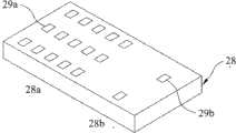
28:晶圆 28a:第一晶圆区28:
28b:第二晶圆区 29a:第一影像28b:
29b:第二影像 110:基板29b: Second Image 110: Substrate
112:导电层 114:介电层112: Conductive layer 114: Dielectric layer
120:抗反射涂覆层 122:光阻层120: anti-reflection coating 122: photoresist layer
200:基板 201、203、205:图案200: Substrate 201, 203, 205: Pattern
202、204、206:图案 207、209、211:图案202, 204, 206: pattern 207, 209, 211: pattern
208、210、212:图案 h1:聚焦面之间的差距208, 210, 212: pattern h1: gap between focal planes
Z:移动方向Z: direction of movement
具体实施方式Detailed ways
为更进一步阐述本发明为达成预定发明目的所采取的技术手段及功效,以下结合附图及较佳实施例,对依据本发明提出的在半导体制程中的微影系统及其方法其具体实施方式、结构、方法、步骤、特征及其功效,详细说明如后。In order to further explain the technical means and effects that the present invention takes to achieve the intended purpose of the invention, the specific implementation of the lithography system and its method in the semiconductor manufacturing process proposed according to the present invention will be described below in conjunction with the accompanying drawings and preferred embodiments , structure, method, step, feature and effect thereof, detailed description is as follows.
应了解以下说明书提供的许多不同的具体例或实施例,以完成本发明的不同特征。为了简化本说明书,元件及排列的特例说明如下。此等当然仅为实施例,且不欲受限于此。此外,本说明书在许多实施例中可能重复元件符号及/或字母。此种重复是为了简洁及清楚的目的,且并非本身表示所讨论的不同具体例及/或结构间的关联性。It should be appreciated that the following description provides many different embodiments, or embodiments, for implementing the various features of the invention. In order to simplify this description, specific examples of elements and arrangements are described below. These are of course only examples and are not intended to be limited thereto. In addition, the description may repeat element symbols and/or letters in many embodiments. Such repetition is for the purpose of brevity and clarity and does not in itself indicate a relatedness between the different embodiments and/or structures discussed.
为了平衡针对致密和疏松接触孔的个别DOFs,先前可行的技艺是使用具有双重曝光的双光罩。一般而言,第一光罩用于致密接触孔,而第二光罩则用于疏松接触孔。In order to balance the individual DOFs for dense and loose contact holes, it was previously possible to use a dual mask with double exposure. Generally speaking, the first mask is used for dense contact holes, and the second mask is used for loose contact holes.
然而,在微影制程期间交换光罩是耗费成本的。再者,使用双光罩亦可能造成覆盖不准确。However, exchanging reticles during the lithography process is costly. Furthermore, the use of dual masks may also result in inaccurate coverage.
因此,使用单一光罩于双重曝光以提供所需影像是合宜的。如以下的进一步说明,本说明书将揭示一种具有二个或更多聚焦面的单一光罩,以适应不同的曝光。Therefore, it is convenient to use a single mask for double exposure to provide the desired image. As further described below, this specification will disclose a single reticle with two or more focal planes to accommodate different exposures.
请参阅图1所示,是一种实施本发明的一个或更多实施例的微影方法的流程图,是绘示实施本发明的一个或更多实施例的简化的微影方法10。该方法由步骤12开始,首先是提供一种具有第一及第二聚焦面的光罩。随后为步骤14,配合使用第一聚焦面提供第一曝光于一晶圆,以在第一晶圆区中形成第一影像,以及随后的步骤16,配合使用第二聚焦面提供第二曝光于该晶圆,以在第二晶圆区中形成第二影像。Please refer to FIG. 1 , which is a flowchart of a lithography method for implementing one or more embodiments of the present invention, and illustrates a simplified lithography method 10 for implementing one or more embodiments of the present invention. The method starts from step 12. Firstly, a photomask having first and second focusing planes is provided. This is followed by step 14 of providing a first exposure to a wafer using the first focal plane to form a first image in the first wafer region, and subsequent step 16 of providing a second exposure using the second focal plane to The wafer is used to form a second image in the second wafer region.
方法10可用于制造许多半导体装置,例如记忆体装置(包含但不限于静态随机存储器(SRAM))、逻辑单元(包含但不限于金属氧化物半导体场效电晶体(MOSFET))及/或其他装置。方法10从步骤12开始,其中单一光罩中具有复数个聚焦面。Method 10 can be used to fabricate many semiconductor devices, such as memory devices (including but not limited to static random access memory (SRAM)), logic cells (including but not limited to metal oxide semiconductor field effect transistors (MOSFET)) and/or other devices . Method 10 begins at step 12 with a plurality of focal planes in a single reticle.
接着请参阅图2a所示,是一种实施本发明一个或更多实施例的微影系统的示意图。用于方法10的步骤12中的光罩24,是为部分经简化的例示微影系统。在本实施例中,光源21发出光束23,该光束23经聚光镜22聚光。因此,含有图案的光罩24均匀地受到经聚光镜22聚光后的光束27的照射。通过光罩24后的光束25是先受到投影镜头26聚焦后再投影于晶圆28。Next, please refer to FIG. 2 a , which is a schematic diagram of a lithography system implementing one or more embodiments of the present invention. The mask 24 used in step 12 of the method 10 is a simplified example of a partially lithographic system. In this embodiment, the light source 21 emits a light beam 23 , and the light beam 23 is condensed by a condenser lens 22 . Therefore, the mask 24 containing the pattern is evenly irradiated by the light beam 27 condensed by the condenser lens 22 . The light beam 25 passing through the mask 24 is first focused by the projection lens 26 and then projected onto the
接着请参阅图2b所示,是一种用于图2a的微影系统的光罩的部分示意图。光罩24可以为含有电子电路的显微影像的高精密度板。该光罩24可以包括许多材料,例如石英、钠钙(soda lime)、白冠玻璃及/或其他材料。一般而言,光罩24的一侧可含有一层铬,且可在铬层中蚀刻电子电路(通常称为几何形状)。光罩24的厚度可为技艺中已知的任一适合的厚度。Please refer to FIG. 2 b , which is a partial schematic diagram of a photomask used in the lithography system of FIG. 2 a . Reticle 24 may be a high precision plate containing a microscopic image of the electronic circuit. The reticle 24 may comprise many materials such as quartz, soda lime, white crown glass, and/or other materials. Generally, one side of the reticle 24 may contain a layer of chrome, and electronic circuitry (commonly referred to as geometry) may be etched into the chrome layer. The thickness of the mask 24 can be any suitable thickness known in the art.
在另一实施例中,光罩24包含第一聚焦面24a及第二聚焦面24b。第一聚焦面24a可包含致密图案23a(虽然亦可使用其他图案,但是图中仅绘示了致密接触孔)。在一实施例中,在第一聚焦面24a中的接触孔23a与另一接触孔分开约0.18微米至约0.36微米的距离。应理解其他距离亦可涵盖于本发明中。In another embodiment, the photomask 24 includes a first focusing plane 24a and a second focusing plane 24b. The first focusing surface 24a may include a dense pattern 23a (although other patterns may also be used, but only dense contact holes are shown in the figure). In one embodiment, a contact hole 23a in the first focusing plane 24a is separated from another contact hole by a distance of about 0.18 microns to about 0.36 microns. It should be understood that other distances are also contemplated by the present invention.
在另一实施例中,第二聚焦面24b可包含疏松图案23b(虽然亦可使用其他图案,但图中仅绘示了疏松接触孔)。在一实施例中,在第二聚焦面24b中的接触孔23b与另一接触孔分开约0.36微米的距离。应理解其他距离亦可涵盖于本发明中。In another embodiment, the second focusing surface 24b may include a loose pattern 23b (although other patterns may also be used, but only loose contact holes are shown in the figure). In one embodiment, the contact hole 23b in the second focusing plane 24b is separated from the other contact hole by a distance of about 0.36 microns. It should be understood that other distances are also contemplated by the present invention.
请再参阅图3a所示,图3a是图1的微影系统在中间处理阶段的选用元件的示意图。在一实施例中,第一聚焦面24a及第二聚焦面24b之间的差距h1可为约1微米至约10微米。然而,应理解差距h1可小于1微米或大于10微米。Please refer to FIG. 3 a again. FIG. 3 a is a schematic diagram of selected components of the lithography system of FIG. 1 in an intermediate processing stage. In one embodiment, the gap h1 between the first focusing plane 24a and the second focusing plane 24b may be about 1 micron to about 10 microns. However, it should be understood that the gap h1 may be less than 1 micron or greater than 10 microns.
请参阅图1、图3a及图3b所示,图3b是图3a及图3b的中间处理阶段中的部分半导体基板的示意图。在方法10的步骤14之后,配合使用第一聚焦面24a提供第一曝光,以在第一晶圆区28a中形成第一影像29a。在第一曝光期间,第一聚焦面24a可作为光罩聚焦面。在操作中,光束20a及光束20b是投影于晶圆28上,且来自第一聚焦面24a的图案可转移至对应的第一晶圆区28a。应理解虽然第二聚焦面24b失焦,但是光束20c及光束20b的投影聚焦点超过晶圆28。因此,第二聚焦面24b的影像不会转移至对应的第二晶圆区28b。Please refer to FIG. 1, FIG. 3a and FIG. 3b. FIG. 3b is a schematic diagram of a part of the semiconductor substrate in the intermediate processing stage of FIG. 3a and FIG. 3b. After step 14 of the method 10, a first exposure is provided in conjunction with the first focusing plane 24a to form a
在完成第一曝光步骤之后,光罩24可朝Z方向移动一段约差距h1的距离或任一其他适合的距离,使得第二聚焦面24b可供第二曝光聚焦。预期可藉任一机械或其他适合的构件移动光罩24。After the first exposure step is completed, the mask 24 can be moved toward the Z direction for a distance of about h1 or any other suitable distance, so that the second focusing surface 24b can be focused for the second exposure. It is contemplated that reticle 24 may be moved by any mechanical or other suitable means.
此时请参阅图1、图4a及图4b所示,图4a是图1的微影系统在中间处理阶段的选用元件的示意图,图4b是图3b的中间处理阶段中的部分半导体基板的示意图。在方法10的步骤16之后,配合使用第二聚焦面24b提供第二曝光,以在第二晶圆区28b中形成第二影像29b。在本实施例中,第二聚焦面24b可作为光罩聚焦面。因此,光束22c及光束22d是投影于晶圆28上,且来自第二聚焦面24b的图案可转移至对应的第二晶圆区28b。应理解虽然第一聚焦面24a失焦,但是光束22a及光束22b的投影聚焦点是在到达晶圆28之前。因此,第一聚焦面24a的影像不会转移至对应的第一晶圆区28a。Please refer to Fig. 1, Fig. 4a and Fig. 4b at this time. Fig. 4a is a schematic diagram of selected components in the intermediate processing stage of the lithography system of Fig. 1, and Fig. 4b is a schematic diagram of part of the semiconductor substrate in the intermediate processing stage of Fig. 3b . After step 16 of the method 10, a second exposure is provided in conjunction with the second focusing plane 24b to form a
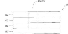
请参阅图5a及图5b所示,是图3b及图4b的部分半导体基板的断面示意图。在本实施例中,其是绘示在方法10之前(如图5a所示)及完成方法10之后(如图5b所示,晶圆28包含一基板110、一导电层112、一介电层114、一抗反射涂覆(ARC)层120及一光阻层122)的状态。Please refer to FIG. 5a and FIG. 5b , which are schematic cross-sectional views of part of the semiconductor substrate shown in FIG. 3b and FIG. 4b . In this embodiment, it is shown before the method 10 (as shown in FIG. 5a) and after the method 10 is completed (as shown in FIG. 5b, the
该基板110可以包含一种或多种绝缘体、导体及/或半导体层。举例来说,该基板110可以包含基础半导体,例如结晶硅、多晶硅、非结晶硅及/或锗;化合物半导体,例如碳化硅及/或砷化镓;合金半导体,例如硅化锗(SiGe)、磷化砷镓(GaAsP)、砷化铝镓(AlGaAs)及/或磷化铟镓(GaInP)。再者,该基板110可以包含块半导体(例如块硅),且此类块半导体可以包含磊晶硅层。其亦可或另外地包含绝缘半导体基板,例如绝缘体硅(SOI)基板或薄膜电晶体(TFT)基板。该基板110亦可或另外地包含多晶结构或多层化合物半导体结构。The
可以藉化学蒸气沉积(CVD)、电浆增强CVD(PECVD)、物理蒸气沉积(PVD)、离子PVD(I-PVD)、原子层沉积(ALD)、电镀及/或其他方法沉积导电层112.在形成导电层112期间可使用化学-机械平坦化及/或化学-机械研磨.导电层112的深度可在约1500埃与5000埃之间的范围内.举例来说,在一实施例中,深度可为约3500埃.该导电层112可以包含铝、铝合金、铜、铜合金、钨及/或其他导电材料.The
经由许多技术,包含(但是不限于)旋转涂布、PVD、PCD及/或其他方法,使ARC层120可沉积于导电层112上方。
在一实施例中,抗反射涂覆(ARC)层120(以下称为ARC层)可吸收不慎穿透光阻层122的光线。为了进行光吸收,ARC层120可含有具有高消光系数及/或相当厚度的材料。就另一方面而论,ARC层120的高系数可能造成ARC层120的高反射率,此不利于ARC层的功效。因此,预期ARC层120可具有约0.2至约0.5的系数值,且可具有厚度为约200毫微米。然而,应理解其他范围的硅数值及厚度亦可涵盖于本发明中。In one embodiment, the anti-reflective coating (ARC) layer 120 (hereinafter referred to as the ARC layer) can absorb light that accidentally penetrates the
另外,就ARC层120而言,亦可采用折射率匹配方式。在此情形中,ARC层120可含有一种具有折射率及厚度匹配于光线的材料。在操作中,一旦光线照在ARC层120,则部分光线从其中反射。此时,其他部分光线进入ARC层120中,且转换为具有转移相的光线,此与从ARC层120反射的第一部分光线产生干涉,因而造成光反射率减少。In addition, for the
ARC层120可考虑使用光吸收且折射率亦匹配者,以期接近所欲达成的结果。在某些情况下,因为ARC层120的移除可能不容易完成,则ARC层120可单纯地余留于介电层114的上方,并作为晶圆28的扩散障壁。The
在另一实施例中,光阻层122可以沉积于ARC层120的上方。可藉旋转涂覆及/或其他方法形成光阻层122。在操作中,将光阻溶液分配于ARC层120的表面上,并且快速地旋转晶圆28,直到光阻溶液几乎干燥为止。在一实施例中,光阻层122可为使用酸触媒的化学放大型阻剂。在此情形下,可藉溶解酸敏性聚合物于浇铸溶液中来调配光阻层。In another embodiment, a
在沉积光阻层后,在方法10(如上述)之后使晶圆28受到软烤及双重曝光。After depositing the photoresist layer,
此时请特别地参阅图5b所示,在已于导电层中图案化特征且已去除顶层(例如ARC层120及光阻层122)之后,介电层114可沉积于基板110的表面上及在导电层112周围。可藉化学气相沉积系统(CVD)、电浆辅助化学气相沉积系统(PECVD)、原子层沉积系统(ALD)、物理气相沉积系统(PVD)、高密度电浆系统(HDP)、旋转涂覆及/或其他方法形成介电层114。介电层114可为内金属介电层(IMD),且可含有高介电质(k)材料、低介电质(k)材料、二氧化硅聚酰亚胺、旋涂式玻璃(SOG)、掺氟硅酸盐玻璃(FSG)、Black
随后,利用其他步骤以形成完整的半导体装置。由于此等额外步骤是为技艺中已知,故在此不再赘述。Subsequently, other steps are utilized to form a complete semiconductor device. Since these additional steps are known in the art, they will not be repeated here.
应当理解上述实施例的许多变化可以涵盖于本案.在一实施例中,该光罩24可包含至少三个聚焦面以供至少三次独立的曝光,以取代前述的二个聚焦面24a及24b的实施例.在第二实施例中,该光罩24可包含至少三个聚焦面以供一或多次独立的曝光.在第三实施例中,在一次曝光中可同时使二个或多个聚焦面聚焦.在第四实施例中,第一聚焦面24a可以包含疏松图案,而第二聚焦面24b可以包含致密图案.在第五实施例中,取代在第一曝光后使光罩24朝Z方向移动,可调整光束以供第二曝光.在第六实施例中,方法10可应用于线图案(例如在第一曝光期间可形成致密的线组合,而在第二曝光期间可形成至少一疏松线).在第七实施例中且此刻请参阅图6所示,方法10可应用于基板200的致密图案.在一实施例中,可在第一曝光过程中形成某些选择图案,而可在第二曝光过程中形成其余的图案.在一实施例中,以奇数标出的图案(201、203、205、207、209以及211)可在第一曝光过程中形成,而以偶数标出的图案(202、204、206、208、210及212)可以在第二曝光过程中形成.此外,方法10可应用于非镶嵌、镶嵌或双重镶嵌程序.因此,本说明书涵盖许多变化润饰.It should be understood that many variations of the above-described embodiments can be included in this case. In one embodiment, the mask 24 can include at least three focal planes for at least three independent exposures, instead of the aforementioned two focal planes 24a and 24b Embodiment. In the second embodiment, the reticle 24 may comprise at least three focusing planes for one or more independent exposures. In the third embodiment, two or more The focal plane is focused. In the fourth embodiment, the first focal plane 24a may contain a loose pattern, while the second focal plane 24b may contain a dense pattern. In the fifth embodiment, instead of making the reticle 24 towards the Moving in the Z direction, the beam can be adjusted for the second exposure. In the sixth embodiment, the method 10 can be applied to line patterns (for example, a dense combination of lines can be formed during the first exposure, and at least a loose line). In the seventh embodiment and now referring to FIG. 6, the method 10 can be applied to a dense pattern of the substrate 200. In one embodiment, certain selected patterns can be formed during the first exposure process, The remaining patterns can be formed in the second exposure process. In one embodiment, the patterns marked with odd numbers (201, 203, 205, 207, 209, and 211) can be formed in the first exposure process, and the patterns marked with even numbers The marked patterns (202, 204, 206, 208, 210, and 212) can be formed in a second exposure process. In addition, method 10 can be applied to non-damascene, damascene or dual damascene procedures. Therefore, this specification covers many variations of retouching .
以上所述,仅是本发明的较佳实施例而已,并非对本发明作任何形式上的限制,虽然本发明已以较佳实施例揭露如上,然而并非用以限定本发明,任何熟悉本专业的技术人员,在不脱离本发明技术方案范围内,当可利用上述揭示的方法及技术内容作出些许的更动或修饰为等同变化的等效实施例,但是凡是未脱离本发明技术方案的内容,依据本发明的技术实质对以上实施例所作的任何简单修改、等同变化与修饰,均仍属于本发明技术方案的范围内。The above description is only a preferred embodiment of the present invention, and does not limit the present invention in any form. Although the present invention has been disclosed as above with preferred embodiments, it is not intended to limit the present invention. Anyone familiar with this field Those skilled in the art, without departing from the scope of the technical solution of the present invention, can use the method and technical content disclosed above to make some changes or modifications to equivalent embodiments with equivalent changes, but any content that does not depart from the technical solution of the present invention, Any simple modifications, equivalent changes and modifications made to the above embodiments according to the technical essence of the present invention still fall within the scope of the technical solutions of the present invention.
Claims (13)
Applications Claiming Priority (2)
| Application Number | Priority Date | Filing Date | Title |
|---|---|---|---|
| US11/054,458 | 2005-02-09 | ||
| US11/054,458US7601466B2 (en) | 2005-02-09 | 2005-02-09 | System and method for photolithography in semiconductor manufacturing |
Publications (2)
| Publication Number | Publication Date |
|---|---|
| CN1818791A CN1818791A (en) | 2006-08-16 |
| CN1818791Btrue CN1818791B (en) | 2010-05-12 |
Family
ID=36780376
Family Applications (1)
| Application Number | Title | Priority Date | Filing Date |
|---|---|---|---|
| CN2006100032671AExpired - Fee RelatedCN1818791B (en) | 2005-02-09 | 2006-02-08 | Photolithography system and method in semiconductor manufacturing process and photomask used therein |
Country Status (4)
| Country | Link |
|---|---|
| US (1) | US7601466B2 (en) |
| CN (1) | CN1818791B (en) |
| NL (1) | NL1031104C2 (en) |
| TW (1) | TWI306271B (en) |
Families Citing this family (9)
| Publication number | Priority date | Publication date | Assignee | Title |
|---|---|---|---|---|
| WO2009018846A1 (en)* | 2007-08-09 | 2009-02-12 | Carl Zeiss Smt Ag | Method of structuring a photosensitive material |
| US20090201474A1 (en)* | 2008-02-13 | 2009-08-13 | Sajan Marokkey | Semiconductor Devices and Methods of Manufacture Thereof |
| US8745554B2 (en)* | 2009-12-28 | 2014-06-03 | Taiwan Semiconductor Manufacturing Company, Ltd. | Practical approach to layout migration |
| SG11201505056WA (en)* | 2012-12-28 | 2015-08-28 | Hoya Corp | Substrate for mask blank, substrate with multilayer reflective film, reflective mask blank, reflective mask, method of manufacturing for substrate for mask blank, method of manufacturing for substrate with multilayer reflective film, and method of manufacturing semiconductor device |
| CN104460244A (en)* | 2013-12-30 | 2015-03-25 | 苏州矩阵光电有限公司 | Process for assisting integrated optical production by utilizing double exposure technology |
| US10274830B2 (en) | 2016-01-27 | 2019-04-30 | Taiwan Semiconductor Manufacturing Co., Ltd. | Method and apparatus for dynamic lithographic exposure |
| DE102017100340B4 (en) | 2016-01-27 | 2021-04-29 | Taiwan Semiconductor Manufacturing Co., Ltd. | Method of developing a photosensitive material and photolithography tool - US Pat |
| JP6951446B2 (en)* | 2016-12-20 | 2021-10-20 | エーファウ・グループ・エー・タルナー・ゲーエムベーハー | Equipment and methods for exposing photosensitive layers |
| WO2025145439A1 (en)* | 2024-01-05 | 2025-07-10 | Applied Materials, Inc. | Adjusting effective depth of focus |
Citations (4)
| Publication number | Priority date | Publication date | Assignee | Title |
|---|---|---|---|---|
| DE4232844A1 (en)* | 1992-09-30 | 1994-03-31 | Siemens Ag | Exposure method for optical projection lithography used in integrated circuit mfr. - applying imaged structure to non-planar surface of exposure mask to increase image sharpness |
| US5547788A (en)* | 1993-03-04 | 1996-08-20 | Samsung Electronic Co., Ltd. | Mask and method for manufacturing the same |
| US6368754B1 (en)* | 1998-11-13 | 2002-04-09 | Nec Corporation | Reticle used for fabrication of semiconductor device |
| US6498105B1 (en)* | 1999-06-01 | 2002-12-24 | Samsung Electronics Co., Ltd. | Method of forming fine patterns of a semiconductor device |
Family Cites Families (6)
| Publication number | Priority date | Publication date | Assignee | Title |
|---|---|---|---|---|
| US5308741A (en) | 1992-07-31 | 1994-05-03 | Motorola, Inc. | Lithographic method using double exposure techniques, mask position shifting and light phase shifting |
| US6190840B1 (en)* | 1997-06-18 | 2001-02-20 | Kabushiki Kaisha Toshiba | Resist pattern forming method |
| US6022644A (en)* | 1998-03-18 | 2000-02-08 | Taiwan Semiconductor Manufacturing Co., Ltd. | Mask containing subresolution line to minimize proximity effect of contact hole |
| US6803178B1 (en)* | 2001-06-25 | 2004-10-12 | Advanced Micro Devices, Inc. | Two mask photoresist exposure pattern for dense and isolated regions |
| US20030022112A1 (en)* | 2001-07-27 | 2003-01-30 | Juliana Arifin | Structuring method |
| US7052808B2 (en)* | 2003-02-11 | 2006-05-30 | Infineon Technologies Ag | Transmission mask with differential attenuation to improve ISO-dense proximity |
- 2005
- 2005-02-09USUS11/054,458patent/US7601466B2/ennot_activeExpired - Fee Related
- 2006
- 2006-02-07TWTW095104085Apatent/TWI306271B/ennot_activeIP Right Cessation
- 2006-02-08CNCN2006100032671Apatent/CN1818791B/ennot_activeExpired - Fee Related
- 2006-02-08NLNL1031104Apatent/NL1031104C2/enactiveSearch and Examination
Patent Citations (4)
| Publication number | Priority date | Publication date | Assignee | Title |
|---|---|---|---|---|
| DE4232844A1 (en)* | 1992-09-30 | 1994-03-31 | Siemens Ag | Exposure method for optical projection lithography used in integrated circuit mfr. - applying imaged structure to non-planar surface of exposure mask to increase image sharpness |
| US5547788A (en)* | 1993-03-04 | 1996-08-20 | Samsung Electronic Co., Ltd. | Mask and method for manufacturing the same |
| US6368754B1 (en)* | 1998-11-13 | 2002-04-09 | Nec Corporation | Reticle used for fabrication of semiconductor device |
| US6498105B1 (en)* | 1999-06-01 | 2002-12-24 | Samsung Electronics Co., Ltd. | Method of forming fine patterns of a semiconductor device |
Non-Patent Citations (1)
| Title |
|---|
| JP特开2000-206672A 2000.07.28 |
Also Published As
| Publication number | Publication date |
|---|---|
| US7601466B2 (en) | 2009-10-13 |
| NL1031104C2 (en) | 2007-12-14 |
| CN1818791A (en) | 2006-08-16 |
| TWI306271B (en) | 2009-02-11 |
| TW200629372A (en) | 2006-08-16 |
| US20060177778A1 (en) | 2006-08-10 |
| NL1031104A1 (en) | 2006-08-11 |
Similar Documents
| Publication | Publication Date | Title |
|---|---|---|
| CN1818791B (en) | Photolithography system and method in semiconductor manufacturing process and photomask used therein | |
| CN110389500B (en) | Method for manufacturing semiconductor device | |
| US10859902B2 (en) | Lithography mask and method | |
| US11086215B2 (en) | Extreme ultraviolet mask with reduced mask shadowing effect and method of manufacturing the same | |
| US8178289B2 (en) | System and method for photolithography in semiconductor manufacturing | |
| US10685846B2 (en) | Semiconductor integrated circuit fabrication with pattern-reversing process | |
| US9685367B2 (en) | Photomask for forming multiple layer patterns with a single exposure | |
| US20080292991A1 (en) | High fidelity multiple resist patterning | |
| JP2009290002A (en) | Method for manufacturing semiconductor integrated circuit apparatus | |
| CN107290929B (en) | Photomask with multiple shielding layers | |
| TW201824346A (en) | Semiconductor device manufacturing method | |
| US20050031967A1 (en) | Photomask, method for fabricating a pattern and method for manufacturing a semiconductor device | |
| US20230386838A1 (en) | Euv photomask and related methods | |
| US9280046B2 (en) | Method of fabricating mask | |
| KR100846678B1 (en) | A system and method for photolithography in semiconductor manufacturing | |
| JPH10312994A (en) | Manufacture of semiconductor device | |
| US20240053669A1 (en) | Euv photo masks and manufacturing method thereof | |
| US7968258B2 (en) | System and method for photolithography in semiconductor manufacturing | |
| US20050026049A1 (en) | Method for forming an opening on an alternating phase shift mask | |
| JPH06138647A (en) | Correcting method for photomask having phase shift layer |
Legal Events
| Date | Code | Title | Description |
|---|---|---|---|
| C06 | Publication | ||
| PB01 | Publication | ||
| C10 | Entry into substantive examination | ||
| SE01 | Entry into force of request for substantive examination | ||
| C14 | Grant of patent or utility model | ||
| GR01 | Patent grant | ||
| CF01 | Termination of patent right due to non-payment of annual fee | ||
| CF01 | Termination of patent right due to non-payment of annual fee | Granted publication date:20100512 |