CN1815733A - Semiconductor device and manufacturing method therefor - Google Patents
Semiconductor device and manufacturing method thereforDownload PDFInfo
- Publication number
- CN1815733A CN1815733ACNA2006100051403ACN200610005140ACN1815733ACN 1815733 ACN1815733 ACN 1815733ACN A2006100051403 ACNA2006100051403 ACN A2006100051403ACN 200610005140 ACN200610005140 ACN 200610005140ACN 1815733 ACN1815733 ACN 1815733A
- Authority
- CN
- China
- Prior art keywords
- circuit board
- semiconductor device
- connection
- semiconductor
- mentioned
- Prior art date
- Legal status (The legal status is an assumption and is not a legal conclusion. Google has not performed a legal analysis and makes no representation as to the accuracy of the status listed.)
- Granted
Links
Images


Classifications
- H—ELECTRICITY
- H01—ELECTRIC ELEMENTS
- H01L—SEMICONDUCTOR DEVICES NOT COVERED BY CLASS H10
- H01L25/00—Assemblies consisting of a plurality of semiconductor or other solid state devices
- H01L25/03—Assemblies consisting of a plurality of semiconductor or other solid state devices all the devices being of a type provided for in a single subclass of subclasses H10B, H10D, H10F, H10H, H10K or H10N, e.g. assemblies of rectifier diodes
- H01L25/04—Assemblies consisting of a plurality of semiconductor or other solid state devices all the devices being of a type provided for in a single subclass of subclasses H10B, H10D, H10F, H10H, H10K or H10N, e.g. assemblies of rectifier diodes the devices not having separate containers
- H01L25/065—Assemblies consisting of a plurality of semiconductor or other solid state devices all the devices being of a type provided for in a single subclass of subclasses H10B, H10D, H10F, H10H, H10K or H10N, e.g. assemblies of rectifier diodes the devices not having separate containers the devices being of a type provided for in group H10D89/00
- H—ELECTRICITY
- H01—ELECTRIC ELEMENTS
- H01L—SEMICONDUCTOR DEVICES NOT COVERED BY CLASS H10
- H01L24/00—Arrangements for connecting or disconnecting semiconductor or solid-state bodies; Methods or apparatus related thereto
- H01L24/93—Batch processes
- H01L24/95—Batch processes at chip-level, i.e. with connecting carried out on a plurality of singulated devices, i.e. on diced chips
- H01L24/97—Batch processes at chip-level, i.e. with connecting carried out on a plurality of singulated devices, i.e. on diced chips the devices being connected to a common substrate, e.g. interposer, said common substrate being separable into individual assemblies after connecting
- H—ELECTRICITY
- H01—ELECTRIC ELEMENTS
- H01L—SEMICONDUCTOR DEVICES NOT COVERED BY CLASS H10
- H01L23/00—Details of semiconductor or other solid state devices
- H01L23/48—Arrangements for conducting electric current to or from the solid state body in operation, e.g. leads, terminal arrangements ; Selection of materials therefor
- H01L23/488—Arrangements for conducting electric current to or from the solid state body in operation, e.g. leads, terminal arrangements ; Selection of materials therefor consisting of soldered or bonded constructions
- H01L23/498—Leads, i.e. metallisations or lead-frames on insulating substrates, e.g. chip carriers
- H01L23/49833—Leads, i.e. metallisations or lead-frames on insulating substrates, e.g. chip carriers the chip support structure consisting of a plurality of insulating substrates
- H—ELECTRICITY
- H01—ELECTRIC ELEMENTS
- H01L—SEMICONDUCTOR DEVICES NOT COVERED BY CLASS H10
- H01L25/00—Assemblies consisting of a plurality of semiconductor or other solid state devices
- H01L25/03—Assemblies consisting of a plurality of semiconductor or other solid state devices all the devices being of a type provided for in a single subclass of subclasses H10B, H10D, H10F, H10H, H10K or H10N, e.g. assemblies of rectifier diodes
- H01L25/10—Assemblies consisting of a plurality of semiconductor or other solid state devices all the devices being of a type provided for in a single subclass of subclasses H10B, H10D, H10F, H10H, H10K or H10N, e.g. assemblies of rectifier diodes the devices having separate containers
- H01L25/105—Assemblies consisting of a plurality of semiconductor or other solid state devices all the devices being of a type provided for in a single subclass of subclasses H10B, H10D, H10F, H10H, H10K or H10N, e.g. assemblies of rectifier diodes the devices having separate containers the devices being integrated devices of class H10
- H—ELECTRICITY
- H01—ELECTRIC ELEMENTS
- H01L—SEMICONDUCTOR DEVICES NOT COVERED BY CLASS H10
- H01L2224/00—Indexing scheme for arrangements for connecting or disconnecting semiconductor or solid-state bodies and methods related thereto as covered by H01L24/00
- H01L2224/01—Means for bonding being attached to, or being formed on, the surface to be connected, e.g. chip-to-package, die-attach, "first-level" interconnects; Manufacturing methods related thereto
- H01L2224/10—Bump connectors; Manufacturing methods related thereto
- H01L2224/15—Structure, shape, material or disposition of the bump connectors after the connecting process
- H01L2224/16—Structure, shape, material or disposition of the bump connectors after the connecting process of an individual bump connector
- H01L2224/161—Disposition
- H01L2224/16151—Disposition the bump connector connecting between a semiconductor or solid-state body and an item not being a semiconductor or solid-state body, e.g. chip-to-substrate, chip-to-passive
- H01L2224/16221—Disposition the bump connector connecting between a semiconductor or solid-state body and an item not being a semiconductor or solid-state body, e.g. chip-to-substrate, chip-to-passive the body and the item being stacked
- H01L2224/16225—Disposition the bump connector connecting between a semiconductor or solid-state body and an item not being a semiconductor or solid-state body, e.g. chip-to-substrate, chip-to-passive the body and the item being stacked the item being non-metallic, e.g. insulating substrate with or without metallisation
- H—ELECTRICITY
- H01—ELECTRIC ELEMENTS
- H01L—SEMICONDUCTOR DEVICES NOT COVERED BY CLASS H10
- H01L2224/00—Indexing scheme for arrangements for connecting or disconnecting semiconductor or solid-state bodies and methods related thereto as covered by H01L24/00
- H01L2224/01—Means for bonding being attached to, or being formed on, the surface to be connected, e.g. chip-to-package, die-attach, "first-level" interconnects; Manufacturing methods related thereto
- H01L2224/26—Layer connectors, e.g. plate connectors, solder or adhesive layers; Manufacturing methods related thereto
- H01L2224/31—Structure, shape, material or disposition of the layer connectors after the connecting process
- H01L2224/32—Structure, shape, material or disposition of the layer connectors after the connecting process of an individual layer connector
- H01L2224/321—Disposition
- H01L2224/32135—Disposition the layer connector connecting between different semiconductor or solid-state bodies, i.e. chip-to-chip
- H01L2224/32145—Disposition the layer connector connecting between different semiconductor or solid-state bodies, i.e. chip-to-chip the bodies being stacked
- H—ELECTRICITY
- H01—ELECTRIC ELEMENTS
- H01L—SEMICONDUCTOR DEVICES NOT COVERED BY CLASS H10
- H01L2224/00—Indexing scheme for arrangements for connecting or disconnecting semiconductor or solid-state bodies and methods related thereto as covered by H01L24/00
- H01L2224/01—Means for bonding being attached to, or being formed on, the surface to be connected, e.g. chip-to-package, die-attach, "first-level" interconnects; Manufacturing methods related thereto
- H01L2224/26—Layer connectors, e.g. plate connectors, solder or adhesive layers; Manufacturing methods related thereto
- H01L2224/31—Structure, shape, material or disposition of the layer connectors after the connecting process
- H01L2224/32—Structure, shape, material or disposition of the layer connectors after the connecting process of an individual layer connector
- H01L2224/321—Disposition
- H01L2224/32151—Disposition the layer connector connecting between a semiconductor or solid-state body and an item not being a semiconductor or solid-state body, e.g. chip-to-substrate, chip-to-passive
- H01L2224/32221—Disposition the layer connector connecting between a semiconductor or solid-state body and an item not being a semiconductor or solid-state body, e.g. chip-to-substrate, chip-to-passive the body and the item being stacked
- H01L2224/32225—Disposition the layer connector connecting between a semiconductor or solid-state body and an item not being a semiconductor or solid-state body, e.g. chip-to-substrate, chip-to-passive the body and the item being stacked the item being non-metallic, e.g. insulating substrate with or without metallisation
- H—ELECTRICITY
- H01—ELECTRIC ELEMENTS
- H01L—SEMICONDUCTOR DEVICES NOT COVERED BY CLASS H10
- H01L2224/00—Indexing scheme for arrangements for connecting or disconnecting semiconductor or solid-state bodies and methods related thereto as covered by H01L24/00
- H01L2224/01—Means for bonding being attached to, or being formed on, the surface to be connected, e.g. chip-to-package, die-attach, "first-level" interconnects; Manufacturing methods related thereto
- H01L2224/42—Wire connectors; Manufacturing methods related thereto
- H01L2224/47—Structure, shape, material or disposition of the wire connectors after the connecting process
- H01L2224/48—Structure, shape, material or disposition of the wire connectors after the connecting process of an individual wire connector
- H01L2224/481—Disposition
- H01L2224/48151—Connecting between a semiconductor or solid-state body and an item not being a semiconductor or solid-state body, e.g. chip-to-substrate, chip-to-passive
- H01L2224/48221—Connecting between a semiconductor or solid-state body and an item not being a semiconductor or solid-state body, e.g. chip-to-substrate, chip-to-passive the body and the item being stacked
- H01L2224/48225—Connecting between a semiconductor or solid-state body and an item not being a semiconductor or solid-state body, e.g. chip-to-substrate, chip-to-passive the body and the item being stacked the item being non-metallic, e.g. insulating substrate with or without metallisation
- H01L2224/48227—Connecting between a semiconductor or solid-state body and an item not being a semiconductor or solid-state body, e.g. chip-to-substrate, chip-to-passive the body and the item being stacked the item being non-metallic, e.g. insulating substrate with or without metallisation connecting the wire to a bond pad of the item
- H—ELECTRICITY
- H01—ELECTRIC ELEMENTS
- H01L—SEMICONDUCTOR DEVICES NOT COVERED BY CLASS H10
- H01L2224/00—Indexing scheme for arrangements for connecting or disconnecting semiconductor or solid-state bodies and methods related thereto as covered by H01L24/00
- H01L2224/73—Means for bonding being of different types provided for in two or more of groups H01L2224/10, H01L2224/18, H01L2224/26, H01L2224/34, H01L2224/42, H01L2224/50, H01L2224/63, H01L2224/71
- H01L2224/732—Location after the connecting process
- H01L2224/73201—Location after the connecting process on the same surface
- H01L2224/73215—Layer and wire connectors
- H—ELECTRICITY
- H01—ELECTRIC ELEMENTS
- H01L—SEMICONDUCTOR DEVICES NOT COVERED BY CLASS H10
- H01L2224/00—Indexing scheme for arrangements for connecting or disconnecting semiconductor or solid-state bodies and methods related thereto as covered by H01L24/00
- H01L2224/73—Means for bonding being of different types provided for in two or more of groups H01L2224/10, H01L2224/18, H01L2224/26, H01L2224/34, H01L2224/42, H01L2224/50, H01L2224/63, H01L2224/71
- H01L2224/732—Location after the connecting process
- H01L2224/73251—Location after the connecting process on different surfaces
- H01L2224/73253—Bump and layer connectors
- H—ELECTRICITY
- H01—ELECTRIC ELEMENTS
- H01L—SEMICONDUCTOR DEVICES NOT COVERED BY CLASS H10
- H01L2224/00—Indexing scheme for arrangements for connecting or disconnecting semiconductor or solid-state bodies and methods related thereto as covered by H01L24/00
- H01L2224/73—Means for bonding being of different types provided for in two or more of groups H01L2224/10, H01L2224/18, H01L2224/26, H01L2224/34, H01L2224/42, H01L2224/50, H01L2224/63, H01L2224/71
- H01L2224/732—Location after the connecting process
- H01L2224/73251—Location after the connecting process on different surfaces
- H01L2224/73265—Layer and wire connectors
- H—ELECTRICITY
- H01—ELECTRIC ELEMENTS
- H01L—SEMICONDUCTOR DEVICES NOT COVERED BY CLASS H10
- H01L2224/00—Indexing scheme for arrangements for connecting or disconnecting semiconductor or solid-state bodies and methods related thereto as covered by H01L24/00
- H01L2224/93—Batch processes
- H01L2224/95—Batch processes at chip-level, i.e. with connecting carried out on a plurality of singulated devices, i.e. on diced chips
- H01L2224/97—Batch processes at chip-level, i.e. with connecting carried out on a plurality of singulated devices, i.e. on diced chips the devices being connected to a common substrate, e.g. interposer, said common substrate being separable into individual assemblies after connecting
- H—ELECTRICITY
- H01—ELECTRIC ELEMENTS
- H01L—SEMICONDUCTOR DEVICES NOT COVERED BY CLASS H10
- H01L2225/00—Details relating to assemblies covered by the group H01L25/00 but not provided for in its subgroups
- H01L2225/03—All the devices being of a type provided for in the same main group of the same subclass of class H10, e.g. assemblies of rectifier diodes
- H01L2225/10—All the devices being of a type provided for in the same main group of the same subclass of class H10, e.g. assemblies of rectifier diodes the devices having separate containers
- H01L2225/1005—All the devices being of a type provided for in the same main group of the same subclass of class H10, e.g. assemblies of rectifier diodes the devices having separate containers the devices being integrated devices of class H10
- H01L2225/1011—All the devices being of a type provided for in the same main group of the same subclass of class H10, e.g. assemblies of rectifier diodes the devices having separate containers the devices being integrated devices of class H10 the containers being in a stacked arrangement
- H01L2225/1017—All the devices being of a type provided for in the same main group of the same subclass of class H10, e.g. assemblies of rectifier diodes the devices having separate containers the devices being integrated devices of class H10 the containers being in a stacked arrangement the lowermost container comprising a device support
- H01L2225/1023—All the devices being of a type provided for in the same main group of the same subclass of class H10, e.g. assemblies of rectifier diodes the devices having separate containers the devices being integrated devices of class H10 the containers being in a stacked arrangement the lowermost container comprising a device support the support being an insulating substrate
- H—ELECTRICITY
- H01—ELECTRIC ELEMENTS
- H01L—SEMICONDUCTOR DEVICES NOT COVERED BY CLASS H10
- H01L2225/00—Details relating to assemblies covered by the group H01L25/00 but not provided for in its subgroups
- H01L2225/03—All the devices being of a type provided for in the same main group of the same subclass of class H10, e.g. assemblies of rectifier diodes
- H01L2225/10—All the devices being of a type provided for in the same main group of the same subclass of class H10, e.g. assemblies of rectifier diodes the devices having separate containers
- H01L2225/1005—All the devices being of a type provided for in the same main group of the same subclass of class H10, e.g. assemblies of rectifier diodes the devices having separate containers the devices being integrated devices of class H10
- H01L2225/1011—All the devices being of a type provided for in the same main group of the same subclass of class H10, e.g. assemblies of rectifier diodes the devices having separate containers the devices being integrated devices of class H10 the containers being in a stacked arrangement
- H01L2225/1041—Special adaptations for top connections of the lowermost container, e.g. redistribution layer, integral interposer
- H—ELECTRICITY
- H01—ELECTRIC ELEMENTS
- H01L—SEMICONDUCTOR DEVICES NOT COVERED BY CLASS H10
- H01L2225/00—Details relating to assemblies covered by the group H01L25/00 but not provided for in its subgroups
- H01L2225/03—All the devices being of a type provided for in the same main group of the same subclass of class H10, e.g. assemblies of rectifier diodes
- H01L2225/10—All the devices being of a type provided for in the same main group of the same subclass of class H10, e.g. assemblies of rectifier diodes the devices having separate containers
- H01L2225/1005—All the devices being of a type provided for in the same main group of the same subclass of class H10, e.g. assemblies of rectifier diodes the devices having separate containers the devices being integrated devices of class H10
- H01L2225/1011—All the devices being of a type provided for in the same main group of the same subclass of class H10, e.g. assemblies of rectifier diodes the devices having separate containers the devices being integrated devices of class H10 the containers being in a stacked arrangement
- H01L2225/1047—Details of electrical connections between containers
- H01L2225/1058—Bump or bump-like electrical connections, e.g. balls, pillars, posts
- H—ELECTRICITY
- H01—ELECTRIC ELEMENTS
- H01L—SEMICONDUCTOR DEVICES NOT COVERED BY CLASS H10
- H01L24/00—Arrangements for connecting or disconnecting semiconductor or solid-state bodies; Methods or apparatus related thereto
- H01L24/73—Means for bonding being of different types provided for in two or more of groups H01L24/10, H01L24/18, H01L24/26, H01L24/34, H01L24/42, H01L24/50, H01L24/63, H01L24/71
- H—ELECTRICITY
- H01—ELECTRIC ELEMENTS
- H01L—SEMICONDUCTOR DEVICES NOT COVERED BY CLASS H10
- H01L2924/00—Indexing scheme for arrangements or methods for connecting or disconnecting semiconductor or solid-state bodies as covered by H01L24/00
- H01L2924/01—Chemical elements
- H01L2924/01004—Beryllium [Be]
- H—ELECTRICITY
- H01—ELECTRIC ELEMENTS
- H01L—SEMICONDUCTOR DEVICES NOT COVERED BY CLASS H10
- H01L2924/00—Indexing scheme for arrangements or methods for connecting or disconnecting semiconductor or solid-state bodies as covered by H01L24/00
- H01L2924/01—Chemical elements
- H01L2924/01005—Boron [B]
- H—ELECTRICITY
- H01—ELECTRIC ELEMENTS
- H01L—SEMICONDUCTOR DEVICES NOT COVERED BY CLASS H10
- H01L2924/00—Indexing scheme for arrangements or methods for connecting or disconnecting semiconductor or solid-state bodies as covered by H01L24/00
- H01L2924/01—Chemical elements
- H01L2924/01006—Carbon [C]
- H—ELECTRICITY
- H01—ELECTRIC ELEMENTS
- H01L—SEMICONDUCTOR DEVICES NOT COVERED BY CLASS H10
- H01L2924/00—Indexing scheme for arrangements or methods for connecting or disconnecting semiconductor or solid-state bodies as covered by H01L24/00
- H01L2924/01—Chemical elements
- H01L2924/01033—Arsenic [As]
- H—ELECTRICITY
- H01—ELECTRIC ELEMENTS
- H01L—SEMICONDUCTOR DEVICES NOT COVERED BY CLASS H10
- H01L2924/00—Indexing scheme for arrangements or methods for connecting or disconnecting semiconductor or solid-state bodies as covered by H01L24/00
- H01L2924/01—Chemical elements
- H01L2924/01078—Platinum [Pt]
- H—ELECTRICITY
- H01—ELECTRIC ELEMENTS
- H01L—SEMICONDUCTOR DEVICES NOT COVERED BY CLASS H10
- H01L2924/00—Indexing scheme for arrangements or methods for connecting or disconnecting semiconductor or solid-state bodies as covered by H01L24/00
- H01L2924/01—Chemical elements
- H01L2924/01082—Lead [Pb]
- H—ELECTRICITY
- H01—ELECTRIC ELEMENTS
- H01L—SEMICONDUCTOR DEVICES NOT COVERED BY CLASS H10
- H01L2924/00—Indexing scheme for arrangements or methods for connecting or disconnecting semiconductor or solid-state bodies as covered by H01L24/00
- H01L2924/15—Details of package parts other than the semiconductor or other solid state devices to be connected
- H01L2924/151—Die mounting substrate
- H01L2924/153—Connection portion
- H01L2924/1531—Connection portion the connection portion being formed only on the surface of the substrate opposite to the die mounting surface
- H01L2924/15311—Connection portion the connection portion being formed only on the surface of the substrate opposite to the die mounting surface being a ball array, e.g. BGA
- H—ELECTRICITY
- H01—ELECTRIC ELEMENTS
- H01L—SEMICONDUCTOR DEVICES NOT COVERED BY CLASS H10
- H01L2924/00—Indexing scheme for arrangements or methods for connecting or disconnecting semiconductor or solid-state bodies as covered by H01L24/00
- H01L2924/15—Details of package parts other than the semiconductor or other solid state devices to be connected
- H01L2924/151—Die mounting substrate
- H01L2924/153—Connection portion
- H01L2924/1532—Connection portion the connection portion being formed on the die mounting surface of the substrate
- H01L2924/1533—Connection portion the connection portion being formed on the die mounting surface of the substrate the connection portion being formed both on the die mounting surface of the substrate and outside the die mounting surface of the substrate
- H01L2924/15331—Connection portion the connection portion being formed on the die mounting surface of the substrate the connection portion being formed both on the die mounting surface of the substrate and outside the die mounting surface of the substrate being a ball array, e.g. BGA
- H—ELECTRICITY
- H05—ELECTRIC TECHNIQUES NOT OTHERWISE PROVIDED FOR
- H05K—PRINTED CIRCUITS; CASINGS OR CONSTRUCTIONAL DETAILS OF ELECTRIC APPARATUS; MANUFACTURE OF ASSEMBLAGES OF ELECTRICAL COMPONENTS
- H05K1/00—Printed circuits
- H05K1/02—Details
- H05K1/14—Structural association of two or more printed circuits
- H05K1/144—Stacked arrangements of planar printed circuit boards
Landscapes
- Engineering & Computer Science (AREA)
- Microelectronics & Electronic Packaging (AREA)
- Power Engineering (AREA)
- Computer Hardware Design (AREA)
- Physics & Mathematics (AREA)
- Condensed Matter Physics & Semiconductors (AREA)
- General Physics & Mathematics (AREA)
- Structures Or Materials For Encapsulating Or Coating Semiconductor Devices Or Solid State Devices (AREA)
- Lead Frames For Integrated Circuits (AREA)
- Cooling Or The Like Of Semiconductors Or Solid State Devices (AREA)
Abstract
Translated fromChinese
Description
Translated fromChinese技术领域Technical field
本发明涉及搭载有半导体元件的半导体装置、层叠多个半导体装置而成的半导体装置的层叠体以及该半导体装置的制造方法。The present invention relates to a semiconductor device on which a semiconductor element is mounted, a semiconductor device laminate in which a plurality of semiconductor devices are stacked, and a method for manufacturing the semiconductor device.
背景技术 Background technique
随着电子设备小型化、轻型化以及高性能化的发展,半导体装置的高密度安装化需求也在提高。基于这些需求,有人发明了将多个半导体元件搭载在一个半导体装置中的半导体装置。这样,就增加了安装基板每单位面积的半导体元件的安装密度。With the progress of miniaturization, weight reduction and high performance of electronic equipment, the demand for high-density mounting of semiconductor devices is also increasing. Based on these demands, a semiconductor device in which a plurality of semiconductor elements are mounted in one semiconductor device has been invented. Thus, the mounting density of the semiconductor elements per unit area of the mounting substrate is increased.
然而,对于将多个半导体元件搭载在一个半导体装置上的方式,有着制造技术上或产品可靠性上的限制。However, there are limitations in manufacturing technology and product reliability in the method of mounting a plurality of semiconductor elements on one semiconductor device.
为了将多个或多种半导体元件搭载在一个半导体装置中,会引起电路基板中布线密度增加的问题。具体来说,需要电路基板的多层布线化、引线键合或倒装片键合等的半导体元件与电路基板的连接部的高密度化等,电连接变得复杂。Mounting a plurality of or more types of semiconductor elements in one semiconductor device raises the problem of increased wiring density on a circuit board. Specifically, multilayer wiring of the circuit board, high density of the connection portion between the semiconductor element and the circuit board such as wire bonding or flip chip bonding are required, and the electrical connection becomes complicated.
此外,当将多种半导体元件搭载在一个半导体装置中时,还会产生该半导体装置的专用性高、半导体装置的通用性低的问题。Furthermore, when multiple types of semiconductor elements are mounted on one semiconductor device, there arises a problem that the specificity of the semiconductor device is high and the versatility of the semiconductor device is low.
为了解决这些问题,在日本国公开专利公报特开平4-280695号公报(1992年10月6日公开:以下称为专利文献1)中,公开了一种技术,其中不是将需要的全部半导体元件搭载于一个半导体装置中,而是将某几个半导体元件搭载在一个半导体装置中,进而层叠相同或其他的半导体装置,将该层叠体作成一个半导体装置。这样一来,在保证了被要求的安装密度的同时,解决了制造上以及可靠性上的问题,而且能确保半导体装置的通用性。In order to solve these problems, in Japanese Laid-Open Patent Publication No. Hei 4-280695 (published on October 6, 1992: hereinafter referred to as Patent Document 1), a technique is disclosed in which not all semiconductor elements that will be required Instead of being mounted in one semiconductor device, certain semiconductor elements are mounted in one semiconductor device, and then the same or other semiconductor devices are stacked to form a semiconductor device from the stacked body. In this way, while ensuring the required mounting density, problems in manufacturing and reliability are solved, and the versatility of the semiconductor device can be ensured.
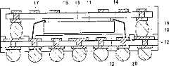
图10表示专利文献1的半导体装置的剖面图。在专利文献1的现有技术中,通过在搭载有半导体元件101的电路基板102上设置通孔103,使电路基板102的表背面能够导通。此外,在电路基板102的上表面一侧(半导体元件101的搭载侧),半导体元件101通过引线键合法连接到电路基板102中的连接用焊盘的一部分上,半导体元件101和键合线通过密封树脂105密封。此外,密封树脂105并不将电路基板102的整个上表面密封,而是将外部端子连接部104露出。FIG. 10 shows a cross-sectional view of the semiconductor device of Patent Document 1. As shown in FIG. In the prior art of Patent Document 1, the front and back surfaces of the circuit board 102 are electrically connected by providing the through holes 103 in the circuit board 102 on which the semiconductor element 101 is mounted. In addition, on the upper surface side of the circuit board 102 (the mounting side of the semiconductor element 101), the semiconductor element 101 is connected to a part of the connection pads in the circuit board 102 by wire bonding, and the semiconductor element 101 and the bonding wire pass through Sealing resin 105 seals. In addition, the sealing resin 105 does not seal the entire upper surface of the circuit board 102 but exposes the external
图11表示层叠图10所示的半导体装置而成的层叠体的剖面图。在该层叠体中,层叠图10所示的半导体装置彼此,通过导电体106将电路基板102之间连接起来。即,导电体106将在下侧的半导体装置的上表面露出的外部端子连接部104与在上侧的半导体装置的下表面露出的背面电极焊盘连接起来,由此,使层叠的多个半导体装置电连接。上述背面电极焊盘利用外部端子连接部104与通孔103而导通。FIG. 11 is a cross-sectional view of a stacked body in which the semiconductor devices shown in FIG. 10 are stacked. In this laminated body, semiconductor devices shown in FIG. That is, the
在专利文献1所述的发明中,除了连接半导体元件101与外部端子连接部104的布线以外,还需要用于使上下层叠的半导体装置彼此电连接的布线。由此,会产生以下问题:电路基板102中的布线变复杂,电路基板102变大,半导体装置的平面尺寸比半导体元件101大很多。In the invention described in Patent Document 1, in addition to the wiring for connecting the semiconductor element 101 and the external
为了避免这一问题,可举出日本国公开专利公报特开2004-172157号公报(2004年6月17日公开:以下称为专利文献2)中所示的现有技术。图12表示专利文献2的半导体装置的剖面图。In order to avoid this problem, the prior art disclosed in Japanese Laid-Open Patent Publication No. 2004-172157 (published on June 17, 2004: hereinafter referred to as Patent Document 2) can be cited. FIG. 12 shows a cross-sectional view of the semiconductor device of Patent Document 2. As shown in FIG.
在专利文献2的现有技术中,将半导体元件111搭载于电路基板112上,将它们用引线113连接起来,再通过粘合材料115将连接用电路基板114搭载在半导体元件111上。该连接用电路基板114在将其他的半导体装置层叠于图12所示的半导体装置的上一级(upperstage)的情况下,用于与层叠在上一级的半导体装置的电连接,在该连接用电路基板114上设有外部端子连接部116。连接用电路基板114通过引线117与电路基板112连接。In the prior art of Patent Document 2, a semiconductor element 111 is mounted on a circuit board 112 , they are connected by wires 113 , and a connecting circuit board 114 is mounted on the semiconductor element 111 through an adhesive material 115 . This connection circuit board 114 is used for electrical connection with the semiconductor device stacked on the upper stage when another semiconductor device is stacked on the upper stage (upper stage) of the semiconductor device shown in FIG. The external terminal connection portion 116 is provided on the circuit board 114 for use. The connection circuit board 114 is connected to the circuit board 112 through a lead wire 117 .
另外,引线113和117通过密封树脂118进行密封。进而,在电路基板112的下表面设有外部连接端子119。In addition, the leads 113 and 117 are sealed by a sealing resin 118 . Furthermore, external connection terminals 119 are provided on the lower surface of the circuit board 112 .
在图12所示的半导体装置中,能够将用于电连接层叠在上一级的半导体装置的布线设置在连接用电路基板114上,而不是电路基板112上。由此,就有这样的优点:能够防止电路基板112和连接用电路基板114两者中布线的复杂化,从而抑制两基板平面尺寸的增加,能够使半导体装置小型化。In the semiconductor device shown in FIG. 12 , wiring for electrically connecting a semiconductor device stacked on an upper stage can be provided on the connection circuit board 114 instead of the circuit board 112 . Thereby, there is an advantage that the complexity of wiring in both the circuit board 112 and the connection circuit board 114 can be prevented, and the increase in the planar size of both boards can be suppressed, thereby enabling miniaturization of the semiconductor device.
然而,在专利文献2的现有技术中,连接用电路基板114与电路基板112的连接方法是利用引线117的引线键合法。由此,在连接用电路基板114上需要引线117的回路高度和对其密封的密封树脂118的高度,会造成半导体装置的总高即半导体装置的厚度变大的问题。However, in the prior art of Patent Document 2, the method of connecting the circuit board 114 for connection and the circuit board 112 is the wire bonding method using the wire 117 . Therefore, the loop height of the lead wire 117 and the height of the sealing resin 118 sealing it are required on the connection circuit board 114 , which causes a problem that the overall height of the semiconductor device, that is, the thickness of the semiconductor device increases.
另外,在图12所示的半导体装置中,由于半导体元件111与电路基板112的连接是引线键合,所以连接用电路基板114被限定为其平面尺寸小于位于其下方的半导体元件111。In addition, in the semiconductor device shown in FIG. 12 , since the connection between the semiconductor element 111 and the circuit board 112 is wire bonding, the connecting circuit board 114 is limited in planar size to be smaller than the semiconductor element 111 located therebelow.
由这一点,加之连接用电路基板114与电路基板112的连接方法是利用引线117,所以在连接用电路基板114中能够配置外部端子连接部116的平面区域变小。由此,会对能配置在连接用电路基板114上的外部端子连接部116的数目或配置间隔造成限制,产生不能增加安装密度的问题。From this point, and the connecting method of the connecting circuit board 114 and the circuit board 112 using the lead wire 117, the planar area where the external terminal connecting portion 116 can be arranged in the connecting circuit board 114 is reduced. As a result, the number of external terminal connection portions 116 that can be arranged on the connection circuit board 114 and the arrangement interval are limited, and there arises a problem that the mounting density cannot be increased.
另外,在专利文献2所示的半导体装置中,虽然也能够在电路基板112上层叠并搭载多个半导体元件,但是这时就限定为上一级(upper)的半导体元件其平面尺寸要小于下一级(lower)的半导体元件。这样一来,当在电路基板112上层叠多个半导体元件时,其层叠数越增加,连接用电路基板114的面积就变得越小,使上述安装密度的问题凸显。In addition, in the semiconductor device disclosed in Patent Document 2, although a plurality of semiconductor elements can be stacked and mounted on the circuit board 112, it is limited in this case that the upper semiconductor element has a smaller planar size than the lower semiconductor element. A lower semiconductor component. In this way, when a plurality of semiconductor elements are stacked on the circuit board 112, the area of the connection circuit board 114 becomes smaller as the number of stacks increases, and the problem of the above-mentioned mounting density becomes prominent.
另外,当将其他的半导体装置搭载在连接用电路基板114上形成层叠体时,由配置在上一级的半导体装置工作产生的热量大部分都经由连接用电路基板114和粘合材料115传到半导体元件111,进而从半导体元件111经由电路基板112和外部连接端子119传向安装基板进行散热。In addition, when other semiconductor devices are mounted on the circuit board 114 for connection to form a laminated body, most of the heat generated by the operation of the semiconductor device arranged on the upper stage is transferred to the semiconductor device through the circuit board 114 for connection and the adhesive material 115. The semiconductor element 111 further transmits heat from the semiconductor element 111 to the mounting substrate via the circuit board 112 and the external connection terminal 119 .
由于粘合材料115的厚度较薄,所以连接用电路基板114的热量很容易传向半导体元件111,又由于半导体元件111与电路基板112之间也经由粘合材料等,所以连接用电路基板114的热量就比较容易传到安装基板上。Since the thickness of the adhesive material 115 is relatively thin, the heat of the circuit board 114 for connection is easily transmitted to the semiconductor element 111, and since the semiconductor element 111 and the circuit board 112 are also passed through the adhesive material, etc., the circuit board 114 for connection The heat is more easily transferred to the mounting substrate.
然而,当因半导体元件111的工作也有发热时,层叠在连接用电路基板114上的半导体装置工作所产生的热量就较难传导到连接用电路基板114上。这是由热的性质决定的,即热的移动难易度与温差的大小成正比。However, when heat is generated by the operation of the semiconductor element 111, the heat generated by the operation of the semiconductor device laminated on the connection circuit board 114 is less likely to be conducted to the connection circuit board 114. This is determined by the nature of heat, that is, the ease of movement of heat is proportional to the size of the temperature difference.
另外,由于作为将连接用电路基板114和电路基板112连接起来的另一条路径的导电体是引线117,所以能够传导的热量很少,对于散热的贡献很小。In addition, since the lead wire 117 is the conductor as another path connecting the connecting circuit board 114 and the circuit board 112 , the amount of heat that can be conducted is small, and the contribution to heat dissipation is small.
综上所述,当在专利文献2的半导体装置上层叠了其他的半导体装置并且在某个半导体装置中因半导体元件的工作而发热时,就会产生层叠在上一级的半导体装置的散热性低下的问题。In summary, when other semiconductor devices are stacked on the semiconductor device of Patent Document 2 and heat is generated by the operation of semiconductor elements in a certain semiconductor device, the heat dissipation of the semiconductor device stacked on the upper stage will occur. Lower problem.
发明内容Contents of the invention
本发明的目的在于:实现一种小而薄的半导体装置,其中,对于用于与层叠在上一级的半导体装置或电子部件的连接的外部连接用端子,其在配置上的制约较少,能够提高安装密度,并且散热性能优良。It is an object of the present invention to realize a small and thin semiconductor device in which there are few restrictions on the arrangement of external connection terminals used for connection to semiconductor devices or electronic components stacked on the upper stage. The mounting density can be increased, and the heat dissipation performance is excellent.
本发明的半导体装置为了达到上述目的,在电路基板上搭载至少一个半导体元件而成的半导体装置中,在位于最上层的半导体元件的上表面搭载具备外部端子连接部的连接用电路基板,上述连接用电路基板的下表面与上述电路基板的上表面用导电体端子连接,上述电路基板与上述连接用电路基板之间通过密封树脂进行密封。In the semiconductor device of the present invention, in order to achieve the above objects, in a semiconductor device in which at least one semiconductor element is mounted on a circuit substrate, a circuit substrate for connection having an external terminal connection portion is mounted on the upper surface of the semiconductor element positioned on the uppermost layer. The lower surface of the circuit board is connected to the upper surface of the circuit board by conductor terminals, and the circuit board and the connection circuit board are sealed with a sealing resin.
按照上述结构,具备外部端子连接部的连接用电路基板搭载于半导体元件上,连接用电路基板的下表面与电路基板的上表面通过导电体端子连接。由此,就能将用于电连接层叠在上一级的半导体装置的布线设在连接用电路基板上,而不是电路基板上。因此,就能够防止电路基板和连接用电路基板两者中布线的复杂化,从而能够抑制两基板平面尺寸的增加。According to the above configuration, the connection circuit board provided with the external terminal connection portion is mounted on the semiconductor element, and the lower surface of the connection circuit board is connected to the upper surface of the circuit board through the conductor terminal. Accordingly, the wiring for electrically connecting the semiconductor device stacked on the upper stage can be provided on the connection circuit board instead of the circuit board. Therefore, it is possible to prevent complication of wiring in both the circuit board and the circuit board for connection, and it is possible to suppress an increase in the planar size of both boards.
另外,连接用电路基板的下表面与电路基板的上表面不使用引线键合而是使用端子形状的导电体端子进行连接,由此,就不需要在用引线键合连接时所需的、连接用电路基板上的引线回路高度和密封引线键合的密封树脂部分的高度。因此,在上述半导体装置中,能够实现小型化和薄型化。In addition, the lower surface of the circuit board for connection and the upper surface of the circuit board are connected using a terminal-shaped conductor terminal instead of using wire bonding, so that there is no need for a connection required when connecting with wire bonding. Use the height of the lead loop on the circuit board and the height of the sealing resin portion that seals the wire bonding. Therefore, in the above-described semiconductor device, miniaturization and thinning can be achieved.
而且,在上述半导体装置中,由于连接用电路基板的下表面与电路基板的上表面通过导电体端子相连接,所以不存在连接用电路基板要比位于其下方的半导体元件平面尺寸小的限制。因此,连接用电路基板可以配备为具有与电路基板几乎相同面积的基板,能够扩大连接用电路基板中能配置外部端子连接部的平面区域。Furthermore, in the above-mentioned semiconductor device, since the lower surface of the connection circuit board is connected to the upper surface of the circuit board through conductor terminals, there is no restriction that the connection circuit board should be smaller in planar size than the semiconductor element located below it. Therefore, the circuit board for connection can be provided as a board having almost the same area as the circuit board, and the planar area in which the external terminal connection portion can be arranged in the circuit board for connection can be enlarged.
另外,本发明的半导体装置的层叠体为了达成上述目的,在上述记载的半导体装置上层叠配置其他的半导体装置或其他的电子部件,上述半导体装置的上述外部端子连接部与其上一级的其他半导体装置或其他电子部件通过导电体连接起来。In addition, in order to achieve the above object, the laminated body of the semiconductor device of the present invention is to stack and arrange other semiconductor devices or other electronic components on the above-mentioned semiconductor device, and the above-mentioned external terminal connection part of the above-mentioned semiconductor device and other semiconductor devices on the upper stage Devices or other electronic components connected by electrical conductors.
按照上述结构,通过在半导体装置上层叠配置其他的半导体装置或者其他的电子部件,从而在保证所要求的安装密度的同时,也解决了制造上和可靠性上的问题,并且能够确保半导体装置的通用性。According to the above structure, by stacking and disposing other semiconductor devices or other electronic components on the semiconductor device, while ensuring the required mounting density, problems in manufacturing and reliability are also solved, and the reliability of the semiconductor device can be ensured. Versatility.
此外,配置在上一级的半导体装置(或电子部件)的工作所产生的热量通过下一级的半导体装置中的经由连接用电路基板、导电体端子、电路基板、外部连接用端子的路径而传递到安装基板。由此,可以提高层叠在上一级的半导体装置或电子部件的散热特性。In addition, the heat generated by the operation of the semiconductor device (or electronic component) arranged on the upper stage is dissipated through the path through the circuit board for connection, the conductor terminal, the circuit board, and the terminal for external connection in the semiconductor device at the next stage. passed to the mounting substrate. Thereby, the heat radiation characteristic of the semiconductor device or electronic component laminated|stacked at the upper stage can be improved.
另外,为了达到上述目的,本发明的半导体装置的制造方法包括如下工序:将半导体元件搭载在电路基板上,并将该半导体元件与该电路基板电连接;将导电体端子搭载在上述电路基板上;将具备外部端子连接部的连接用电路基板搭载在上述半导体元件上,并且将上述连接用电路基板的下表面与搭载在上述电路基板上的导电体端子连接起来;将上述电路基板与上述连接用电路基板之间用树脂密封;以及将外部连接端子搭载在上述电路基板的下表面。In addition, in order to achieve the above object, the manufacturing method of the semiconductor device of the present invention includes the steps of: mounting a semiconductor element on a circuit board, and electrically connecting the semiconductor element to the circuit board; mounting conductor terminals on the circuit board. ; The connection circuit board provided with the external terminal connection part is mounted on the above-mentioned semiconductor element, and the lower surface of the above-mentioned connection circuit board is connected to the conductor terminal mounted on the above-mentioned circuit board; sealing with resin between the circuit boards; and mounting external connection terminals on the lower surface of the circuit board.
另外,为了达到上述目的,本发明的半导体装置的其他制造方法包括下述工序:将半导体元件搭载在框架状的电路基板上,并将该半导体元件与该电路基板电连接;将导电体端子搭载在上述电路基板上;将具备外部端子连接部的框架状的连接用电路基板搭载在上述半导体元件上,并且将上述连接用电路基板的下表面与搭载在上述电路基板上的导电体端子连接起来;将上述电路基板与上述连接用电路基板之间用树脂密封;将外部连接端子搭载在上述电路基板的下表面;以及从框架切出各个半导体装置。In addition, in order to achieve the above object, another manufacturing method of the semiconductor device of the present invention includes the following steps: mounting a semiconductor element on a frame-shaped circuit board, and electrically connecting the semiconductor element to the circuit board; On the above-mentioned circuit board; a frame-shaped connecting circuit board provided with an external terminal connection portion is mounted on the above-mentioned semiconductor element, and the lower surface of the above-mentioned connecting circuit board is connected to the conductor terminal mounted on the above-mentioned circuit board. ; sealing the space between the circuit board and the connection circuit board with resin; mounting external connection terminals on the lower surface of the circuit board; and cutting out individual semiconductor devices from the frame.
按照上述结构,就能够制造出具有如上所述特征的半导体装置。According to the above-mentioned structure, it is possible to manufacture a semiconductor device having the above-mentioned features.
另外,使用与多个部分的半导体装置相对应的框架状的电路基板和框架状的连接用电路基板,同时形成多个部分的半导体装置,最后通过切成半导体装置的各个片的工序来制造半导体装置,在这样的方法中,不需要树脂密封时的模具,能够适应任意尺寸的半导体装置的制造,并能够实现成本的降低。In addition, using a frame-shaped circuit board corresponding to a plurality of parts of the semiconductor device and a frame-shaped connection circuit board, a plurality of parts of the semiconductor device are formed at the same time, and finally the semiconductor device is manufactured by cutting into individual pieces of the semiconductor device. In such a method, a mold for resin sealing is not required, and it is possible to adapt to the manufacture of semiconductor devices of any size, and it is possible to achieve cost reduction.
本发明的进一步的其他目的、特征和优点通过以下所示的记载就会充分清楚了。另外,本发明的优势通过参照附图的下述说明就会明白了。Further other objects, features, and advantages of the present invention will be fully apparent from the description below. In addition, advantages of the present invention will become clear from the following description with reference to the accompanying drawings.
附图说明Description of drawings
图1表示本发明的实施方式,是表示实施方式1的半导体装置的结构的剖面图。FIG. 1 shows an embodiment of the present invention, and is a cross-sectional view showing the structure of a semiconductor device according to the first embodiment.
图2是表示实施方式1的半导体装置的变形例的剖面图。2 is a cross-sectional view showing a modified example of the semiconductor device of Embodiment 1. FIG.
图3是表示实施方式1的半导体装置的变形例的剖面图。3 is a cross-sectional view showing a modified example of the semiconductor device of Embodiment 1. FIG.
图4是表示实施方式1的半导体装置的变形例的剖面图。4 is a cross-sectional view showing a modified example of the semiconductor device of Embodiment 1. FIG.
图5是表示实施方式2的半导体装置的结构的剖面图。5 is a cross-sectional view showing the structure of a semiconductor device according to Embodiment 2. FIG.
图6是表示实施方式2的半导体装置的变形例的剖面图。6 is a cross-sectional view showing a modified example of the semiconductor device of Embodiment 2. FIG.
图7是表示实施方式3的半导体装置的结构的剖面图。7 is a cross-sectional view showing the structure of a semiconductor device according to Embodiment 3. FIG.
图8(a)~图8(d)是表示实施方式4的半导体装置的制造工序的剖面图。8( a ) to 8( d ) are cross-sectional views showing the manufacturing steps of the semiconductor device according to the fourth embodiment.
图9(a)~图9(e)是表示实施方式4的半导体装置的制造工序的变形例的剖面图。9( a ) to 9( e ) are cross-sectional views showing modified examples of the manufacturing process of the semiconductor device according to the fourth embodiment.
图10是表示现有的半导体装置的结构的剖面图。FIG. 10 is a cross-sectional view showing the structure of a conventional semiconductor device.
图11是表示层叠多个图10的半导体装置而成的层叠体的结构的剖面图。FIG. 11 is a cross-sectional view showing the structure of a laminate in which a plurality of semiconductor devices of FIG. 10 are stacked.
图12是表示现有的半导体装置的结构的剖面图。FIG. 12 is a cross-sectional view showing the structure of a conventional semiconductor device.
具体实施方式 Detailed ways
下面,基于附图对本发明的一实施方式进行说明。另外,以下所示的各实施方式是将本发明具体化的示例,而不是对本发明技术范围的限定。Hereinafter, an embodiment of the present invention will be described based on the drawings. In addition, each embodiment shown below is the example which actualized this invention, and does not limit the technical scope of this invention.
[实施方式1][Embodiment 1]
在图1中表示本发明的实施方式1的半导体装置的结构。FIG. 1 shows the structure of a semiconductor device according to Embodiment 1 of the present invention.
如图1所示,上述半导体装置中,半导体元件11经由粘合材料13连接在电路基板12上,半导体元件11与电路基板12通过引线14电连接。As shown in FIG. 1 , in the above-mentioned semiconductor device, a
另外,具有外部端子连接部17的连接用电路基板15经由粘合材料16连接在半导体元件11上,连接用电路基板15的下表面与电路基板12的上表面通过导电体端子18电连接。对于导电体端子18,能够采用焊接端子、金属凸块、导电胶、导电树脂等。导电胶、导电树脂能够通过掩模印刷法或者利用分配器从喷嘴喷出进行涂敷的方法等来形成在电路基板12上。Furthermore, a
对导电体端子18使用焊接端子或金属凸块时,由于具有高弹性,故有容易保持高度恒定的性质。另一方面,对导电体端子18采用导电胶或导电树脂时,由于这些材料在固化前较柔软,所以在搭载或者涂敷在电路基板12上之后,因将连接用电路基板15搭载在半导体元件11上时的压力而容易发生变形,具有容易得到目标高度/形状的性质。When a solder terminal or a metal bump is used as the
在上述半导体装置中,电路基板12与连接用电路基板15之间,即在电路基板12与连接用电路基板15之间配置的半导体元件11、引线14以及导电体端子18,通过密封树脂19进行密封。另外,密封树脂19以使外部端子连接部17与连接用电路基板15的一部分露出的方式来密封该半导体装置。在电路基板12的下表面上设有由导电体制成的外部连接端子20。外部连接端子20用于将上述半导体装置连接在安装电路板上。In the above-mentioned semiconductor device, between the
在上述结构的半导体装置中,具有外部端子连接部17的连接用电路基板15经由粘合材料16搭载在半导体元件11上,连接用电路基板15的下表面与电路基板12的上表面通过导电体端子18相连接。由此,就能将用于电连接层叠在上一级的半导体装置的布线设在连接用电路基板15上,而不是电路基板12上。因此,就能够防止电路基板12和连接用电路基板15两者中布线的复杂化,从而能够抑制两基板平面尺寸的增加。In the semiconductor device of the above-mentioned structure, the
另外,连接用电路基板15的下表面与电路基板12的上表面不使用引线键合而是使用端子形状的导电体端子18进行连接,由此,就不需要在用引线键合连接时所需的、连接用电路基板15上的引线回路高度和密封引线键合的密封树脂部分的高度。因此,在上述半导体装置中,能够实现小型化和薄型化。In addition, the lower surface of the
而且,在上述半导体装置中,由于连接用电路基板15的下表面与电路基板12的上表面通过导电体端子18相连接,所以不存在连接用电路基板15要比位于其下方的半导体元件11平面尺寸小的限制。因此,连接用电路基板15可以配备为具有与电路基板12几乎相同面积的基板,能够扩大连接用电路基板15中能配置外部端子连接部17的平面区域。Moreover, in the above-mentioned semiconductor device, since the lower surface of the
另外,利用图2至图4说明本实施方式1的半导体装置的变形例。In addition, a modified example of the semiconductor device according to Embodiment 1 will be described with reference to FIGS. 2 to 4 .
在图1所示的半导体装置中,密封树脂19形成为覆盖连接用电路基板15的上表面的一部分,但是本发明并不限于此,如图2所示,密封树脂19也可以是仅覆盖连接用电路基板15的下表面和侧面并使连接用电路基板15的整个上表面从密封树脂19露出的结构。或者,如图3所示,也可以使连接用电路基板15的整个上表面和侧面的至少一部分露出。通过成为使连接用电路基板15的整个上表面露出,从而能将外部端子连接部17配置在连接用电路基板15上的整个面上。In the semiconductor device shown in FIG. 1, the sealing
另外,在图1所示的半导体装置中,半导体元件11与电路基板12的连接是引线键合,但是本发明并不限于此,也可以是如图2所示的倒装片连接或者用导电树脂的连接。当对半导体元件11和电路基板12的连接采用倒装片连接时,具有能够降低封装高度的优点。In addition, in the semiconductor device shown in FIG. 1, the connection between the
另外,在图1所示的半导体装置中,粘合材料16仅形成在半导体元件11上,但是本发明并不限于此,如图3所示,也可以将粘合材料16形成在连接用电路基板15的整个下表面。这时,引线14也可以被粘合材料16覆盖住一部分。In addition, in the semiconductor device shown in FIG. 1, the
另外,如图4所示的半导体装置成为在图1所示的半导体装置中使用导电体端子21取代导电体端子1的结构。导电体端子21是其中持有核21A并在核21A的外侧具有导电层21B的端子。核21A可以是导电体也可以是绝缘体,由金属或者树脂构成。In addition, the semiconductor device shown in FIG. 4 has a structure in which the
在上述半导体装置中,通过导电体端子21持有核21A,从而导电体端子21的高度容易保持为恒定,能够保证连接用电路基板15与电路基板12的连接稳定性。特别地,只要核21A比存在于其外侧的导电层21B硬,那么当在制造本半导体装置的工序中进行高温下的处理时,容易将导电体端子21的高度保持为恒定的效果就会很明显。另外,这里的硬是由硬度、杨氏系数或弹性系数等来表现的。In the semiconductor device described above, the
[实施方式2][Embodiment 2]
图5表示本发明的实施方式2的半导体装置的结构。FIG. 5 shows the structure of a semiconductor device according to Embodiment 2 of the present invention.
如图5所示,本实施方式2的半导体装置成为在电路基板12上具有多个半导体元件22和23的结构。连接用电路基板15经由粘合材料16搭载在位于最上层的半导体元件、即离电路基板12最远搭载的上一级半导体元件23的进一步的上表面。另外,配置在下一级的半导体元件22与配置在上一级的半导体元件23通过粘合材料24相连接。这样,通过在一个半导体装置内层叠搭载多个半导体元件,就能够使半导体装置的安装密度进一步提高。当然,半导体装置内搭载的半导体元件数目也可以是三个以上。As shown in FIG. 5 , the semiconductor device according to Embodiment 2 has a structure including a plurality of semiconductor elements 22 and 23 on a
另外,在图5所示的半导体装置中,使配置在下一级的半导体元件22成为尺寸大于配置在上一级的半导体元件23的半导体元件,但是本发明并不限于此。即,上一级的半导体元件与下一级的半导体元件也可以成为相同尺寸,或者还可以在上一级搭载比下一级尺寸更大的半导体元件。能够将完全相同的半导体元件多级层叠进行搭载。另外,对于半导体元件组合的限制,有半导体元件的尺寸和半导体元件的引线键合焊盘位置关系等。In addition, in the semiconductor device shown in FIG. 5, the semiconductor element 22 arranged in the next stage is made larger than the semiconductor element 23 arranged in the upper stage, but the present invention is not limited thereto. That is, the upper-stage semiconductor element and the lower-stage semiconductor element may have the same size, or the upper-stage semiconductor element may be mounted with a larger size than the lower-stage semiconductor element. It is possible to mount identical semiconductor elements stacked in multiple stages. In addition, restrictions on combinations of semiconductor elements include the size of the semiconductor element, the positional relationship of the wire bonding pads of the semiconductor element, and the like.
图6是使配置在上一级的半导体元件23成为尺寸大于配置在下一级的半导体元件22的半导体元件的情况下的结构例。这时,也可以采用这样的结构:将连接下一级的半导体元件22与电路基板12的引线14的一部分覆盖于粘合材料24中,确保其与上一级的半导体元件23的绝缘。另外,虽然图6中并没有显示这样的结构,但是在另一个半导体元件23处,能够采取将引线14的一部分覆盖于粘合材料16中的结构。FIG. 6 shows a configuration example in the case where the semiconductor element 23 arranged on the upper stage is made larger in size than the semiconductor element 22 arranged on the next stage. In this case, a structure may be adopted in which a part of the
通过采取将引线14的一部分覆盖在粘合材料24或16中的结构,从而减少了对搭载在本半导体装置上的半导体元件组合的限制,使各种半导体元件能够搭载在一个半导体装置中。这样,就能实现更高性能、更薄、更小的半导体装置。By adopting a structure in which a part of the
另外,当将多个半导体元件层叠搭载在同一个半导体装置内时,相较于搭载一个半导体元件时,电路基板12与连接用电路基板15之间的距离变大了。这时,如图6所示,连接电路基板12与连接用电路基板15的导电体端子,也能够采用层叠多个近似球形形状的导电体端子25的结构。这样,在层叠多个近似球形形状的导电体端子25的结构中,就容易调整连接电路基板12与连接用电路基板15的导电体的高度。Also, when a plurality of semiconductor elements are stacked and mounted in the same semiconductor device, the distance between the
即,如图5所示,在沿半导体装置的厚度方向(基板或元件的层叠方向)配设一个导电体端子18来实现电路基板12与连接用电路基板15的连接的方法中,导电体端子18成为具有椭圆形这样的长度方向的形状。由此,必须使该导电体端子18的长度方向垂直于基板法线搭载,调整导电体端子18的高度变得困难。That is, as shown in FIG. 5, in the method of disposing one
另外,即使不是在同一半导体装置内层叠多个半导体元件的结构,也可以通过如图6所示层叠多个近似球形形状的导电体端子25的结构,从而得到容易调整连接电路基板12与连接用电路基板15的导电体高度的效果。对这样的导电体端子25,可优选使用焊球或者在核的周围具有导电层的导电体端子。In addition, even if it is not a structure in which a plurality of semiconductor elements are stacked in the same semiconductor device, a structure in which a plurality of approximately spherical conductor terminals 25 are stacked as shown in FIG. The effect of the conductor height of the
[实施方式3][Embodiment 3]
图7表示本发明的实施方式3的半导体装置的结构。图7所示的半导体装置成为将多个上述实施方式1或2中说明的半导体装置层叠后的层叠体,是将该层叠体自身作为一个半导体装置的结构示例。FIG. 7 shows the structure of a semiconductor device according to Embodiment 3 of the present invention. The semiconductor device shown in FIG. 7 is a laminate obtained by laminating a plurality of semiconductor devices described in Embodiment 1 or 2 above, and is an example of a structure in which the laminate itself is a single semiconductor device.
即,图7所示的半导体装置的结构是:将半导体装置1和2层叠起来,通过外部连接端子20将下一级的半导体装置1中的连接用电路基板15的外部端子连接部17和其上一级的半导体装置2的电路基板12的外部连接部连接起来。由此,能够将下一级半导体装置1和上一级的半导体装置2电连接起来,形成半导体装置的层叠体。That is, the structure of the semiconductor device shown in FIG. The external connection portions of the
另外,如上所述,在层叠配置多个半导体装置的结构中,并不需要上一级和下一级的半导体装置都是本发明的半导体装置,只要至少配置在下一级的半导体装置是本发明的半导体装置就可以了。另外,配置在上一级的半导体装置可以是半导体装置以外的电子部件。In addition, as described above, in the structure in which a plurality of semiconductor devices are stacked and arranged, it is not necessary that the semiconductor devices of the upper stage and the lower stage are the semiconductor devices of the present invention, as long as at least the semiconductor device arranged in the lower stage is the semiconductor device of the present invention. semiconductor device. In addition, the semiconductor device arranged at the upper stage may be an electronic component other than the semiconductor device.
在本实施方式3的半导体装置中,配置在上一级的半导体装置2(或者电子部件)的工作所产生的热量,通过配置在下一级的半导体装置1中的经由连接用电路基板15、导电体端子18、电路基板12和外部连接端子20的路径传递到安装基板上。In the semiconductor device according to Embodiment 3, the heat generated by the operation of the semiconductor device 2 (or electronic components) arranged at the upper stage is conducted through the
即,通过使连接用电路基板15和电路基板12由导电体端子18相连接,从而与将它们以引线键合相连接的情况比较,就能够提高层叠在上一级的半导体装置或电子部件的散热特性。这是由于导电体端子18与引线相比截面积更大而且路径也更短的原因。That is, by connecting the
[实施方式4][Embodiment 4]
下面,参照图8(a)~图8(d)说明本发明的半导体装置的制造方法。另外,在图8(a)~图8(d)中,举例示出了制造如图3所示结构的半导体装置的情况。Next, a method of manufacturing a semiconductor device according to the present invention will be described with reference to FIGS. 8( a ) to 8 ( d ). In addition, in FIGS. 8( a ) to 8 ( d ), the case of manufacturing a semiconductor device having the structure shown in FIG. 3 is shown as an example.
首先,如图8(a)所示,将半导体元件11搭载在电路基板12上,半导体元件11和电路基板12通过引线14相连接。First, as shown in FIG.
然后,如图8(b)所示,将导电体端子18搭载在电路基板12上。接下来如图8(c)所示,将预先粘合有粘合材料16的连接用电路基板15粘合在半导体元件11上。在连接用电路基板15上事先形成有外部端子连接部17。这时,可以利用在使用粘合材料16将半导体元件11和连接用电路基板15粘合的工序的热量,同时将导电体端子18和连接用电路基板15连接起来。Then, as shown in FIG. 8( b ),
通过在上述粘合时施加热量,从而使导电体端子18的材料软化或熔融或者是成为近似的状态,使硬度或弹性降低,通过从上方施加压力来使连接用电路基板15连接到其上,能够一边控制导电体端子18的高度,一边与连接用电路基板15相连接。By applying heat during the above bonding, the material of the
另外,也可以在连接用电路基板15和半导体元件11相粘合之后,再进行连接连接用电路基板15和导电体端子18的工序。In addition, the step of connecting the
最后,如图8(d)所示,注入密封树脂19进行密封,搭载外部连接端子20。Finally, as shown in FIG. 8( d ), the sealing
另外,在上述图8(a)~图8(d)中,说明的是一个半导体装置的制造方法,但该工序的全部也可以如图9(a)~图9(e)所示,通过与多个部分的半导体装置相对应的框架状电路基板12’和框架状连接用电路基板15’来制造,并利用在最后切成半导体装置的各个片的工序来进行制造。In addition, in above-mentioned Fig. 8 (a) ~ Fig. 8 (d), described is the manufacturing method of a semiconductor device, but all of this process can also be shown in Fig. 9 (a) ~ Fig. 9 (e), by The frame-shaped circuit board 12' and the frame-shaped connecting circuit board 15' corresponding to a plurality of semiconductor devices are manufactured, and are manufactured by cutting into individual pieces of the semiconductor device at the end.
在这种制造方法中,不需要树脂密封时的模具,能够适应任意尺寸的半导体装置的制造,能够实现成本的降低。Such a manufacturing method does not require a mold for resin sealing, and can be used to manufacture semiconductor devices of any size, thereby achieving cost reduction.
本发明的半导体装置如上所述其结构是:在电路基板上搭载至少一个半导体元件而成的半导体装置中,在位于最上层的半导体元件的上表面搭载具备外部端子连接部的连接用电路基板,上述连接用电路基板的下表面与上述电路基板的上表面用导电体端子连接,上述电路基板与上述连接用电路基板之间通过密封树脂进行密封。The structure of the semiconductor device of the present invention as described above is as follows: in a semiconductor device in which at least one semiconductor element is mounted on a circuit board, a connection circuit board having an external terminal connection portion is mounted on the upper surface of the uppermost semiconductor element, The lower surface of the connection circuit board is connected to the upper surface of the circuit board by conductor terminals, and the circuit board and the connection circuit board are sealed with a sealing resin.
按照上述结构,具备外部端子连接部的连接用电路基板搭载于半导体元件上,连接用电路基板的下表面与电路基板的上表面通过导电体端子连接。由此,就能将用于电连接层叠在上一级的半导体装置的布线设在连接用电路基板上,而不是电路基板上。因此,就能够防止电路基板和连接用电路基板两者中布线的复杂化,从而能够抑制两基板平面尺寸的增加。According to the above configuration, the connection circuit board provided with the external terminal connection portion is mounted on the semiconductor element, and the lower surface of the connection circuit board is connected to the upper surface of the circuit board through the conductor terminal. Accordingly, the wiring for electrically connecting the semiconductor device stacked on the upper stage can be provided on the connection circuit board instead of the circuit board. Therefore, it is possible to prevent complication of wiring in both the circuit board and the circuit board for connection, and it is possible to suppress an increase in the planar size of both boards.
另外,连接用电路基板的下表面与电路基板的上表面不使用引线键合而是使用端子形状的导电体端子进行连接,由此,就不需要在用引线键合连接时所需的、连接用电路基板上的引线回路高度和密封引线键合的密封树脂部分的高度。因此,在上述半导体装置中,能够实现小型化和薄型化。In addition, the lower surface of the circuit board for connection and the upper surface of the circuit board are connected using a terminal-shaped conductor terminal instead of using wire bonding, so that there is no need for a connection required when connecting with wire bonding. Use the height of the lead loop on the circuit board and the height of the sealing resin portion that seals the wire bonding. Therefore, in the above-described semiconductor device, miniaturization and thinning can be achieved.
而且,在上述半导体装置中,由于连接用电路基板的下表面与电路基板的上表面通过导电体端子相连接,所以不存在连接用电路基板要比位于其下方的半导体元件平面尺寸小的限制。因此,连接用电路基板可以配备为具有与电路基板几乎相同面积的基板,能够扩大连接用电路基板中能配置外部端子连接部的平面区域。Furthermore, in the above-mentioned semiconductor device, since the lower surface of the connection circuit board is connected to the upper surface of the circuit board through conductor terminals, there is no restriction that the connection circuit board should be smaller in planar size than the semiconductor element located below it. Therefore, the circuit board for connection can be provided as a board having almost the same area as the circuit board, and the planar area in which the external terminal connection portion can be arranged in the circuit board for connection can be enlarged.
另外,在本发明的半导体装置中,上述导电体端子也可以采用在核的外侧具有导电层的端子。In addition, in the semiconductor device of the present invention, the conductor terminal may be a terminal having a conductive layer on the outside of the core.
按照上述结构,通过使导电体端子持有核,从而导电体端子容易保持恒定的高度,能够保证连接用电路基板与电路基板的连接稳定性。According to the above configuration, by holding the core for the conductor terminal, the conductor terminal can be easily maintained at a constant height, and the connection stability between the connecting circuit board and the circuit board can be ensured.
另外,在本发明的半导体装置中,上述导电体端子也可以在半导体装置的厚度方向层叠多个近似球形形状的导电体端子。In addition, in the semiconductor device of the present invention, the conductor terminal may be a plurality of substantially spherical conductor terminals stacked in the thickness direction of the semiconductor device.
按照上述结构,当电路基板与连接用电路基板之间的距离增大时,就容易调整将电路基板和连接用电路基板连接起来的导电体的高度。According to the above structure, when the distance between the circuit board and the connecting circuit board is increased, it is easy to adjust the height of the conductor connecting the circuit board and the connecting circuit board.
另外,本发明的半导体装置,也可以在上述电路基板上具有多个半导体元件。In addition, the semiconductor device of the present invention may include a plurality of semiconductor elements on the circuit board.
按照上述结构,通过在一个半导体装置内层叠搭载多个半导体元件,就能够进一步提高半导体装置的安装密度。According to the above configuration, by stacking and mounting a plurality of semiconductor elements in one semiconductor device, it is possible to further increase the packaging density of the semiconductor device.
另外,如上所述,本发明的半导体装置的层叠体其结构是:在上述记载的半导体装置上层叠配置其他的半导体装置或其他的电子部件,上述半导体装置的上述外部端子连接部与其上一级的其他半导体装置或其他电子部件通过导电体连接起来。In addition, as described above, the semiconductor device laminate of the present invention has a structure in which other semiconductor devices or other electronic components are stacked on the above-mentioned semiconductor device, and the above-mentioned external terminal connection part of the above-mentioned semiconductor device and its upper stage Other semiconductor devices or other electronic components are connected through conductors.
按照上述构造,通过在半导体装置上层叠配置其他半导体装置或者其他的电子部件,从而在保证了所要求的安装密度的同时,也解决了制造上和可靠性上的问题,并且能够确保半导体装置的通用性。According to the above structure, by stacking other semiconductor devices or other electronic components on the semiconductor device, while ensuring the required mounting density, problems in manufacturing and reliability are also solved, and the reliability of the semiconductor device can be ensured. Versatility.
另外,配置在上一级的半导体装置(或者电子部件)的工作所产生的热量,通过搭载在下一级的半导体装置中的经由连接用电路基板、导电体端子、电路基板和外部连接用端子的路径而传递到安装基板上。这样,就能够提高层叠在上一级的半导体装置或电子部件的散热特性。In addition, the heat generated by the operation of the semiconductor device (or electronic component) arranged at the upper stage is passed through the circuit board for connection, the conductor terminal, the circuit board and the terminal for external connection mounted in the semiconductor device at the next stage. The path is passed to the mounting substrate. In this way, it is possible to improve the heat dissipation characteristics of the semiconductor device or electronic component stacked on the upper stage.
另外,如上所述,本发明的半导体装置的制造方法包括如下工序:将半导体元件搭载在电路基板上,并将该半导体元件与该电路基板电连接;将导电体端子搭载在上述电路基板上;将具备外部端子连接部的连接用电路基板搭载在上述半导体元件上,并且将上述连接用电路基板的下表面与搭载在上述电路基板上的导电体端子连接起来;将上述电路基板与上述连接用电路基板之间用树脂密封;以及将外部连接端子搭载在上述电路基板的下表面。In addition, as described above, the method for manufacturing a semiconductor device of the present invention includes the steps of: mounting a semiconductor element on a circuit board and electrically connecting the semiconductor element to the circuit board; mounting conductor terminals on the circuit board; Mounting a circuit substrate for connection with an external terminal connection portion on the above-mentioned semiconductor element, and connecting the lower surface of the circuit substrate for connection to the conductor terminals mounted on the circuit substrate; The circuit boards are sealed with resin; and the external connection terminals are mounted on the lower surface of the circuit boards.
另外,如上所述,本发明的半导体装置的其他制造方法包括下述工序:将半导体元件搭载在框架状的电路基板上,并将该半导体元件与该电路基板电连接;将导电体端子搭载在上述电路基板上;将具备外部端子连接部的框架状的连接用电路基板搭载在上述半导体元件上,并且将上述连接用电路基板的下表面与搭载在上述电路基板上的导电体端子连接起来;将上述电路基板与上述连接用电路基板之间用树脂密封;将外部连接端子搭载在上述电路基板的下表面;以及从框架切出各个半导体装置。In addition, as described above, another method of manufacturing a semiconductor device according to the present invention includes the steps of: mounting a semiconductor element on a frame-shaped circuit board and electrically connecting the semiconductor element to the circuit board; On the above-mentioned circuit board; a frame-shaped connection circuit board having an external terminal connection portion is mounted on the above-mentioned semiconductor element, and the lower surface of the above-mentioned connection circuit board is connected to the conductor terminal mounted on the above-mentioned circuit board; The space between the above-mentioned circuit board and the above-mentioned connecting circuit board is sealed with resin; external connection terminals are mounted on the lower surface of the above-mentioned circuit board; and each semiconductor device is cut out from the frame.
按照上述结构,就能够制造出具有如上所述特征的半导体装置。According to the above-mentioned structure, it is possible to manufacture a semiconductor device having the above-mentioned features.
另外,使用与多个部分的半导体装置相对应的框架状的电路基板和框架状的连接用电路基板,同时形成多个部分的半导体装置,最后通过切成半导体装置的各个片的工序来制造半导体装置,在这样的方法中,不需要树脂密封时的模具,能够适应任意尺寸的半导体装置的制造,并能够实现成本的降低。In addition, using a frame-shaped circuit board corresponding to a plurality of parts of the semiconductor device and a frame-shaped connection circuit board, a plurality of parts of the semiconductor device are formed at the same time, and finally the semiconductor device is manufactured by cutting into individual pieces of the semiconductor device. In such a method, a mold for resin sealing is not required, and it is possible to adapt to the manufacture of semiconductor devices of any size, and it is possible to achieve cost reduction.
在发明的详细说明项目中出现的具体实施方式或实施例,只是为了阐释本发明的技术内容,不应将本发明的内容仅限定在这样的具体例而进行狭义的解释,在本发明的精神和一同附上的权利要求的范围内,能够进行各种变更来加以实施。The specific implementation methods or examples appearing in the detailed description of the invention are only for explaining the technical content of the present invention, and the content of the present invention should not be limited to such specific examples and interpreted in a narrow sense. In the spirit of the present invention Various changes can be made and implemented within the scope of the appended claims.
Claims (7)
Translated fromChineseApplications Claiming Priority (2)
| Application Number | Priority Date | Filing Date | Title |
|---|---|---|---|
| JP2005006862 | 2005-01-13 | ||
| JP2005006862AJP2006196709A (en) | 2005-01-13 | 2005-01-13 | Semiconductor device and manufacturing method thereof |
Publications (2)
| Publication Number | Publication Date |
|---|---|
| CN1815733Atrue CN1815733A (en) | 2006-08-09 |
| CN100452396C CN100452396C (en) | 2009-01-14 |
Family
ID=36652119
Family Applications (1)
| Application Number | Title | Priority Date | Filing Date |
|---|---|---|---|
| CNB2006100051403AExpired - Fee RelatedCN100452396C (en) | 2005-01-13 | 2006-01-13 | Semiconductor device and manufacturing method therefor |
Country Status (5)
| Country | Link |
|---|---|
| US (1) | US20060151206A1 (en) |
| JP (1) | JP2006196709A (en) |
| KR (1) | KR100711675B1 (en) |
| CN (1) | CN100452396C (en) |
| TW (1) | TWI296152B (en) |
Cited By (4)
| Publication number | Priority date | Publication date | Assignee | Title |
|---|---|---|---|---|
| CN101286507B (en)* | 2007-01-31 | 2011-12-21 | 三洋电机株式会社 | Semiconductor apparatus and mobile apparatus |
| CN101877334B (en)* | 2009-04-28 | 2012-03-07 | 钰桥半导体股份有限公司 | Semiconductor device with thermal gain |
| CN102479725A (en)* | 2010-11-22 | 2012-05-30 | 钰桥半导体股份有限公司 | Preparation method of heat dissipation gain type semiconductor component with heat sink and build-up circuit |
| CN103000541A (en)* | 2011-09-09 | 2013-03-27 | 东琳精密股份有限公司 | Manufacturing method of chip package structure |
Families Citing this family (12)
| Publication number | Priority date | Publication date | Assignee | Title |
|---|---|---|---|---|
| JPWO2007069606A1 (en) | 2005-12-14 | 2009-05-21 | 新光電気工業株式会社 | Manufacturing method of chip embedded substrate |
| US7608921B2 (en)* | 2006-12-07 | 2009-10-27 | Stats Chippac, Inc. | Multi-layer semiconductor package |
| JP4965989B2 (en)* | 2006-12-19 | 2012-07-04 | 新光電気工業株式会社 | Electronic component built-in substrate and method for manufacturing electronic component built-in substrate |
| US8106505B2 (en) | 2007-10-31 | 2012-01-31 | International Business Machines Corporation | Assembly including plural through wafer vias, method of cooling the assembly and method of fabricating the assembly |
| JP2010192812A (en)* | 2009-02-20 | 2010-09-02 | Sharp Corp | Electronic equipment module |
| JP5214554B2 (en)* | 2009-07-30 | 2013-06-19 | ラピスセミコンダクタ株式会社 | Semiconductor chip built-in package and manufacturing method thereof, and package-on-package semiconductor device and manufacturing method thereof |
| JP6230794B2 (en)* | 2013-01-31 | 2017-11-15 | 新光電気工業株式会社 | Electronic component built-in substrate and manufacturing method thereof |
| KR20150033937A (en)* | 2013-09-25 | 2015-04-02 | 앰코 테크놀로지 코리아 주식회사 | Semiconductor package and manufacturing method thereof |
| TWI517269B (en)* | 2013-09-27 | 2016-01-11 | 矽品精密工業股份有限公司 | Package on package structure and manufacturing method thereof |
| JP2017092094A (en)* | 2015-11-04 | 2017-05-25 | 富士通株式会社 | Electronic device, method of manufacturing electronic device and electronic apparatus |
| US10541209B2 (en)* | 2017-08-03 | 2020-01-21 | General Electric Company | Electronics package including integrated electromagnetic interference shield and method of manufacturing thereof |
| US10804115B2 (en) | 2017-08-03 | 2020-10-13 | General Electric Company | Electronics package with integrated interconnect structure and method of manufacturing thereof |
Family Cites Families (16)
| Publication number | Priority date | Publication date | Assignee | Title |
|---|---|---|---|---|
| KR970000214B1 (en)* | 1993-11-18 | 1997-01-06 | 삼성전자 주식회사 | Semiconductor device and method of producing the same |
| JP2944449B2 (en)* | 1995-02-24 | 1999-09-06 | 日本電気株式会社 | Semiconductor package and manufacturing method thereof |
| JP2806357B2 (en)* | 1996-04-18 | 1998-09-30 | 日本電気株式会社 | Stack module |
| US5994166A (en)* | 1997-03-10 | 1999-11-30 | Micron Technology, Inc. | Method of constructing stacked packages |
| JPH10294423A (en)* | 1997-04-17 | 1998-11-04 | Nec Corp | Semiconductor device |
| KR100260997B1 (en)* | 1998-04-08 | 2000-07-01 | 마이클 디. 오브라이언 | Semiconductor package |
| JP3526788B2 (en)* | 1999-07-01 | 2004-05-17 | 沖電気工業株式会社 | Method for manufacturing semiconductor device |
| JP3916854B2 (en)* | 2000-06-28 | 2007-05-23 | シャープ株式会社 | Wiring board, semiconductor device, and package stack semiconductor device |
| WO2002007220A1 (en)* | 2000-07-19 | 2002-01-24 | Shindo Company, Ltd. | Semiconductor device |
| KR100522838B1 (en)* | 2000-10-23 | 2005-10-19 | 앰코 테크놀로지 코리아 주식회사 | Semiconductor package and method for manufacturing the same |
| JP2003318361A (en)* | 2002-04-19 | 2003-11-07 | Fujitsu Ltd | Semiconductor device and method of manufacturing the same |
| US6972481B2 (en)* | 2002-09-17 | 2005-12-06 | Chippac, Inc. | Semiconductor multi-package module including stacked-die package and having wire bond interconnect between stacked packages |
| TW567601B (en)* | 2002-10-18 | 2003-12-21 | Siliconware Precision Industries Co Ltd | Module device of stacked semiconductor package and method for fabricating the same |
| JP4110992B2 (en)* | 2003-02-07 | 2008-07-02 | セイコーエプソン株式会社 | Semiconductor device, electronic device, electronic apparatus, semiconductor device manufacturing method, and electronic device manufacturing method |
| JP3917946B2 (en)* | 2003-03-11 | 2007-05-23 | 富士通株式会社 | Multilayer semiconductor device |
| US7371607B2 (en)* | 2003-05-02 | 2008-05-13 | Seiko Epson Corporation | Method of manufacturing semiconductor device and method of manufacturing electronic device |
- 2005
- 2005-01-13JPJP2005006862Apatent/JP2006196709A/enactivePending
- 2006
- 2006-01-04USUS11/324,635patent/US20060151206A1/ennot_activeAbandoned
- 2006-01-05TWTW095100487Apatent/TWI296152B/ennot_activeIP Right Cessation
- 2006-01-12KRKR1020060003350Apatent/KR100711675B1/ennot_activeExpired - Fee Related
- 2006-01-13CNCNB2006100051403Apatent/CN100452396C/ennot_activeExpired - Fee Related
Cited By (8)
| Publication number | Priority date | Publication date | Assignee | Title |
|---|---|---|---|---|
| CN101286507B (en)* | 2007-01-31 | 2011-12-21 | 三洋电机株式会社 | Semiconductor apparatus and mobile apparatus |
| CN101877334B (en)* | 2009-04-28 | 2012-03-07 | 钰桥半导体股份有限公司 | Semiconductor device with thermal gain |
| CN102479725A (en)* | 2010-11-22 | 2012-05-30 | 钰桥半导体股份有限公司 | Preparation method of heat dissipation gain type semiconductor component with heat sink and build-up circuit |
| CN102479724A (en)* | 2010-11-22 | 2012-05-30 | 钰桥半导体股份有限公司 | A method of manufacturing a heat dissipation gain type stacked semiconductor component |
| CN102479725B (en)* | 2010-11-22 | 2014-02-19 | 钰桥半导体股份有限公司 | Preparation method of heat dissipation gain type semiconductor component with heat sink and build-up circuit |
| CN102479724B (en)* | 2010-11-22 | 2014-03-12 | 钰桥半导体股份有限公司 | A method of manufacturing a heat dissipation gain type stacked semiconductor component |
| CN103000541A (en)* | 2011-09-09 | 2013-03-27 | 东琳精密股份有限公司 | Manufacturing method of chip package structure |
| CN103000541B (en)* | 2011-09-09 | 2016-06-01 | 东琳精密股份有限公司 | Manufacturing method of chip packaging structure |
Also Published As
| Publication number | Publication date |
|---|---|
| KR100711675B1 (en) | 2007-04-27 |
| KR20060082810A (en) | 2006-07-19 |
| US20060151206A1 (en) | 2006-07-13 |
| JP2006196709A (en) | 2006-07-27 |
| TWI296152B (en) | 2008-04-21 |
| TW200701430A (en) | 2007-01-01 |
| CN100452396C (en) | 2009-01-14 |
Similar Documents
| Publication | Publication Date | Title |
|---|---|---|
| CN1815733A (en) | Semiconductor device and manufacturing method therefor | |
| CN1207785C (en) | Semiconductor device, method of manufacturing electronic device, electronic device and portable information terminal | |
| CN1298034C (en) | Semiconductor package having semiconductor constructing body and method of manufacturing the same | |
| CN1197153C (en) | Semiconductor device | |
| CN1266764C (en) | Semiconductor device and its producing method | |
| CN1208820C (en) | Semiconductor wafer, semiconductor device and manufacturing method thereof | |
| CN1445851A (en) | Light-thin laminated packaged semiconductor device and manufacturing process thereof | |
| CN1551343A (en) | Electronic component packaging structure and manufacturing method thereof | |
| US20140035161A1 (en) | Semiconductor device and method of manufacturing the same | |
| CN1674241A (en) | Semiconductor device and manufacturing method thereof, and liquid crystal module and semiconductor module having the same | |
| CN1452245A (en) | Semiconductor device and method for manufacturing the same | |
| CN1779971A (en) | Semiconductor device and manufacturing method thereof | |
| CN1956189A (en) | Stacked semiconductor device and lower layer module of stacked semiconductor device | |
| CN1239831A (en) | Semiconductor device and manufacturing method thereof | |
| CN1665027A (en) | Semiconductor device | |
| CN1338775A (en) | Semiconductor device and manufacture thereof, substrate of electric circuits and electronic device | |
| CN1494227A (en) | Used as an input device for electronic tags | |
| CN1459855A (en) | Semiconductor device and mfg. method thereof | |
| CN1340851A (en) | Electronic device and its manufacture method | |
| CN1650426A (en) | Semiconductor device and stacked semiconductor device | |
| CN1531085A (en) | Semiconductor device | |
| CN1505150A (en) | Semiconductor device and manufacturing method thereof | |
| CN1577840A (en) | Stack package of semiconductor device | |
| CN1787212A (en) | Multi-level semiconductor module and method for fabricating the same | |
| CN1835222A (en) | Semiconductor device and a manufacturing method of the same |
Legal Events
| Date | Code | Title | Description |
|---|---|---|---|
| C06 | Publication | ||
| PB01 | Publication | ||
| C10 | Entry into substantive examination | ||
| SE01 | Entry into force of request for substantive examination | ||
| C14 | Grant of patent or utility model | ||
| GR01 | Patent grant | ||
| CF01 | Termination of patent right due to non-payment of annual fee | ||
| CF01 | Termination of patent right due to non-payment of annual fee | Granted publication date:20090114 Termination date:20190113 |