CN1815463A - Quad pumped bus architecture and protocol - Google Patents
Quad pumped bus architecture and protocolDownload PDFInfo
- Publication number
- CN1815463A CN1815463ACNA2004100617544ACN200410061754ACN1815463ACN 1815463 ACN1815463 ACN 1815463ACN A2004100617544 ACNA2004100617544 ACN A2004100617544ACN 200410061754 ACN200410061754 ACN 200410061754ACN 1815463 ACN1815463 ACN 1815463A
- Authority
- CN
- China
- Prior art keywords
- bus
- address
- request
- data
- strobe
- Prior art date
- Legal status (The legal status is an assumption and is not a legal conclusion. Google has not performed a legal analysis and makes no representation as to the accuracy of the status listed.)
- Granted
Links
Images


Classifications
- G—PHYSICS
- G06—COMPUTING OR CALCULATING; COUNTING
- G06F—ELECTRIC DIGITAL DATA PROCESSING
- G06F13/00—Interconnection of, or transfer of information or other signals between, memories, input/output devices or central processing units
- G06F13/38—Information transfer, e.g. on bus
- G06F13/42—Bus transfer protocol, e.g. handshake; Synchronisation
- G06F13/4204—Bus transfer protocol, e.g. handshake; Synchronisation on a parallel bus
- G06F13/4208—Bus transfer protocol, e.g. handshake; Synchronisation on a parallel bus being a system bus, e.g. VME bus, Futurebus, Multibus
- G06F13/4217—Bus transfer protocol, e.g. handshake; Synchronisation on a parallel bus being a system bus, e.g. VME bus, Futurebus, Multibus with synchronous protocol
Landscapes
- Engineering & Computer Science (AREA)
- Theoretical Computer Science (AREA)
- Physics & Mathematics (AREA)
- General Engineering & Computer Science (AREA)
- General Physics & Mathematics (AREA)
- Information Transfer Systems (AREA)
- Bus Control (AREA)
- Small-Scale Networks (AREA)
- Data Exchanges In Wide-Area Networks (AREA)
- Communication Control (AREA)
- Telephonic Communication Services (AREA)
- Debugging And Monitoring (AREA)
Abstract
Description
Translated fromChinese技术领域technical field
本发明通常涉及处理器,尤其涉及一种四重抽吸总线体系结构和协议。The present invention relates generally to processors, and more particularly to a quadruple pumped bus architecture and protocol.
随着当今软件和应用日益增加的复杂性和要求,需要处理器提供增加了的吞吐量和带宽。可能有一个或多个能够对限制计算机性能起作用的资源、诸如输入/输出(I/O)速度或者带宽、存储器容量等。一个通常限制或者压制计算机性能的资源是处理器总线或者前端总线的速度和带宽,其中前端总线是在一个或多个处理器和芯片组之间提供的总线。例如,某些奔腾处理器(诸如一个由Intel公司生产的Pentium Pro处理器)包含一个64比特的数据总线,并且能够在每个处理器时钟周期内传输8个字节,并且能够在4个时钟周期内传输一个32字节的高速缓存线。因此,如果处理器时钟在100兆赫(举例来说)处提供,则数据传送率将是800兆字节/秒。Pentium Pro处理器体系结构的各种细节能够在1996年1月出版的、ISBN 1-55512-259-0、名为“Pentium Pro Family Developer′s Manual,Volume 1:Specifications,”的书中找到。虽然一个800兆字节/秒的数据传送率足以满足许多应用,但是存在对提供一个提高了的数据传送率或者带宽的一种处理器总线的需要。With the increasing complexity and demands of today's software and applications, processors are required to provide increased throughput and bandwidth. There may be one or more resources, such as input/output (I/O) speed or bandwidth, memory capacity, etc., that can contribute to limiting computer performance. One resource that often limits or constrains computer performance is the speed and bandwidth of the processor bus or front side bus, which is the bus provided between one or more processors and a chipset. For example, some Pentium(R) processors (such as a Pentium Pro(R) processor produced by Intel Corporation) contain a 64-bit data bus and are capable of transferring 8 bytes per processor clock A 32-byte cache line is transferred in one clock cycle. Thus, if the processor clock is provided at 100 megahertz, for example, the data transfer rate will be 800 megabytes/second. Various details of the Pentium Pro processor architecture can be found in a book entitled "Pentium Pro Family Developer's Manual, Volume 1: Specifications," ISBN 1-55512-259-0, January 1996. While a data transfer rate of 800 Mbytes/second is sufficient for many applications, there is a need for a processor bus that provides an increased data transfer rate or bandwidth.
发明概述Summary of the invention
依据本发明的一个实施例,提供了一种经由一条多点总线从一个驱动代理向一个或多个接收代理传输信息的方法。向驱动代理和接收代理两者提供一个公共的总线时钟。一个总线事务从驱动代理发布到一个或多个接收代理,包含:(1)驱动代理以一个总线时钟频率倍数的速度驱动多个用于一个请求的信息单元到一条地址总线上;以及(2)驱动代理激活一个第一选通脉冲信号以标识该接收代理应当何时采样在地址总线上被驱动的信息单元。该方法也包含从驱动代理向一个或多个接收代理传输数据,包括:(1)驱动代理以一个总线时钟频率不同倍数的速度驱动多个信息单元到一条数据总线上;以及(2)驱动代理激活一个第二选通脉冲以标识这一个或多个接收代理应当何时采样被驱动到数据总线上的信息单元。According to one embodiment of the present invention, there is provided a method of transmitting information from a driving agent to one or more receiving agents via a multidrop bus. A common bus clock is provided to both the driving agent and the receiving agent. A bus transaction is issued from a driving agent to one or more receiving agents, comprising: (1) the driving agent driving multiple information elements for a request onto an address bus at a rate that is a multiple of the bus clock frequency; and (2) The driving agent activates a first strobe signal to identify when the receiving agent should sample information elements driven on the address bus. The method also includes transferring data from the driving agent to one or more receiving agents, including: (1) the driving agent driving a plurality of information units onto a data bus at different multiples of a bus clock frequency; and (2) the driving agent A second strobe is activated to identify when the one or more receiving agents should sample information cells driven onto the data bus.
附图简要说明Brief description of the drawings
通过以下对示范实施例的详细说明以及权利要求,以及阅读时结合的附图,所有这些构成了这个发明公开的一部分,本发明的上述和一个更好的理解将会是显然的。虽然以上和随后撰写和说明的公开集中于本发明的公开示例实施例,但是显然应该明白,它仅仅是作为说明和例子,而不是局限于此。本发明的精神和范围仅仅由附加权利要求中的项限制。The foregoing and a better understanding of the present invention will be apparent from the following detailed description of the exemplary embodiments and claims, when read together with the accompanying drawings, all of which form a part of this disclosure. While the foregoing and following written and illustrated disclosure has focused on the disclosed exemplary embodiments of the present invention, it should be clearly understood that it is by way of illustration and example only, and not limitation. The spirit and scope of the present invention are limited only by the terms of the appended claims.
以下表示附图的简要说明,其中:The following represents a brief description of the accompanying drawings, in which:
图1是一个框图,说明了一台依据本发明一个示例实施例的计算机。FIG. 1 is a block diagram illustrating a computer according to an exemplary embodiment of the present invention.
图2是一个框图,说明了依据本发明一个实施例的一条处理器总线。Figure 2 is a block diagram illustrating a processor bus in accordance with one embodiment of the present invention.
图3是一个时序图,说明了依据一个实施例,用于两个示例事务的示例总线事务的阶段关系。FIG. 3 is a timing diagram illustrating the phase relationship of an example bus transaction for two example transactions, according to one embodiment.
图4是一个示例时序图,说明了依据一个实施例的公共时钟信号模式的示例操作。FIG. 4 is an example timing diagram illustrating example operation of a common clock signal mode in accordance with one embodiment.
图5是一个时序图,依据一个实施例说明了一个示例四重抽吸信号模式。FIG. 5 is a timing diagram illustrating an example quadruple pumping signal pattern, according to one embodiment.
图6是一个时序图,依据一个实施例说明了一个示例双重抽吸信号模式。FIG. 6 is a timing diagram illustrating an example dual pumping signal mode, according to one embodiment.
图7是一个框图,说明了在事务阶段之间的最小等待时间或者延迟。Figure 7 is a block diagram illustrating the minimum wait time or delay between transaction phases.
图8是依据一个实施例、用于在代理之间传输信息的一个装置的框图。Figure 8 is a block diagram of an apparatus for transferring information between agents, according to one embodiment.
图9是依据另一个实施例、用于在代理之间传输信息的一个装置的框图。Figure 9 is a block diagram of an apparatus for transferring information between agents according to another embodiment.
用于实现本发明的最佳方式Best Mode for Carrying Out the Invention
I.介绍I. Introduction
依据一个实施例,一条处理器总线连接到多个总线代理。因为某些类型的信号使用一个公共时钟信号模式进行传送,而其它类型的信号使用多重抽吸的信号模式进行传送,所以总线是可扩展的。According to one embodiment, a processor bus is connected to multiple bus agents. The bus is scalable because certain types of signals are routed using a common clock signal pattern, while other types of signals are routed using multiple pumped signal patterns.
在一种公共时钟信号模式中,信号(诸如控制信号)能够以实质上与一个公共总线时钟频率相同的速度被驱动到总线上。在这种模式下,总线时钟的边沿标识用于采样被驱动到总线上的信号的点。In a common clock signal mode, signals (such as control signals) can be driven onto the bus at substantially the same speed as a common bus clock frequency. In this mode, the edges of the bus clock mark the points for sampling the signal being driven onto the bus.
通过以多重抽吸信号模式操作总线能够增加总线吞吐量,在该多重抽吸信号模式中,多个信息单元由一个驱动代理以总线时钟频率倍数的速度驱动到总线上。驱动代理还临时地激活一个选通脉冲信号以标识用于在多重抽吸信号模式中被驱动的信息单元的采样点。用于一个请求的信息单元能够,例如,通过使用一个双重抽吸信号模式被驱动,在该双重抽吸信号模式中两个信息单元在一个总线时钟周期内被驱动。用于一个数据线传输的数据单元能够,例如,通过使用一个四重抽吸信号模式被驱动,在该四重抽吸信号模式中四个数据单元在一个总线时钟周期内被驱动。多个选通脉冲信号能够以一个偏移或者交错方案被临时激活以减小选通脉冲信号的频率。采样对称能够通过仅仅使用一种类型的选通脉冲信号边沿(例如,上升沿或者下降沿)来标识采样点而得到改善。此外,在事务阶段之间的最小延迟能够被修改以更接近地匹配在多重抽吸信号模式中的总线操作最大速度。Bus throughput can be increased by operating the bus in a multi-pumped signaling mode in which multiple units of information are driven onto the bus by a single driver agent at a multiple of the bus clock frequency. The drive agent also temporarily activates a strobe signal to identify sampling points for information cells driven in multiple pump signal mode. Information cells for a request can be driven, for example, by using a double pumped signaling mode in which two information cells are driven within one bus clock cycle. Data cells for one data line transfer can be driven, for example, by using a quadruple pumped signaling mode in which four data cells are driven within one bus clock cycle. Multiple strobe signals can be temporarily activated in an offset or staggered scheme to reduce the frequency of the strobe signals. Sampling symmetry can be improved by using only one type of strobe signal edge (eg, rising or falling) to identify a sampling point. Additionally, the minimum delay between transaction phases can be modified to more closely match the maximum speed of bus operations in multi-pump signaling mode.
II.体系结构II. Architecture
图1是一个框图,说明了一台依据本发明一个示例实施例的计算机。计算机包括一个或多个处理器,包括一个处理器110、一个处理器112和一个处理器114。每个处理器还包括一个内部高速缓存(未显示)。FIG. 1 is a block diagram illustrating a computer according to an exemplary embodiment of the present invention. The computer includes one or more processors, including a processor 110 , a processor 112 and a processor 114 . Each processor also includes an internal cache (not shown).
每个处理器还连接到一条公共处理器总线117(也被称为主机总线或者前端总线)。图2是一个框图,说明了依据一个示例实施例的这条处理器总线117。如图2所示,处理器总线117包括一条控制总线202、一条地址总线204和一条数据总线206。依据一个实施例,数据总线206包含许多信号,其包括64条数据线D[63:0]在内。地址总线204还包含许多信号,其包括36条地址线A[35:0]在内。处理器总线117包含一个总线时钟(BCLK)。总线时钟是共用的,而且经由处理器总线117中的控制总线202提供给所有代理。控制总线202也包含许多信号。地址总线204、控制总线202和数据总线206中每个最好都为一条多点双向总线。依据一个实施例,术语“多点”意味着这些总线被连接到三个或更多的总线代理,这与一条仅仅连接在两个总线代理之间的点对点总线相反。Each processor is also connected to a common processor bus 117 (also known as a host bus or front side bus). FIG. 2 is a block diagram illustrating the processor bus 117 according to an example embodiment. As shown in FIG. 2 , the processor bus 117 includes a control bus 202 , an address bus 204 and a data bus 206 . According to one embodiment, the data bus 206 includes many signals, including 64 data lines D[63:0]. Address bus 204 also contains a number of signals, including 36 address lines A[35:0]. Processor bus 117 includes a bus clock (BCLK). The bus clock is common and provided to all agents via control bus 202 in processor bus 117 . Control bus 202 also contains a number of signals. Address bus 204, control bus 202 and data bus 206 are each preferably a multipoint bidirectional bus. According to one embodiment, the term "multipoint" means that these buses are connected to three or more bus agents, as opposed to a point-to-point bus that is connected between only two bus agents.
一个系统接口116(或者芯片组)也被连接到处理器总线117以把其它几个组件连接到处理器总线117。系统接口116包含一个存储器控制器118,用于把一个主存储器子系统122连接到处理器总线117。主存储器子系统122通常包含一个或多个存储卡和一个控制电路。系统接口116还包含一个输入/输出(I/O)控制器120,以把一个或多个I/O桥接器或者I/O设备连接到处理器总线117。在如图1所示的这个计算机示例中,I/O控制器120把一个I/O桥接器124连接到处理器总线117。I/O桥接器124用作一个总线桥接器,以在系统接口116和一条I/O总线130之间进行连接。一个或多个I/O控制器120和I/O设备能够连接到I/O总线130上,例如I/O控制器132和I/O控制器134。I/O总线130可以是一个Peripheral ComponentInterconnect(外围组件互连,PCI)总线或者其它类型的I/O总线。A system interface 116 (or chipset) is also connected to the processor bus 117 to connect several other components to the processor bus 117 . System interface 116 includes a memory controller 118 for connecting a main memory subsystem 122 to processor bus 117 . Main memory subsystem 122 typically includes one or more memory cards and a control circuit. System interface 116 also includes an input/output (I/O) controller 120 to connect one or more I/O bridges or I/O devices to processor bus 117 . In the computer example shown in FIG. 1 , I/O controller 120 connects an I/O bridge 124 to processor bus 117 . I/O bridge 124 acts as a bus bridge to connect between system interface 116 and an I/O bus 130 . One or more I/O controllers 120 and I/O devices can be connected to I/O bus 130 , such as I/O controller 132 and I/O controller 134 . The I/O bus 130 may be a Peripheral Component Interconnect (PCI) bus or other types of I/O buses.
III.代理III. Agency
总线代理在处理器总线117上发布事务以传输数据和系统信息。总线代理是连接到处理器总线117的任何设备。可能有几种类别的总线代理:The bus agent issues transactions on the processor bus 117 to transfer data and system information. A bus agent is any device connected to the processor bus 117 . There may be several classes of bus agents:
(1)Central Agent(中央代理):处理复位、硬件配置和初始化、特定事务和集中式的硬件错误检测和处理。一个例子是一个处理器。(1) Central Agent (central agent): handle reset, hardware configuration and initialization, specific transactions and centralized hardware error detection and processing. An example is a processor.
(2)I/O Agent(I/O代理):使用I/O端口地址连接到I/O设备。能够是一个到另一条用于I/O设备总线的总线桥接器,诸如一个PCI桥接器。(2) I/O Agent (I/O Agent): Use the I/O port address to connect to the I/O device. Can be a bus bridge to another bus for I/O devices, such as a PCI bridge.
(3)Memory Agent(存储器代理):提供对主存储器的访问,诸如存储控制器118。(3) Memory Agent (memory agent): provides access to the main memory, such as the memory controller 118.
一个特定的总线代理能够在一个事务中具有以下几个作用中的一个或多个:A particular bus agent can have one or more of the following roles in a transaction:
(1)Requesting Agent(请求代理):发布该事务的总线代理。(1) Requesting Agent (requesting agent): the bus agent that issues the transaction.
(2)Addressed Agent(被寻址代理):由该事务寻址的总线代理。还被称作Target Agent(目标代理)。一个存储器或者I/O事务被发给识别该指定的存储器或者I/O地址的存储器或者I/O代理。一个延期答复事务被发给发布初始事务的那个代理。(2) Addressed Agent (addressed agent): The bus agent addressed by the transaction. Also known as Target Agent (target agent). A memory or I/O transaction is sent to the memory or I/O agent that recognizes the specified memory or I/O address. A deferred reply transaction is sent to the broker that issued the original transaction.
(3)Snooping Agent(探听代理):观察(“探听”)总线事务以保持高速缓存一致性的一个高速缓存总线代理。(3) Snooping Agent: A cache bus agent that observes ("snoops") bus transactions to maintain cache coherency.
(4)Responding Agent(响应代理):提供对该事务响应的代理(通常是被寻址的代理)。依据一个实施例,响应代理使用该响应选通脉冲RS[2:0]来驱动该响应到控制总线上。(4) Responding Agent (response agent): Provide the agent (usually the addressed agent) that responds to the transaction. According to one embodiment, the response agent uses the response strobe RS[2:0] to drive the response onto the control bus.
IV.操作、事务和阶段IV. Operations, Transactions and Phases
依据一个实施例,在处理器总线117上的总线动作被分等级地组织成操作、事务和阶段。According to one embodiment, bus activity on the processor bus 117 is organized hierarchically into operations, transactions, and phases.
操作是即使它在总线117上可能不是基本的但是对软件来说显得是基本的(例如,看起来是不可分的或者看起来是一次发生的)一个总线过程。一个操作可以包含单个总线事务,但是有时可以涉及多个总线事务,或者是具有多个数据传输的单个事务。示例包括一个读操作、一个写操作、一个锁定的读取-修改-写入操作和延期操作。An operation is a bus process that appears essential to software (eg, appears inseparable or appears to occur at once) even though it may not be essential on the bus 117 . An operation can consist of a single bus transaction, but can sometimes involve multiple bus transactions, or a single transaction with multiple data transfers. Examples include a read operation, a write operation, a locking read-modify-write operation, and a deferral operation.
事务是与单个总线请求有关的总线动作集合。一个事务从总线判优、以及ADS#信号(指示一个地址正被驱动)和一个事务地址的断定开始。事务被驱动,例如来传输数据,来查询一个改变了的高速缓存状态,或者向系统提供信息。A transaction is a collection of bus actions related to a single bus request. A transaction begins with bus arbitration and assertion of the ADS# signal (indicating that an address is being driven) and a transaction address. Transactions are driven, for example, to transfer data, to query a changed cache state, or to provide information to the system.
阶段使用一组特定信号以传递一个特殊类型的信息。阶段能够包含:判优,请求,探听,响应和数据。不是所有的事务都包含所有的阶段,而且某些阶段能够重叠。判优阶段是总线代理确定谁将是下一个总线拥有者(一个代理在发布一个事务之前必须拥有总线)的阶段。请求阶段是把事务发布到总线的阶段。探听阶段是迫使高速缓存一致性的阶段。响应阶段是被寻址的代理或者目标代理驱动一个事务响应到总线上的阶段。在数据阶段中,请求或者响应或者探听代理驱动或接收事务数据。Stages use a specific set of signals to communicate a particular type of information. Phases can include: Arbitration, Request, Snoop, Response and Data. Not all transactions contain all phases, and some phases can overlap. The arbitration phase is where the bus agent determines who will be the next bus owner (an agent must own the bus before issuing a transaction). The request phase is the phase in which the transaction is posted to the bus. The snoop phase is the phase that forces cache coherency. The response phase is the phase in which the addressed agent or target agent drives a transaction response onto the bus. In the data phase, the request or response or listening agent drives or receives transaction data.
经由处理器总线117传送的四个控制信号包含:一个总线时钟BCLK[1:0]、初始化信号INIT#和复位信号RESET#。总线时钟BCLK[1:0]是差动总线时钟,并且可以由一个时钟芯片或者时钟电路产生。两个总线时钟信号BCLK[1:0]逻辑上是相同的,而且在物理上被路由为两个单独的信号以减少时滞。依据一个实施例,所有代理驱动它们的公共时钟输出,并且在总线时钟上升沿上锁存它们的公共时钟输入。每个处理器通过用一个或者多个数字去乘和/或除总线时钟频率,从总线时钟BCLK信号中导出它的内部时钟。The four control signals transmitted via the processor bus 117 include: a bus clock BCLK[1:0], an initialization signal INIT# and a reset signal RESET#. The bus clock BCLK[1:0] is a differential bus clock and can be generated by a clock chip or clock circuit. The two bus clock signals BCLK[1:0] are logically identical and are physically routed as two separate signals to reduce skew. According to one embodiment, all agents drive their common clock output and latch their common clock input on bus clock rising edges. Each processor derives its internal clock from the bus clock BCLK signal by multiplying and/or dividing the bus clock frequency by one or more numbers.
依据一个实施例,RESET#输入信号复位所有的总线代理到已知状态,并且使它们的内部高速缓存无效。被修改或者弄脏的高速缓存线内容丢失。在RESET#被取消断定之后,每个处理器以在配置期间定义的一个加电复位矢量开始执行。According to one embodiment, the RESET# input signal resets all bus agents to a known state and invalidates their internal caches. The contents of modified or dirty cache lines are lost. After RESET# is deasserted, each processor begins execution with a power-on reset vector defined during configuration.
依据一个实施例,INIT#输入信号复位所有的处理器而不改变它们的内部高速缓存或者它们的浮点寄存器。每个处理器以在配置期间定义的一个加电复位矢量开始执行。According to one embodiment, the INIT# input signal resets all processors without altering their internal caches or their floating point registers. Each processor begins execution with a power-on-reset vector defined during configuration.
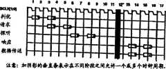
图3是一个时序图,依据一个实施例说明了用于两个示例事务的示例总线事务阶段关系。在上面显示了总线时钟(BCLK[1:0])的周期(1,2,3,4,...17)。具有一个数字1的矩形指示用于事务1的各个阶段,而具有一个数字2的矩形指示用于事务2的阶段。能够从图3中看出,以一种流水线方式提供事务。例如,对事务1来说,判优发生在总线时钟周期1和2中,请求发生在周期3和4中,探听发生在周期6和7中,而且响应和数据传送发生在周期13和14中。因此,能够看出在初始请求阶段之后一个响应和数据传送可以发生许多个总线时钟周期。此外,在不同事务的阶段之间能有重叠。例如,用于事务2的判优阶段与用于事务1的请求阶段大约同时发生。Figure 3 is a timing diagram illustrating example bus transaction phase relationships for two example transactions, according to one embodiment. The periods (1, 2, 3, 4, ... 17) of the bus clock (BCLK[1:0]) are shown above. Rectangles with a
V.信号模式V. Signal Mode
依据一个实施例,处理器总线117是可扩展的,并且支持两种信号模式。第一种是一个公共时钟信号模式,在该模式下所有的信号激活和采样或者锁存点相对于一个公共总线时钟(BCLK#)发生,其中该公共总线时钟(BCLK#)是在所有代理之间连续提供的。总线时钟通常由在一个母板上提供的一个时钟芯片或者时钟电路产生,并且对在一台计算机中的所有处理器或者代理是共用的。相对于公共总线时钟的信号计时被称为公共时钟(1X)信号模式。依据一个实施例,经由控制总线提供的许多控制信号使用该公共时钟(1X)信号模式进行传送。According to one embodiment, processor bus 117 is scalable and supports two signaling modes. The first is a common clock signaling mode in which all signal activation and sampling or latching points occur relative to a common bus clock (BCLK#) that is clocked between all agents provided continuously. The bus clock is usually generated by a clock chip or clock circuit provided on a motherboard and is common to all processors or agents in a computer. Signal timing relative to the common bus clock is referred to as common clock (1X) signaling mode. According to one embodiment, a number of control signals provided via the control bus are transmitted using this common clock (1X) signal pattern.
第二种信号模式是一个多重抽吸信号模式,它允许一个由公共时钟信号模式支持的传输速度倍数的信息传输速度。因此,依据一个实施例,多重抽吸信号模式能够支持以公共(即系统)总线时钟频率倍数的速度、在代理之间经由处理器总线117传输信息。例如,多重抽吸信号模式可以提供例如一个双重抽吸信号模式,或是可以提供一个四重抽吸信号模式,其中双重抽吸信号模式允许信息(例如,数据,地址或者其他信息)以公共时钟频率速度的两倍(2X)进行传输,而四重抽吸信号模式以总线时钟频率的四倍(4X)提供信息传输。为了便于以这样大于公共总线时钟的速度或者频率传输信息,驱动代理还发布或者提供一个被称为时序“选通脉冲”的伴生信号,该信号由接收器使用作为一个参考用于捕获或者锁存该多重抽吸的信息。The second signaling mode is a multiple-pump signaling mode that allows an information transfer rate that is a multiple of the transfer rate supported by the common clock signaling mode. Thus, according to one embodiment, the multi-pump signaling mode can support the transfer of information between agents via the processor bus 117 at speeds that are multiples of the common (ie, system) bus clock frequency. For example, the multi-pumped signaling mode may provide, for example, a double-pumped signaling mode, or may provide a quadruple-pumped signaling mode, where the double-pumped signaling mode allows information (eg, data, address, or other information) to be clocked on a common clock The clock speed is twice (2X) for transfers, while the quad-pumped signaling mode provides information transfers at four times (4X) the bus clock frequency. To facilitate the transfer of information at such a speed or frequency greater than the common bus clock, the driving agent also issues or provides an accompanying signal called a timing "strobe" that is used by the receiver as a reference for capturing or latching Information about the multiple puffs.
术语“断定”是指一个信号被驱动到它的有效电平(即,对一个低电平有效的信号来说,被驱动到零),而且术语“取消断定”是指信号被驱动到它的无效电平。在如下所述的某些时序图中使用了正方形、圆形和三角形符号以指示特定信号何时被驱动或者采样。正方形指示一个信号在那个时钟周期中被驱动(断定,启动)。圆形指示一个信号在那个时钟周期中被采样(观察,锁存)。圆形通常被用来在公共时钟(1X)信号模式中基于总线时钟(BCLK)的一个上升(或者下降)沿显示一个采样点。三角形指示一个信号基于被称为“选通脉冲”的一个伴生信号的一个上升或者下降沿被采样或者捕获。选通脉冲最好可以是仅仅在信息(例如,数据、地址、其它信息)传送期间内经由处理器总线通常在多重抽吸模式下被打开或者被激活。The term "asserted" means that a signal is driven to its active level (that is, driven to zero for an active-low signal), and the term "deasserted" means that the signal is driven to its invalid level. Square, circle, and triangle symbols are used in some of the timing diagrams described below to indicate when a particular signal is driven or sampled. A square indicates that a signal is driven (asserted, enabled) during that clock cycle. Circles indicate in which clock cycle a signal is sampled (observed, latched). Circles are usually used to display a sample point based on a rising (or falling) edge of the bus clock (BCLK) in common clock (1X) signaling mode. A triangle indicates that a signal is sampled or captured based on a rising or falling edge of an accompanying signal called a "strobe". The strobe may preferably be turned on or activated via the processor bus, typically in multipump mode, only during information (eg, data, address, other information) transfers.
A.公共时钟信号模式A. Common clock signal mode
依据公共时钟(1X)信号模式的一个实施例,在处理器总线117上的所有代理被要求驱动它们的有效输出并且采样所需的输入。依据一个实施例,每个输入应该在总线时钟的上升沿上在一个有效采样间隔期间内被采样,而且一到下一个总线时钟沿上升就把它的效果或者结果向外驱动到总线117上。这个方法实例允许一个完整的总线时钟周期用于组件间的通信(信号传输和传播),以及在接收器处允许至少一个完整的总线时钟周期来解释这些信号并且计算和输出一个响应。因此,在一个代理在一个或多个总线时钟周期中把数据驱动到处理器总线上之后,在另一个代理能够驱动处理器总线117之前有一个总线时钟周期的暂停(例如,一个不工作周期或者不活动周期)。According to one embodiment of a common clock (1X) signaling mode, all agents on the processor bus 117 are required to drive their active outputs and sample required inputs. According to one embodiment, each input should be sampled during an active sampling interval on the rising edge of the bus clock and have its effect or result driven out onto the bus 117 as soon as the next rising edge of the bus clock rises. This method instance allows one full bus clock cycle for inter-component communication (signal transmission and propagation), and at least one full bus clock cycle at the receiver to interpret the signals and compute and output a response. Thus, after one agent drives data onto the processor bus for one or more bus clock cycles, there is a bus clock cycle pause (e.g., a period of inactivity or periods of inactivity).
图4是一个示例时序图,依据一个实施例说明了公共时钟(1X)信号模式的示例操作。当信号出现在处理器总线117上时显示该信号。显示了总线时钟(BCLK)的四个周期。还显示了两个额外的示例信号,包括A#和B#,它们可以是任何类型的信号。例如,A#可以是来自于第一代理的一个第一控制信号,而B#可以是来自于第二代理的一个第二信号。第一和第二控制信号可以被提供作为一个例如信号交换或者总线协议的一部分。FIG. 4 is an example timing diagram illustrating example operation of a common clock (1X) signal mode, according to one embodiment. Signals are displayed as they appear on processor bus 117 . Four cycles of the bus clock (BCLK) are shown. Also shown are two additional example signals, including A# and B#, which could be any type of signal. For example, A# could be a first control signal from a first agent, and B# could be a second signal from a second agent. The first and second control signals may be provided as part of, for example, a handshake or bus protocol.
如图1所示,信号A#在时钟周期1的上升沿(如在A#中的正方形所示)处被驱动(或者断定),并且在总线时钟周期2开始处的一个上升沿在该接收器处被锁存(如用于A#的圆圈所示)。因此,提供了时钟周期1用于信号传播。虽然A#在周期1的开始处被断定,但是它没有在该总线上被观察直到周期2的开始为止。然后,存在一个暂停或者不活动的时钟周期(在用于逻辑延迟和用于接收器解释该信号的总线时钟周期2期间)。该接收器然后在总线时钟周期3的开始处驱动或者断定B#信号(如用于B#的正方形所示),其在周期4的开始处由另一个代理观察和捕获(如用于B#的圆圈所示)。As shown in Figure 1, signal A# is driven (or asserted) at the rising edge of clock cycle 1 (as indicated by the square in A#), and a rising edge at the beginning of
依据一个实施例,一个处理器包含一个64字节的高速缓存线(而不是在某些奔腾处理器中使用的32字节高速缓存线)。因此,如果数据使用公共时钟(1X)信号模式和64条数据总线线传输,则64字节(一个高速缓存线)的数据能够在8个总线时钟周期内被驱动或者传输。然而,在许多应用中,有可能期望提供一个更快的数据传送率或者更大的带宽。According to one embodiment, a processor contains a 64-byte cache line (instead of the 32-byte cache line used in some Pentium processors). Therefore, if data is transferred using a common clock (1X) signaling pattern and 64 data bus lines, 64 bytes (one cache line) of data can be driven or transferred in 8 bus clock cycles. However, in many applications it may be desirable to provide a faster data transfer rate or greater bandwidth.
B.多重抽吸信号模式B. Multiple suction signal mode
在许多实例中,处理器总线长度117、电限制(包含用于穿过总线的信号传播等待时间)可以阻止增加处理器总线频率。因此,依据一个实施例,而不是增加处理器总线时钟频率,该多重抽吸信号协议通过以该总线时钟(BCLK)频率的一个倍数操作适当的总线信号组(例如,地址总线或者数据总线)来增加该数据传送率(经由该公共时钟信号模式)。In many instances, processor bus length 117, electrical limitations, including latency for signal propagation across the bus, may prevent increasing processor bus frequency. Therefore, in accordance with one embodiment, rather than increasing the processor bus clock frequency, the multiple-pump signaling protocol operates by operating the appropriate set of bus signals (eg, address bus or data bus) at a multiple of the bus clock (BCLK) frequency. Increase the data transfer rate (via the common clock signal mode).
1.一个四重抽吸信号模式的示例1. Example of a quadruple pumping signal pattern
在该四重抽吸信号模式中,该适当的总线信号组以该总线时钟(BCLK)频率的四倍(4X)进行操作。换句话说,在四重抽吸信号模式中,在一个总线时钟周期内(这是它在该公共时钟或者1X信号模式中驱动一个信息单元所需的时间)四个信息单元被驱动到该处理器总线117上。In the quad pumped signal mode, the appropriate set of bus signals operates at four times (4X) the frequency of the bus clock (BCLK). In other words, in quad pumped signaling mode, four information units are driven to the process during one bus clock cycle (which is the time it takes to drive one information unit in the common clock or 1X signaling mode) device bus 117.
图5是一个时序图,依据一个实施例说明了一个示例四重抽吸信号模式。虽然该四重抽吸信号模式能用于任何类型的信号,但是依据一个示例实施例,该四重抽吸信号协议用于传送数据。在图5中的显示了两个总线时钟周期和第三总线时钟周期的一部分。穿过该处理器总线117的传输时间(或者信号传播时间)的最坏情况是这样的,即在第一个信息单元已经锁存在该接收器处(接收代理)之前,第二个信息单元可以被驱动到在该驱动器处的处理器总线117上(即,该代理驱动信息到该处理器总线上)。FIG. 5 is a timing diagram illustrating an example quadruple pumping signal pattern, according to one embodiment. Although the quadruple-pumped signaling mode can be used for any type of signal, according to an example embodiment, the quadruple-pumped signaling protocol is used to transmit data. In Figure 5 two bus clock cycles and part of a third bus clock cycle are shown. The worst-case transmission time (or signal propagation time) across the processor bus 117 is such that a second information unit can is driven onto the processor bus 117 at the driver (ie, the agent drives information onto the processor bus).
依据一个实施例,该驱动器(或者驱动代理)在该总线时钟(BCLK)周期的上升沿、以及该25%、50%和75%点发送或者驱动一个新的信息单元到该上升沿上。According to one embodiment, the driver (or driver agent) sends or drives a new information element on the rising edge of the bus clock (BCLK) cycle, and the 25%, 50% and 75% points.
该接收器也发送一个被称为数据选通脉冲信号的伴生定时信号来指示何时该接收器应当采样或者捕获该数据。该选通信号更可取地是只有当信息使用该多重抽吸信号模式发送时才被发送或者驱动(激活)。The receiver also sends an accompanying timing signal called a data strobe signal to indicate when the receiver should sample or capture the data. The strobe signal is preferably sent or driven (activated) only when information is sent using the multiple pump signal mode.
因为该数据和选通信号由同一个驱动器或者源产生,该数据和选通脉冲将具有相同的路径。结果,该选通信号和数据信号应当具有相同的路径,因此具有大致相同的延迟。因此,由同时发送一个选通脉冲和数据的驱动器或者源实现的一个有利条件是,该数据信号和该选通信号将同阶段(或者同步)到达在每个在该总线117上的代理处。因此,这个一个驱动器即发送数据又发送一个时序选通信号的技术能够被称为是一个源同步传送。在该四重抽吸信号模式中,在每个总线时钟周期中应该有四个数据选通脉冲(例如,四个时序选通脉冲边沿),每一个用于四个数据单元中的一个。不幸地时,在以比较高的频率产生一个选通信号中可能出现问题。在高时钟频率处,在该上升沿比率和该下降沿比率之间的差别能够是重要的。此外,可能难以提供一个具有50%作业周期的时钟信号或者选通信号。结果,在某些高时钟频率处,该选通信号的上升沿和下降沿将不会用来标识采样点,因为这个可能产生不对称或者引入一定程度的时序不准。相反地,仅仅使用该选通脉冲两个边沿的一个(即,仅仅使用该选通信号的上升沿或者仅仅下降沿来采样或者捕获该四重抽吸数据)来获得更对称或者更统一的选通脉冲时序或者采样间隔可能是有利的。Since the data and strobe signals are generated by the same driver or source, the data and strobe pulses will have the same path. As a result, the strobe signal and the data signal should have the same path and therefore approximately the same delay. Thus, an advantage realized by a driver or source that simultaneously sends a strobe and data is that the data signal and the strobe signal will arrive at each agent on the bus 117 in phase (or synchronously). Therefore, this technique where one driver sends both data and a timing strobe signal can be called a source synchronous transfer. In the quad pumped signaling mode, there should be four data strobes (eg, four timing strobe edges) in each bus clock cycle, one for each of the four data cells. Unfortunately, problems can arise in generating a strobe signal at relatively high frequencies. At high clock frequencies, the difference between the rising edge ratio and the falling edge ratio can be significant. Additionally, it may be difficult to provide a clock signal or strobe signal with a 50% duty cycle. As a result, at certain high clock frequencies, the rising and falling edges of the strobe signal will not be used to identify sample points, as this may create asymmetry or introduce a degree of timing inaccuracy. Conversely, using only one of the two edges of the strobe (i.e., using only the rising edge or only the falling edge of the strobe signal to sample or capture the quadruple pumped data) achieves a more symmetrical or uniform selection. Pulse timing or sampling intervals may be advantageous.
如果仅仅使用了该选通脉冲的一个边沿,则这个一般将要求一个是该总线时钟频率倍数的时钟频率。在四重抽吸数据(每个总线时钟周期四个数据单元)的情况下,如果仅仅一个边沿用于时序则该选通信号频率应当是该总线时钟频率的四倍(4X)。If only one edge of the strobe is used, this will generally require a clock frequency that is a multiple of the bus clock frequency. In the case of quadruple pumped data (four data units per bus clock cycle), the strobe frequency should be four times (4X) the bus clock frequency if only one edge is used for timing.
不幸地是,如果该处理器时钟频率是100兆赫(举例来说),则这将要求一个是400兆赫的选通信号频率(在这个示例中)。然而,一个是该总线时钟频率四倍的选通信号频率可能遇到不同于该发送数据或者信息的延迟,这能够在该接收器处影响该数据和选通脉冲的对齐。一种在传送的选通信号和传送的数据之间的未对准可能导致该接收器捕获坏的或者错误的数据。此外,在这样高的频率(例如400兆赫)处,信号衰减能够是非常高的。Unfortunately, if the processor clock frequency is 100 MHz (for example), this would require a strobe frequency of 400 MHz (in this example). However, a strobe frequency that is four times the bus clock frequency may experience a different delay than the transmitted data or information, which can affect the alignment of the data and strobes at the receiver. A misalignment between the transmitted strobe signal and the transmitted data may cause the receiver to capture bad or erroneous data. Furthermore, at such high frequencies (eg 400 MHz) the signal attenuation can be very high.
因此,依据一个实施例,多个数据选通信号用于在每个总线时钟周期提供四个选通脉冲,而不用使用一个是该总线时钟频率四倍(4X)的一个选通脉冲频率。依据一个实施例,在该总线时钟频率两倍处分别提供两个数据选通信号(DSTBp#和DSTBn#)。因此,如果该总线时钟频率是100兆赫,则当由该驱动器(或者驱动代理)激活或者产生时,两个数据选通信号每个都将具有一个200兆赫的频率。做为选择,能够使用四个数据选通信号(当激活时,每个和该总线时钟相同的频率),其每个选通信号都在每个总线时钟周期中提供一个选通脉冲或者下降沿。Thus, according to one embodiment, multiple data strobe signals are used to provide four strobes per bus clock cycle instead of using a strobe frequency that is four times (4X) the bus clock frequency. According to one embodiment, two data strobe signals (DSTBp# and DSTBn#) are respectively provided at twice the bus clock frequency. Thus, if the bus clock frequency is 100 MHz, the two data strobe signals will each have a frequency of 200 MHz when activated or generated by the driver (or driver agent). Alternatively, four data strobes (each at the same frequency as the bus clock when active) can be used, each of which provides a strobe or falling edge every bus clock cycle .
再次参考图5的时序图,该驱动器在总线时钟周期1的上升沿、以及25%、50%和75%点上发送或者驱动一个新的信息或者数据单元。被标志为D1、D2、D3和D4的数据单元用于在这个示例中的四个数据单元。这个实施例还使用两个数据选通信号、包括DSTBp#和DSTBn#。依据一个实施例,这两个数据选通信号是彼此异相(或者以一种交错或者偏移方案)产生的。这允许一个选通信号中来标识用于奇数数据单元(例如,D1、D3、D5...)的采样点,而另一个选通信号用于偶数数据单元(例如、D2、D4、D6,..)。Referring again to the timing diagram of FIG. 5, the driver transmits or drives a new message or data unit at the rising edge of
虽然在图5的示例中仅仅显示了两个选通信号,但是任意数量的选通信号可用于标识用于一个源同步传送数据的采样点。如上所述,提供多个选通信号以便该选通信号两个边沿中的仅仅一个可用于标识采样点(或者选通脉冲)而同时降低该选通信号的频率,是尤其有利的。举例来说,如果使用了一个6X抽吸协议(而不是四重抽吸),能够使用三个选通信号,其中所有三个选通信号能够被类似地偏移或者交错,以便选通脉冲1能够用于数据单元D1和D4,选通脉冲2用于数据单元D2和D5,而选通脉冲3用于数据单元D3和D6,等。Although only two strobes are shown in the example of FIG. 5, any number of strobes may be used to identify sampling points for one source synchronously transferred data. As mentioned above, it is especially advantageous to provide multiple strobe signals such that only one of the two edges of the strobe signal can be used to identify a sample point (or strobe pulse) while at the same time reducing the frequency of the strobe signal. For example, if a 6X pumping protocol is used (instead of quadruple pumping), three strobes can be used, where all three strobes can be similarly shifted or interleaved so that
依据一个实施例,该选通信号两个边沿中的仅仅一个用于标识或者同步数据采样点。在这个特定实施例中,仅仅该两个数据选通信号的下降沿用来标识用于采样该信息或者数据的点。该数据选通脉冲(或者该数据选通信号的下降沿)在四个信息或者数据单元每一个的中心。因此,该数据选通信号的四个下降沿(或者选通脉冲)将在该总线时钟(BCLK)周期的12.5%、37.5%、62.5%和87.5%点上发生。因此,这两个选通信号提供等间隔的选通脉冲或者下降沿。According to one embodiment, only one of the two edges of the strobe signal is used to identify or synchronize data sampling points. In this particular embodiment, only the falling edges of the two data strobe signals are used to identify points for sampling the information or data. The data strobe (or the falling edge of the data strobe signal) is centered in each of the four information or data cells. Thus, the four falling edges (or strobes) of the data strobe signal will occur at points 12.5%, 37.5%, 62.5%, and 87.5% of the bus clock (BCLK) period. Therefore, the two strobe signals provide equally spaced strobe pulses or falling edges.
如图5所示,在总线时钟周期1开始处,一个DRDY#被驱动到总线117上(如用于DRDY#的正方形所示)。DRDY#指示有效数据已经放置在处理器总线117上并且必须被采样或者锁存。第一个数据单元(D1)在总线时钟周期1的上升沿处(如用于D#(@driver)的第一个矩形所示)被该驱动器驱动到处理器总线117上。第一个数据选通信号(DSTBp#)然后由该驱动器在第一个总线时钟周期的12.5%点处激活,如在DSTBp#(@driver)中的第一个正方形所示。因此,该用于第一个数据单元(D1)的选通脉冲(或者下降沿)置于第一个数据单元的中心。一旦一个选通信号已经被激活或者打开了,它一般继续激活直到数据已经驱动到总线上为止。As shown in FIG. 5, at the beginning of
此外,一个第二数据单元由该驱动器在该总线时钟周期1的25%点处驱动,如用于D#(@driver)的第二个矩形所示。第二个数据选通信号(DSTBn#)在该总线时钟周期1的37.5%点处被激活并且提供一个置于第二个数据单元(D2)中心的下降沿(或者选通脉冲)。Additionally, a second data unit is driven by the driver at the 25% point of
同样地,第三和第四数据单元(分别为D3和D4)在总线时钟周期1的50%点和75%点处被驱动。相应的数据选通脉冲(该数据选通信号的下降沿)由该驱动器在62.5%点(由该DSTBp#选通信号)和87.5%点(由该DSTBn#选通信号)处提供或者驱动。因为该数据选通信号由一个是该总线时钟频率两倍(2X)的频率提供,每个数据选通信号每1/2个总线时钟周期将提供一个选通脉冲或者下降沿。因此,该DSTBp#选通信号在该总线时钟周期的12.5%和62.5%点处提供下降沿或者选通脉冲,而DSTBp#选通信号在该总线时钟周期的37.5%和87.5%点处提供下降沿或者选通脉冲。因此,能够看出这两个数据选通信号(DSTBp#和DSTBn#-)是彼此交错或者不同相的。这允许交替选通信号以每四分之一个总线时钟周期(在两个数据选通信号之间)就提供一个下降沿(或者选通脉冲)。这提供了每总线时钟周期四个选通脉冲或者下降沿,用于每个总线时钟周期标识四个数据单元的采样或者捕获点,同时降低每个选通脉冲的频率。此外,因为同一个边沿(在这个示例中为下降沿)用于在每个数据选通信号中的选通脉冲,时序和电路被简化了。Likewise, the third and fourth data elements (D3 and D4, respectively) are driven at the 50% and 75% points of
依据一个实施例,为了确保正确操作,信息从该驱动代理传递到任何接收器的等待时间应当小于或等于一个总线时钟减于该输入锁存器的准备时间。这将避免,如果该接收器在下一个阶段期间变为总线所有者,在用于后续数据阶段的数据线上的竞争。According to one embodiment, to ensure correct operation, the latency of information transfer from the driving agent to any receiver should be less than or equal to one bus clock minus the setup time of the input latch. This will avoid contention on the data line for the subsequent data phase if the receiver becomes the bus owner during the next phase.
图5还显示了在该接收器处的数据捕获。在该信号(数据和数据选通脉冲)由该驱动器驱动之后,这些信号沿着处理器总线117向下传送并且到达该目标或者接收器。第一个数据单元在接收器处接收,如D#(@receiver)信号所示。第一个数据单元(D1)在第一个选通脉冲上被采样或者捕获,其为DSTBp#(@receiver)的第一个下降沿。用于该DSTBp#(@receiver)的第一个三角形标识用于采样或者捕获第一个数据单元的选通脉冲或者点,而用于DSTBp#(@receiver)的第二个三角形标识用于在该接收器处采样该第三个数据单元的点或者选通脉冲。类似地,用于第二个数据选通信号(DSTBn#(@receiver))的两个三角形标识用于让该接收器采样或者捕获第二和第四个数据单元(D2、D4)的点。Figure 5 also shows the data capture at the receiver. After the signals (data and data strobes) are driven by the driver, the signals travel down the processor bus 117 and to the target or receiver. The first data unit is received at the receiver, as indicated by the D# (@receiver) signal. The first data unit (D1) is sampled or captured on the first strobe, which is the first falling edge of DSTBp#(@receiver). The first triangle for this DSTBp#(@receiver) marks the strobe or point at which the first data unit is sampled or captured, while the second triangle for the DSTBp#(@receiver) is used for the The point or strobe at which the third data unit is sampled at the receiver. Similarly, the two triangles for the second data strobe signal (DSTBn#(@receiver)) identify points for the receiver to sample or capture the second and fourth data units (D2, D4).
如图5所示,第一个数据单元D1可以在时钟2开始处的上升沿之后,以及在时钟周期2(下一个时钟周期)的12.5%点处被采样或者捕获(选通)到该接收器中。(如在这里使用的那样,术语“捕获”、“采样”和“锁存”被泛泛地使用以意指大致相同的事情)。然而,用于所有数据单元的数据没有被锁存到该接收器里,直到总线时钟周期3的上升沿为止。因此,虽然在接近总线时钟周期2开始处接收和捕获数据单元D1,但是所有数据对于接收器都是不可用的,直到总线时钟周期3开始为止。该接收代理更可取地是包括一个足够存储八个数据单元的FIFO(先进先出)缓存。这八个数据单元FIFO足够大来存储一次数据传送的四个单元以及用于下一次传送的下一个四个单元。这允许四个新的数据单元被接收和捕获,同时前四个数据单元正从该FIFO弹出或者锁存到接收器中。它的净效果是该公共时钟信号模式带宽的四倍,并且具有增加的、用于在该接收器或者设备内部锁存的第一个信号群的等待时间的效果。As shown in Figure 5, the first data unit D1 can be sampled or captured (gated) into the receive device. (As used herein, the terms "capture," "sample," and "latch" are used loosely to mean substantially the same thing). However, data for all data cells is not latched into the receiver until the rising edge of
此外,依据一个实施例,多条线用来运载两个数据选通信号每一个的多个拷贝(DSTBp#和DSTBn#)。依据一个实施例,有四个DSTBn#信号和四个DSTBp#信号,如在以下表格中表示的那样。Furthermore, according to one embodiment, multiple lines are used to carry multiple copies of each of the two data strobe signals (DSTBp# and DSTBn#). According to one embodiment, there are four DSTBn# signals and four DSTBp# signals, as represented in the table below.
数据选通脉冲有效区的示例实施例
这四个DSTBp#信号逻辑上是相同的,四个DSTBn#信号也是如此,但是每一个数据选通信号物理上用该请求信号的一个子集(即,该数据线的一个子集)路由以减少在数据和数据选通信号之间的计时变形或者不一致。The four DSTBp# signals are logically identical, as are the four DSTBn# signals, but each data strobe signal is physically routed with a subset of the request signals (i.e., a subset of the data lines) to Reduce timing distortion or inconsistency between data and data strobe signals.
图8是依据一个实施例、用于在代理之间传输信息的一个装置的框图。第一个总线代理802连接到第二个总线代理832。第一个总线代理802包含一个数据选通脉冲发生器1/接收器1,用于经由第一个双向数据选通信号线820产生和接收第一个数据选通信号(例如,DSTBp#);以及一个数据选通脉冲发生器2/接收器2用于经由第二个双向数据选通信号线822产生和接收第二个数据选通信号(例如,DSTBn#)。总线代理802还包含一个总线收发器806,该总线收发器806包含一个传送电路用于传送或者驱动数据信号到数据总线或者数据信号线826上,以及一个接收电路用于接收经由该数据信号线826接收的数据信号。第二个总线代理832类似地包含一个数据选通脉冲发生器1和一个数据选通脉冲发生器2用于分别产生两个数据选通信号到数据选通信号线820和822上。一个公共(或者系统)总线时钟发生器810提供该公共或者系统总线时钟到总线代理802和832。Figure 8 is a block diagram of an apparatus for transferring information between agents, according to one embodiment. The first bus agent 802 is connected to the second bus agent 832 . The first bus agent 802 includes a
2.把地址总线速度和数据总线相匹配2. Match the address bus speed with the data bus
依据一个实施例,该高速缓存线尺寸已经增加到64个字节(在某些奔腾处理器中的高速缓存线是32个字节)。因此,使用该四重抽吸信号协议和具有64条数据线的数据总线宽度,一条高速缓存线(或者64个字节)能够在两个总线时钟周期中传送或者传输:64个字节=(2个周期)×(4抽吸/周期)(每抽吸8个字节)。According to one embodiment, the cache line size has been increased to 64 bytes (cache lines in some Pentium processors are 32 bytes). Thus, using the quad pumped signaling protocol and a data bus width of 64 data lines, one cache line (or 64 bytes) can be transferred or transferred in two bus clock cycles: 64 bytes = ( 2 cycles) x (4 pumps/cycle) (8 bytes per pump).
然而,在某些奔腾处理器中,一个请求(包含一个地址)在三个总线时钟周期中传送。用于某些奔腾处理器请求阶段的三个总线时钟周期包含下列:However, in some Pentium processors, a request (including an address) is transferred in three bus clock cycles. The three bus clock cycles used in the request phase of some Pentium processors include the following:
周期1-子阶段a-地址(经由地址总线提供),以及一种类型请求(例如,读,写)。Cycle 1 - subphase a - address (provided via address bus), and a type of request (eg, read, write).
周期2-子阶段b-该请求的辅助详细信息,包括字节使能、长度等(经由地址线或者地址总线提供)。Cycle 2 - Subphase b - Ancillary details of the request, including byte enables, length, etc. (provided via address lines or address bus).
周期3-一个不工作周期或者往返周期,其允许在该总线上的信号变为静止,以允许另一个代理驱动该总线。Cycle 3 - A dead cycle or round trip cycle that allows the signal on the bus to go quiet to allow another agent to drive the bus.
因此,依据一个实施例,一个高速缓存线能够在两个总线时钟周期中经由该数据总线传选。然而,在某些奔腾处理器中,地址和请求时序要求三个总线时钟周期用于传送一个请求。因此,在某些奔腾处理器中,地址总线时序或者带宽不匹配在上述实施例(看到图5)中描述的、改进的四重抽吸数据总线的速度。一个更缺乏和更有价值的资源是该数据总线宽度和数据总线带宽。因此,依据一个实施例,更可取的是让该数据总线带宽压制或者限制处理器总线,而不是地址总线带宽。因此,为了防止地址总线减速或者压制该处理器总线,期望调整在地址总线上的地址和请求时序以至少匹配该数据总线的带宽或者速度(在这个示例中,用于在该数据总线上传输一个高速缓存线)。Thus, according to one embodiment, a cache line can be selected via the data bus in two bus clock cycles. However, in some Pentium processors, address and request timing requires three bus clock cycles to transmit a request. Therefore, in some Pentium processors, the address bus timing or bandwidth does not match the speed of the improved quad-pumped data bus described in the above embodiment (see FIG. 5). A scarcer and more valuable resource is the data bus width and data bus bandwidth. Therefore, according to one embodiment, it is preferable to have the data bus bandwidth overwhelm or limit the processor bus rather than the address bus bandwidth. Therefore, in order to prevent the address bus from slowing down or overwhelming the processor bus, it is desirable to adjust address and request timing on the address bus to at least match the bandwidth or speed of the data bus (in this example, the data bus used to transmit a cache line).
因此,依据一个实施例,该经由地址总线提供的、请求阶段的时序和速度被调整为匹配该数据总线的整体速度。保持该不工作周期或者往返周期是合符需要的。因此,依据一个示例实施例,地址总线被双重抽吸以在一个总线时钟周期中提供两个信息单元(请求的子阶段a和子阶段b)。Thus, according to one embodiment, the timing and speed of the request phase provided via the address bus is adjusted to match the overall speed of the data bus. It is desirable to maintain this off-duty or round-trip period. Thus, according to an example embodiment, the address bus is double pumped to provide two information units (requested subphase a and subphase b) in one bus clock cycle.
3.一个双重抽吸信号模式的示例3. An example of a dual pumping signal pattern
通常,依据一个实施例,一个该双重抽吸信号模式中以该总线时钟(BCLK)频率的两倍(2X)操作该适当的总线信号组。图6是一个时序图,依据一个实施例说明了一个示例双重抽吸信号模式例子。虽然任何信号都可以是双重抽吸的,但是在这个实施例中地址总线是双重抽吸的。Typically, according to one embodiment, the appropriate set of bus signals is operated at twice (2X) the frequency of the bus clock (BCLK) in a double-pumped signal mode. FIG. 6 is a timing diagram illustrating an example dual pumping signal mode example in accordance with one embodiment. Although any signal can be double pumped, in this embodiment the address bus is double pumped.
参考图6,该ADS#信号在请求阶段开始处变低。在该双重抽吸信号模式中,以它使用该公共时钟信号模式驱动一个单元所花费的时间(即,在一个总线时钟周期期间),把两个信息单元驱动到总线上。由于传输时间(或者在该处理器总线117上的信号传播时间)可以在第一个单元被锁存在接收器(或者多个)处之前在该驱动器处驱动第二个信号群或者信息单元。依据一个实施例,该驱动器在该总线时钟周期的上升沿和50%点上发送一个新的信息单元。Referring to Figure 6, the ADS# signal goes low at the beginning of the request phase. In the double pumped signaling mode, two information cells are driven onto the bus for the time it takes to drive one cell using the common clock signal mode (ie, during one bus clock cycle). Due to transmission time (or signal propagation time on the processor bus 117 ) a second signal group or information unit may be driven at the driver before the first unit is latched at the receiver(s). According to one embodiment, the driver sends a new information element on the rising edge and the 50% point of the bus clock cycle.
如图6所示,在总线时钟周期1开始处的下降沿开始的第一半总线时钟周期1上发送提供事务地址的请求子阶段a(Aa)。在从总线时钟周期1的50%点开始的第二半总线时钟周期1上发送提供用于该事务的某些辅助详细信息的、该请求子阶段b(Ab)。在图6中这两个信息单元显示为用于A#(@driver)线的Aa和Ab的两个矩形(Aa指示经由地址线提供的、该请求的子阶段a,而Ab指示经由地址线提供的、该请求的子阶段b)。因此,因为两个信息单元(Aa和Ab)在一个总线时钟周期期间被传送或者发送,所以地址总线是双重抽吸的。As shown in FIG. 6 , the request subphase a (Aa) providing the transaction address is sent on the first half of
此外,因为用于该请求的信息将使用一个双重抽吸信号模式发送(每一总线时钟周期两个信息单元),所以该信息更可取地是从一个源同步传送发送。因此,除了这两个信息单元之外,该驱动器还驱动或者激活一个地址选通信号,来每一个总线时钟周期(当激活时)提供两个地址选通脉冲。地址选通脉冲提供或者标识用于采样在地址总线上发送的这两个信息单元(Aa和Ab)的点。Also, since the information for the request will be sent using a double-pumped signaling mode (two information elements per bus clock cycle), the information is preferably sent from a source synchronous transfer. Therefore, in addition to these two information elements, the driver also drives or activates an address strobe signal to provide two address strobes per bus clock cycle (when active). The address strobe provides or identifies the point for sampling the two information units (Aa and Ab) sent on the address bus.
依据一个实施例,使用的一个地址选通信号(ADSTB#)与总线时钟(BCLK)具有相同的频率。然而,为了在一个总线时钟周期期间提供两个选通脉冲,地址选通信号的下降沿和上升沿都将被用作选通脉冲或者标识用于这两个经由地址总线提供的信息单元的采样点。如图6所示,该驱动器在总线时钟周期1的25%点处激活一个地址选通信号(ADSTB#),这是在信息单元1(Aa)的中心时刻。依据一个实施例,用于第一个信息单元的地址选通脉冲(Aa或者该请求的子阶段a)被提供为该ADSTB#信号的下降沿(在总线时钟周期1的25%点处驱动),而用于第二信息单元(Ab或者请求的子阶段b)的地址选通脉冲被提供为该ADSTB#信号的上升沿(在总线时钟周期的75%点处驱动)。According to one embodiment, an address strobe signal (ADSTB#) is used having the same frequency as the bus clock (BCLK). However, in order to provide two strobes during one bus clock cycle, both the falling and rising edges of the address strobe signal will be used as strobes or to identify samples for the two elements of information provided via the address bus. point. As shown in FIG. 6, the driver activates an address strobe signal (ADSTB#) at the 25% point of
即使地址选通脉冲具有一个与总线时钟相同的频率,但是该总线时钟将不会被用作用于该信息单元的选通信号,因为该总线时钟信号在适当时间不提供上升和下降沿。此外,该总线时钟信号总是激活的(与一个选通信号仅仅在一个源同步传送期间被激活相反)。地址选通信号用来提供选通脉冲用于这两个信息单元的脉冲或者采样点,是因为该地址选通信号能够被激活(打开)和取消激活(关闭)而不管总线时钟的状态或者阶段。通过让该从同一个源驱动的选通脉冲作为信息,在这选通脉冲中的延迟匹配在该信息中的延迟,由此允许同时有多于一位在一条线上。Even though the address strobe has a frequency the same as the bus clock, the bus clock will not be used as a strobe signal for the information element because the bus clock signal does not provide rising and falling edges at the proper times. Furthermore, the bus clock signal is always active (as opposed to a strobe signal which is only active during a source synchronous transfer). The address strobe signal is used to provide strobe pulses or sampling points for these two information elements because the address strobe signal can be activated (on) and deactivated (off) regardless of the state or phase of the bus clock . By having the strobe driven from the same source as the information, the delay in the strobe matches the delay in the information, thereby allowing more than one bit to be on a line at the same time.
该信息单元(Aa和Ab)以及地址选通信号沿着处理器总线117传送并且在总线时钟周期2开始处到达接收器。如图6所示,第一个信息单元(Aa)在该ADSTB#(@receiver)信号的下降沿上被捕获或者采样,而且第二个信息单元在该ADSTB#(@receiver)信号的上升沿被捕获或者采样,如在该ADSTB#(@receiver)信号上的两个三角形所示。因此,能够看出,当该数据是有效(并且应当被捕获)时,该接收器基于来自该驱动器的一个指示确定性地捕获该数据或者信息。The information elements (Aa and Ab) and the address strobe signal travel along the processor bus 117 and arrive at the receiver at the beginning of
依据一个实施例,数据从该驱动代理传送到任何接收器的等待时间应当小于或等于一个总线时钟周期减于该输入锁存器的准备时间。如果该接收器变为下一个阶段的所有者的话,这将会避免在用于第二个或者后续阶段的地址线(或者地址总线)及其他线上的竞争。它的净效果是该公共时钟信号模式带宽的两倍,并且具有增加的、用于在该组件或者接收器内部锁存的第一个信号群的等待时间的效果。According to one embodiment, the latency of data transfer from the driving agent to any receiver should be less than or equal to one bus clock cycle minus the setup time of the input latch. This will avoid contention on the address line (or address bus) and other lines for the second or subsequent stage if the receiver becomes the owner of the next stage. It has the net effect of doubling the pattern bandwidth of the common clock signal and has the effect of increased latency for the first signal group to latch inside the component or receiver.
依据一个实施例,该接收器包含四个单元的FIFO缓存,用于在该请求阶段期间存储经由地址总线传输的四个信息单元。这允许来自一个请求子阶段a以及子阶段b的单元在FIFO中被接收和捕获,同时允许同时来自前一个请求子阶段a和子阶段b的单元从该FIFO中读出并且被锁存在接收器处。According to one embodiment, the receiver comprises a four-unit FIFO buffer for storing the four units of information transmitted via the address bus during the request phase. This allows units from one requesting subphase a as well as subphase b to be received and captured in the FIFO, while simultaneously allowing units from a previous requesting subphase a and subphase b to be read from the FIFO and latched at the receiver .
因此,依据一个实施例,以和该总线时钟相同的频率,使用单个地址选通信号来提供用于经由地址总线传送的两个信息单元的选通脉冲。在这些用于地址选通脉冲的频率处(和总线时钟信号频率相同),信号衰减不是一个问题。此外,在该选通脉冲作业周期中的任何不对称不会形成一个问题,因为每一个总线时钟周期仅仅传输两个信息单元。因此,和该总线时钟具有相同频率的单个地址选通能够被用作地址选通信号,其中该地址选通的下降和上升沿都被用作选通脉冲。Thus, according to one embodiment, a single address strobe signal is used to provide strobes for both information units transferred over the address bus at the same frequency as the bus clock. At these frequencies for address strobes (the same frequency as the bus clock signal), signal attenuation is not an issue. Furthermore, any asymmetry in the strobe duty cycle does not pose a problem since only two information units are transferred per bus clock cycle. Therefore, a single address strobe having the same frequency as the bus clock can be used as the address strobe signal, where both the falling and rising edges of the address strobe are used as strobe pulses.
做为选择,能够使用多个(或者两个)地址选通信号,其中每个地址选通信号的仅仅一个边沿被用作一个选通脉冲。举例来说,能够使用在周期1的25%点处被激活(具有一个下降沿)的第一个地址选通信号以及在周期1的75%点处被激活(具有一个下降沿)的第二个地址选通信号。因此,该两个地址选通信号的激活点将被偏移或者交错。因为在一个总线时钟周期期间仅仅驱动两个单元,地址选通信号的频率能够被选定为和该总线时钟频率一样,或者为另一个频率。Alternatively, multiple (or two) address strobes can be used, where only one edge of each address strobe is used as a strobe. For example, a first address strobe activated (with a falling edge) at the 25% point of
图9是依据另一个实施例、用于在代理之间传送信息的一个装置的框图。第一个总线代理802连接到第二个总线代理832。第一个总线代理802包含一个地址选通发生器940用于产生一个地址选通信号(例如,ADSTB#)到一个双向地址选通信号线920上。总线代理802还包含一个总线收发器906,地址总线收发器906包含一个传送电路用于传送或者驱动地址及其他信号到地址及地址信号线926上,以及一个接收电路用于接收经由地址信号线926接收的信号。第二总线代理832类似地包含一个地址选通发生器942,用于产生一个地址选通信号到该双向地址选通信号线920上。第二总线代理832还包含一个总线收发器936,该总线收发器936包含一个接收电路和一个传输电路,分别用于经由地址信号线926传输信号和接收信号。Figure 9 is a block diagram of an apparatus for communicating information between agents, according to another embodiment. The first bus agent 802 is connected to the second bus agent 832 . The first bus agent 802 includes an address strobe generator 940 for generating an address strobe signal (eg, ADSTB#) onto a bidirectional address strobe signal line 920 . The bus agent 802 also includes a bus transceiver 906. The address bus transceiver 906 includes a transmit circuit for transmitting or driving addresses and other signals to the address and address signal lines 926, and a receive circuit for receiving signals via the address signal lines 926. received signal. The second bus agent 832 similarly includes an address strobe generator 942 for generating an address strobe signal onto the bidirectional address strobe signal line 920 . The second bus agent 832 also includes a bus transceiver 936, and the bus transceiver 936 includes a receiving circuit and a transmitting circuit for transmitting signals and receiving signals via the address signal line 926, respectively.
如上所述,使用该四重抽吸信号模式,一个高速缓存线的数据传送能够在两个总线时钟周期内被传输;而使用该双重抽吸信号模式,一个地址请求能够在两个总线时钟周期内被传输。因此,地址总线和数据总线都具有相同的峰值吞吐量,这提供了一条平衡的处理器总线。除非另作说明,如果不是全部至少大多数保持信号使用该公共时钟(1X)信号模式传输。As mentioned above, using the quadruple-pumped signaling mode, a data transfer for a cache line can be transmitted within two bus clock cycles; while using the double-pumped signaling mode, an address request can be transmitted within two bus clock cycles. is transmitted within. Therefore, both the address bus and the data bus have the same peak throughput, which provides a balanced processor bus. Most, if not all, of the hold signals are transmitted using this common clock (1X) signaling mode unless otherwise stated.
VII.重调该总线协议到2个时钟周期的新拍率VII. Retune the bus protocol to a new beat rate of 2 clock cycles
如上所述,该处理器总线通过使用多重抽吸信号协议提供增加了的请求和数据带宽。在请求带宽(在地址总线上)和数据带宽(在数据总线上)中的增加不需要增加该数据总线宽度(64线),不使用一个昂贵的时钟或者路由拓扑结构,而且同时保持和在某些奔腾处理器中使用的总线协议相同的总线协议基本类型。As mentioned above, the processor bus provides increased request and data bandwidth by using the multi-pump signaling protocol. The increase in request bandwidth (on the address bus) and data bandwidth (on the data bus) does not require increasing the data bus width (64 lines), does not use an expensive clocking or routing topology, and maintains and at the same time The same basic type of bus protocol used in some Pentium processors.
在某些奔腾处理器中,一个公共时钟信号模式使用64条数据线来在每个总线时钟周期传送八个字节数据,其允许一个32字节的高速缓存线在四个总线时钟周期中传送。依据本发明的一个实施例,该高速缓存线增加到64个字节,而且一个四重抽吸信号模式(每个总线时钟周期传送32个字节)可用于在两个总线时钟周期中发送64个字节高速缓存线。此外,某些奔腾处理器中,在三个总线时钟周期中传送一个请求,包括总线时钟周期1中的子阶段a、在周期2中的子阶段b、以及用于周期3的一个转向周期(或者不工作周期)。依据本发明的一个实施例,一个双重抽吸信号模式在地址总线上使用,以在单个总线时钟周期中传输或者传送该请求的两个子阶段a和b,这把该请求阶段的长度减少到两个总线时钟周期,这与一个高速缓存线传输的长度(也是两个总线时钟周期)相匹配。因此,因为一个请求阶段具有两个总线时钟周期长度,而且一个高速缓存线传输需要两个总线时钟周期,该处理器总线的拍率或者拍频可以通常被认为是两个总线时钟周期。In some Pentium processors, a common clock signaling mode uses 64 data lines to transfer eight bytes of data per bus clock cycle, which allows a 32-byte cache line to transfer in four bus clock cycles . According to one embodiment of the present invention, the cache line is increased to 64 bytes, and a quad pumped signaling mode (32 bytes transferred per bus clock cycle) can be used to send 64 bytes in two bus clock cycles byte cache line. Also, in some Pentium processors, a request is transmitted in three bus clock cycles, consisting of subphase a in
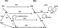
依据本发明的一个实施例,该总线协议被重调或者修改以把在连续阶段开始之间的等待时间或者延迟调整到更接近地匹配用于该处理器总线的、两个总线时钟周期的新拍频。图7是一个框图,说明了在事务阶段(包括判优、请求、探听和响应阶段)之间的最少等待时间延迟。显示了用于两个事务(事务1和事务2)的判优(Arb)、请求(Req)、探听和响应(Resp)阶段。显示的数字用来指示在阶段之间的一个等待时间或者延迟。第一个数字指示如在某些奔腾处理器中实现的那样,在阶段开始之间的总线时钟周期的最小数目,而第二个数字(其括号内)指示在该总线协议被调整或者重调以更接近地匹配两个总线时钟周期的新拍频之后,在阶段之间新的最小等待时间。如果仅仅显示了一个数字,则这指示在某些奔腾处理器和该发明的一个实施例之间,在阶段之间的延迟或者等待时间中没有变化。According to one embodiment of the invention, the bus protocol is retuned or modified to adjust the latency or delay between the start of successive phases to more closely match the new two bus clock cycles for the processor bus. beat frequency. Figure 7 is a block diagram illustrating the minimum latency delay between transaction phases including the arbitration, request, snoop and response phases. The Arbitration (Arb), Request (Req), Snoop and Response (Resp) phases for two transactions (
如上所述,在图7中显示的、在阶段之间的最小等待时间一般是两个总线时钟周期。参考图7,用于一个事务(例如,事务1)的、在一个判优阶段开始和一个请求阶段开始之间的最小等待时间在两个总线时钟周期处保持不变。从一个事务的请求阶段开始到一个事务的探听阶段开始的最小等待时间已经从四个总线时钟周期减少到三个周期。在一个探听阶段开始和一个响应阶段开始之间的最小等待时间在两个总线时钟周期处保持不变。在请求阶段开始和一个目标代理能够断定TRDY#信号时候之间的最小等待时间已经从三个总线时钟周期减少到两个总线时钟周期。从断定该TRDY#信号到一个响应阶段开始的最小等待时间在两个总线时钟周期处保持不变。As mentioned above, the minimum latency between phases shown in Figure 7 is typically two bus clock cycles. Referring to FIG. 7, the minimum latency between the start of an arbitration phase and the start of a request phase for a transaction (eg, transaction 1) remains constant at two bus clock cycles. The minimum latency from the start of the request phase of a transaction to the start of the snoop phase of a transaction has been reduced from four bus clock cycles to three. The minimum latency between the start of a snoop phase and the start of a response phase remains constant at two bus clock cycles. The minimum latency between the start of the request phase and when a target agent is able to assert the TRDY# signal has been reduced from three bus clock cycles to two bus clock cycles. The minimum latency from assertion of the TRDY# signal to the start of a response phase remains constant at two bus clock cycles.
此外,在连续事务的同一个或者相应阶段之间的最小等待时间已经被修改为更接近地匹配两个时钟周期的拍频。再次参考图7,在连续的判优阶段之间的最小等待时间(例如在事务1的判优阶段开始和事务2的判优阶段开始之间的最小等待时间)已经从三个总线时钟周期减少到两个周期。该在连续请求阶段之间的最小等待时间已经从三个总线时钟周期减少到两个。该在连续探听阶段之间的最小等待时间已经从三个总线时钟周期减少到两个。而且,该在连续响应阶段之间的最小等待时间已经从三个总线时钟周期减少到两个。Additionally, the minimum latency between the same or corresponding phases of consecutive transactions has been modified to more closely match the beat frequency of two clock cycles. Referring again to FIG. 7, the minimum latency between successive arbitration phases (e.g., the minimum latency between the start of the arbitration phase of
将结合对在阶段之间的等待时间下降有贡献的、对该总线协议的某些改变或者修改(在发生等待时间减少的地方)的一个简要说明,对每一个阶段进行描述。Each phase will be described in conjunction with a brief description of certain changes or modifications to the bus protocol (where latency reduction occurs) that contribute to latency reduction between phases.
当一个请求代理不拥有该总线时,事务从一个判优阶段开始,其中一个请求代理变为该总线所有者。在该请求代理变为该总线所有者之后,该事务进入该请求阶段。在该请求阶段的第一个子阶段(子阶段a),和该事务地址和足够的信息一起驱动一个ADS#信号(指示有效地址)以开始探听和存储器存取。在该请求阶段的第二个子阶段(子阶段b),用于该请求的各种辅助信息被驱动到总线117上,包括字节使能(指示哪个数据字节将在该数据线上提供)、一个延期ID、事务长度及其他事务信息。在一个总线时钟周期期间驱动第一个和第二个子阶段。结果,依据一个实施例,该请求信息(例如,它的大部分经由地址总线提供)据说具有一个2x数据传送率。When a requesting agent does not own the bus, the transaction begins with an arbitration phase in which a requesting agent becomes the owner of the bus. After the requesting agent becomes the bus owner, the transaction enters the request phase. In the first subphase of the request phase (subphase a), an ADS# signal (indicating a valid address) is driven with the transaction address and sufficient information to initiate snoops and memory accesses. In the second subphase of the request phase (subphase b), various ancillary information for the request is driven onto bus 117, including byte enables (indicating which data byte is to be presented on that data line) , a deferred ID, transaction length, and other transaction information. The first and second sub-stages are driven during one bus clock cycle. Consequently, the request message (eg, most of which is provided via the address bus) is said to have a 2x data transfer rate, according to one embodiment.
依据一个实施例,每个事务都具有一个探听阶段。由该探听阶段产生的探听指示为一个事务驱动的地址是否引用在任何总线代理的高速缓存中的一个正确或者修改了(脏)的高速缓存线。该探听结果还指示一个事务是否将按次序完成,或者可以为可能的元序完成延期。如果一个代理没有准备通过扩展该探听阶段来探听的话,该代理能够使用一个探听停止延迟一个事务。According to one embodiment, each transaction has a snoop phase. The snoops generated by the snoop phase indicate whether the address driven for a transaction references a valid or modified (dirty) cache line in any bus agent's cache. The snoop result also indicates whether a transaction will complete in-order, or can be deferred for possible out-of-order completion. An agent can use a snoop stop to delay a transaction if it is not prepared to snoop by extending the snoop phase.
现在将描述每一个阶段,并且突出该被实现以减少在阶段之间的等待时间的差别(在合适的地方)。Each phase will now be described, highlighting what is implemented to reduce the difference in latency between phases (where appropriate).
1)判优阶段:没有事务能够被发布直到该总线代理拥有该处理器总线117为止。如果想要驱动该事务到该处理器总线117上的代理还没有拥有该总线117,这一个事务仅仅需要具有这个阶段。依据一个实施例,提供了一个支持两种类型总线代理的总线判优协议,该总线代理为:对称代理、以及优先级代理。在总线117上的处理器一般作为对称代理进行判优。优先级代理(例如,系统接口116)通常以该I/O子系统(I/O桥124或者I/O代理)和存储器子系统(位于主存储器子系统122中的存储器代理)名义进行判优。1) Arbitration phase: no transaction can be issued until the bus agent owns the processor bus 117 . A transaction only needs to have this phase if the agent that wants to drive the transaction onto the processor bus 117 does not already own the bus 117. According to one embodiment, a bus arbitration protocol supporting two types of bus agents is provided: a symmetric agent and a priority agent. Processors on bus 117 typically arbitrate as symmetric proxies. A priority agent (e.g., system interface 116) typically arbitrates on behalf of the I/O subsystem (I/O bridge 124 or I/O agent) and the memory subsystem (the memory agent located in main memory subsystem 122) .
一个可用于为总线所有权判优的示例信号群显示如下(如在这里使用的那样,#符号指示有效低电平信号):An example signal group that can be used to arbitrate for bus ownership is shown below (as used here, the # symbol indicates an active low signal):
示例判优信号
处理器总线117允许多个代理同时为该总线117判优。该对称代理基于循环轮流优先权方案为总线117进行判优。该判优方案确保所有的对称代理公平地进入一个请求阶段。每个对称代理都具有一个唯一的、在重置处分配的代理ID(例如,代理0,1,2,3)而且将以循环次序发生判优。在重置之后,代理0具有最高的优先级,继之以代理1、2、和3。每个对称代理保持一个反映最近总线所有者的对称代理ID的公共轮流ID。在每个判优事件上,如果没有其他较高优先级的动作阻止该总线使用的话,该具有最高优先级的对称代理变为所有者并且可以进入该请求阶段。优先级代理比对称所有者具有更高的优先级。The processor bus 117 allows multiple agents to arbitrate for the bus 117 simultaneously. The symmetric proxy arbitrates for the bus 117 based on a round robin priority scheme. The arbitration scheme ensures that all symmetric agents enter a request phase fairly. Each symmetric proxy has a unique proxy ID assigned at reset (eg,
一个对称代理通过断定它的BREQn#信号来请求总线。基于在BREQ[3:0]上采样的值以及最后的对称总线所有者,所有代理能够同时确定下一个对称总线所有者。一个优先级代理通过断定BPRI#来要求该总线,其临时地覆盖该判优方案,因为没有别的对称代理将发布另一个解锁的总线事务直到BPRI#被采样为不活动为止。该优先级代理总是下一个总线的所有者。BNR#信号能够由任何总线代理断定以堵塞进一步的事务被发布到该总线上(通常当系统资源诸如缓存是满的而且不能容纳另一个事务时使用)。LOCK#信号的断定指示该总线代理正执行不可被中断的、一个基本的总线事务序列。A symmetric agent requests the bus by asserting its BREQn# signal. Based on the values sampled on BREQ[3:0] and the last symmetric bus owner, all agents can simultaneously determine the next symmetric bus owner. One priority agent claims the bus by asserting BPRI#, which temporarily overrides the arbitration scheme because no other symmetric agent will issue another unlocked bus transaction until BPRI# is sampled as inactive. The priority agent is always the next owner of the bus. The BNR# signal can be asserted by any bus agent to block further transactions from being issued on the bus (usually used when system resources such as buffers are full and cannot accommodate another transaction). The assertion of the LOCK# signal indicates that the bus agent is executing a basic sequence of bus transactions that cannot be interrupted.
该优先级代理能够在它产生它的最后请求的同一个周期中取消断定BPRI#并且释放总线所有权。在某些奔腾处理器中,在断定BPRI#信号之后,该BPRI#信号必须被取消断定至少两个总线时钟周期。这匹配老的3个总线时钟周期比率(在某些奔腾处理器中),所以提供了对称代理和优先级代理对该总线的平衡访问。依据一个实施例,该协议被改变为在BPRI#信号被断定之后需要该BPRI#信号被取消断定仅仅至少一个总线时钟周期。在一个当前实施例中的改变支持两个总线时钟周期拍率,一个总线时钟周期用于断定以及一个周期用于取消断定。The priority agent can deassert BPRI# and release bus ownership in the same cycle that it made its last request. In some Pentium processors, the BPRI# signal must be deasserted for at least two bus clock cycles after the BPRI# signal is asserted. This matches the old 3 bus clock cycle ratio (in some Pentium processors), so provides balanced access to the bus by both symmetric and prioritized agents. According to one embodiment, the protocol is changed to require the BPRI# signal to be deasserted only at least one bus clock cycle after the BPRI# signal is asserted. The change in one current embodiment supports a two bus clock cycle rate, one bus clock cycle for asserting and one cycle for deasserting.
应当注意:该BNR#信号可用于延迟进一步的请求,例如,当一个代理不具有足够的资源来支持另一个事务时。依据一个实施例,基于三个状态实现以及确定一个请求停止协议:It should be noted that this BNR# signal can be used to delay further requests, for example, when one agent does not have sufficient resources to support another transaction. According to one embodiment, a request to stop protocol is implemented and determined based on three states:
1)空闲:在这个状态中,一个代理发布请求的能力不由该BNR#请求停止协议限制,而是仅仅由该总线的所有权以及由该请求比率限制。在某些奔腾处理器中,在ADS#被采样断定之后三个时钟周期,发生在该空闲状态中的BNR#取样点。依据一个实施例,该BNR#取样点在该ADS#信号被采样断定之后被调整为发生两个时钟周期(而不是三个)。当一个代理在自由状态中试图停止一个新的请求产生时,该代理在从ADS#开始一个有效的BNR#采样点之前的时钟周期内驱动BNR#为有效。在下一个时钟周期内,所有的代理在一个BNR#采样点上监视一个活动的BNR#并且转换为停止状态。1) Idle: In this state, an agent's ability to issue requests is not limited by the BNR# request stop protocol, but only by ownership of the bus and by the request rate. In some Pentium processors, the BNR# sampling point in the idle state occurs three clock cycles after ADS# is sampled asserted. According to one embodiment, the BNR# sampling point is adjusted to occur two clock cycles (instead of three) after the ADS# signal is sampled asserted. When an agent in the free state attempts to stop a new request being generated, the agent drives BNR# active for the clock cycle before starting a valid BNR# sampling point from ADS#. During the next clock cycle, all agents monitor an active BNR# at a BNR# sampling point and transition to the STOP state.
2)调节:一旦一个代理具有该总线的所有权并且已经保持了最大的ADS#比率,一个代理可以在这个状态发布一个请求。该BNR#采样点是在该调节状态的第一个时钟周期。当在该调节状态中时,如果BNR#在一个BNR#采样点上被采样为有效,则该状态转移到停止状态。如果BNR#在一个BNR#采样点上被采样为无效,则该状态转移到空闲状态。2) Throttle: Once an agent has ownership of the bus and has maintained the maximum ADS# ratio, an agent can issue a request in this state. The BNR# sample point is the first clock cycle in the regulation state. While in the Regulate state, if BNR# is sampled active on one BNR# sampling point, the state transitions to the Stop state. If BNR# is sampled invalid at a BNR# sampling point, the state transitions to the Idle state.
3)停止:在这个状态中,一个代理可以不发布一个请求,直到在BNR#采样点采样的BNR#是无效为止。该BNR#采样点在当进入该停止状态时的总线时钟周期以及其它后续时钟周期中开始,只要BNR#在它的采样点处被采样为有效。在一个重置事件(要么INIT#要么RESET#)之后,一个请求停止状态总是被初始化为停止。一个代理能够通过每两个时钟周期断定BNR#(在有效采样点之前)来延伸该停止状态。如果BNR#在停止状态的同时没有被采样为有效,这该请求停止状态将转换到调节状态。3) Stop: In this state, an agent may not issue a request until the BNR# sampled at the BNR# sampling point is invalid. The BNR# sample point begins in the bus clock cycle when the STOP state is entered and other subsequent clock cycles as long as BNR# is sampled valid at its sample point. After a reset event (either INIT# or RESET#), a requested stop state is always initialized to stop. An agent can extend the stop state by asserting BNR# every two clock cycles (before the valid sample point). If BNR# is not sampled active while in the STOP state, the requested STOP state will transition to the Regulate state.
因此,要求该BPRI#信号被断定之后仅仅至少一个总线时钟周期(而不是两个)被取消断定,并且调整在该空闲状态中的BNR#采样点到发生在该ADS#信号被采样为断定之后两个时钟周期(而不是三个),可以把在连续判优阶段开始之间的最小等待时间从三个总线时钟周期减少到两个总线时钟周期。Therefore, it is required that the BPRI# signal be deasserted only at least one bus clock cycle (rather than two) after it is asserted, and that the BNR# sampling point in the idle state be adjusted to occur after the ADS# signal is sampled as asserted Two clock cycles (instead of three) reduces the minimum latency between the start of successive arbitration phases from three bus clock cycles to two bus clock cycles.
2)请求阶段:请求阶段是其中该事务实际上被发布或者驱动到总线上的阶段。依据一个实施例,该请求阶段是一个持续的公共总线时钟周期。该请求阶段包括两个子阶段,包括子阶段a(在该请求阶段的第一半期间)和子阶段b(在该请求阶段的第二子阶段期间)。包括事务地址的请求信息在该请求阶段期间传送。该请求阶段从断定该ADS#信号、地址选通脉冲信号开始。这里是可用于传送一个请求的示例信号组。2) Request phase: The request phase is the phase where the transaction is actually issued or driven onto the bus. According to one embodiment, the request phase is one continuous common bus clock cycle. The request phase comprises two sub-phases, including sub-phase a (during the first half of the request phase) and sub-phase b (during the second sub-phase of the request phase). Request information including the transaction address is transmitted during the request phase. The request phase begins by asserting the ADS# signal, address strobe signal. Here is an example set of signals that can be used to communicate a request.
示例请求信号
注意:Notice:
a.这些信号在该请求阶段的第一个子阶段(子阶段a)期间在该指示的引脚上驱动。a. These signals are driven on the indicated pins during the first subphase (subphase a) of the request phase.
b.这些信号在该请求阶段的第二个子阶段(于阶段b)期间被驱动。b. These signals are driven during the second subphase (in phase b) of the request phase.
因此,该事务地址在Aa[35:3](其中“A”指示地址线或者地址总线204而且“a”指示在子阶段a期间传送指示信号)上传送,而描述该事务的附加信息(例如,字节使能、属性、扩充功能)在Ab[35:3](“b”指示附加信息在于阶段b期间经由地址线传送)上传送。ADS#的断定定义了请求阶段的开始。更可取地是ADSTB[1:0]#应当在ADS#被断定的每个总线时钟周期中被触发一次,而不是在任何其他周期中。该REQa[4:0]#和REQb[4:0]#标识该事务类型。Thus, the transaction address is transmitted on Aa[35:3] (where "A" indicates an address line or address bus 204 and "a" indicates that an indication signal was transmitted during subphase a), while additional information describing the transaction (e.g. , Byte Enables, Attributes, Extended Functions) are transmitted on Ab[35:3] ("b" indicating that additional information was transmitted via address lines during phase b). The assertion of ADS# defines the beginning of the request phase. Preferably ADSTB[1:0]# should be toggled once in every bus clock cycle that ADS# is asserted, and not in any other cycle. The REQa[4:0]# and REQb[4:0]# identify the transaction type.
依据一个实施例,该请求能够被驱动到该处理器总线上:According to one embodiment, the request can be driven onto the processor bus:
1)在所有权观测之后的时钟周期;以及1) clock cycles after ownership observation; and
2)在为前一个事务断定ADS#之后的两个或更多时钟周期,以及2) Two or more clock cycles after ADS# was asserted for the previous transaction, and
3)BNR#被观察为无效时,以及3) When BNR# is observed to be invalid, and
4)如果不由这个代理激活的LOCK#,被观察为无效。4) If the LOCK# is not activated by this agent, it is observed to be invalid.
某些奔腾处理器在断定前一个事务的ADS#之后,在该请求能够被驱动到该处理器总线上之前,要求三个时钟周期的最小延迟。为了把在连续事务请求阶段之间的最小等待时间从三个时钟周期减少到两个时钟周期,依据一个实施例,一个代理可以在断定前一个事务的ADS#信号之后仅仅两个总线时钟周期之后把该请求驱动到该总线上。如上所述,该ADS#信号标识该请求阶段的开始,并且指示该请求的子阶段a正被驱动到该处理器总线上,该子阶段a包括一个地址(经由地址总线提供)和该请求(经由该REQ#[4:0线提供)。Certain Pentium processors require a minimum delay of three clock cycles after asserting the ADS# of a previous transaction before the request can be driven onto the processor bus. To reduce the minimum latency between successive transaction request phases from three clock cycles to two clock cycles, according to one embodiment, an agent can assert the ADS# signal of a previous transaction only two bus clock cycles after Drive the request onto the bus. As noted above, the ADS# signal identifies the beginning of the request phase and indicates that subphase a of the request is being driven onto the processor bus, the subphase a including an address (provided via the address bus) and the request ( provided via the REQ#[4:0 line).
3)探听阶段:依据一个实施例,该处理器总线支持用于多个高速缓存代理的高速缓存一致性。一致性(或者数据一致性)确保具有多级高速缓存和存储器和多个高速缓存代理的一个系统或者计算机给出一个共享存储器模型,其中更可取地是没有代理曾经该取旧的(或者错误的)数据并且按要求动作能够被串行化。一条线是在该高速缓存代理中的高速缓存单元。依据一个实施例,一条高速缓存线是64个字节,但是能够使用其他尺寸的高速缓存线。3) Snoop phase: According to one embodiment, the processor bus supports cache coherency for multiple caching agents. Consistency (or data consistency) ensures that a system or computer with multiple levels of cache and memory and multiple caching agents gives a shared memory model where preferably no agent should ever fetch old (or wrong) ) data and actions can be serialized on demand. A line is a cache unit in the caching proxy. According to one embodiment, a cache line is 64 bytes, but cache lines of other sizes can be used.
该高速缓存协议把线与状态相关联并且定义控制状态转换的规则。每条线在每个高速缓存中都具有一个状态。依据一个实施例,存在有四个线状态,包括:M(修改),其指示该线在这个高速缓存中并且包含该线一个比在存储器中的更新的值,而且该线在所有其他代理中是无效的;E(排它)指示该线是在这个高速缓存中并且与在存储器中的值相同,并且在所有其他代理中是无效的;S(共享)指示该线是在这个高速缓存中,包含和在存储器中的相同的值,并且可以在其他代理中;而且I(元效)指示该线在这个高速缓存中不是可用的并且应当从另一个高速缓存或者代理处取出。The cache protocol associates lines with states and defines rules governing state transitions. Each line has a state in each cache. According to one embodiment, there are four line states, including: M (Modified), which indicates that the line is in this cache and contains a newer value for the line than in memory, and that the line is in all other agents is invalid; E (exclusive) indicates that the line is in this cache with the same value as in memory, and is invalid in all other agents; S (shared) indicates that the line is in this cache , contains the same value as in memory, and may be in other agents; and I (ineffective) indicates that the line is not available in this cache and should be fetched from another cache or agent.
探听阶段是其中执行高速缓存一致性的阶段。以下是能够在一个探听阶段期间使用的探听信号示例列表:The snoop phase is the phase in which cache coherency is performed. The following is a list of sample snoop signals that can be used during a snoop phase:
示例探听信号
在该探听阶段,所有高速缓存代理驱动它们的探听结果并且参与到高速缓存一致性解决中。该代理为几乎所有的存储器事务,这就是说不是它拥有的,产生内部探听结果。所有高速缓存代理(探听代理)在这个阶段使用HIT#和HITM#信号驱动它们的探听结果到该总线上。在该探听阶段期间断定HIT#,以指示包含请求的数据的一条高速缓存线的一个拷贝驻留在另一个代理在这个接口上的高速缓存中。在该探听阶段期间断定HITM#,以指示包含请求的数据的一条高速缓存线的一个修改拷贝驻留在另一个代理在这个接口上的高速缓存中。如果HIT#和HITM#在一个探听阶段期间由一个代理同时断定,则已经发生了一个探听停止并且当前探听阶段应当被延伸。在该探听阶段期间断定DEFER#,以指示当前事务不保证能够完成。During this snoop phase, all caching proxies drive their snoop results and participate in cache coherency resolution. The agent generates internal snoop results for almost all memory transactions, that is to say not owned by it. All caching agents (snooping agents) drive their snoop results onto this bus at this stage using the HIT# and HITM# signals. A HIT# is asserted during the snoop phase to indicate that a copy of a cache line containing the requested data resides in another agent's cache on this interface. HITM# is asserted during the snoop phase to indicate that a modified copy of a cache line containing the requested data resides in another agent's cache on this interface. If HIT# and HITM# are asserted simultaneously by an agent during a snoop phase, a snoop stop has occurred and the current snoop phase should be extended. DEFER# is asserted during this snoop phase to indicate that the current transaction is not guaranteed to complete.
在某些奔腾处理器中,探听结果在ADS#信号被断定之后四个时钟周期被驱动,并且从前一个事务的探听阶段开始至少三个时钟周期。然而,依据一种实施例,这些最少等待时间被修改了以更接近地匹配该处理器总线的新拍频。依据一个实施例,该探听结果现在可以在ADS#信号被断定之后三个时钟周期(即在该请求阶段开始之后三个总线时钟周期)驱动并且在前一个事务的探听阶段之后至少两个时钟周期(即在用于前一个事务的探听结果被驱动到该总线上之后至少两个时钟周期)驱动。因此,用于HIT#/HITM#/DEFER#信号(探听结果)的最大激活比率从每三个总线时钟周期一次变为每两个总线时钟周期一次。注意由于该请求阶段被缩短了一个周期,从该请求阶段(子阶段B)结尾到该探听阶段的等待时间保持同样。In some Pentium processors, the snoop result is driven four clock cycles after the ADS# signal is asserted, and at least three clock cycles from the snoop phase of the previous transaction. However, according to one embodiment, these minimum latencies are modified to more closely match the new beat frequency of the processor bus. According to one embodiment, the snoop result may now be driven three clock cycles after the ADS# signal is asserted (i.e., three bus clock cycles after the start of the request phase) and at least two clock cycles after the previous transaction's snoop phase (ie, at least two clock cycles after the snoop result for the previous transaction was driven onto the bus). Therefore, the maximum activation rate for the HIT#/HITM#/DEFER# signal (snoop result) changes from once every three bus clock cycles to once every two bus clock cycles. Note that since the request phase is shortened by one cycle, the latency from the end of the request phase (subphase B) to the snoop phase remains the same.
4)响应阶段:在这个阶段,该响应代理驱动该事务响应到处理器总线上。在该请求阶段启动的请求进入一个由每个总线代理保持的排序队列。响应代理是负责完成在该排序队列顶端的事务的代理。该响应代理是由该事务在请求阶段期间寻址的设备或者代理。以下是能够在该响应阶段使用的一个示例信号组:4) Response phase: In this phase, the response agent drives the transaction response onto the processor bus. Requests initiated during the request phase enter an ordered queue maintained by each bus agent. The Response Broker is the broker responsible for completing transactions at the top of the queue. The responding proxy is the device or proxy addressed by the transaction during the request phase. Here is an example signal group that can be used in this response phase:
示例响应信号
该事务响应在该RS[2:0]#信号上被编码。可能的响应示例包括:一个标准数据响应(其中该响应代理被要求与该响应一起传输读取的数据)、一个重试响应(当在探听阶段期间断定DEFER#时指示该事务必须被重试)、一个延迟响应(其中该响应代理或者回应代理承诺将来使用该推迟答复事务完成该事务)、一个没有数据响应(其中没有数据将由该寻址的代理返回),等。TRDY#由该响应代理断定以指示它准备接受写入或者写回数据,等。该RSP信号提供用于该RS信号的奇偶校验。The transaction response is encoded on the RS[2:0]# signal. Examples of possible responses include: a standard data response (where the responding proxy is asked to transmit read data along with the response), a retry response (indicating that the transaction must be retried when DEFER# is asserted during the snoop phase) , a delayed response (wherein the responding proxy or the responding proxy commits to using the deferred reply transaction to complete the transaction in the future), a no data response (where no data will be returned by the addressed proxy), etc. TRDY# is asserted by the responding agent to indicate that it is ready to accept writes or write back data, etc. The RSP signal provides parity for the RS signal.
在某些奔腾处理器中,该响应能够在前一个事务的响应阶段之后最少三个总线时钟周期之后被驱动。依据一个实施例,这个在连续事务的响应阶段之间的最小等待时间被调整为更接近地匹配该处理器总线的新拍频。依据一个实施例,该响应能够在前一个事务的响应之后最少两个总线时钟周期之后被驱动。这个最小等待时间一般受可以延伸这个等待时间的其他限制影响。由于该双重抽吸信号模式用于该请求信号,每两个总线时钟周期就能够驱动一个响应一次(相比之下,某些奔腾处理器每三个总线时钟周期一次)。In some Pentium processors, the response can be driven a minimum of three bus clock cycles after the response phase of the previous transaction. According to one embodiment, the minimum latency between response phases of successive transactions is adjusted to more closely match the new beat frequency of the processor bus. According to one embodiment, the response can be driven a minimum of two bus clock cycles after the previous transaction's response. This minimum wait time is generally affected by other constraints that may extend this wait time. Since the double-pump signaling mode is used for the request signal, a response can be driven once every two bus clock cycles (compared to every three bus clock cycles for some Pentium processors).
一个请求启动事务是一个其中该请求代理已经写入要传输的数据的事务。该被寻址的代理断定TRDY#以指示它从该打算执行一个写操作的请求代理接收数据的能力。在某些奔腾处理器中,该TRDY#信号能够在用于同一个事务的ADS#信号被断定之后最少三个总线时钟周期之后被断定。一般地其他能够延长这个等待时间的限制。这个等待时间被修改为更接近地匹配该处理器总线新的拍频。依据一个实施例,一个被寻址的代理能够在用于同一个事务的ADS#信号被断定之后最少两个总线时钟周期之后断定该TRDY#信号。注意从该请求阶段结尾到TRDY#的等待时间保持不变。A request-initiated transaction is one in which the requesting agent has written data to be transferred. The addressed agent asserts TRDY# to indicate its ability to receive data from the requesting agent intending to perform a write operation. In some Pentium processors, the TRDY# signal can be asserted a minimum of three bus clock cycles after the ADS# signal is asserted for the same transaction. Typically other constraints can extend this waiting time. This latency is modified to more closely match the new beat frequency of the processor bus. According to one embodiment, an addressed agent can assert the TRDY# signal a minimum of two bus clock cycles after the ADS# signal was asserted for the same transaction. Note that the wait time from the end of the request phase to TRDY# remains constant.
5)数据(传输)阶段:在该数据阶段期间,数据经由处理器总线117在不同的总线代理之间传输。基于该请求阶段,一个事务包含一个“请求启动”(写)数据传送、一个“响应启动”(读)数据传送、或者没有数据传送。该数据阶段可以与用于一个事务的请求阶段相一致。5) Data (transfer) phase: During this data phase, data is transferred between different bus agents via the processor bus 117 . Based on the request phase, a transaction contains a "request-initiated" (write) data transfer, a "response-initiated" (read) data transfer, or no data transfer. The data phase may coincide with the request phase for a transaction.
以下是能够在该数据阶段中使用的一个信号示例列表:Here is an example list of signals that can be used in this data phase:
示例数据信号
DRDY#指示有效数据已经放置在总线117上并且必须被锁存。该数据总线所有者为每个总线时钟周期断定DRDY#,在该总线时钟周期中将要传输有效数据。DRDY#能够被取消断定为在该数据阶段中插入等待状态。DBSY#可用于在第一个DRDY#断定之前并且在连续的DRDY#断定之间,为一个多重总线时钟数据传送保持该数据总线DINV[3:]#用来指示该数据位已经由该数据源反转了。DRDY# indicates that valid data has been placed on bus 117 and must be latched. The data bus owner asserts DRDY# for each bus clock cycle in which valid data is to be transferred. DRDY# can be deasserted to insert a wait state in the data phase. DBSY# can be used to hold the data bus for a multiple bus clock data transfer before the first DRDY# assertion and between successive DRDY# assertions. reversed.
数据总线206(图2)的数据信号D[63:0]#提供了在总线代理之间的一个64位数据通路。为了一个部分传输,包括I/O读取和I/O写事务,该字节使能信号(BE[7:0]#)确定该数据总线的哪个字节将包含该有效数据。该DP信号可被用于为该数据信号提供奇偶校验。Data signal D[63:0]# of data bus 206 (FIG. 2) provides a 64-bit data path between bus agents. For a partial transfer, including I/O read and I/O write transactions, the byte enable signal (BE[7:0]#) determines which byte of the data bus will contain the valid data. The DP signal can be used to provide parity for the data signal.
依据一个实施例,数据可以使用一个四重抽吸(即,4X)源同步锁存协议来传输,其中该数据信号D[63:0]被用来在单个总线时钟周期内传送四个8字节数据单元。第一个8字节(以爆发次序)由该总线时钟的第一个四分之一传送,在总线时钟的第二个四分之一中传送第二个8字节单元,在该总线时钟的第三个四分之一中传送该第三个8字节单元以及在该总线时钟的第四个四分之一中传送第四个8字节单元。如果要被传输的数据是1到8字节长,则该数据能够在该总线时钟的第一个四分之一中传输,而且如果该数据是9-16字节长,则该数据能够在该总线时钟的头两个四分之一中传输。According to one embodiment, data may be transferred using a quadruple pumped (i.e., 4X) source synchronous latch protocol, where the data signals D[63:0] are used to transfer four 8-word section data unit. The first 8-byte (in burst order) is transferred by the first quarter of the bus clock, the second 8-byte unit is transferred in the second quarter of the bus clock, and the The third octet is transmitted in the third quarter of the bus clock and the fourth octet is transmitted in the fourth quarter of the bus clock. If the data to be transferred is 1 to 8 bytes long, the data can be transferred in the first quarter of the bus clock, and if the data is 9-16 bytes long, the data can be transferred in the The bus clock is transmitted during the first two quarters.
在这里具体说明和/或描述了本发明的几个实施例。然而,应当理解:本发明的修改和变化由上述示教所覆盖并且在附加权利要求的范围之内,而不背离本发明的精神上和想要的范围。Several embodiments of the invention are illustrated and/or described herein. It is to be understood, however, that modifications and variations of the present invention are covered by the above teachings and are within the purview of the appended claims without departing from the spirit and intended scope of the invention.
Claims (23)
Translated fromChineseApplications Claiming Priority (3)
| Application Number | Priority Date | Filing Date | Title |
|---|---|---|---|
| US09/474,058US6609171B1 (en) | 1999-12-29 | 1999-12-29 | Quad pumped bus architecture and protocol |
| US09/474,058 | 1999-12-29 | ||
| US09/474058 | 1999-12-29 |
Related Parent Applications (1)
| Application Number | Title | Priority Date | Filing Date |
|---|---|---|---|
| CNB008179840ADivisionCN1230762C (en) | 1999-12-29 | 2000-12-29 | Method and device for transmitting information on multipoint bidirectional bus |
Related Child Applications (1)
| Application Number | Title | Priority Date | Filing Date |
|---|---|---|---|
| CN2006100996516ADivisionCN1900924B (en) | 1999-12-29 | 2000-12-29 | Quad pumped bus architecture and protocol |
Publications (2)
| Publication Number | Publication Date |
|---|---|
| CN1815463Atrue CN1815463A (en) | 2006-08-09 |
| CN1815463B CN1815463B (en) | 2014-03-05 |
Family
ID=23882019
Family Applications (4)
| Application Number | Title | Priority Date | Filing Date |
|---|---|---|---|
| CN2006100996516AExpired - Fee RelatedCN1900924B (en) | 1999-12-29 | 2000-12-29 | Quad pumped bus architecture and protocol |
| CNB008179840AExpired - Fee RelatedCN1230762C (en) | 1999-12-29 | 2000-12-29 | Method and device for transmitting information on multipoint bidirectional bus |
| CNB200410061753XAExpired - Fee RelatedCN100375075C (en) | 1999-12-29 | 2000-12-29 | Quad pumped bus architecture and protocol |
| CN200410061754.4AExpired - Fee RelatedCN1815463B (en) | 1999-12-29 | 2000-12-29 | Quad pumping bus architecture and protocol |
Family Applications Before (3)
| Application Number | Title | Priority Date | Filing Date |
|---|---|---|---|
| CN2006100996516AExpired - Fee RelatedCN1900924B (en) | 1999-12-29 | 2000-12-29 | Quad pumped bus architecture and protocol |
| CNB008179840AExpired - Fee RelatedCN1230762C (en) | 1999-12-29 | 2000-12-29 | Method and device for transmitting information on multipoint bidirectional bus |
| CNB200410061753XAExpired - Fee RelatedCN100375075C (en) | 1999-12-29 | 2000-12-29 | Quad pumped bus architecture and protocol |
Country Status (16)
| Country | Link |
|---|---|
| US (6) | US6609171B1 (en) |
| EP (2) | EP1881414A3 (en) |
| JP (1) | JP4194274B2 (en) |
| KR (1) | KR100565101B1 (en) |
| CN (4) | CN1900924B (en) |
| AT (1) | ATE377797T1 (en) |
| AU (1) | AU2463101A (en) |
| BR (1) | BRPI0016834B1 (en) |
| DE (2) | DE10085385B3 (en) |
| GB (1) | GB2374264B (en) |
| HK (1) | HK1046964B (en) |
| RU (1) | RU2271566C2 (en) |
| SG (2) | SG123610A1 (en) |
| TW (1) | TW559704B (en) |
| WO (1) | WO2001048621A1 (en) |
| ZA (1) | ZA200203946B (en) |
Families Citing this family (106)
| Publication number | Priority date | Publication date | Assignee | Title |
|---|---|---|---|---|
| US6609171B1 (en)* | 1999-12-29 | 2003-08-19 | Intel Corporation | Quad pumped bus architecture and protocol |
| US6965648B1 (en)* | 2000-05-04 | 2005-11-15 | Sun Microsystems, Inc. | Source synchronous link integrity validation |
| US6745268B1 (en)* | 2000-08-11 | 2004-06-01 | Micron Technology, Lnc. | Capacitive multidrop bus compensation |
| US6816932B2 (en)* | 2000-10-06 | 2004-11-09 | Broadcom Corporation | Bus precharge during a phase of a clock signal to eliminate idle clock cycle |
| US6678767B1 (en)* | 2000-10-06 | 2004-01-13 | Broadcom Corp | Bus sampling on one edge of a clock signal and driving on another edge |
| US6901475B2 (en)* | 2000-12-07 | 2005-05-31 | Micron Technology, Inc. | Link bus for a hub based computer architecture |
| US6993612B2 (en)* | 2000-12-07 | 2006-01-31 | Micron Technology, Inc. | Arbitration method for a source strobed bus |
| US7676588B2 (en)* | 2001-10-05 | 2010-03-09 | International Business Machines Corporation | Programmable network protocol handler architecture |
| DE50113128D1 (en) | 2001-12-03 | 2007-11-22 | Infineon Technologies Ag | Data communications equipment |
| US7000065B2 (en)* | 2002-01-02 | 2006-02-14 | Intel Corporation | Method and apparatus for reducing power consumption in a memory bus interface by selectively disabling and enabling sense amplifiers |
| US6983348B2 (en)* | 2002-01-24 | 2006-01-03 | Intel Corporation | Methods and apparatus for cache intervention |
| US7085889B2 (en)* | 2002-03-22 | 2006-08-01 | Intel Corporation | Use of a context identifier in a cache memory |
| CN100354843C (en)* | 2002-05-24 | 2007-12-12 | 皇家飞利浦电子股份有限公司 | Pseudo-multiport data memory with quiesce |
| EP1508108A4 (en)* | 2002-05-28 | 2008-11-05 | Cadence Design Systems Inc | Assertion-based transaction recording |
| TWI282513B (en)* | 2002-06-12 | 2007-06-11 | Mediatek Inc | A pre-fetch device of instruction for an embedded system |
| TW579467B (en)* | 2002-07-24 | 2004-03-11 | Via Tech Inc | Method for blocking request to bus |
| US7234034B2 (en)* | 2002-09-16 | 2007-06-19 | Texas Instruments Incorporated | Self-clocking memory device |
| US6956789B2 (en)* | 2002-09-16 | 2005-10-18 | Texas Instruments Incorporated | Cycle ready circuit for self-clocking memory device |
| US7200730B2 (en)* | 2002-09-16 | 2007-04-03 | Texas Instruments Incorporated | Method of operating a memory at high speed using a cycle ready status output signal |
| US8185602B2 (en) | 2002-11-05 | 2012-05-22 | Newisys, Inc. | Transaction processing using multiple protocol engines in systems having multiple multi-processor clusters |
| US7051229B2 (en)* | 2002-12-03 | 2006-05-23 | Alcatel Canada Inc. | Logical bus overlay for increasing the existing system bus data rate |
| US7216240B2 (en)* | 2002-12-11 | 2007-05-08 | Intel Corporation | Apparatus and method for address bus power control |
| US20040128416A1 (en)* | 2002-12-11 | 2004-07-01 | Tsvika Kurts | Apparatus and method for address bus power control |
| US7152167B2 (en)* | 2002-12-11 | 2006-12-19 | Intel Corporation | Apparatus and method for data bus power control |
| US20040117708A1 (en)* | 2002-12-16 | 2004-06-17 | Ellis David G. | Pre-announce signaling for interconnect built-in self test |
| US6922769B2 (en)* | 2002-12-23 | 2005-07-26 | Intel Corporation | Apparatus and method for reduction of power consumption in OS that use flat segmentation memory model |
| US20040153611A1 (en)* | 2003-02-04 | 2004-08-05 | Sujat Jamil | Methods and apparatus for detecting an address conflict |
| US7054988B2 (en)* | 2003-04-17 | 2006-05-30 | Lsi Logic Corporation | Bus interface for processor |
| US7478025B1 (en)* | 2003-04-18 | 2009-01-13 | Unisys Corporation | System and method to support dynamic partitioning of units to a shared resource |
| US20040230188A1 (en)* | 2003-05-12 | 2004-11-18 | Iulian Cioanta | Treatment catheters with thermally insulated regions |
| US7287126B2 (en)* | 2003-07-30 | 2007-10-23 | Intel Corporation | Methods and apparatus for maintaining cache coherency |
| US9087036B1 (en) | 2004-08-12 | 2015-07-21 | Sonics, Inc. | Methods and apparatuses for time annotated transaction level modeling |
| US8504992B2 (en)* | 2003-10-31 | 2013-08-06 | Sonics, Inc. | Method and apparatus for establishing a quality of service model |
| US7665069B2 (en)* | 2003-10-31 | 2010-02-16 | Sonics, Inc. | Method and apparatus for establishing a quality of service model |
| US7113000B2 (en)* | 2003-12-10 | 2006-09-26 | Hewlett-Packard Development Company, L.P. | Bus agent having multiple reference levels |
| US7178048B2 (en)* | 2003-12-23 | 2007-02-13 | Hewlett-Packard Development Company, L.P. | System and method for signal synchronization based on plural clock signals |
| US7057414B2 (en)* | 2004-01-07 | 2006-06-06 | International Business Machines Corporation | Avoiding oscillation in self-synchronous bi-directional communication system |
| US20050262376A1 (en)* | 2004-05-21 | 2005-11-24 | Mcbain Richard A | Method and apparatus for bussed communications |
| US7389375B2 (en) | 2004-07-30 | 2008-06-17 | International Business Machines Corporation | System, method and storage medium for a multi-mode memory buffer device |
| US7224595B2 (en)* | 2004-07-30 | 2007-05-29 | International Business Machines Corporation | 276-Pin buffered memory module with enhanced fault tolerance |
| US20060036826A1 (en)* | 2004-07-30 | 2006-02-16 | International Business Machines Corporation | System, method and storage medium for providing a bus speed multiplier |
| US7539800B2 (en)* | 2004-07-30 | 2009-05-26 | International Business Machines Corporation | System, method and storage medium for providing segment level sparing |
| US7296129B2 (en)* | 2004-07-30 | 2007-11-13 | International Business Machines Corporation | System, method and storage medium for providing a serialized memory interface with a bus repeater |
| US20060075164A1 (en)* | 2004-09-22 | 2006-04-06 | Ooi Eng H | Method and apparatus for using advanced host controller interface to transfer data |
| US7299313B2 (en)* | 2004-10-29 | 2007-11-20 | International Business Machines Corporation | System, method and storage medium for a memory subsystem command interface |
| US7395476B2 (en)* | 2004-10-29 | 2008-07-01 | International Business Machines Corporation | System, method and storage medium for providing a high speed test interface to a memory subsystem |
| US7277988B2 (en)* | 2004-10-29 | 2007-10-02 | International Business Machines Corporation | System, method and storage medium for providing data caching and data compression in a memory subsystem |
| US7441060B2 (en)* | 2004-10-29 | 2008-10-21 | International Business Machines Corporation | System, method and storage medium for providing a service interface to a memory system |
| US7331010B2 (en) | 2004-10-29 | 2008-02-12 | International Business Machines Corporation | System, method and storage medium for providing fault detection and correction in a memory subsystem |
| US7512762B2 (en) | 2004-10-29 | 2009-03-31 | International Business Machines Corporation | System, method and storage medium for a memory subsystem with positional read data latency |
| US7305574B2 (en)* | 2004-10-29 | 2007-12-04 | International Business Machines Corporation | System, method and storage medium for bus calibration in a memory subsystem |
| US7356737B2 (en)* | 2004-10-29 | 2008-04-08 | International Business Machines Corporation | System, method and storage medium for testing a memory module |
| TWI268427B (en)* | 2004-11-02 | 2006-12-11 | Via Tech Inc | Coordinating method of bus data transmission specification |
| TWI256558B (en)* | 2004-11-02 | 2006-06-11 | Via Tech Inc | Method for coordinating bus data transmission specification and CPU and bridge chip used in the same |
| TWI304935B (en)* | 2004-11-02 | 2009-01-01 | Via Tech Inc | Method for determining data transmission specification and combination of bridge chipset and memory used in the same |
| US20060171233A1 (en)* | 2005-01-18 | 2006-08-03 | Khaled Fekih-Romdhane | Near pad ordering logic |
| US20060161743A1 (en)* | 2005-01-18 | 2006-07-20 | Khaled Fekih-Romdhane | Intelligent memory array switching logic |
| KR100606244B1 (en)* | 2005-02-11 | 2006-07-28 | 삼성전자주식회사 | Method of capturing data transmitted in synchronization with data strobe signal and data capture circuit therefor |
| US7340568B2 (en)* | 2005-02-11 | 2008-03-04 | International Business Machines Corporation | Reducing number of rejected snoop requests by extending time to respond to snoop request |
| US7529955B2 (en) | 2005-06-30 | 2009-05-05 | Intel Corporation | Dynamic bus parking |
| US7543094B2 (en)* | 2005-07-05 | 2009-06-02 | Via Technologies, Inc. | Target readiness protocol for contiguous write |
| US7457901B2 (en)* | 2005-07-05 | 2008-11-25 | Via Technologies, Inc. | Microprocessor apparatus and method for enabling variable width data transfers |
| CN100461142C (en)* | 2005-07-05 | 2009-02-11 | 威盛电子股份有限公司 | Microprocessor, processor bus system, and method for performing sparse write processing |
| CN100527115C (en)* | 2005-07-11 | 2009-08-12 | 威盛电子股份有限公司 | Flexible width data protocol |
| CN100468382C (en)* | 2005-07-11 | 2009-03-11 | 威盛电子股份有限公司 | System and method for quadruple frequency address bus |
| US7502880B2 (en)* | 2005-07-11 | 2009-03-10 | Via Technologies, Inc. | Apparatus and method for quad-pumped address bus |
| US7441064B2 (en)* | 2005-07-11 | 2008-10-21 | Via Technologies, Inc. | Flexible width data protocol |
| US7444472B2 (en)* | 2005-07-19 | 2008-10-28 | Via Technologies, Inc. | Apparatus and method for writing a sparsely populated cache line to memory |
| US7590787B2 (en)* | 2005-07-19 | 2009-09-15 | Via Technologies, Inc. | Apparatus and method for ordering transaction beats in a data transfer |
| CN100435123C (en)* | 2005-07-19 | 2008-11-19 | 威盛电子股份有限公司 | Apparatus and method for sparse line write operations |
| US7444448B2 (en)* | 2005-08-03 | 2008-10-28 | Via Technologies, Inc. | Data bus mechanism for dynamic source synchronized sampling adjust |
| US20070073977A1 (en)* | 2005-09-29 | 2007-03-29 | Safranek Robert J | Early global observation point for a uniprocessor system |
| US7634609B2 (en)* | 2005-09-29 | 2009-12-15 | Via Technologies, Inc. | Data transmission coordinating method |
| US7757031B2 (en)* | 2005-10-24 | 2010-07-13 | Via Technologies, Inc. | Data transmission coordinating method and system |
| US7478259B2 (en)* | 2005-10-31 | 2009-01-13 | International Business Machines Corporation | System, method and storage medium for deriving clocks in a memory system |
| US7685392B2 (en)* | 2005-11-28 | 2010-03-23 | International Business Machines Corporation | Providing indeterminate read data latency in a memory system |
| US7636813B2 (en)* | 2006-05-22 | 2009-12-22 | International Business Machines Corporation | Systems and methods for providing remote pre-fetch buffers |
| US7594055B2 (en)* | 2006-05-24 | 2009-09-22 | International Business Machines Corporation | Systems and methods for providing distributed technology independent memory controllers |
| US7584336B2 (en)* | 2006-06-08 | 2009-09-01 | International Business Machines Corporation | Systems and methods for providing data modification operations in memory subsystems |
| US7493439B2 (en) | 2006-08-01 | 2009-02-17 | International Business Machines Corporation | Systems and methods for providing performance monitoring in a memory system |
| US7669086B2 (en) | 2006-08-02 | 2010-02-23 | International Business Machines Corporation | Systems and methods for providing collision detection in a memory system |
| US7581073B2 (en)* | 2006-08-09 | 2009-08-25 | International Business Machines Corporation | Systems and methods for providing distributed autonomous power management in a memory system |
| US7587559B2 (en) | 2006-08-10 | 2009-09-08 | International Business Machines Corporation | Systems and methods for memory module power management |
| US7539842B2 (en) | 2006-08-15 | 2009-05-26 | International Business Machines Corporation | Computer memory system for selecting memory buses according to physical memory organization information stored in virtual address translation tables |
| US7490217B2 (en) | 2006-08-15 | 2009-02-10 | International Business Machines Corporation | Design structure for selecting memory busses according to physical memory organization information stored in virtual address translation tables |
| US20080062892A1 (en)* | 2006-09-07 | 2008-03-13 | Honeywell International Inc. | High speed bus protocol with programmable scheduler |
| US7477522B2 (en)* | 2006-10-23 | 2009-01-13 | International Business Machines Corporation | High density high reliability memory module with a fault tolerant address and command bus |
| US7870459B2 (en)* | 2006-10-23 | 2011-01-11 | International Business Machines Corporation | High density high reliability memory module with power gating and a fault tolerant address and command bus |
| US8868397B2 (en)* | 2006-11-20 | 2014-10-21 | Sonics, Inc. | Transaction co-validation across abstraction layers |
| KR100903381B1 (en)* | 2006-11-24 | 2009-06-23 | 주식회사 하이닉스반도체 | Semiconductor memory device and driving method thereof |
| KR20080047027A (en)* | 2006-11-24 | 2008-05-28 | 주식회사 하이닉스반도체 | Semiconductor memory device and driving method thereof |
| KR100915811B1 (en)* | 2006-12-07 | 2009-09-07 | 주식회사 하이닉스반도체 | Data Input / Output Control Signal Generation Circuit of Semiconductor Memory Device |
| US7721140B2 (en) | 2007-01-02 | 2010-05-18 | International Business Machines Corporation | Systems and methods for improving serviceability of a memory system |
| US7603526B2 (en)* | 2007-01-29 | 2009-10-13 | International Business Machines Corporation | Systems and methods for providing dynamic memory pre-fetch |
| US7606988B2 (en) | 2007-01-29 | 2009-10-20 | International Business Machines Corporation | Systems and methods for providing a dynamic memory bank page policy |
| US20090132747A1 (en)* | 2007-11-19 | 2009-05-21 | International Business Machines Corporation | Structure for universal peripheral processor system for soc environments on an integrated circuit |
| US8139697B2 (en)* | 2008-01-29 | 2012-03-20 | United Microelectronics Corp. | Sampling method and data recovery circuit using the same |
| US8020167B2 (en)* | 2008-05-05 | 2011-09-13 | Dell Products L.P. | System and method for automatic throttling of resources in an information handling system chassis |
| KR101642833B1 (en)* | 2010-02-05 | 2016-07-26 | 삼성전자주식회사 | clock embedded interface method, transceiver and display device using the method |
| WO2012127599A1 (en)* | 2011-03-22 | 2012-09-27 | 富士通株式会社 | Input/output control device, information processing system, and log sampling program |
| US8312176B1 (en)* | 2011-06-30 | 2012-11-13 | International Business Machines Corporation | Facilitating transport mode input/output operations between a channel subsystem and input/output devices |
| US8683096B2 (en)* | 2012-06-27 | 2014-03-25 | Intel Corporation | Configuration of data strobes |
| US20140233582A1 (en)* | 2012-08-29 | 2014-08-21 | Marvell World Trade Ltd. | Semaphore soft and hard hybrid architecture |
| US9755818B2 (en)* | 2013-10-03 | 2017-09-05 | Qualcomm Incorporated | Method to enhance MIPI D-PHY link rate with minimal PHY changes and no protocol changes |
| CN105390982B (en)* | 2015-11-24 | 2018-07-17 | 国家电网公司 | Transmission facility bus-type evaluation system based on bionical visual analysis |
| US11636040B2 (en)* | 2019-05-24 | 2023-04-25 | Texas Instruments Incorporated | Methods and apparatus for inflight data forwarding and invalidation of pending writes in store queue |
Family Cites Families (65)
| Publication number | Priority date | Publication date | Assignee | Title |
|---|---|---|---|---|
| US4763243A (en)* | 1984-06-21 | 1988-08-09 | Honeywell Bull Inc. | Resilient bus system |
| US4858173A (en)* | 1986-01-29 | 1989-08-15 | Digital Equipment Corporation | Apparatus and method for responding to an aborted signal exchange between subsystems in a data processing system |
| SU1361568A2 (en)* | 1986-05-28 | 1987-12-23 | Предприятие П/Я М-5288 | Microprocessor communication device |
| JPS62280948A (en)* | 1986-05-29 | 1987-12-05 | Fanuc Ltd | Bus arbitration system |
| SU1372330A1 (en)* | 1986-08-27 | 1988-02-07 | Научно-Исследовательский,Проектно-Конструкторский И Технологический Институт Комплектного Электропривода | Device for connecting microprocessor with external devices |
| US5341487A (en)* | 1991-12-20 | 1994-08-23 | International Business Machines Corp. | Personal computer having memory system with write-through cache and pipelined snoop cycles |
| US5280587A (en)* | 1992-03-31 | 1994-01-18 | Vlsi Technology, Inc. | Computer system in which a bus controller varies data transfer rate over a bus based on a value of a subset of address bits and on a stored value |
| US5469547A (en)* | 1992-07-17 | 1995-11-21 | Digital Equipment Corporation | Asynchronous bus interface for generating individual handshake signal for each data transfer based on associated propagation delay within a transaction |
| JP3369227B2 (en)* | 1992-11-09 | 2003-01-20 | 株式会社東芝 | Processor |
| TW255022B (en) | 1993-06-30 | 1995-08-21 | Intel Corp | |
| US5615343A (en) | 1993-06-30 | 1997-03-25 | Intel Corporation | Method and apparatus for performing deferred transactions |
| US5568620A (en) | 1993-06-30 | 1996-10-22 | Intel Corporation | Method and apparatus for performing bus transactions in a computer system |
| EP1215584A3 (en)* | 1994-03-01 | 2004-04-21 | Intel Corporation | Highly pipelined bus architecture |
| US5784579A (en)* | 1994-03-01 | 1998-07-21 | Intel Corporation | Method and apparatus for dynamically controlling bus access from a bus agent based on bus pipeline depth |
| GB2324230B (en) | 1994-03-01 | 1998-12-16 | Intel Corp | High performance symmetric arbitration protocol with support for I/O requirements |
| TW400483B (en) | 1994-03-01 | 2000-08-01 | Intel Corp | High performance symmetric arbitration protocol with support for I/O requirements |
| US5550988A (en)* | 1994-03-01 | 1996-08-27 | Intel Corporation | Apparatus and method for performing error correction in a multi-processor system |
| US5572703A (en)* | 1994-03-01 | 1996-11-05 | Intel Corporation | Method and apparatus for snoop stretching using signals that convey snoop results |
| US5548733A (en) | 1994-03-01 | 1996-08-20 | Intel Corporation | Method and apparatus for dynamically controlling the current maximum depth of a pipe lined computer bus system |
| US5535340A (en)* | 1994-05-20 | 1996-07-09 | Intel Corporation | Method and apparatus for maintaining transaction ordering and supporting deferred replies in a bus bridge |
| US6029217A (en)* | 1994-10-03 | 2000-02-22 | International Business Machines Corporation | Queued arbitration mechanism for data processing system |
| US5596729A (en)* | 1995-03-03 | 1997-01-21 | Compaq Computer Corporation | First arbiter coupled to a first bus receiving requests from devices coupled to a second bus and controlled by a second arbiter on said second bus |
| US5925099A (en)* | 1995-06-15 | 1999-07-20 | Intel Corporation | Method and apparatus for transporting messages between processors in a multiple processor system |
| US5710906A (en)* | 1995-07-07 | 1998-01-20 | Opti Inc. | Predictive snooping of cache memory for master-initiated accesses |
| KR0164395B1 (en)* | 1995-09-11 | 1999-02-18 | 김광호 | Semiconductor memory device and grid and write method |
| US5696910A (en)* | 1995-09-26 | 1997-12-09 | Intel Corporation | Method and apparatus for tracking transactions in a pipelined bus |
| US5948094A (en) | 1995-09-29 | 1999-09-07 | Intel Corporation | Method and apparatus for executing multiple transactions within a single arbitration cycle |
| US5812803A (en)* | 1995-09-29 | 1998-09-22 | Intel Corporation | Method and apparatus for controlling data transfers between a bus and a memory device using a multi-chip memory controller |
| US5778438A (en)* | 1995-12-06 | 1998-07-07 | Intel Corporation | Method and apparatus for maintaining cache coherency in a computer system with a highly pipelined bus and multiple conflicting snoop requests |
| US5838995A (en)* | 1995-12-18 | 1998-11-17 | International Business Machines Corporation | System and method for high frequency operation of I/O bus |
| US5802132A (en)* | 1995-12-29 | 1998-09-01 | Intel Corporation | Apparatus for generating bus clock signals with a 1/N characteristic in a 2/N mode clocking scheme |
| EP0882266A1 (en)* | 1996-02-20 | 1998-12-09 | Intergraph Corporation | High-availability super server |
| JP3643425B2 (en)* | 1996-02-29 | 2005-04-27 | 富士通株式会社 | Data processing method, data processing apparatus, and interface controller |
| WO1998010350A1 (en)* | 1996-09-06 | 1998-03-12 | Intel Corporation | A data flow control mechanism for a bus supporting two-and three-agent transactions |
| US5867728A (en)* | 1996-12-17 | 1999-02-02 | Compaq Computer Corp. | Preventing corruption in a multiple processor computer system during a peripheral device configuration cycle |
| US6012118A (en) | 1996-12-30 | 2000-01-04 | Intel Corporation | Method and apparatus for performing bus operations in a computer system using deferred replies returned without using the address bus |
| US5870567A (en)* | 1996-12-31 | 1999-02-09 | Compaq Computer Corporation | Delayed transaction protocol for computer system bus |
| US6065101A (en)* | 1997-06-12 | 2000-05-16 | International Business Machines Corporation | Pipelined snooping of multiple L1 cache lines |
| US5919254A (en)* | 1997-06-25 | 1999-07-06 | Intel Corporation | Method and apparatus for switching between source-synchronous and common clock data transfer modes in a multiple processing system |
| US6336159B1 (en) | 1997-06-25 | 2002-01-01 | Intel Corporation | Method and apparatus for transferring data in source-synchronous protocol and transferring signals in common clock protocol in multiple agent processing system |
| US5991855A (en)* | 1997-07-02 | 1999-11-23 | Micron Electronics, Inc. | Low latency memory read with concurrent pipe lined snoops |
| US5978869A (en) | 1997-07-21 | 1999-11-02 | International Business Machines Corporation | Enhanced dual speed bus computer system |
| US6108736A (en)* | 1997-09-22 | 2000-08-22 | Intel Corporation | System and method of flow control for a high speed bus |
| US5964856A (en)* | 1997-09-30 | 1999-10-12 | Intel Corporation | Mechanism for data strobe pre-driving during master changeover on a parallel bus |
| US6260091B1 (en)* | 1997-10-20 | 2001-07-10 | Intel Corporation | Method and apparatus for performing out-of-order bus operations in which an agent only arbitrates for use of a data bus to send data with a deferred reply |
| US6092156A (en) | 1997-11-05 | 2000-07-18 | Unisys Corporation | System and method for avoiding deadlocks utilizing split lock operations to provide exclusive access to memory during non-atomic operations |
| KR100255664B1 (en) | 1997-12-29 | 2000-05-01 | 윤종용 | Clock forwarding circuit and clock forwarding method of semiconductor integrated circuit |
| US6006291A (en)* | 1997-12-31 | 1999-12-21 | Intel Corporation | High-throughput interface between a system memory controller and a peripheral device |
| US6041380A (en)* | 1998-01-21 | 2000-03-21 | Micron Electronics, Inc. | Method for increasing the number of devices capable of being operably connected to a host bus |
| US6223238B1 (en)* | 1998-03-31 | 2001-04-24 | Micron Electronics, Inc. | Method of peer-to-peer mastering over a computer bus |
| US6172937B1 (en)* | 1998-05-13 | 2001-01-09 | Intel Corporation | Multiple synthesizer based timing signal generation scheme |
| US6108721A (en)* | 1998-06-29 | 2000-08-22 | Hewlett-Packard Company | Method and apparatus for ensuring data consistency between an i/o channel and a processor |
| US6275890B1 (en)* | 1998-08-19 | 2001-08-14 | International Business Machines Corporation | Low latency data path in a cross-bar switch providing dynamically prioritized bus arbitration |
| US6205506B1 (en)* | 1998-08-25 | 2001-03-20 | Stmicroelectronics, Inc. | Bus interface unit having multipurpose transaction buffer |
| US6449677B1 (en)* | 1998-09-03 | 2002-09-10 | Compaq Information Technologies Group, L.P. | Method and apparatus for multiplexing and demultiplexing addresses of registered peripheral interconnect apparatus |
| US6102118A (en)* | 1998-12-30 | 2000-08-15 | Moore; Curt A. | Multi-purpose adjustable centralizer system with tool |
| TW514788B (en)* | 1999-04-23 | 2002-12-21 | Via Tech Inc | Method of delayed transaction in bus system and device using the method |
| US6272604B1 (en)* | 1999-05-20 | 2001-08-07 | International Business Machines Corporation | Contingent response apparatus and method for maintaining cache coherency |
| US6487621B1 (en)* | 1999-08-17 | 2002-11-26 | Compaq Information Technologies Group, L.P. | Architecture, system and method for ensuring an ordered transaction on at least one of a plurality of multi-processor buses that experience a hit-to-modified snoop cycle |
| US6615323B1 (en)* | 1999-09-02 | 2003-09-02 | Thomas Albert Petersen | Optimizing pipelined snoop processing |
| US6591321B1 (en)* | 1999-11-09 | 2003-07-08 | International Business Machines Corporation | Multiprocessor system bus protocol with group addresses, responses, and priorities |
| US6609171B1 (en)* | 1999-12-29 | 2003-08-19 | Intel Corporation | Quad pumped bus architecture and protocol |
| US6681293B1 (en)* | 2000-08-25 | 2004-01-20 | Silicon Graphics, Inc. | Method and cache-coherence system allowing purging of mid-level cache entries without purging lower-level cache entries |
| US6901475B2 (en)* | 2000-12-07 | 2005-05-31 | Micron Technology, Inc. | Link bus for a hub based computer architecture |
| US6651122B2 (en)* | 2000-12-07 | 2003-11-18 | Micron Technology, Inc. | Method of detecting a source strobe event using change detection |
- 1999
- 1999-12-29USUS09/474,058patent/US6609171B1/ennot_activeExpired - Lifetime
- 2000
- 2000-12-29GBGB0216035Apatent/GB2374264B/ennot_activeExpired - Fee Related
- 2000-12-29SGSG200404258Apatent/SG123610A1/enunknown
- 2000-12-29HKHK02107799.6Apatent/HK1046964B/ennot_activeIP Right Cessation
- 2000-12-29EPEP07115696Apatent/EP1881414A3/ennot_activeWithdrawn
- 2000-12-29SGSG200404257Apatent/SG123609A1/enunknown
- 2000-12-29CNCN2006100996516Apatent/CN1900924B/ennot_activeExpired - Fee Related
- 2000-12-29WOPCT/US2000/035520patent/WO2001048621A1/enactiveIP Right Grant
- 2000-12-29AUAU24631/01Apatent/AU2463101A/ennot_activeAbandoned
- 2000-12-29CNCNB008179840Apatent/CN1230762C/ennot_activeExpired - Fee Related
- 2000-12-29CNCNB200410061753XApatent/CN100375075C/ennot_activeExpired - Fee Related
- 2000-12-29BRBRPI0016834-3Apatent/BRPI0016834B1/ennot_activeIP Right Cessation
- 2000-12-29EPEP00988421Apatent/EP1242898B1/ennot_activeExpired - Lifetime
- 2000-12-29ATAT00988421Tpatent/ATE377797T1/ennot_activeIP Right Cessation
- 2000-12-29JPJP2001549206Apatent/JP4194274B2/ennot_activeExpired - Fee Related
- 2000-12-29DEDE10085385Tpatent/DE10085385B3/ennot_activeExpired - Fee Related
- 2000-12-29RURU2002120499/09Apatent/RU2271566C2/ennot_activeIP Right Cessation
- 2000-12-29KRKR1020027007528Apatent/KR100565101B1/ennot_activeExpired - Fee Related
- 2000-12-29CNCN200410061754.4Apatent/CN1815463B/ennot_activeExpired - Fee Related
- 2000-12-29DEDE60037036Tpatent/DE60037036T2/ennot_activeExpired - Lifetime
- 2001
- 2001-02-14USUS09/783,852patent/US6907487B2/ennot_activeExpired - Fee Related
- 2001-02-14USUS09/784,244patent/US6804735B2/ennot_activeExpired - Fee Related
- 2001-02-14USUS09/783,784patent/US6880031B2/ennot_activeExpired - Lifetime
- 2001-04-18TWTW089128315Apatent/TW559704B/ennot_activeIP Right Cessation
- 2001-08-10USUS09/925,692patent/US6601121B2/ennot_activeExpired - Fee Related
- 2001-08-10USUS09/925,691patent/US6807592B2/ennot_activeExpired - Fee Related
- 2002
- 2002-05-17ZAZA200203946Apatent/ZA200203946B/enunknown
Also Published As
Similar Documents
| Publication | Publication Date | Title |
|---|---|---|
| CN1815463A (en) | Quad pumped bus architecture and protocol | |
| CN1111799C (en) | Improved signaling protocot for concurrent bus access in a multiprocessor system | |
| CN1199117C (en) | Data transferring in source-synchronous and common clock protocols | |
| US5838932A (en) | Transparent PCI to PCI bridge with dynamic memory and I/O map programming | |
| US7752374B2 (en) | Method and apparatus for host messaging unit for peripheral component interconnect busmaster devices | |
| KR100263633B1 (en) | Computer system providing a universal architecture adaptive to a variety of processor types and bus protocols | |
| US6094700A (en) | Serial bus system for sending multiple frames of unique data | |
| US6449677B1 (en) | Method and apparatus for multiplexing and demultiplexing addresses of registered peripheral interconnect apparatus | |
| CN1094526A (en) | System and method for transferring information between multiple buses | |
| CN1402849A (en) | Method and apparatus for initializing computer interface | |
| JPH113313A (en) | Processor sub-system to be used for general computer architecture | |
| CN1205560C (en) | Method and apparatus for supporting multiple clock propagation in a computer system with point-to-point half-duplex interconnection | |
| CN1723429A (en) | Apparatus and method for data bus power control | |
| US6625683B1 (en) | Automatic early PCI transaction retry | |
| US20050262376A1 (en) | Method and apparatus for bussed communications | |
| US5754825A (en) | Lower address line prediction and substitution | |
| CN1415094A (en) | Method and apparatus for providing an improved interface between computer components | |
| EP1760601A2 (en) | Target readiness protocol for contiguous write | |
| US6263389B1 (en) | Apparatus for increasing the number of loads supported by a host bus | |
| CN101044459A (en) | Method and apparatus for modifying an information unit using an atomic operation in a system with a mixed architecture | |
| JPH1185674A (en) | Method for transaction communication between pct buses and computer system |
Legal Events
| Date | Code | Title | Description |
|---|---|---|---|
| C06 | Publication | ||
| PB01 | Publication | ||
| C10 | Entry into substantive examination | ||
| SE01 | Entry into force of request for substantive examination | ||
| GR01 | Patent grant | ||
| GR01 | Patent grant | ||
| CF01 | Termination of patent right due to non-payment of annual fee | Granted publication date:20140305 Termination date:20161229 | |
| CF01 | Termination of patent right due to non-payment of annual fee |