CN1812683B - Plasma reactor for improving plasma uniformity and device damage reduction - Google Patents
Plasma reactor for improving plasma uniformity and device damage reductionDownload PDFInfo
- Publication number
- CN1812683B CN1812683BCN2006100030267ACN200610003026ACN1812683BCN 1812683 BCN1812683 BCN 1812683BCN 2006100030267 ACN2006100030267 ACN 2006100030267ACN 200610003026 ACN200610003026 ACN 200610003026ACN 1812683 BCN1812683 BCN 1812683B
- Authority
- CN
- China
- Prior art keywords
- plasma
- distribution
- magnetic field
- wafer
- coil
- Prior art date
- Legal status (The legal status is an assumption and is not a legal conclusion. Google has not performed a legal analysis and makes no representation as to the accuracy of the status listed.)
- Expired - Fee Related
Links
- 208000033999Device damageDiseases0.000titledescription19
- 230000009467reductionEffects0.000titledescription3
- 238000009826distributionMethods0.000claimsabstractdescription235
- 238000000034methodMethods0.000claimsdescription124
- 230000008859changeEffects0.000claimsdescription29
- 239000004065semiconductorSubstances0.000claimsdescription15
- 238000012545processingMethods0.000abstractdescription19
- 210000002381plasmaAnatomy0.000description234
- 235000012431wafersNutrition0.000description164
- 150000002500ionsChemical class0.000description106
- 230000008569processEffects0.000description80
- 239000007789gasSubstances0.000description78
- 230000006870functionEffects0.000description38
- 239000004020conductorSubstances0.000description28
- 238000012937correctionMethods0.000description22
- 229910052782aluminiumInorganic materials0.000description16
- XAGFODPZIPBFFR-UHFFFAOYSA-NaluminiumChemical compound[Al]XAGFODPZIPBFFR-UHFFFAOYSA-N0.000description16
- HBMJWWWQQXIZIP-UHFFFAOYSA-Nsilicon carbideChemical compound[Si+]#[C-]HBMJWWWQQXIZIP-UHFFFAOYSA-N0.000description15
- 229910010271silicon carbideInorganic materials0.000description15
- NJPPVKZQTLUDBO-UHFFFAOYSA-NnovaluronChemical compoundC1=C(Cl)C(OC(F)(F)C(OC(F)(F)F)F)=CC=C1NC(=O)NC(=O)C1=C(F)C=CC=C1FNJPPVKZQTLUDBO-UHFFFAOYSA-N0.000description14
- 230000008901benefitEffects0.000description10
- YBJHBAHKTGYVGT-ZKWXMUAHSA-N(+)-BiotinChemical compoundN1C(=O)N[C@@H]2[C@H](CCCCC(=O)O)SC[C@@H]21YBJHBAHKTGYVGT-ZKWXMUAHSA-N0.000description9
- 239000011248coating agentSubstances0.000description9
- 238000000576coating methodMethods0.000description9
- 238000012360testing methodMethods0.000description9
- FEPMHVLSLDOMQC-UHFFFAOYSA-Nvirginiamycin-S1Natural productsCC1OC(=O)C(C=2C=CC=CC=2)NC(=O)C2CC(=O)CCN2C(=O)C(CC=2C=CC=CC=2)N(C)C(=O)C2CCCN2C(=O)C(CC)NC(=O)C1NC(=O)C1=NC=CC=C1OFEPMHVLSLDOMQC-UHFFFAOYSA-N0.000description9
- 229910052751metalInorganic materials0.000description8
- 239000002184metalSubstances0.000description8
- 238000002347injectionMethods0.000description7
- 239000007924injectionSubstances0.000description7
- 230000002829reductive effectEffects0.000description7
- 238000004804windingMethods0.000description7
- 238000013459approachMethods0.000description6
- 238000004364calculation methodMethods0.000description6
- 239000002826coolantSubstances0.000description6
- 230000000694effectsEffects0.000description6
- 238000004140cleaningMethods0.000description5
- 230000009977dual effectEffects0.000description5
- 238000004519manufacturing processMethods0.000description5
- 239000000463materialSubstances0.000description5
- 238000001020plasma etchingMethods0.000description5
- 238000000151depositionMethods0.000description4
- 230000008021depositionEffects0.000description4
- 239000003989dielectric materialSubstances0.000description4
- 238000005315distribution functionMethods0.000description4
- 238000005530etchingMethods0.000description4
- 230000006872improvementEffects0.000description4
- 239000012212insulatorSubstances0.000description4
- 239000007769metal materialSubstances0.000description4
- 238000004377microelectronicMethods0.000description4
- 230000004048modificationEffects0.000description4
- 238000012986modificationMethods0.000description4
- 229920000642polymerPolymers0.000description4
- 238000006243chemical reactionMethods0.000description3
- 238000007796conventional methodMethods0.000description3
- 238000013461designMethods0.000description3
- 238000006073displacement reactionMethods0.000description3
- 230000002349favourable effectEffects0.000description3
- 238000005457optimizationMethods0.000description3
- 238000005192partitionMethods0.000description3
- 230000003068static effectEffects0.000description3
- 230000001629suppressionEffects0.000description3
- PXHVJJICTQNCMI-UHFFFAOYSA-NNickelChemical compound[Ni]PXHVJJICTQNCMI-UHFFFAOYSA-N0.000description2
- XUIMIQQOPSSXEZ-UHFFFAOYSA-NSiliconChemical compound[Si]XUIMIQQOPSSXEZ-UHFFFAOYSA-N0.000description2
- 238000009825accumulationMethods0.000description2
- 230000004323axial lengthEffects0.000description2
- 239000003990capacitorSubstances0.000description2
- 238000005229chemical vapour depositionMethods0.000description2
- 230000004907fluxEffects0.000description2
- 239000011159matrix materialSubstances0.000description2
- 238000005259measurementMethods0.000description2
- 238000009828non-uniform distributionMethods0.000description2
- 229910052710siliconInorganic materials0.000description2
- 239000010703siliconSubstances0.000description2
- 238000009827uniform distributionMethods0.000description2
- XLYOFNOQVPJJNP-UHFFFAOYSA-NwaterSubstancesOXLYOFNOQVPJJNP-UHFFFAOYSA-N0.000description2
- 230000006399behaviorEffects0.000description1
- 230000009286beneficial effectEffects0.000description1
- 230000000052comparative effectEffects0.000description1
- 230000000295complement effectEffects0.000description1
- 239000012141concentrateSubstances0.000description1
- 238000001816coolingMethods0.000description1
- 230000003247decreasing effectEffects0.000description1
- 238000005137deposition processMethods0.000description1
- 238000010586diagramMethods0.000description1
- 229910003460diamondInorganic materials0.000description1
- 239000010432diamondSubstances0.000description1
- 238000009792diffusion processMethods0.000description1
- 230000005684electric fieldEffects0.000description1
- 238000011156evaluationMethods0.000description1
- 230000012447hatchingEffects0.000description1
- 238000010438heat treatmentMethods0.000description1
- 230000006698inductionEffects0.000description1
- 238000007689inspectionMethods0.000description1
- 230000003993interactionEffects0.000description1
- 239000000203mixtureSubstances0.000description1
- 230000007935neutral effectEffects0.000description1
- 229910052759nickelInorganic materials0.000description1
- 230000003071parasitic effectEffects0.000description1
- 230000036961partial effectEffects0.000description1
- 238000000206photolithographyMethods0.000description1
- 238000004886process controlMethods0.000description1
- 230000005855radiationEffects0.000description1
- 230000004044responseEffects0.000description1
- 230000002441reversible effectEffects0.000description1
- 239000007921spraySubstances0.000description1
- 238000003756stirringMethods0.000description1
- 239000000758substrateSubstances0.000description1
- 230000002123temporal effectEffects0.000description1
- 239000010409thin filmSubstances0.000description1
- 230000009466transformationEffects0.000description1
Images


Classifications
- E—FIXED CONSTRUCTIONS
- E01—CONSTRUCTION OF ROADS, RAILWAYS, OR BRIDGES
- E01C—CONSTRUCTION OF, OR SURFACES FOR, ROADS, SPORTS GROUNDS, OR THE LIKE; MACHINES OR AUXILIARY TOOLS FOR CONSTRUCTION OR REPAIR
- E01C19/00—Machines, tools or auxiliary devices for preparing or distributing paving materials, for working the placed materials, or for forming, consolidating, or finishing the paving
- E01C19/12—Machines, tools or auxiliary devices for preparing or distributing paving materials, for working the placed materials, or for forming, consolidating, or finishing the paving for distributing granular or liquid materials
- E01C19/16—Machines, tools or auxiliary devices for preparing or distributing paving materials, for working the placed materials, or for forming, consolidating, or finishing the paving for distributing granular or liquid materials for applying or spreading liquid materials, e.g. bitumen slurries
- E01C19/17—Application by spraying or throwing
- E01C19/178—Elements or attachments for spreading-out or smoothing-down the applied material, e.g. brushes
- H—ELECTRICITY
- H01—ELECTRIC ELEMENTS
- H01J—ELECTRIC DISCHARGE TUBES OR DISCHARGE LAMPS
- H01J37/00—Discharge tubes with provision for introducing objects or material to be exposed to the discharge, e.g. for the purpose of examination or processing thereof
- H01J37/32—Gas-filled discharge tubes
- H01J37/32009—Arrangements for generation of plasma specially adapted for examination or treatment of objects, e.g. plasma sources
- H01J37/32082—Radio frequency generated discharge
- H01J37/32091—Radio frequency generated discharge the radio frequency energy being capacitively coupled to the plasma
- H—ELECTRICITY
- H01—ELECTRIC ELEMENTS
- H01J—ELECTRIC DISCHARGE TUBES OR DISCHARGE LAMPS
- H01J37/00—Discharge tubes with provision for introducing objects or material to be exposed to the discharge, e.g. for the purpose of examination or processing thereof
- H01J37/32—Gas-filled discharge tubes
- H01J37/32431—Constructional details of the reactor
- H01J37/3244—Gas supply means
- H—ELECTRICITY
- H01—ELECTRIC ELEMENTS
- H01J—ELECTRIC DISCHARGE TUBES OR DISCHARGE LAMPS
- H01J37/00—Discharge tubes with provision for introducing objects or material to be exposed to the discharge, e.g. for the purpose of examination or processing thereof
- H01J37/32—Gas-filled discharge tubes
- H01J37/32431—Constructional details of the reactor
- H01J37/32623—Mechanical discharge control means
- H—ELECTRICITY
- H01—ELECTRIC ELEMENTS
- H01J—ELECTRIC DISCHARGE TUBES OR DISCHARGE LAMPS
- H01J37/00—Discharge tubes with provision for introducing objects or material to be exposed to the discharge, e.g. for the purpose of examination or processing thereof
- H01J37/32—Gas-filled discharge tubes
- H01J37/32431—Constructional details of the reactor
- H01J37/3266—Magnetic control means
- E—FIXED CONSTRUCTIONS
- E01—CONSTRUCTION OF ROADS, RAILWAYS, OR BRIDGES
- E01C—CONSTRUCTION OF, OR SURFACES FOR, ROADS, SPORTS GROUNDS, OR THE LIKE; MACHINES OR AUXILIARY TOOLS FOR CONSTRUCTION OR REPAIR
- E01C11/00—Details of pavings
- E01C11/24—Methods or arrangements for preventing slipperiness or protecting against influences of the weather
Landscapes
- Engineering & Computer Science (AREA)
- Physics & Mathematics (AREA)
- Plasma & Fusion (AREA)
- Chemical & Material Sciences (AREA)
- Analytical Chemistry (AREA)
- Architecture (AREA)
- Civil Engineering (AREA)
- Structural Engineering (AREA)
- Drying Of Semiconductors (AREA)
- Plasma Technology (AREA)
Abstract
Translated fromChinese
Description
Translated fromChinese技术领域technical field
本发明的实施例一般地涉及改善等离子体分布均匀性和减少器件损伤的等离子体反应室。Embodiments of the invention generally relate to plasma reaction chambers that improve plasma distribution uniformity and reduce device damage.
背景技术Background technique
电容耦合等离子体反应器被用于制造具有大的高宽比的半导体微电子结构。这样的结构通常具有穿过形成在半导体衬底上的一层或者多层薄膜的窄而深的开口。电容耦合等离子体反应器被用于制造这样的器件中的各种工艺,包括电介质刻蚀工艺、金属刻蚀工艺、化学气相沉积工艺等。这样的反应器还被用于制造光刻掩模和制造半导体平板显示器。这样的应用依靠等离子体离子来增强或者允许所期望的工艺。在半导体工件的表面上的等离子体离子密度影响工艺参数,并且对于制造大的高宽比的微电子结构特别重要。事实上,在制造大的高宽比的微电子集成电路中的问题在于,在工件表面上的等离子体离子密度的不均匀性可以导致由于不均匀的刻蚀速率或者沉积速率引起的工艺故障。Capacitively coupled plasma reactors are used to fabricate semiconductor microelectronic structures with large aspect ratios. Such structures typically have narrow and deep openings through one or more thin films formed on a semiconductor substrate. Capacitively coupled plasma reactors are used in various processes in the fabrication of such devices, including dielectric etch processes, metal etch processes, chemical vapor deposition processes, and the like. Such reactors are also used in the manufacture of photolithographic masks and in the manufacture of semiconductor flat panel displays. Such applications rely on plasma ions to enhance or allow a desired process. Plasma ion density on the surface of a semiconductor workpiece affects process parameters and is particularly important for fabricating large aspect ratio microelectronic structures. In fact, a problem in the manufacture of large aspect ratio microelectronic integrated circuits is that non-uniformity of plasma ion density on the workpiece surface can lead to process failures due to non-uniform etch or deposition rates.
典型的电容耦合反应器具有处在反应器室中的晶片支撑底座,以及处在晶片支撑底座上方的顶板。顶板可以包括气体分配板,该气体分配板将处理气体喷洒到室中。RF功率源被施加在整个晶片支撑底座和顶板或者壁上,以激发或者维持晶片支撑底座上方的等离子体。室一般是圆筒形的,而顶板和晶片支撑底座是圆形的并且与圆筒形的室共轴以增强均匀的处理。然而,这样的反应器具有不均匀的等离子体密度分布。通常,等离子体离子的径向密度分布在晶片支撑底座的中心上方高,而在周缘附近低,带来了明显的问题。各种方法被用来控制等离子体离子密度分布,以改善晶片或者工件表面上的工艺均匀性,并且至少部分地克服该问题。A typical capacitively coupled reactor has a wafer support base in the reactor chamber, and a ceiling above the wafer support base. The top plate may include a gas distribution plate that sprays process gases into the chamber. An RF power source is applied across the wafer support pedestal and ceiling or walls to ignite or maintain a plasma above the wafer support pedestal. The chamber is generally cylindrical, and the top plate and wafer support base are circular and coaxial with the cylindrical chamber to enhance uniform processing. However, such reactors have non-uniform plasma density distributions. Typically, the radial density distribution of plasma ions is high above the center of the wafer support pedestal and low near the periphery, posing significant problems. Various methods are used to control the plasma ion density distribution to improve process uniformity across the wafer or workpiece surface and at least partially overcome this problem.
一个这样的方法是提供一组磁性线圈,该一组磁性线圈周向间隔地围绕反应器室的侧边,并且所有线圈都面对室的中心。相对较低频率的正弦电流被供应到每一个线圈,在相邻的线圈中的正弦电流偏移一定的相位,以在晶片支撑底座上方产生缓慢旋转的磁场。该特征往往改善晶片支撑底座上方的等离子体离子密度的径向分布。若该方法被用于反应性离子刻蚀,则其被称为磁性增强反应性离子刻蚀(MERIE)。该方法具有某些限制。具体地,磁场的强度可能需要限制,以避免与磁场强度相关的对半导体工件上的微电子结构的器件损伤。强度必须还被限制来避免与磁场强度的变化率相关的室电弧放电。因此,总的MERIE磁场可能需要被显著地减小,并且因此可能面临对等离子体离子密度均匀性控制的明显限制。One such approach is to provide a set of magnetic coils spaced circumferentially around the sides of the reactor chamber, with all coils facing the center of the chamber. A relatively low frequency sinusoidal current is supplied to each coil, with the sinusoidal currents in adjacent coils shifted in phase to generate a slowly rotating magnetic field above the wafer support pedestal. This feature tends to improve the radial distribution of plasma ion density above the wafer support pedestal. If this method is used for reactive ion etching, it is called Magnetically Enhanced Reactive Ion Etching (MERIE). This method has certain limitations. In particular, the strength of the magnetic field may need to be limited to avoid field strength-related device damage to microelectronic structures on the semiconductor workpiece. The strength must also be limited to avoid chamber arcing associated with the rate of change of the magnetic field strength. Therefore, the total MERIE magnetic field may need to be significantly reduced, and thus may face significant limitations in control of plasma ion density uniformity.
另一种方法被称为可配置磁场(CMF),并且使用如上所述的相同的周向间隔的多个线圈。但是,在CMF中,线圈被操作以施加从一侧到另一侧横穿工件支撑底座的平面延伸的磁场。此外,磁场绕晶片支撑底座的轴旋转,以产生径向的时间上平均的磁场。在具有四个并排的线圈的反应器的情形中,这通过向一对相邻的线圈提供一DC电流并且向相对的一对相邻的线圈提供不同(或者相反)的DC电流可以全部实现。线圈被切换以旋转该模式以使磁场旋转,如上面提到的那样。由于CMF磁场的突然切换,所以此方法容易受到室或者晶片电弧放电的影响,并且因此磁场强度必须被限制。结果,在某些应用中,磁场不能充分补偿由反应器产生的等离子体离子密度的不均匀性。Another approach is called Configurable Magnetic Field (CMF) and uses the same circumferentially spaced multiple coils as described above. In CMF, however, the coils are operated to apply a magnetic field extending from side to side across the plane of the workpiece support base. In addition, the magnetic field rotates about the axis of the wafer support pedestal to produce a radial time-averaged magnetic field. In the case of a reactor with four side-by-side coils, this can all be achieved by supplying one DC current to a pair of adjacent coils and a different (or opposite) DC current to the opposite pair of adjacent coils. The coils are switched to rotate the pattern to rotate the magnetic field, as mentioned above. This method is susceptible to chamber or wafer arcing due to the sudden switching of the CMF magnetic field, and therefore the magnetic field strength must be limited. As a result, in some applications, the magnetic field cannot adequately compensate for inhomogeneities in the ion density of the plasma produced by the reactor.
因此,所需要的是一种更高效地(因此磁场强度可以更小)并且具有更小的(或者没有)磁场时间波动的补偿等离子体离子密度分布不均匀性的方法。What is needed, therefore, is a method of compensating for inhomogeneity in the plasma ion density distribution that is more efficient (thus the magnetic field strength can be smaller) and has less (or no) temporal fluctuation of the magnetic field.
发明内容Contents of the invention
一种用于处理工件的等离子体反应器,包括:真空室,其由侧壁和顶板限定;和工件支撑底座,其具有处在所述室中并且面向所述顶板的工件支撑表面,并且包括阴极电极。RF功率发生器耦合到所述阴极电极。等离子体分布由外部环形内电磁体、外部环形外电磁体和外部环形底电磁体控制,其中外部环形内电磁体处在所述工件支撑表面上方的第一平面中,外部环形外电磁体处在所述工件支撑表面上方的第二平面中,并且具有比所述内电磁体更大的直径,外部环形底电磁体处在所述工件支撑表面下方的第三平面中。多个DC电流源分别连接到内、外和底电磁体。工件支撑底座和内、外和底电磁体一般可以是同轴的。在一个实施例中,所述第一平面在所述第二平面上方,并且所述第一平面和所述第二平面都在所述第三平面上方,所述第一平面、第二平面和第三平面与所述工件支撑表面平行。A plasma reactor for processing workpieces, comprising: a vacuum chamber defined by side walls and a ceiling; and a workpiece support base having a workpiece support surface within the chamber and facing the ceiling, and comprising cathode electrode. An RF power generator is coupled to the cathode electrode. Plasma distribution is controlled by an outer annular inner electromagnet, an outer annular outer electromagnet, and an outer annular bottom electromagnet, wherein the outer annular inner electromagnet is in a first plane above the workpiece support surface and the outer annular outer electromagnet is in a In a second plane above the workpiece support surface and having a larger diameter than the inner electromagnet, an outer annular bottom electromagnet is in a third plane below the workpiece support surface. Multiple DC current sources are connected to the inner, outer and bottom electromagnets respectively. The workpiece support base and the inner, outer and bottom electromagnets may generally be coaxial. In one embodiment, the first plane is above the second plane, and both the first plane and the second plane are above the third plane, the first plane, the second plane and A third plane is parallel to the workpiece support surface.
反应器可以包括控制来自内、外和底DC电流源的DC电流的处理器。所述处理器可以以三种模式工作,即:The reactor may include a processor to control DC current from inner, outer and bottom DC current sources. The processor can work in three modes, namely:
尖峰模式,其中所述DC电流导致所述内和外电磁体之一以及所述底电磁体在所述工件支撑表面处产生相等并相反的磁场,a spike mode, wherein said DC current causes one of said inner and outer electromagnets and said bottom electromagnet to produce equal and opposite magnetic fields at said workpiece support surface,
镜像模式,其中所述DC电流导致所述内和外电磁体之一以及所述底电磁体在所述工件支撑表面处产生相似的磁场,和mirror image mode, wherein said DC current causes one of said inner and outer electromagnets and said bottom electromagnet to produce similar magnetic fields at said workpiece support surface, and
螺线管模式,其中所述DC电流导致所述电磁体中的至少一个在所述工件支撑表面处产生径向磁场和轴向磁场。Solenoid mode, wherein the DC current causes at least one of the electromagnets to generate a radial magnetic field and an axial magnetic field at the workpiece support surface.
所述处理器可以被编程,以查寻对于三个磁体的最优的DC电流组合,来利用晶片处的径向磁场提高等离子体离子密度分布均匀性,同时通过控制(例如减小)晶片处的轴向磁场改善器件损伤结果。The processor can be programmed to find the optimal combination of DC currents for the three magnets to utilize the radial magnetic field at the wafer to increase the uniformity of the plasma ion density distribution while controlling (e.g. reducing) the Axial magnetic fields improve device damage outcomes.
附图说明Description of drawings
图1A,1B和1C示出了具有用于控制等离子体离子均匀性的顶置VHF电极和顶置线圈的等离子体反应器。Figures 1A, 1B and 1C show a plasma reactor with overhead VHF electrodes and overhead coils for controlling plasma ion uniformity.
图2示出了用于控制图1的顶置线圈的示例性装置。FIG. 2 shows an exemplary arrangement for controlling the overhead coil of FIG. 1 .
图3A和3B是图1的顶置线圈的磁场的图示表示,并且图3C是同一磁场的空间表示。Figures 3A and 3B are graphical representations of the magnetic field of the overhead coil of Figure 1, and Figure 3C is a spatial representation of the same magnetic field.
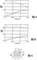
图4A,4B,4C和4D是对于图1的反应器的各种操作模式晶片表面上的刻蚀速率(竖轴)作为径向位置(横轴)的函数的视图。4A, 4B, 4C and 4D are graphs of etch rate (vertical axis) on a wafer surface as a function of radial position (horizontal axis) for various modes of operation of the reactor of FIG. 1 .
图5A,5B,5C和5D是对于图1的反应器的其他操作模式晶片表面上的刻蚀速率(竖轴)作为径向位置(横轴)的函数的视图。Figures 5A, 5B, 5C and 5D are graphs of etch rate (vertical axis) on a wafer surface as a function of radial position (horizontal axis) for other modes of operation of the reactor of Figure 1 .
图6是描绘刻蚀速率作为磁场的函数的视图。Figure 6 is a graph depicting etch rate as a function of magnetic field.
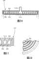
图7和8示出了具有MERIE磁体的图1A的反应器。Figures 7 and 8 show the reactor of Figure 1A with MERIE magnets.
图9描绘了操作图1A的反应器的方法。Figure 9 depicts a method of operating the reactor of Figure 1A.
图10是示出了在图1A的反应器中磁压强和离子或者电子密度作为晶片表面上的径向位置的函数的比较示例的视图。FIG. 10 is a graph showing a comparative example of magnetic pressure and ion or electron density as a function of radial position on the wafer surface in the reactor of FIG. 1A .
图11是描绘了刻蚀速率不均匀性作为线圈电流的函数的视图。Figure 11 is a graph depicting etch rate non-uniformity as a function of coil current.
图12示出了在图11的示例中在零线圈电流下的径向离子分布。FIG. 12 shows the radial ion distribution at zero coil current in the example of FIG. 11 .
图13A和13B比较了在11的示例中在约11安培的线圈电流下的测量到的和预测的刻蚀速率分布。13A and 13B compare the measured and predicted etch rate distributions in the example of 11 at a coil current of about 11 amperes.
图14A和14B比较了在11的示例中在约35安培的线圈电流下的测量到的和预测的刻蚀速率分布。14A and 14B compare the measured and predicted etch rate profiles in the example of 11 at a coil current of about 35 amps.
图15描绘了操作图1A的反应器的另一个方法。Figure 15 depicts another method of operating the reactor of Figure 1A.
图16示出了在对应于图1A的反应器中得到的磁场分布。Fig. 16 shows the magnetic field distribution obtained in the reactor corresponding to Fig. 1A.
图17描绘了图16的在晶片平面中的磁场的平方的梯度。FIG. 17 depicts the gradient of the square of the magnetic field in the plane of the wafer of FIG. 16 .
图18示出了在对应于图1A的反应器中得到的另一个磁场分布。Fig. 18 shows another magnetic field distribution obtained in the reactor corresponding to Fig. 1A.
图19描绘了图18的在晶片平面中的磁场的平方的梯度。FIG. 19 depicts the gradient of the square of the magnetic field of FIG. 18 in the plane of the wafer.
图20示出了在对应于图1A的反应器中得到的另一个磁场分布。Fig. 20 shows another magnetic field distribution obtained in the reactor corresponding to Fig. 1A.
图21描绘了图20的在晶片平面中的磁场的平方的梯度。FIG. 21 depicts the gradient of the square of the magnetic field of FIG. 20 in the plane of the wafer.
图22描绘了操作图1A的反应器的另一个方法。Figure 22 depicts another method of operating the reactor of Figure 1A.
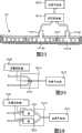
图23示出了用于控制图1A的反应器的示例性微控制器操作。Figure 23 shows an exemplary microcontroller operation for controlling the reactor of Figure 1A.
图24示出了包括图1A的反应器中所包含的特征的等离子体反应器。Figure 24 shows a plasma reactor including features included in the reactor of Figure 1A.
图25示出了包括图1A的反应器中所包含的特征的另一个等离子体反应器。Figure 25 shows another plasma reactor including features included in the reactor of Figure 1A.
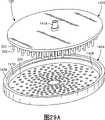
图26,27,28,29A和29B示出了用于图1A、24和25的反应器的气体分配板。Figures 26, 27, 28, 29A and 29B show gas distribution plates for the reactors of Figures 1A, 24 and 25.
图30和31示出了在如图26的气体分配板中的热控制特征。30 and 31 illustrate thermal control features in a gas distribution plate as in FIG. 26 .
图32和33示出了对应于图26的具有双区气流控制的气体分配板。Figures 32 and 33 show a gas distribution plate corresponding to Figure 26 with dual zone gas flow control.
图34示出了对应于图1A的具有双区气体分配板的等离子体反应器。Figure 34 shows a plasma reactor corresponding to Figure 1A with a dual zone gas distribution plate.
图35和36示出了示例性的双区气流控制器。35 and 36 illustrate exemplary dual zone airflow controllers.
图37示出了对应于图34的具有三个用于控制等离子体离子分布的顶置线圈的等离子体反应器。Figure 37 shows a plasma reactor corresponding to Figure 34 with three overhead coils for controlling plasma ion distribution.
图38和39分别描绘了用于产生中心低气流分布或者中心高气流分布的图26的气体分配板中的不同气体注入孔图案。38 and 39 depict different gas injection hole patterns in the gas distribution plate of FIG. 26 for producing a center low or center high gas flow distribution, respectively.
图40,41,42和43示出了用于控制等离子体离子分布的顶置线圈的不同布置。Figures 40, 41 , 42 and 43 show different arrangements of overhead coils for controlling plasma ion distribution.
图44和45示出了对应于图1A的其中顶置线圈被反应器室上方和下方的上磁性线圈和下磁性线圈代替以产生图45中可见的尖峰形磁场的等离子体反应器。44 and 45 show a plasma reactor corresponding to FIG. 1A in which the overhead coils are replaced by upper and lower magnetic coils above and below the reactor chamber to generate the spike-shaped magnetic field visible in FIG. 45 .
图46示出了如何可由可配置磁场(CMF)线圈代替图44的上和下线圈,其中以产生图45的尖峰形磁场的方式操作所述可配置磁场(CMF)线圈。FIG. 46 shows how the upper and lower coils of FIG. 44 can be replaced by configurable magnetic field (CMF) coils operated in such a way as to produce the spike-shaped magnetic field of FIG. 45 .
图47A-47D示出了图46的CMF线圈的产生所期望的磁场配置的操作模式。47A-47D illustrate the modes of operation of the CMF coil of FIG. 46 to produce the desired magnetic field configuration.
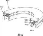
图48,49和50示出了图1A的反应器中的用于防止等离子体离子进入反应器的抽吸套环的环形孔隙板。Figures 48, 49 and 50 show the annular aperture plate of the suction collar used to prevent plasma ions from entering the reactor in the reactor of Figure IA.
图51示出了用于处理矩形工件的图1A的矩形形式的反应器。Figure 51 shows the reactor in the rectangular form of Figure IA for processing rectangular workpieces.
图52示出了对应于图1A的具有可伸缩工件支撑底座的反应器。Figure 52 shows a reactor corresponding to Figure 1A with a retractable workpiece support base.
图53A和53B示出了使用两个顶置线圈和一个下部线圈控制等离子体离子分布的不同实施例。Figures 53A and 53B show different embodiments of controlling plasma ion distribution using two overhead coils and one lower coil.
图54描绘了本发明的一个实施例。Figure 54 depicts one embodiment of the present invention.
图55A到55C描绘了在晶片平面上对应于图54的反应器的三个模式的三个磁场。55A to 55C depict three magnetic fields corresponding to the three modes of the reactor of FIG. 54 on the wafer plane.
图56A到56C分别描绘了对应于55A到55C所施加的电磁DC电流。56A to 56C depict the applied electromagnetic DC currents corresponding to 55A to 55C, respectively.
图57A和57B是分别比较了图54的反应器的尖峰模式和模式的径向分量和轴线分量的分布的视图。57A and 57B are views comparing the distribution of the spike mode and the radial and axial components of the mode, respectively, for the reactor of FIG. 54 .
图58A和58B是分别比较了图54的反应器的螺线模式和镜像模式的径向分量和轴线分量的分布的视图。58A and 58B are views comparing the distribution of the radial and axial components of the helical mode and mirror mode, respectively, of the reactor of FIG. 54 .
图59是对于图54的反应器的不同模式的等离子体离子径向分布(从离子饱和电流推导)的视图。Figure 59 is a view of the plasma ion radial distribution (derived from ion saturation current) for different modes of the reactor of Figure 54 .
图60是对于图54的不同磁场或者模式刻蚀速率作为半径的函数的视图。FIG. 60 is a graph of etch rate as a function of radius for different magnetic fields or modes of FIG. 54 .
图61描绘了通过刻蚀速率不均匀性和器件损伤来表征不同的磁场或者模式的表。Figure 61 depicts a table characterizing different magnetic fields or modes by etch rate non-uniformity and device damage.
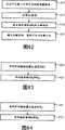
图62描绘了用于确定三个磁体中的至少两个的最优DC线圈电流的基本过程。Figure 62 depicts the basic process for determining optimal DC coil currents for at least two of the three magnets.
图63描述了可以接在图62的过程之后用于确定所有三个磁体的DC电流的附加过程。FIG. 63 describes an additional process that may follow the process of FIG. 62 for determining the DC currents for all three magnets.
图64描绘了对于图63的过程的可选替换。FIG. 64 depicts an alternative to the process of FIG. 63 .
图65是描绘了根据利用一个磁体的第一查寻对于不同磁场强度的刻蚀速率径向部分的视图。Fig. 65 is a view depicting radial sections of etch rates for different magnetic field strengths according to a first lookup with one magnet.
图66是描绘了根据利用另一个磁体的第二查寻对于不同磁场强度的刻蚀速率径向部分的视图。Figure 66 is a graph depicting the etch rate radial section for different magnetic field strengths according to a second lookup with another magnet.
图67是描绘了由图65和66的分布构建的数学分布函数的视图。FIG. 67 is a graph depicting a mathematical distribution function constructed from the distributions of FIGS. 65 and 66 .
图68描绘了用于确定最优电磁体DC电流的一个过程。Figure 68 depicts a process for determining optimal electromagnet DC current.
图69描绘了用于确定最优电磁体DC电流的另一个过程。Figure 69 depicts another process for determining optimal electromagnet DC current.
图70描绘了用于确定最优电磁体DC电流的另一个过程。Figure 70 depicts another process for determining optimal electromagnet DC current.
图71A到71E描绘了在图70的过程的后续步骤中得到的刻蚀速率分布。71A to 71E depict etch rate profiles obtained in subsequent steps of the process of FIG. 70 .
具体实施方式Detailed ways
特定等离子体反应室所展现出的等离子体离子密度分布是室压强、气体混合物和扩散、以及功率源辐射模式的函数。在本反应器中,此分布被通过磁力改变,以接近已经被预定来改善工艺均匀性的选定或者理想分布。被磁力改变或者校正的等离子体离子密度分布使得晶片或者工件表面上的工艺均匀性被改善。为此,取决于用户所确定的需求,被磁力校正的等离子体分布可以是不均匀的,或者其可以是均匀的。我们已经发现平均的磁场强度将压强施加于等离子体以改变其分布的效率可以得到提高。根据此发现,通过增大磁场梯度的径向分量可以实现此令人惊奇的结果。径向被理解为是关于圆筒形室的轴对称的。因此,所需要的是具有大的径向梯度并且沿其他方向的小场强的磁场配置。这样的磁场是其对称轴与圆筒形反应器室的轴一致的尖峰形。一种产生尖峰形磁场的方法是在圆筒形室的上方和下方提供线圈,并且使DC电流以相反的方向流过这些线圈。The plasma ion density distribution exhibited by a particular plasma reaction chamber is a function of chamber pressure, gas mixture and diffusion, and power source radiation pattern. In the present reactor, this distribution is altered magnetically to approximate a selected or ideal distribution that has been predetermined to improve process uniformity. The magnetically altered or corrected plasma ion density distribution results in improved process uniformity across the wafer or workpiece surface. For this reason, the magnetically corrected plasma distribution may be non-uniform, or it may be uniform, depending on the needs determined by the user. We have found that the average magnetic field strength can increase the efficiency with which pressure is applied to the plasma to change its distribution. According to this finding, this surprising result can be achieved by increasing the radial component of the magnetic field gradient. Radial is understood to be symmetrical about the axis of the cylindrical chamber. Therefore, what is needed is a magnetic field configuration with a large radial gradient and small field strengths in other directions. Such a magnetic field is peak-shaped with its axis of symmetry coinciding with the axis of the cylindrical reactor chamber. One way to generate a spike-shaped magnetic field is to provide coils above and below the cylindrical chamber, and to pass DC current through these coils in opposite directions.
取决于室的设计,在晶片底座的下方提供线圈可能是不现实的,因此在第一种情况中,顶部线圈足以实现这些目的。此外,所需要的是尖峰形磁场可配置或者可调节来精确控制或者改变给定等离子体反应器室中固有的等离子体离子分布(“环境”等离子体离子分布)。因为在不同的电容耦合反应器中所提供的等离子体离子分布可能变化很大,所以这样的可调节性在某些情况下可能是重要的。磁场梯度的径向分量被选择来施加将环境分布改变为期望分布所需的磁压强。例如,如果所期望的分布是均匀分布,则所施加的磁场被选择为抵消在不存在磁场的情况下反应器所展现的等离子体离子密度的径向分布的不均匀性。在此情况下,例如,如果反应器趋向于具有中心高的等离子体离子密度分布,则磁场梯度被选择来维持晶片支撑底座的中心上方的等离子体密度,并且增强周缘附近的等离子体密度以获得均匀性。Depending on the chamber design, it may not be practical to provide coils below the wafer base, so in the first case a top coil is sufficient for these purposes. Furthermore, what is needed is a spike-shaped magnetic field that is configurable or adjustable to precisely control or alter the plasma ion distribution inherent in a given plasma reactor chamber ("ambient" plasma ion distribution). Such adjustability may be important in some cases because the distribution of plasma ions provided in different capacitively coupled reactors may vary widely. The radial component of the magnetic field gradient is selected to exert the magnetic pressure required to change the ambient distribution to a desired distribution. For example, if the desired distribution is a uniform distribution, the applied magnetic field is chosen to counteract inhomogeneities in the radial distribution of plasma ion density exhibited by the reactor in the absence of a magnetic field. In this case, for example, if the reactor tends to have a centrally high plasma ion density profile, the magnetic field gradient is chosen to maintain the plasma density over the center of the wafer support pedestal and enhance the plasma density near the periphery to obtain Uniformity.
根据我们的发现通过提供至少一个第二顶置线圈可以实现这样的尖峰形磁场的可调节性,其中所述第二顶置线圈具有不同于(例如小于)第一线圈的直径。在各个线圈中的DC电流是独立可调节的,以允许以高度灵活的方式配置尖峰形磁场,来实质改变任何环境等离子体离子密度,以便使其接近某种所期望的等离子体离子密度。这样的场配置选择可以被设计来改进中心高或者中心低的等离子体离子密度分布。Such adjustability of the spike-shaped magnetic field can be achieved according to our findings by providing at least one second overhead coil having a different (eg smaller) diameter than the first coil. The DC current in each coil is independently adjustable to allow the spike-shaped magnetic field to be configured in a highly flexible manner to alter virtually any ambient plasma ion density so as to approach some desired plasma ion density. Such field configuration choices can be designed to improve either center-high or center-low plasma ion density distributions.
可以实现的一个优点是两方面的,因为尖峰形磁场具有相对于磁场强度的大的径向梯度(如上所述),因此对于对等离子体施加校正压强是高效的;但是,因为磁场随时间是恒定的,所以产生电弧放电的趋势大大减小,因此当需要时可以使用更强一点的磁场,以获得甚至更大的校正能力。如将在此说明书中稍后所描述的,此特征在较高的室压强下可能是非常有用的。One advantage that can be realized is two-fold, because the spike-shaped magnetic field has a large radial gradient with respect to the magnetic field strength (as described above), and is therefore efficient for applying corrective pressure to the plasma; however, because the magnetic field is Constant, so the tendency to arc is greatly reduced, so a slightly stronger magnetic field can be used when required for even greater corrective capability. This feature may be very useful at higher chamber pressures, as will be described later in this specification.
图1A示出了能够提供可调节尖峰形磁场的电容耦合等离子体反应器。图1A的反应器包括圆筒形侧壁5、作为气体分配板的顶板10以及支持半导体工件20的晶片支撑底座15。顶板10或者气体分配板可以是导电的,以使其可以充当阳极或者其可以具有安装到其上的阳极。顶板10或者气体分配板一般由铝制成,并且具有内部气体歧管并且在其面对室中的内部表面中具有气体注入口。处理气体源25将处理气体供应到气体分配板10。真空泵30控制反应器室内的压强。用于激发和维持反应器室内的等离子体的等离子体功率源通过RF发生器40来产生,所述RF发生器40通过阻抗匹配电路45连接到晶片支撑底座15,以使晶片支撑底座充当RF电极。阳极(其可以是由导体材料形成的顶板10)被连接到RF地,以充当反电极。这样的反应器往往具有非常不均匀的等离子体离子密度分布,该分布一般是中心高的。Figure 1A shows a capacitively coupled plasma reactor capable of providing an adjustable spike-shaped magnetic field. The reactor of FIG. 1A comprises a
图1B示出了其中顶板10通过RF阻抗匹配元件11(仅仅示意性地示出)连接到供应等离子体功率源的VHF信号发生器12,而不是如图1A中那样直接连接到地的特征。在此情况下,RF发生器40仅仅控制半导体晶片或者工件20上的偏压。(RF阻抗匹配元件11可以是诸如同轴调谐短棒或者带线电路的固定调谐元件。)在本说明书中的后面部分中将更详细地讨论这一特征。Figure 1B shows a feature where the
为了控制等离子体离子密度的分布,一组感应线圈被提供在顶板10上方。在图1A的情形中,该组线圈包括内线圈60和外线圈65,内线圈60和外线圈65与圆筒形室同轴,并且各自包含一圈导体。虽然在图1A中所示的线圈60,65为一匝,但是它们中的每一个可以包含垂直布置的多匝,例如如图1B所示。或者,如图1C所示,线圈60,65可以垂直和水平延伸。在图1A中的情形中,内线圈60的位置比外线圈65更远离顶板10的上方。但是,在其他情形中,此布置可以被反过来,或者两个线圈60,65可以处在顶板10上方相同的高度上。In order to control the distribution of plasma ion density, a set of induction coils is provided above the
在图1A和1B的情形中,控制器90通过控制分别连接到线圈60,65的各自独立的DC电流源70,75,来确定流到各个顶置的线圈60,65的电流的大小和极性。现在参考图2,示出了这样的情形,其中控制器90控制从DC电流源76到线圈60,65的DC电流,所述DC电流源76通过控制器90供应电流,控制器90被分别连接到线圈60,65中的每一个。在这两种情形中,控制器90都能够使得不同极性和大小的DC电流分别在线圈60,65中流动。在图2的情形中,控制器90包括一对电位计82a、82b和一对联动开关84a,84b,所述电位计82a、82b调节施加到各个线圈60,65的DC电流,所述联动开关84a,84b独立地确定施加到每一个线圈60,65的DC电流的极性。诸如微处理器91之类的可编程设备可以被包括在控制器90中,以便智能地控制电位计82a、82b和联动开关84a,84b。In the situation of FIGS. 1A and 1B, the
图1A,1B和1C中所示的其中内线圈60比外线圈65布置在顶板10上方更高的高度上的两个线圈60,65的布置,提供了某些优点。具体地,由各个线圈提供的磁场梯度的径向分量至少是大致与线圈的半径成正比,与离线圈的轴向位移成反比。因此,内线圈60和外线圈65因为其不同的尺寸和位移将起到不同的作用:外圈65将主导晶片20的整个表面,因为其半径更大并且更靠近晶片20,而内线圈60将在晶片中心附近有最大的影响,并且可以被看作用于更精细调节或者调控磁场的调整线圈。其他布置也可以用于实现这样的通过具有不同的半径和布置在离等离子体不同的位移处的不同线圈的差别控制。如参考某些加工示例在本申请中后面所描述的,通过不仅选择在各个顶置的线圈60,65中流动的电流的不同大小,并且通过选择对于不同的顶置线圈60,65的电流的不同极性或者方向,获得了对环境等离子体离子密度分布的不同改变。The arrangement of the two
图3A示出了在图1A的情形中,作为晶片20上的径向位置的函数的由内线圈60产生的磁场的径向(实线)和方位角向(虚线)分量。图3B示出了作为晶片20上的径向位置的函数的由外线圈65产生的磁场的径向(实线)和方位角向(虚线)分量。在图3A和3B中示出的数据是在其中晶片20的直径为300mm,内线圈60的直径为12英寸并且布置在等离子体上方10英寸处,以及外线圈65的直径为22英寸并且布置在等离子体上方约6英寸处的实施方式中得到的。图3C是由内顶置线圈60和外顶置线圈65产生的半尖峰形磁场线图案的简化图。FIG. 3A shows the radial (solid line) and azimuthal (dashed line) components of the magnetic field generated by
图2的控制器90可以改变施加到各个线圈60,65的电流,以便调节晶片表面上的磁场,并由此改变等离子体离子密度的空间分布。现在将被示出的是由线圈60,65中不同一个所施加的不同磁场效应,以便说明控制器90通过改变这些磁场可以多大程度地影响和改善室中的等离子体离子密度。在下面的示例中,直接测量晶片表面上的刻蚀速率的空间分布,而不是等离子体离子分布。刻蚀速率分布直接随等离子体离子分布变化而变化,因此其中之一的变化反映了另一个的变化。The
图4A,4B,4C和4D示出了在低室压强(30mT)下只使用内线圈60所实现的有益效果。图4A示出了作为晶片20表面上的位置(水平X和Y轴)的函数的所测量到的刻蚀速率(垂直Z轴)。图4A由此示出了刻蚀速率在晶片表面的平面中的空间分布。在图4A中可清楚看到刻蚀速率分布的中心高不均匀性。图4A对应于其中没有施加磁场的情形,因此示出了在反应器中固有的并且需要校正的不均匀的刻蚀速率分布。在此情形中,刻蚀速率具有5.7%的标准偏差。在图4和5中,磁场强度将被描述为在晶片中心附近的轴向场,但是应该理解,径向场是对等离子体离子密度的径向分布起作用以改善均匀性的磁场。在本说明书中选择了轴向场,因为其更容易测量。在晶片边缘处的径向场一般是在此位置处的轴向场的1/3。Figures 4A, 4B, 4C and 4D illustrate the beneficial effect achieved using only the
图4B示出了当内线圈60已经被激励以产生9高斯的磁场时刻蚀速率分布如何变化。不均匀性减小到4.7%的标准偏差。Figure 4B shows how the etch rate distribution changes when the
在图4C中,内线圈60的磁场已经增大到18高斯,并且可以看到在中心处的峰已经大大地减小,结果晶片上的刻蚀速率标准偏差减小到2.1%。In Figure 4C, the magnetic field of the
在图4D中,内线圈60的磁场已经被进一步增大到27高斯,因此图4A的中心高的图案已经几乎被反转为中心低的图案。在图4D的情形中的晶片表面上的刻蚀速率标准偏差为5.0%。In FIG. 4D, the magnetic field of the
图5A,5B,5C和5D示出了在较高室压强(200mT)下使用线圈60,65两者的有益效果。图5A对应于图4A,并且描绘了没有通过磁场校正的反应器的中心高刻蚀速率的不均匀性。在此情形中,晶片表面上的刻蚀速率的标准偏差为5.2%。Figures 5A, 5B, 5C and 5D illustrate the benefit of using both
在图5B中,外线圈65已经被激励以产生22高斯的磁场,这在一定程度上减小了刻蚀速率分布中的中心峰。在此情形中,刻蚀速率标准偏差已经减小到3.5%。In Figure 5B, the
在图5C中,两个线圈60,65都被激励以产生24高斯的磁场。在图5C中所见的结果是刻蚀速率分布中的中心峰已经明显减小,而周缘附近的刻蚀速率已经增大。总的效果是具有3.2%的低标准偏差的更均匀的刻蚀速率分布。In Figure 5C, both
在图5D中,两个线圈都被激励,以产生40高斯的磁场,发生了过校正,因此晶片表面上的刻蚀速率分布已经转变为中心低分布。在该后一情形中的刻蚀速率标准偏差已经轻微上升(相对于图5C的情形)到3.5%。In Figure 5D, both coils are energized to produce a magnetic field of 40 Gauss, overcorrection has occurred so that the etch rate distribution on the wafer surface has shifted to a centrally low distribution. The etch rate standard deviation in this latter case has risen slightly (relative to the case of FIG. 5C ) to 3.5%.
比较在图4A-4D的低压强测试中与图5A-5D中的高压强测试中所得到的结果,可以看到较高的室压强需要大得多的磁场,以获得对刻蚀速率不均匀性分布的相似校正。例如,在30mT下,仅仅使用18高斯下的内线圈60,就获得最优校正,而在300mT下,需要使用线圈60,65两者的24高斯的磁场来获得最优校正。Comparing the results obtained in the low pressure test of Figures 4A-4D with the high pressure test in Figures 5A-5D, it can be seen that the higher chamber pressure requires a much larger magnetic field to obtain a non-uniform response to the etch rate. similarity correction for the sex distribution. For example, at 30 mT, optimal correction is obtained using only the
图6示出了顶置线圈的磁场明显影响等离子体离子密度或者刻蚀速率分布的均匀性,但是不明显影响刻蚀速率本身。这是有利的,因为虽然理想的是改善刻蚀速率分布的均匀性,但是优选的是不改变为特定半导体工艺所选定的刻蚀速率。在图6中,菱形符号描绘了作为磁场(水平轴)的函数的测量到的刻蚀速率(左手侧竖轴),而正方形符号描绘了作为磁场的函数的刻蚀速率的标准偏差(不均匀性) (右手侧竖坐标)。在所示范围内的不均匀性变化为约1个数量级,而刻蚀速率的变化仅为约25%。FIG. 6 shows that the magnetic field of the overhead coil significantly affects the plasma ion density or the uniformity of the etch rate distribution, but does not significantly affect the etch rate itself. This is advantageous because while it is desirable to improve the uniformity of the etch rate distribution, it is preferable not to alter the etch rate selected for a particular semiconductor process. In Figure 6, the diamond symbols plot the measured etch rate (left-hand vertical axis) as a function of the magnetic field (horizontal axis), while the square symbols plot the standard deviation of the etch rate as a function of the magnetic field (inhomogeneous sex) (vertical coordinates on the right-hand side). The variation in non-uniformity over the range shown is about 1 order of magnitude, while the variation in etch rate is only about 25%.
图1A,1B和1C的顶置线圈感应器60,65可以用于常规的MERIE反应器。图7和8示出了对应于图1A的具有四个常规MERIE电磁体92,94,96,98和MERIE电流控制器99的附加特征的情形。电流控制器99向各个MERIE电磁体92,94,96,98提供AC电流。各个电流具有相同的低频,但是其相位偏移量为90度,以便以常规的方法在室内产生缓慢旋转的磁场。The
利用顶置线圈控制等离子体分布Controlling plasma distribution with overhead coils
根据反应器的方法,在特定反应器中固有的晶片表面上的等离子体离子密度通过选择由顶置线圈60,65所产生的特定磁场以特定的方式被设计。例如,等离子体分布可以被设计为在晶片表面上产生更均匀的刻蚀速率分布。例如,通过对控制器90编程以选择在顶置线圈中流动的DC电流的最优极性和幅值,来实现此设计。虽然本示例涉及具有仅仅两个同心的顶置线圈(即线圈60和65)的反应器,但是该方法可以用多于两个的线圈来实现,并且可以利用更多数量的顶置线圈提供更精确的结果。磁场被控制器90设计,以改变晶片表面上的等离子体离子密度分布,这反过来影响刻蚀速率分布。Depending on the reactor approach, the plasma ion density on the wafer surface inherent in a particular reactor is designed in a particular way by selecting a particular magnetic field generated by the overhead coils 60,65. For example, the plasma distribution can be engineered to produce a more uniform etch rate distribution across the wafer surface. This design is achieved, for example, by programming the
第一步是在不存在任何来自顶置线圈60,65的校正磁场的情况下测量晶片表面上的刻蚀速率分布。下一个步骤是确定使得刻蚀速率分布更均匀的等离子体离子密度分布的变化。最后的步骤是确定将产生所期望的等离子体离子密度分布变化的磁场。在给定该磁场的情况下,产生这样的磁场所需的顶置线圈60,65中的电流的大小和方向可以由已知的静态磁场方程计算出。The first step is to measure the etch rate distribution on the wafer surface in the absence of any corrective magnetic field from the overhead coils 60,65. The next step is to determine the change in plasma ion density distribution that makes the etch rate distribution more uniform. The final step is to determine the magnetic field that will produce the desired change in plasma ion density distribution. Given this magnetic field, the magnitude and direction of the current in the overhead coils 60, 65 required to generate such a magnetic field can be calculated from known static magnetic field equations.
我们已经发现由磁场计算由顶置线圈60,65施加在等离子体上的压强(所谓的“磁压强”)的方法。这将在下面讨论。作用在等离子体上的磁压强产生等离子体离子密度分布的变化。此等离子体离子密度分布的变化产生可以被直接观察到的晶片表面上的刻蚀速率分布的正比变化。晶片表面上的等离子体离子密度分布和刻蚀速率分布因此通过比例因子至少大致相关。We have found a way to calculate the pressure exerted on the plasma by the overhead coils 60, 65 (the so-called "magnetic pressure") from the magnetic field. This will be discussed below. Magnetic pressure acting on the plasma produces changes in the ion density distribution of the plasma. Changes in this plasma ion density distribution produce proportional changes in the etch rate distribution on the wafer surface that can be directly observed. The plasma ion density distribution and etch rate distribution on the wafer surface are thus at least approximately related by a scaling factor.
首先,在从顶置线圈60,65施加磁场之前测量晶片表面上的刻蚀速率的空间分布。由此,可以确定所期望的刻蚀速率分布变化(以获得均匀的分布)。接着,由各个线圈的几何形状解析确定作为室内的位置和线圈中流动的电流的函数的由各个顶置线圈60,65产生的磁场空间分布。然后,通过向线圈施加已知的一组电流,随后测量晶片表面上的所得刻蚀速率分布变化,可以推导出线性比例因子,该比例因子将在晶片表面上来自所有线圈的磁场的矢量和与在晶片表面处的刻蚀速率分布变化相关联。(此比例因子一般是等离子体的中性压强的函数并且最高到约500mT室压强有效。)因此,在给定所期望的刻蚀速率分布变化或者校正(以获得更好的均匀性)的情况下,可以(以在本说明书中稍后所描述的方式)找出所需的磁场,并且由此利用先前解析确定的磁场空间分布函数可以推断出相应的线圈电流。First, the spatial distribution of the etch rate on the wafer surface is measured before the magnetic field is applied from the overhead coils 60,65. From this, the desired change in etch rate distribution (to obtain a uniform distribution) can be determined. Next, the spatial distribution of the magnetic field produced by each
所期望的刻蚀速率分布不均匀性校正可以以各种方法来确定。例如,可以从均匀或者平均刻蚀速率中减去晶片表面上的2维刻蚀速率分布,以产生“差分”分布。在此方法中将被校正的刻蚀速率分布的不均匀性为反应器室中各种因素的结果,这些因素包括电容耦合功率源的不均匀施加、不均匀的处理气体分布以及不均匀的等离子体离子密度分布。在前述的方法中,通过由磁压强来改变等离子体离子密度分布来校正不均匀性。The desired etch rate distribution non-uniformity correction can be determined in various ways. For example, the 2-dimensional etch rate distribution on the wafer surface can be subtracted from the uniform or average etch rate to produce a "differential" distribution. The non-uniformity of etch rate distribution to be corrected in this method is the result of various factors in the reactor chamber, including non-uniform application of capacitively coupled power sources, non-uniform process gas distribution, and non-uniform plasma Bulk ion density distribution. In the foregoing method, the inhomogeneity is corrected by changing the plasma ion density distribution by the magnetic pressure.
下面的方法也可以被用来确定以所期望的方式不均匀的“经校正”的等离子体分布。在此情形中,将进行的校正为“未校正”或者环境等离子体离子密度分布和所期望的分布(其本身是不均匀的)的差。因此,该方法对于产生或者更加均匀或者具有不必是均匀的特意选定的密度分布模式的等离子体密度分布是有用的。The following method can also be used to determine a "corrected" plasma distribution that is not uniform in a desired manner. In this case, the correction to be made is "uncorrected" or the difference between the ambient plasma ion density distribution and the desired distribution (which is itself inhomogeneous). Thus, the method is useful for producing plasma density distributions that are either more uniform or have a deliberately selected density distribution pattern that is not necessarily uniform.
现在将参考图9描述用于实现前述方法的一系列步骤。A series of steps for implementing the aforementioned method will now be described with reference to FIG. 9 .
第一步(图9的方框910)是对于顶置线圈60,65中的每一个解析确定作为线圈中流动的电流和晶片表面上的径向位置的函数的晶片表面处的磁场的表达式。使用柱坐标,对于第i个线圈,该表达式可以被写为Bi(r,z=晶片,Ii)。其由毕奥一萨伐(Biot-Savart)定律以非常直接的方式确定。The first step (block 910 of FIG. 9) is to analytically determine, for each of the overhead coils 60, 65, an expression for the magnetic field at the wafer surface as a function of the current flowing in the coil and the radial position on the wafer surface . Using cylindrical coordinates, for the ith coil, this expression can be written as Bi (r, z=wafer, Ii ). It is determined in a very straightforward manner by the Biot-Savart law.
下一步(图9中的方框920)是在顶置线圈60,65中没有电流流动的情况下进行。在此步骤中,测量晶片表面上等离子体离子密度的空间分布。此空间分布可以被写为n(r,z=晶片)。在此步骤中,可以通过测量测试晶片的表面上的刻蚀速率分布间接地测量等离子体离子密度分布。技术人员可以从刻蚀速率分布容易地推断出等离子体离子密度分布。The next step (block 920 in FIG. 9 ) is performed with no current flowing in the overhead coils 60 , 65 . In this step, the spatial distribution of the plasma ion density on the wafer surface is measured. This spatial distribution can be written as n(r, z=wafer). In this step, the plasma ion density distribution can be indirectly measured by measuring the etching rate distribution on the surface of the test wafer. A skilled person can easily deduce the plasma ion density distribution from the etch rate distribution.
接着,在方框930的步骤中,确定对在前面的步骤中所测量到的测量等离子体离子密度空间分布函数n(r,z=晶片)的校正c(r)。校正c(r)可以以任何合适方式定义。例如,其可以被定义为最大值n(r,z=晶片)max减去n(r,z=晶片)。在此方式中,将c(r)加到n(r,z=晶片)产生“经校正”的分布,其具有等于n(r)max的均匀幅值。当然,可以定义不同的校正函数c(r),以产生不同的均匀幅值。或者,如上面简要提及的,如果所期望的分布是不均匀的,则该校正为所期望的分布和n(r,z=晶片)之间的差。Next, in a block 930 step, a correction c(r) to the measured plasma ion density spatial distribution function n(r, z=wafer) measured in the previous step is determined. The correction c(r) can be defined in any suitable way. For example, it may be defined as the maximum value n(r,z=wafer)max minus n(r,z=wafer). In this manner, adding c(r) to n(r, z=wafer) produces a "corrected" distribution with a uniform magnitude equal to n(r)max . Of course, different correction functions c(r) can be defined to produce different uniform amplitudes. Alternatively, as mentioned briefly above, if the desired distribution is non-uniform, the correction is the difference between the desired distribution and n(r, z=wafer).
下一步(方框940)是为顶置线圈60,65中的每一个选择“测试”电流Ii,并且将该电流施加到相应的线圈,并测量所得的等离子体离子分布,其可以被写为n(r,z=晶片)test。通过将在具有和没有磁场情况下测量到的离子分布相减,得到离子分布变化Δn(r):The next step (block 940) is to select a "test" currentIi for each of the overhead coils 60, 65, and apply this current to the corresponding coil, and measure the resulting plasma ion distribution, which can be written is n(r, z=wafer)test . The ion distribution change Δn(r) is obtained by subtracting the ion distribution measured with and without the magnetic field:
Δn(r)≈n(r,z=晶片)-n(r,z=晶片)testΔn(r)≈n(r, z=chip)-n(r, z=chip)test
下一步(方框950)是计算将由磁场施加的压强(即,磁压强)梯度与离子分布变化Δn(r)相关联的比例因子S。此计算通过将磁压强梯度除以Δn(r)来完成。根据下面的磁-流体动力学方程,对于每一个线圈分别计算第i个线圈的磁场B(r,z=晶片,Ii)的磁压强梯度:The next step (block 950) is to calculate the scaling factor S that relates the pressure (ie, magnetic pressure) gradient imposed by the magnetic field to the ion distribution change Δn(r). This calculation is done by dividing the magnetic pressure gradient by Δn(r). According to the following magneto-hydrodynamic equation, the magnetic pressure gradient of the i-th coil's magnetic field B (r, z=chip, Ii ) is calculated for each coil:
▽rP≈-▽r[B(r,z=晶片,Ii)2/2μ0]▽r P≈-▽r [B(r, z=wafer, Ii )2 /2μ0 ]
其中,下标r表示径向分量。对于每一个线圈分别如此得到的结果然后被加和起来。因此,总的磁压强梯度为:Among them, the subscript r indicates the radial component. The results thus obtained separately for each coil are then added up. Therefore, the total magnetic pressure gradient is:
-▽r{∑i[B(r,z=晶片,Ii)2/2μ0]}-▽r {∑i [B(r, z=chip, Ii )2 /2μ0 ]}
因此,比例因子S为:Therefore, the scaling factor S is:
S={-▽r{∑i[B(r,z=晶片,Ii)2/2μ0]}}/Δn(r)S={-▽r {∑i [B(r, z=wafer, Ii )2 /2μ0 ]}}/Δn(r)
此除法操作可以在r的不同值处执行并且结果被平均以获得标量形式的S。否则,比例因子S将是r的函数并且以适当的方式被使用。This division operation can be performed at different values of r and the results averaged to obtain S in scalar form. Otherwise, the scaling factor S will be a function of r and used in an appropriate manner.
在方框940的步骤中得到的比例因子S是确定磁压强的线圈电流Ii和离子分布中的所得变化之间的联系量。特别地,在给定一组线圈电流Ii的情况下,通过将从该组Ii确定的磁压强除以比例因子S可以计算出离子分布n(r)中的相应变化:The scaling factor S obtained in the step of block 940 is the quantity that determines the link between the coil current Ii of the magnetic pressure and the resulting change in ion distribution. In particular, given a set of coil currentsIi , the corresponding change in ion distribution n(r) can be calculated by dividing the magnetic pressure determined from this setIi by the scaling factor S:
Δn(r)={-▽r{∑i[B(r,z=晶片,Ii)2/2μ0]}}/SΔn(r)={-▽r {∑i [B(r, z=wafer, Ii )2 /2μ0 ]}}/S
此事实提供了后续步骤(方框960)的基础,在后续步骤中计算机(例如微处理器91)使用上述等式来查寻对等离子体离子密度分布的上述指定或期望变化Δn(r)产生最优近似的一组线圈电流Ii。在此情况下,期望变化等于在方框930的步骤中计算的校正函数c(r)。换言之,计算机查寻满足以下条件的一组线圈电流Ii:This fact provides the basis for the subsequent step (block 960) in which a computer (e.g., microprocessor 91) uses the above equation to find the most A good approximation of a set of coil currents Ii . In this case, the desired change is equal to the correction function c(r) calculated in the step of block 930 . In other words, the computer looks for a set of coil currents Ii that satisfy the following conditions:
{-▽r{∑i[B(r,z=晶片,Ii)2/2μ0]}}=c(r)S{-▽r {∑i [B(r, z=chip, Ii )2 /2μ0 ]}}=c(r)S
此查寻可以通过包括例如最速下降法的公知最优化技术来实现。本领域技术人员容易实施该技术,并且无需在此描述。This search can be accomplished by well-known optimization techniques including, for example, steepest descent. This technique is readily implemented by those skilled in the art and need not be described here.
然后将由查寻发现的该组电流Ii的大小和极性发送到控制器90,控制器90反过来将这些电流施加到各个线圈60,65。The magnitude and polarity of the set of currents Ii found by the lookup are then sent to the
图10比较了磁压强(实线)与测量到的等离子体离子分布(其作为晶片表面上的径向位置的函数)的变化(虚线)。如上所讨论的,磁压强是顶置线圈的磁场的平方的梯度。图10表明在磁压强和离子密度分布的变化之间存在良好的相关性。Figure 10 compares the change in magnetic pressure (solid line) to the measured plasma ion distribution as a function of radial position on the wafer surface (dashed line). As discussed above, the magnetic pressure is the gradient of the square of the magnetic field of the overhead coil. Figure 10 shows that there is a good correlation between changes in magnetic pressure and ion density distribution.
在图11-14中示出了这样的方法的应用。图11示出了在晶片表面处的刻蚀速率空间分布的不均匀性或者标准偏差(竖轴)如何随顶置线圈之一中的线圈电流变化。在零线圈电流下,标准偏差为约12%,并且离子分布为中心高的分布,如图12所示。The application of such a method is shown in Figures 11-14. Figure 11 shows how the inhomogeneity or standard deviation (vertical axis) of the etch rate spatial distribution at the wafer surface varies with coil current in one of the overhead coils. At zero coil current, the standard deviation is about 12%, and the ion distribution is a center-high distribution, as shown in FIG. 12 .
在约17安培的线圈电流下,获得约3%的最小不均匀性。这表示改善了约4倍(即,刻蚀速率分布的12%改善到3%的标准偏差)。实际或者测量到的刻蚀速率分布如图13A所示,而使用图9的技术所预测的刻蚀速率分布如图13B所示。At a coil current of about 17 amps, a minimum non-uniformity of about 3% was obtained. This represents an improvement by a factor of about 4 (ie, a 12% improvement to a 3% standard deviation of the etch rate distribution). The actual or measured etch rate distribution is shown in Figure 13A, while the etch rate distribution predicted using the technique of Figure 9 is shown in Figure 13B.
在35安培的高线圈电流下,刻蚀速率分布标准偏差为约14%。所测量到的刻蚀速率空间分布被示于图14A中,而预测的分布如图14B所示。At a high coil current of 35 amps, the etch rate distribution standard deviation was about 14%. The measured etch rate spatial distribution is shown in Figure 14A, while the predicted distribution is shown in Figure 14B.
再次参考图13A,所获得的最均匀的离子分布肯定不是平坦的,并且事实上具有“碗状”形状,其在周缘附近是凹入的并在中心附近是凸起的。利用更多数量的独立顶置线圈(例如,三个或者更多个)、以更大分辨率和更好均匀性的结果进行电流最优化是可以的。因此,反应器不限于具有仅仅两个线圈的情形。可以利用小于或者大于两个的顶置线圈以不同的结果来实现反应器。Referring again to Figure 13A, the most uniform ion distribution obtained is certainly not flat, and in fact has a "bowl-like" shape that is concave near the periphery and convex near the center. It is possible to perform current optimization with a greater number of individual overhead coils (eg, three or more), with greater resolution and better uniformity of results. Thus, the reactor is not limited to having only two coils. Reactors can be realized with less or more than two overhead coils with varying results.
可以应用相同的方法以便控制在顶板表面处的等离子体离子密度分布或者刻蚀速率分布。例如,这样的方法在室清洁操作过程中可能是有用的。图15示出了图9的方法的一个方案,其中离子密度(或者刻蚀速率)的空间分布的均匀性被最优化。图15的步骤,即方框910’,920’,930’,940’,950’和960’与图9的步骤,即方框方框910,920,930,940,950和960相同,不同之处在于图15的步骤是针对顶板平面而不是晶片平面进行的:The same approach can be applied in order to control the plasma ion density distribution or etch rate distribution at the top plate surface. For example, such an approach may be useful during chamber cleaning operations. FIG. 15 shows a version of the method of FIG. 9 in which the uniformity of the spatial distribution of ion density (or etch rate) is optimized. The steps of Fig. 15, i.e. blocks 910', 920', 930', 940', 950' and 960' are the same as the steps of Fig. 9, i.e. blocks 910, 920, 930, 940, 950 and 960, different The difference is that the steps of Figure 15 are performed for the top plate plane rather than the wafer plane:
第一步(图15的方框910’)是对于顶置线圈60,65中的每一个解析确定作为线圈中流动的电流和晶片表面上的径向位置的函数的顶板表面处的磁场的表达式。使用柱坐标,对于第i个线圈,该表达式可以被写为Bi(r,z=顶板,Ii)。其由简单的静态磁场方程确定,并且不仅是线圈电流Ii和顶板表面上的径向位置r的函数而且是某些常数诸如线圈的半径和线圈和顶板内表面之间的距离,z=顶板的函数。The first step (block 910' of FIG. 15) is to analytically determine, for each of the overhead coils 60, 65, an expression of the magnetic field at the top plate surface as a function of the current flowing in the coil and the radial position on the wafer surface Mode. Using cylindrical coordinates, for the ith coil, this expression can be written as Bi (r, z = top plate, Ii ). It is determined by a simple static magnetic field equation and is not only a function of the coil currentIi and the radial position r on the top plate surface but also some constants such as the radius of the coil and the distance between the coil and the inner surface of the top plate, z = top plate The function.
下一步(图15中的方框920’)是在顶置线圈60,65中没有电流流动的情况下进行。在此步骤中,测量顶板表面上等离子体离子密度的空间分布。此空间分布可以被写为n(r,z=顶板)。在此步骤中,可以通过常规的探测或者其他间接的技术测量等离子体离子密度分布。The next step (block 920' in Figure 15) is performed with no current flowing in the overhead coils 60,65. In this step, the spatial distribution of the plasma ion density on the surface of the top plate is measured. This spatial distribution can be written as n(r, z = top plate). In this step, the plasma ion density distribution can be measured by conventional probing or other indirect techniques.
接着,在方框930’的步骤中,确定对在前面的步骤中所测量到的测量等离子体离子密度空间分布函数n(r,z=顶板)的校正c’(r)。(应该注意在此使用撇号’来区分图15的计算与上述图9的计算,并且该撇号’不表示在本文中所使用的导数。)校正c’(r)可以以任何合适方式定义。例如,其可以被定义为最大值n(r,z=顶板)max减去n(r,z=顶板)。在此方式中,将c’(r)加到n(r,z=顶板)产生“经校正”的分布,其具有等于n(r)max的均匀幅值。当然,可以定义不同的校正函数c’(r),以产生不同的均匀幅值。同样,如果期望特定的不均匀分布,则该校正为未校正或者环境等离子体分布n(r,z=顶板)和所期望的不均匀分布之间的差。这样,该方法可以用于建立或者所期望的具有特定不均匀图案的等离子体离子分布或者建立均匀等离子体离子密度分布。Next, in a block 930' step, a correction c'(r) to the measured plasma ion density spatial distribution function n(r, z=top plate) measured in the previous step is determined. (It should be noted that the prime '' is used here to distinguish the calculation of FIG. 15 from the calculation of FIG. 9 above, and that the prime ' does not denote the derivative as used herein.) The correction c'(r) may be defined in any suitable way . For example, it can be defined as the maximum value n(r,z=top plate)max minus n(r,z=top plate). In this manner, adding c'(r) to n(r, z=top plate) produces a "corrected" distribution with a uniform magnitude equal to n(r)max . Of course, different correction functions c'(r) can be defined to produce different uniform amplitudes. Likewise, if a specific non-uniform distribution is desired, the correction is the difference between the uncorrected or ambient plasma distribution n (r, z = ceiling) and the desired non-uniform distribution. As such, the method can be used to create either a desired plasma ion distribution with a particular non-uniform pattern or to create a uniform plasma ion density distribution.
下一步(方框940’)是为顶置线圈60,65中的每一个选择“测试”电流Ii,并且将该电流施加到相应的线圈,并测量所得的等离子体离子分布,其可以被写为n(r,z=顶板)test。通过将在具有和没有磁场情况下测量到的离子分布相减,得到离子分布变化Δn’(r):The next step (block 940') is to select a "test" current Ii for each of the overhead coils 60, 65 and apply this current to the corresponding coil and measure the resulting plasma ion distribution, which can be determined by Write n(r, z=top plate)test . The ion distribution change Δn'(r) is obtained by subtracting the ion distribution measured with and without the magnetic field:
Δn’(r)=n(r,z=顶板)-n(r,z=顶板)testΔn'(r)=n(r, z=top plate)-n(r, z=top plate)test
下一步(方框950’)是计算将由磁场施加的压强(即,磁压强)梯度与离子分布变化Δn’(r)相关联的比例因子S’。此计算通过将磁压强梯度除以Δn’(r)来完成。根据磁-流体动力学方程,对于每一个线圈分别计算第i个线圈的磁场B(r,z=顶板,Ii)的磁压强梯度:The next step (block 950') is to calculate the scaling factor S' relating the pressure (ie, magnetic pressure) gradient applied by the magnetic field to the ion distribution change Δn'(r). This calculation is done by dividing the magnetic pressure gradient by Δn'(r). According to the magneto-hydrodynamic equation, the magnetic pressure gradient of the i-th coil's magnetic field B (r, z=top plate, Ii ) is calculated for each coil:
▽rP=-▽r[B(r,z=顶板,Ii)2/2μ0]▽r P=-▽r [B(r, z=top plate, Ii )2 /2μ0 ]
其中,下标r表示径向分量。对于每一个线圈分别如此得到的结果然后被加和起来。因此,总的磁压强梯度为:Among them, the subscript r indicates the radial component. The results thus obtained separately for each coil are then added up. Therefore, the total magnetic pressure gradient is:
-▽r{∑i[B(r,z=顶板,Ii)2/2μ0]}-▽r {∑i [B(r, z=top plate, Ii )2 /2μ0 ]}
因此,比例因子S为:Therefore, the scaling factor S is:
S’={-▽r{∑i[B(r,z=顶板,Ii)2/2μ0]}}/Δn’(r)S'={-▽r {∑i [B(r, z=top plate, Ii )2 /2μ0 ]}}/Δn'(r)
在方框950’的步骤中找出的比例因子S’是确定磁压强的线圈电流Ii和所得的离子分布变化之间的联系量。具体来说,在给定一组线圈电流Ii的情况下,相应的离子分布的变化Δn’(r)可以通过将由该组电流Ii所确定的磁压强除以比例因子S’计算出:The scaling factor S' found in the step of block 950' is the quantity that determines the link between the coil current Ii of the magnetic pressure and the resulting change in ion distribution. Specifically, given a set of coil currents Ii , the corresponding change in ion distribution Δn'(r) can be calculated by dividing the magnetic pressure determined by the set of currents Ii by the scaling factor S':
Δn’(r)={-▽r{∑i[B(r,z=顶板,Ii)2/2μ0]}}/S’Δn'(r)={-▽r {∑i [B(r, z=top plate, Ii )2 /2μ0 ]}}/S'
该事实为下面的步骤(方框960’)提供了基础,在该步骤中,计算机(例如微处理器91)使用前述的方程查寻一组线圈电流Ii,该组线圈电流Ii对于先前指定的或者所期望的等离子体离子密度分布的变化Δn’(r)产生最优近似。在此情况下,所期望的变化等于在方框930’的步骤中计算出的校正函数c’(r)。换句话说,计算机查寻一组满足下面的条件的线圈电流Ii:This fact provides the basis for the following step (block 960') in which the computer (e.g., microprocessor 91) uses the aforementioned equations to look up a set of coil currents Ii for whicha previously specified The variation Δn'(r) of the desired or desired plasma ion density distribution yields an optimal approximation. In this case, the desired change is equal to the correction function c'(r) calculated in the step of block 930'. In other words, the computer looks for a set of coil currents Ii that satisfy the following conditions:
{-▽r{∑i[B(r,z=顶板,Ii)2/2μ0]}}=c’(r)S’{-▽r {∑i [B(r, z=top plate, Ii )2 /2μ0 ]}}=c'(r)S'
此查寻可以通过包括例如最速下降法的公知最优化技术来实现。本领域技术人员容易实施该技术,并且无需在此描述。This search can be accomplished by well-known optimization techniques including, for example, steepest descent. This technique is readily implemented by those skilled in the art and need not be described here.
然后将由查寻发现的该组电流Ii的大小和极性发送到控制器90,控制器90反过来将这些电流施加到各个线圈60,65。The magnitude and polarity of the set of currents Ii found by the lookup are then sent to the
利用仅仅一个顶置线圈,该装置可以被用来最优化或者晶片或者顶板处(但不是同时进行)的等离子体离子分布均匀性。利用至少两个顶置线圈(例如顶置线圈60,65),等离子体离子分布均匀性可以在晶片和顶板两处被同时至少大致最优化。With only one overhead coil, the device can be used to optimize plasma ion distribution uniformity at either the wafer or the top plate (but not both). Using at least two overhead coils (eg, overhead coils 60, 65), plasma ion distribution uniformity can be simultaneously at least approximately optimized at both the wafer and the top plate.
利用顶置线圈操纵等离子体Manipulating plasma with overhead coils
我们已经发现可以以操纵等离子体朝向顶板和/或侧壁或者操纵等离子体朝向晶片表面的方式来选择线圈电流Ii。线圈电流Ii也可以被选择来以与图9的方法相似的方式改善顶板表面处的等离子体密度分布的均匀性。结果,等离子体可以在处理过程中集中在晶片上,然后在清洁过程中可以集中在顶板和/或侧壁上。通过这样将等离子体集中在顶板上,可以缩短清洁时间。We have found that the coil currentIi can be chosen in such a way that the plasma is steered towards the top plate and/or sidewalls or towards the wafer surface. Coil current Ii can also be selected to improve the uniformity of the plasma density distribution at the top plate surface in a similar manner to the method of FIG. 9 . As a result, plasma can focus on the wafer during processing, and then on the top plate and/or sidewalls during cleaning. By concentrating the plasma on the top plate in this way, the cleaning time can be shortened.
在一个实施例中,通过由控制器90向内线圈60施加-17.5安培的电流并且向外线圈65施加+12.5安培的电流,将等离子体操纵朝向室的侧壁。图16示出了室内部沿着水平轴从零半径延伸到室的周缘并且沿着竖轴从晶片表面延伸到顶板的径向部分。图16中的小箭头表示当等离子体通过由控制器90向内线圈60施加-17.5安培的电流并且向外线圈65施加+12.5安培的电流被朝向侧壁操纵时,在室中的各个位置上的磁场的大小和方向。图17示出了作为径向位置的函数的在晶片表面处的磁场的平方的相应梯度。In one embodiment, the plasma is steered towards the side walls of the chamber by the
在另一个实施例中,通过由控制器90向内线圈60施加-12.5安培的电流并且向外线圈65施加+5安培的电流,将等离子体操纵朝向顶板。图18示出了室内部沿着水平轴从零半径延伸到室的周缘并且沿着竖轴从晶片表面延伸到顶板的径向部分。图18中的小箭头表示当等离子体通过由控制器90向内线圈60施加-12.5安培的电流并且向外线圈65施加+5安培的电流被朝向顶壁操纵时,在室中的各个位置上的磁场的大小和方向。图19示出了作为径向位置的函数的在晶片表面处的磁场的平方的相应梯度。In another embodiment, the plasma is steered toward the top plate by applying a current of -12.5 amps to the
在另一个实施例中,通过由控制器90向内线圈60施加-25安培的电流并且向外线圈65施加+2.75安培的电流,将等离子体沿着从顶板的中心向侧壁延伸的场线操纵。图20示出了室内部沿着水平轴从零半径延伸到室的周缘并且沿着竖轴从晶片表面延伸到顶板的径向部分。图20中的小箭头表示当等离子体通过由控制器90向内线圈60施加-25安培的电流并且向外线圈65施加+2.5安培的电流被朝向侧壁操纵时,在室中的各个位置上的磁场的大小和方向。图21示出了作为径向位置的函数的在晶片表面处的磁场的平方的相应梯度。In another embodiment, the plasma is directed along field lines extending from the center of the top plate to the side walls by applying a current of -25 amps to the
图17示出了当等离子体被朝向室的边缘操纵时,对于等离子体的高的正磁压强被施加在边缘附近。图19示出了当等离子体被朝向顶板的边缘操纵时,对于等离子体的低的磁压强被施加在室的边缘附近。图21示出了当场线从顶板向边缘延伸时,高的负压强出现在室边缘附近。Figure 17 shows that when the plasma is steered towards the edge of the chamber, a high positive magnetic pressure for the plasma is exerted near the edge. Figure 19 shows that when the plasma is steered towards the edge of the top plate, a low magnetic pressure for the plasma is applied near the edge of the chamber. Figure 21 shows that a high negative pressure occurs near the edge of the chamber as the field lines extend from the top plate to the edge.
因此,顶置线圈60,65中的电流可以被选择来将等离子体引导向室中的可能需要清洁的各种位置,诸如顶板和侧壁。或者,等离子体可以更多地集中在晶片附近。为了朝向晶片或顶板操纵等离子体,或者为了根据某一操纵比SR在晶片和顶板之间分配等离子体,可以进行诸如图22所示的方法。Accordingly, the current in the overhead coils 60, 65 can be selected to direct the plasma to various locations in the chamber that may need to be cleaned, such as the ceiling and side walls. Alternatively, the plasma can be more concentrated near the wafer. To steer the plasma towards the wafer or the top plate, or to distribute the plasma between the wafer and the top plate according to a certain steering ratio SR, a method such as that shown in FIG. 22 can be performed.
现在参考图22,第一步(图22的方框2210)为定义作为顶置线圈(例如,线圈60,65对)中的所有线圈电流的函数的室内部磁场的解析模型。这通过本领域技术人员使用静态磁场方程容易实现,并且在此无需描述。该磁场是来自每一个线圈的单个磁场的总和。每个单个磁场是各个线圈的直径、线圈中流动的电流和室中的位置的函数。因此,由第i个线圈产生的磁场可以被写作:Referring now to FIG. 22, the first step (block 2210 of FIG. 22) is to define an analytical model of the chamber interior magnetic field as a function of all coil currents in the overhead coils (eg, pair of
B(x,y,z,Ii)B(x, y, z, Ii )
因而总的磁场为:The total magnetic field is thus:
∑i{B(x,y,z,Ii)}∑i {B(x, y, z, Ii )}
下一步(方框2220)是选择实现一组所期望的工艺条件的一组磁场。例如,为了将等离子体朝向顶板操纵,选择这样的磁场,该磁场产生将等离子体朝向顶板推动的对等离子体的磁压强,如图18中的示例所示的。为了将等离子体朝向侧壁操纵,选择这样的磁场,该磁场产生将等离子体朝向周缘推动的对等离子体的磁压强,如图16中的示例所示的。The next step (block 2220) is to select a set of magnetic fields that achieves a desired set of process conditions. For example, to steer the plasma towards the top plate, a magnetic field is chosen that creates a magnetic pressure on the plasma that pushes the plasma towards the top plate, as shown in the example in FIG. 18 . To steer the plasma towards the sidewalls, a magnetic field is chosen that creates a magnetic pressure on the plasma that pushes the plasma towards the periphery, as shown in the example in FIG. 16 .
对于实现特定条件的上述方框2220的步骤中所定义的每一个磁场,计算机为在方框2210的步骤中所定义的模型查寻一组产生所期望的磁场的线圈电流。这是方框2230中的下一步骤。在方框2230的步骤中找出的每组电流与相应条件的名称一起被储存在与该相应的工艺条件相关的存储位置(图22的方框2240)。只要特定的工艺条件被选定(例如,朝向顶板操纵等离子体)时,微处理器91就从相应的存储位置取回该组电流值(方框2250),并且使得相应的电流被施加到合适的线圈(方框2260)。For each magnetic field defined in the step of block 2220 above that achieves the specified conditions, the computer looks up a set of coil currents for the model defined in the step of block 2210 that produces the desired magnetic field. This is the next step in block 2230. Each set of currents found in the step of block 2230 is stored together with the name of the corresponding condition in a memory location associated with that corresponding process condition (block 2240 of FIG. 22 ). Whenever a particular process condition is selected (e.g., steering the plasma toward the top plate), the
图23示出了微处理器91可以如何被编程来响应用户输入。首先判定处理是否包括刻蚀晶片表面(方框2310)以及处理是否包括清洁(刻蚀)顶板(方框2320)。如果仅仅是晶片将被刻蚀,则等离子体被朝向晶片操纵(方框2330),并且使用图9的方法将晶片表面处的等离子体分布均匀性最优化(方框2350)。如果晶片将被刻蚀同时顶板将被清洁,则等离子体密度被在顶板和晶片之间分配(方框2360),并且如图9最优化晶片表面处的等离子体密度均匀性和如图15最优化顶板处的等离子体密度均匀性(方框2370)。如果仅仅是顶板将被清洁,则等离子体被朝向顶板操纵(方框2380),并且将顶板表面处的等离子体密度均匀性最优化(方框2390)。Figure 23 shows how the
使用VHF顶置电极:Using VHF overhead electrodes:
图24示出了如何可以将内线圈60和外线圈65与电容耦合反应器结合,所述电容耦合反应器具有通过固定调谐短棒连接到VHF等离子体功率源发生器的顶置电极。这样的反应器在2001年12月19日提交的DanielHoffman等的题目为“Plasma Reactor with Overhead RF Electrode Tuned tothe Plasma”的并被转让给本发明的受让人的美国专利申请No.10/028,922中有描述,该申请的公开内容通过引用被包含在本文中。Figure 24 shows how the
参考图24,等离子体反应器包括反应器室100,该反应器室100在室底部具有用于支撑半导体晶片110的晶片支撑件105。在示例性的实施方式中,工艺配件可以包括接地的室体127上的电介质环120支撑的导电或半导电环115。室100在顶部由圆盘状的顶置导电电极125界定,所述导电电极125由电介质密封件以晶片110上方的一定的间距长度支撑在接地的室体127上。在一个实施方式中,晶片支撑件105可沿竖直方向移动,因此所述间距长度可以变化。在其他实施方式中,间距长度可以是固定的预定长度。顶置电极125可以是在其内表面上覆有半金属材料(例如Si或者SiC)的金属(例如铝),或者其可以本身是半金属材料。RF发生器150将RF功率施加到电极125。来自发生器150的RF功率通过匹配到发生器150并且进入连接电极125的同轴短棒135的同轴电缆162耦合。如将在下面所更充分描述的,短棒135具有特征阻抗,具有谐振频率,并且提供电极125和同轴电缆162或RF功率发生器150的输出之间的阻抗匹配。室体被连接到RF发生器150的RF回路(RF接地)。从顶置电极125到RF接地的RF通路受到电介质密封件120的电容和电介质密封件130的电容的影响。晶片支撑件105、晶片110以及工艺配件导电或者半导电环115提供对于施加到电极125的RF功率的主要RF回路。Referring to FIG. 24 , the plasma reactor includes a
如图1A中的情形,内线圈60的直径比外线圈65的直径小一半,并且处在比外线圈65更远离室的平面中。外线圈65位于或者靠近电极125的顶部平面,而内线圈60位于电极125的较上方。如图1中的情形,线圈60,65中的DC电流由控制线圈60,65的电流源70,75的等离子体操纵控制器90控制。As is the case in FIG. 1A , the diameter of the
在一个示例性情形中,包括电极125、工艺配件115,120和电介质密封件130的顶置电极组件126相对于RF回路或者接地所测量的电容为180皮法。电极组件电容受到电极面积、间距长度(晶片支撑件和顶置电极之间的距离)的影响,并且受到影响寄生电容的因素,尤其是密封件130和电介质环120的介电值的影响,而所述密封件130和电介质环120的介电值又受到所使用的材料的介电常数和厚度的影响。更一般的,如将在下面讨论的,电极组件126的电容(无符号数或者标量)在大小上等于或者近似等于在特定功率源频率、等离子体密度和工作压强下的等离子体的负电容(复数)。In one exemplary case, the measured capacitance of the
由于通过反应器执行所需的等离子体工艺要求的现实、晶片的尺寸、和在晶片上均匀地进行处理的要求,影响前述关系的因素中的许多因素大部分是预定的。因此,等离子体电容是等离子体密度和功率源频率的函数,而电极电容是晶片支撑件到电极间距(高度)、电极直径和组件的绝缘体的介电值的函数。等离子体密度、工作压强、间距和电极直径必须满足将通过反应室执行的等离子体工艺的要求。具体地,离子密度必须处在某一范围内。例如,硅和电介质等离子体刻蚀工艺一般要求等离子体离子密度处在109到1012离子/cc的范围内。例如,如果晶片电极间距为约2英寸,则该间距为8英寸的晶片提供了最优的等离子体离子分布均匀性。电极直径优选至少和晶片的直径一样大(如果不大于的话)。工作压强类似地具有对于典型刻蚀和其他等离子体工艺的实用范围。Many of the factors affecting the foregoing relationship are largely predetermined due to the realities required to perform the desired plasma process through the reactor, the size of the wafer, and the need to perform the process uniformly across the wafer. Thus, plasma capacitance is a function of plasma density and power source frequency, while electrode capacitance is a function of wafer support to electrode spacing (height), electrode diameter and dielectric value of the insulator of the assembly. Plasma density, operating pressure, spacing and electrode diameter must meet the requirements of the plasma process to be performed through the reaction chamber. Specifically, the ion density must be within a certain range. For example, silicon and dielectric plasma etch processes generally require plasma ion densities in the range of 109 to 1012 ions/cc. For example, if the wafer electrode spacing is about 2 inches, then an 8 inch wafer provides optimal plasma ion distribution uniformity. The electrode diameter is preferably at least as large as, if not larger than, the diameter of the wafer. Operating pressures similarly have a practical range for typical etch and other plasma processes.
但是已经发现仍然存在可被选择来获得上述优选的关系的其他因素,特别是源频率的选择和顶置电极组件126的电容的选择。在对电极所加的前述尺寸约束和对等离子体所加的约束(例如密度范围)内,电极电容可以匹配于等离子体的负电容的大小,如果功率源频率被选择为VHF频率并且如果电极组件126的绝缘体部件的介电值被适当地选择的话。这样的选择可以实现功率源频率和等离子体电极谐振频率之间的匹配或者大致匹配。It has been found, however, that there are still other factors that can be selected to obtain the above preferred relationship, notably the choice of source frequency and the capacitance of the
因此在一个示例性情形中,对于8英寸的晶片,顶置电极直径大致为11英寸,间距为约2英寸,等离子体密度和工作压强为如上所述的刻蚀工艺的典型值,VHF功率源频率为210MHz(但是其他VHF频率可能有相同的效果),并且功率源频率、等离子体电极谐振频率和短棒谐振频率都是匹配的或者大致匹配的。Thus in an exemplary case, for an 8 inch wafer, the top electrode diameter is approximately 11 inches, the pitch is about 2 inches, the plasma density and operating pressure are typical for the etch process as described above, the VHF power source The frequency is 210 MHz (but other VHF frequencies may have the same effect), and the power source frequency, plasma electrode resonant frequency and stub resonant frequency are all matched or approximately matched.
更具体地,这三个频率相互稍微地偏离,其中功率源频率为210MHz,电极-等离子体谐振频率为大致200MHz,短棒频率为约220MHz,以便实现有利地减小了系统Q值的解谐作用。这样的系统Q值的减小使得反应器性能不那么容易在室内部的各种条件下变化,因此整个工艺更加稳定,并且可以在宽得多的工艺范围内进行。More specifically, the three frequencies are slightly offset from each other, with the power source at 210 MHz, the electrode-plasma resonance at roughly 200 MHz, and the stub at about 220 MHz, in order to achieve a detuning that advantageously reduces the Q of the system effect. Such a reduction in system Q makes the reactor performance less prone to variation under various conditions inside the chamber, so the overall process is more stable and can be performed over a much wider process window.
现在优选的方式具有适合于容纳12英寸直径的晶片的室和底座直径,约1.25英寸的晶片到顶板间距以及162MHz(而不是上面提到的210MHz)的VHF功率源频率。The presently preferred form has chamber and pedestal diameters suitable for accommodating 12 inch diameter wafers, a wafer to top plate spacing of about 1.25 inches, and a VHF power source frequency of 162 MHz (instead of the 210 MHz mentioned above).
同轴短棒135是特别配置的设计,其进一步有助于整体系统稳定性、其宽的工艺范围能力以及许多其他有价值的优点。其包括内圆筒形导体140和外同心圆筒形导体145。具有例如1的相对介电常数的绝缘体147(由图24中的剖面线表示)填充内导体140和外导体145之间的空间。内导体140和外导体145可以例如由涂镍的铝形成。在示例性情形中,外导体145具有约4英寸的直径,并且内导体140具有约1.5英寸的直径。短棒的特征阻抗由内导体140和外导体145的半径和绝缘体147的介电常数确定。上述情形的短棒135具有65的特征阻抗。更一般地,短棒特征阻抗超出功率源输出阻抗约20%-40%,优选超出约30%。短棒135具有约29英寸的轴向长度(在220MHz下的半波长),以便在220MHz附近发生谐振,来大致匹配同时稍微偏离210MHz的VHF功率源频率。The
接头160被设置在沿着短棒135的轴向长度的特定点上,用于将来自RF发生器150的RF功率施加到短棒135,如将在下面所讨论的。发生器150的RF功率端子150b和RF回路端子150a在短棒135的接头160处被分别连接到内同轴短棒导体140和外同轴短棒导体145。这些连接通过发生器到短棒的同轴电缆162以公知方式完成,所述同轴电缆162具有与发生器150的输出阻抗(一般为50)匹配的特征阻抗。在短棒135的远端135a处的封端导体165将内导体140和外导体145短接在一起,于是短棒135在其远端135a被短接。在短棒135的近端135b(未短接端),外导体145通过环形导电壳体或者支撑件175被连接到室体,而内导体140通过导电圆筒或者支撑件176被连接到电极125的中心。电介质环180被保持在导电圆筒176和电极125之间并且分离导电圆筒176和电极125。
内导体140提供了用于诸如处理气体和冷却剂的应用的管道。此特征的主要优点在于,不像一般的等离子体反应器,气体管线170和冷却剂管线173不会横跨大的电势差。因此,其可以由作为用于此目的的较便宜并且更可靠的材料的金属构造。金属气体管线170供料给顶置电极125中或者附近的气体出口172,而金属冷却剂管线173供料给顶置电极125内的冷却剂通道或者套174。
由此通过RF发生器150同顶置电极组件126和处理等离子负载之间的特别构造的短棒匹配而提供了动态谐振阻抗变换,从而使反射功率最小并提供了允许负载阻抗宽范围变化的非常宽的阻抗匹配空间。结果,提供了宽工艺范围和工艺灵活性以及前面不可得到的功率使用效率,在所有这些的同时最小化或避免对一般阻抗匹配装置的需求。如上所述,短棒谐振频率也从理想匹配偏离,以进一步提高整体的系统Q、系统稳定性以及工艺范围和多工艺能力。Dynamic resonant impedance transformation is thus provided by a specially constructed stub match between the
匹配电极-等离子谐振频率和VHF功率源频率:Matching electrode-plasma resonance frequency and VHF power source frequency:
如上所概述的,主要的特征在于构造顶置电极组件126以在电极-等离子体谐振频率处与等离子体谐振且用于匹配(或近似匹配)功率源频率和电极-等离子体频率。电极组件126具有主要为电容性的电抗,而等离子体电抗是频率、等离子体密度和其他参数的复函数。(如下面将更详细描述的,按照电抗来分析等离子体,其中电抗是包括虚部的复函数并且大致对应于负电容。)电极-等离子体谐振频率由电极组件126和等离子体的电抗确定(类似于电容器/电感器谐振电路的谐振频率由电容器和电感器的电抗确定)。于是电极-等离子体谐振频率可以不一定是功率源频率,这依赖于等离子体密度。因此,问题在于找到这样的功率源频率,在该功率源频率下,给定对等离子体密度和电极尺寸的特定范围的实际限制的约束时,等离子体电抗使得电极-等离子体谐振频率等于或近似等于该功率源频率。该问题甚至更加困难,因为等离子体密度(其影响等离子体电抗)和电极尺寸(其影响电极电容)必须满足某些工艺约束。具体而言,对于电介质和导体等离子体刻蚀工艺,等离子体密度应该在109至1012离子/cc的范围内,这是对等离子体电抗的约束。而且,通过约2英寸的晶片-电极间距或高度以及在晶片直径量级上或更大的电极直径(这是对电极电容的约束),来实现例如用于处理8英寸直径晶片的更均匀等离子体离子密度分布。另一方面,对于12英寸直径的晶片可以使用不同的间距。As outlined above, the main feature is that the
因此,通过将电极电容匹配(或近似匹配)等离子体的负电容的大小,至少近似匹配电极-等离子体谐振频率和功率源频率。对于以上列举的一般导体和电介质刻蚀工艺条件(即109至1012离子/cc之间的等离子体密度、2英寸的间距和在大约11英寸量级上的电极直径),如果功率源频率是VHF频率则匹配是可能的。其他条件(例如不同的晶片直径、不同的等离子体密度等)可以规定不同的频率范围以在完成反应器的该特征时实现这样一种匹配。如下面将详述的,在包括电介质和金属等离子体刻蚀以及化学气相沉积在内的几种主要应用中处理8英寸晶片的有利等离子体处理条件下,在具有如上所述等离子体密度的一种典型加工示例中的等离子体电容在-50和-400皮法之间。在示例性情形中,通过使用11英寸的电极直径、约2英寸的间距长度(电极到底座间距),选择介电常数为9且厚度在1英寸量级的电介质材料作为密封件130、以及介电常数为4且厚度在10mm量级的电介质材料作为环120,而使顶置电极组件126的电容匹配该负等离子体电容的大小。Thus, by matching (or approximately matching) the electrode capacitance to the magnitude of the negative capacitance of the plasma, the electrode-plasma resonance frequency and the power source frequency are at least approximately matched. For the general conductor and dielectric etch process conditions listed above (i.e., plasma density between 109 and 1012 ions/cc, 2 inch spacing, and electrode diameters on the order of about 11 inches), if the power source frequency is a VHF frequency then matching is possible. Other conditions (eg, different wafer diameters, different plasma densities, etc.) may dictate different frequency ranges to achieve such a match when completing this feature of the reactor. As will be detailed below, under favorable plasma processing conditions for processing 8-inch wafers in several major applications including dielectric and metal plasma etching and chemical vapor deposition, at a plasma density as described above The plasma capacitance in a typical processing example is between -50 and -400 picofarads. In the exemplary case, by using an electrode diameter of 11 inches, a pitch length (electrode-to-base pitch) of about 2 inches, a dielectric material with a dielectric constant of 9 and a thickness on the order of 1 inch is selected for the
在假定其电容如刚才所述地匹配的情况下,电极组件126与等离子体的组合在至少近似匹配施加到电极125的功率源频率的电极-等离子体谐振频率下谐振。我们已经发现:对于有利的刻蚀等离子体处理方案、环境和等离子体,该电极-等离子体谐振频率和功率源频率可以在VHF频率下匹配或近似匹配;并且实现这样的频率匹配或近似匹配是非常有利的。在示例性情形中,如将在下面详细描述的,与以上值的等离子体负电容相对应的电极-等离子体谐振频率接近200MHz。功率源频率是210MHz,在此近似匹配中功率源频率稍稍高于电极-等离子体谐振频率而偏离以实现下述其他优点。The combination of
等离子体电容除其他之外还是等离子体电子密度的函数。这与等离子体离子密度相关,其中为了提供良好的等离子体处理条件,等离子体离子密度需要保持在一般109至1012离子/cc的范围中。该密度与功率源频率和其他参数一起确定了等离子体负电容,因此该等离子体负电容的选择受到最优化等离子体处理条件的需要的约束,这将在下面进一步详述。但是顶置电极组件电容受到许多物理因素的影响,例如间距长度(电极125和晶片之间的间距)、电极125的面积、电介质密封件130的介电损耗正切的范围;电极125和接地的室体127之间的电介质密封件130的介电常数的选择、工艺配件电介质密封件120的介电常数的选择;以及电介质密封件130和环120的厚度与环180的厚度和介电常数。这允许通过在影响顶置电极电容的这些和其他物理因素之中进行选择来对电极组件电容进行某种调节。我们已经发现该调节的范围足以实现将顶置电极组件电容匹配到负等离子体电容大小的必要程度。具体而言,选择密封件130和环120的电介质材料和尺寸,以提供所期望的介电常数和所得到的介电值。于是可以实现电极电容和等离子体电容的匹配,尽管影响电极电容的这些物理因素中的某些(特别是间隙长度)将由以下实际情况规定或限制:处理更大直径晶片的需要、在晶片的整个直径上具有良好均匀性的等离子体离子密度分布、以及对离子密度与离子能量的关系具有良好控制。Plasma capacitance is, among other things, a function of plasma electron density. This is related to the plasma ion density, which needs to be kept in the range of typically 109 to 1012 ions/cc in order to provide good plasma processing conditions. This density, together with the power source frequency and other parameters, determines the negative plasma capacitance, so the choice of this negative plasma capacitance is constrained by the need to optimize the plasma processing conditions, as will be detailed further below. But the overhead electrode assembly capacitance is affected by many physical factors, such as pitch length (spacing between
给定等离子体电容和匹配的顶置电极电容的以上范围,对于210MHz的功率源频率,电极-等离子体谐振频率为约200MHz。Given the above range of plasma capacitance and matched overhead electrode capacitance, for a power source frequency of 210 MHz, the electrode-plasma resonance frequency is about 200 MHz.
这样选择电极组件126的电容并随后匹配所得到的电极-等离子体谐振频率和功率源频率的很大的优点在于,电极和等离子体在功率源频率附近的谐振提供了更宽的阻抗匹配和更宽的工艺范围,从而对工艺条件的变化提供了更高的不敏感性,由此提供了更大的性能稳定性。使整个处理系统对例如等离子体阻抗漂移的工作条件变化更不敏感,从而使其在具有更大范围的工艺可应用性的同时更加可靠。如说明书后面将描述的,通过电极-等离子体谐振频率和功率源频率之间的小偏差进一步加强了该优点。A great advantage of selecting the capacitance of the
图25示出了如何可以将内线圈60和外线圈65与电容耦合反应器结合,其中该反应器具有通过固定的调谐短棒连接到VHF等离子体功率源发生器的顶置电极,并且具有围绕其周缘的MERIE电磁体。这样的反应器在2001年12月19日提交的Daniel Hoffman等的题目为“PlasmaReactor with Overhead RF Electrode Tuned to the Plasma”的并被转让给本发明的受让人的美国专利申请No.10/028,922中有描述,该申请的公开内容通过引用被包含在本文中。Figure 25 shows how the
参考图25,VHF电容耦合等离子体反应器包括在图1A的反应器中可找到的如下元件:反应器室100,该反应器室100在室底部具有用于支撑半导体晶片110的晶片支撑件105。在所示的情形中,工艺配件包括接地的室体127上的电介质环120支撑的导电或半导电环115。室100在顶部由圆盘状的顶置铝电极125界定,所述铝电极125由电介质密封件130以离晶片110上方一定的间距长度支撑在接地的室体127上。顶置电极125也可以是在其内表面上覆有半金属材料(例如Si或者SiC)的金属(例如铝),或者其可以本身是半金属材料。RF发生器150将RF功率施加到电极125。来自发生器150的RF功率通过匹配到发生器150并且进入连接电极125的同轴短棒135的同轴电缆162耦合。如将在下面所更充分描述的,短棒135具有特征阻抗,谐振频率,并且提供电极125和同轴电缆162/RF功率发生器150之间的阻抗匹配。室体被连接到RF发生器150的RF回路(RF接地)。从顶置电极125到RF接地的RF通路受到工艺配件电介质环120和电介质密封件130的电容的影响。晶片支撑件105、晶片110以及工艺配件半导电(或者导电)环115提供对于施加到电极125的RF功率的主要RF回路。Referring to FIG. 25, the VHF capacitively coupled plasma reactor includes the following elements found in the reactor of FIG. 1A: A
如图1A中的情形,内线圈60的直径比外线圈65的直径小一半,并且处在比外线圈65更远离室的平面中。外线圈65位于或者靠近电极125的顶部平面,而内线圈60位于电极125的上方很多。如图1中的情形,线圈60,65中的DC电流由控制线圈60,65的电流源70,75的等离子体操纵控制器90控制。As is the case in FIG. 1A , the diameter of the
通过引入一组围绕晶片支撑底座的周缘和反应器室的外侧均匀间隔的MERIE电磁体902(如图7和8中所示的那些),实现了等离子体密度分布均匀性的提高。这些MERIE磁体适用于产生一般在晶片支撑底座的表面上围绕圆筒室的对称轴缓慢旋转的磁场。在一个情形中,该特征通过如下的多个MERIE磁体902来实现,所述多个MERIE磁体902具有绕与晶片支撑底座的周边相切的各个轴缠绕的电磁体绕组。在此情形中,MERIE电流控制器904控制到每一个MERIE磁体的各个电流。通过由控制器904向各个磁体绕组中的每一个分别提供具有相同频率但是相位相差90度(或者相差360除以MERIE磁体数量的度数)的各个AC电流,在工件支撑件的平面中产生旋转的磁场。在另一个可选的情形中,通过支撑所有MERIE磁体的支撑框1020(虚线)来实现旋转磁场的特征,其中所述支撑框1020通过转子1025(虚线)绕对称轴旋转。在此可选情形中,MERIE磁体是永磁体。Enhanced plasma density distribution uniformity is achieved by introducing a set of MERIE electromagnets 902 (such as those shown in Figures 7 and 8) spaced evenly around the periphery of the wafer support pedestal and the outside of the reactor chamber. These MERIE magnets are suitable for generating a magnetic field that rotates slowly about the axis of symmetry of the cylindrical chamber, generally on the surface of the wafer support pedestal. In one instance, this feature is achieved by a plurality of MERIE magnets 902 having electromagnet windings wound around respective axes tangential to the perimeter of the wafer support pedestal. In this case, the MERIE current controller 904 controls the individual currents to each of the MERIE magnets. Rotation is generated in the plane of the workpiece support by the controller 904 supplying each of the individual magnet windings with respective AC currents having the same frequency but out of phase by 90 degrees (or 360 degrees divided by the number of MERIE magnets). magnetic field. In another alternative, the rotating magnetic field feature is achieved by a support frame 1020 (dashed line) that supports all MERIE magnets, wherein the support frame 1020 is rotated about a symmetry axis by a rotor 1025 (dashed line). In this alternative case, the MERIE magnets are permanent magnets.
还可以设置第二阵列的MERIE磁体906(以虚线示出),所述第二阵列的MERIE磁体906围绕工件或者晶片支撑底座均匀间隔,但是处在比第一阵列的MERIE磁体902更高的平面中。两组磁体分别处在工件支撑件的平面附近的相应平面中。There may also be a second array of MERIE magnets 906 (shown in dashed lines) spaced evenly around the workpiece or wafer support pedestal, but at a higher plane than the first array of MERIE magnets 902 middle. The two sets of magnets are located in respective planes near the plane of the workpiece support.
控制器910将低频(0.5-10Hz)AC电流施加到电磁体902,906中的每一个,施加到相邻磁体的电流的相位如上所述的相差90度。结果,磁场在AC电流的低频下绕工件支撑件的对称轴旋转。该磁场导致等离子体被吸向工件表面附近的磁场,并且随着磁场旋转。这搅动了等离子体,使得其密度分布变得更加均匀。结果,反应器性能明显被改善,因为在晶片的整个表面上获得了更均匀的刻蚀结果。The controller 910 applies a low frequency (0.5-10 Hz) AC current to each of the electromagnets 902, 906, the phases of the currents applied to adjacent magnets being 90 degrees out of phase as described above. As a result, the magnetic field rotates around the axis of symmetry of the workpiece support at the low frequency of the AC current. This magnetic field causes the plasma to be attracted to the magnetic field near the workpiece surface and rotate with it. This stirs up the plasma, making its density distribution more uniform. As a result, the reactor performance is significantly improved since a more uniform etch result is obtained over the entire surface of the wafer.
结合顶置电极和气体分配板:Combined overhead electrode and gas distribution plate:
理想的是,从顶置顶板供料处理气体,以改善室内的气体分布的均匀性。为此,在图24和25的情形中的顶置电极125可以是气体分配喷头,并因此在其面向工件支撑件105的底表面上具有大量的气体注入端口或者小孔300。在示例性情形中,孔300的直径在0.01到0.03英寸之间,并且其中心均匀地间隔约3/8英寸。Ideally, the process gas is fed from the overhead ceiling to improve the uniformity of gas distribution within the chamber. To this end, the
顶置电极/气体分配板125(此后称为气体分配板125)具有提高的抗电弧性。这是因为将处理气体和/或等离子体从每一个开口或者孔300的中心排除的电弧抑制特征的引入。此电弧抑制特征是一组中心块或者盘302,所述中心块或者盘302处在孔300的中心,并且在各个圆柱指状物或者细杆303的端部被支撑,如图26的横截面图和图27的放大的横截面中所示。一般的气体分配板中的电弧往往发生在气体注入孔的中心附近。因此,将中心块302放置在每一个孔300的中心防止了处理气体到达每一个孔300的中心,并因此减少了电弧的发生。如图28的平面图所示,在孔300中中心块302的引入将要不然是圆形的开口或者孔300转变为环形开口。The overhead electrode/gas distribution plate 125 (hereinafter referred to as the gas distribution plate 125) has improved arc resistance. This is due to the introduction of arc suppression features that exclude process gas and/or plasma from the center of each opening or
参考图29A,具有改善的电弧抑制性的气体分配板125包括盖体1402和基部1404。基部1404是由具有内部台肩1410的环形壁环绕的圆盘状板1406,所述圆盘状板1406具有穿过其形成的气体注入开口。盖体1402也是圆盘状板。盘302是圆柱指状物303的端截面,所述指状物303附接到盖体1402的底表面并且从底表面向下延伸。盖体1402的外缘坐放在基部1404的台肩1410上,以在盖体1402和基部1404之间形成气体歧管(图26)。处理气体从盖体1402的中心处的气体入口1416流入到歧管1414。Referring to FIG. 29A , a
气体分配板125的接触室中的处理气体或者等离子体的部分可以由诸如涂有如碳化硅的半导体处理兼容材料的铝之类的金属形成。在此示例中,气体分配板的所有表面,除了盖体1402的顶表面之外,覆有碳化硅涂层1502,如在图29B的放大的局部横截面图所示的。如图30所示,盖体1402的铝顶表面与温度受控的部件1520接触,该温度受控的部件1520可以通过水套1522由通过热交换器1524循环的冷却剂进行水冷却,因此气体分配板125的导热铝材料具有受控的温度。或者,如图31所示,水套可以处在气体分配板125内。The portion of the
但是,为了使碳化硅涂层1502具有相同的受控温度,在碳化硅涂层和铝之间必须存在导热连接。否则,碳化硅涂层的温度可能不可控制地波动。为了获得气体分配板125的铝材料和碳化硅涂层之间的良好的导热性,聚合物接合层1504被形成在铝气体分配板和碳化硅涂层1502之间,如图29A所示。图29A示出了聚合物接合层1504处在碳化硅涂层1502和铝基部1404之间。聚合物接合层提供了良好的铝和碳化硅涂层1502之间的导热性,因此涂层1502的温度由热交换器1524控制。However, in order for the
图32,33和34示出了如何可以将图29A的气体分配板125改进来提供双区气流控制。这样的特征可以被用于通过选择互补性的处理气体分布,来帮助校正或者是中心高的或者是中心低的刻蚀速率或者沉积速率空间分布。具体地,环形分隔或者壁1602将气体歧管1414分成中心歧管1414a和外歧管1414b。除了向中心歧管1414a供料的中心气体供料口1416之外,气体分配板125的中心和周缘之间的另一个气体供料口1418向外歧管1414b供料。双区控制器1610在内气体供料口1416和外气体工料口1418之间分配来自处理气体源1612的气流。图35示出了阀1610的一个实施方式,在阀1610中,铰接叶片1618控制到气体分配板的内歧管1414a和外歧管1414b的相对气流量。智能流量控制器1640控制叶片1618的位置。在图36所示的另一个实施方式中,一对阀1651,1652执行对室的各个径向区域的分别的气流控制。Figures 32, 33 and 34 show how the
图37示出了这样的情形,其中气体分配板125具有三个气流区域,歧管1414被内环形分隔1604和外环形分隔1606分成三个歧管1414a,1414b和1414c。三个相应的气体供料口1416,1418,1420向相应的歧管1414a,1414b和1414c分别提供气流。Figure 37 shows a situation where the
虽然在本说明书上文中已经将各种情形描述为具有一对顶置线圈60,65的情形,但是图37示出了可以存在多于两个的顶置线圈。事实上,图37的情形被示为具有三个同轴顶置线圈或者线圈60,64和65。通过增加独立受控的顶置线圈的数量,可以认为对处理不均匀性的校正的分辨率增大了。While various situations have been described above in this specification as having a pair of
图34和37的多区域气体分配板具有灵活控制工件的内和外处理区域之间的气体分配的优点。但是,另一种定制气流的方法是通过在气体分配板125的不同半径处设置不同的气体注入孔尺寸而固定地定制。例如,如果反应器往往表现出中心高的空间刻蚀速率分布,则通过在中心处使用较小的气体注入孔300并且在周缘附近使用较大的孔300,室的中心附近将供应较少的气体,并且在室周缘将供应更多的气体。这样的气体分配板被示于图38的平面图中。对于中心低的刻蚀分布,将使用如图39所示的相反的孔布置。The multi-zone gas distribution plate of Figures 34 and 37 has the advantage of flexible control of the gas distribution between the inner and outer processing zones of the workpiece. However, another way of tailoring the gas flow is fixedly tailoring by setting different gas injection hole sizes at different radii of the
在图9中的反应器中的等离子体操纵Plasma manipulation in the reactor in Figure 9
在图9的情形中进行参考图11-14在上文所述的等离子体操纵。通过将-13安培的电流施加到内线圈60并且将+1.4安培的电流施加到外线圈65,产生指向侧壁的磁场。通过将-13安培的电流施加到内线圈60并且将+5.2安培的电流施加到外线圈65,产生指向顶板或者电极125的周缘的磁场。通过将-13安培的电流施加到内线圈60并且将+9.2安培的电流施加到外线圈65,产生侧壁处的稠密磁场。我们发现通过以上述方式施加指向顶板或者电极125的周缘的磁场,在清洁过程中室表面的刻蚀速率提高了40%之多。The plasma manipulations described above with reference to FIGS. 11-14 are performed in the case of FIG. 9 . By applying a current of -13 amps to the
线圈配置Coil configuration
虽然已经针对内线圈60和外线圈65描述了前面的情形,但是可以使用更大数量的线圈。例如,图40的情形具有五个顶置线圈4060,4062,4064,4066,4068,它们中的每一个自身的电流分别由控制器90控制。线圈4060,4062,4064,4066,4068可以处在顶板125上方相同的高度处(如图40中)或者不同的高度处。图41示出了其中顶置线圈60,65处在相同的高度的情形。在图41中,每一个线圈60,65中的绕组被沿垂直方向和径向两个方向堆叠。图42和43示出了其中线圈60,65具有沿垂直方向和沿径向延伸的绕组的不同情形。Although the previous situation has been described with respect to the
如参考图1A在本说明书前文中所讨论的,用于校正不均匀分布的对等离子体的磁压强与磁场的平方的梯度的径向分量成正比。因此,最高效的方法是使用具有大的径向梯度的磁场,如尖峰形磁场。如在上面所进一步讨论的,尖峰形磁场的更高的效率减小了对于给定量的磁压强所需的磁场强度,由此减小或者消除了与强的磁场相关联的器件损伤。图44示出了其中通过一对分别位于室上方和下方的线圈4420,4440产生完全尖峰形磁场的情形。顶线圈4420和底线圈4440中的电流分别是顺时钟和逆时钟的。图45是由该对线圈4420,4440产生的完全尖峰形磁场的磁场线图案的简化示图。As discussed earlier in this specification with reference to FIG. 1A , the magnetic pressure on the plasma used to correct the inhomogeneous distribution is proportional to the radial component of the gradient of the square of the magnetic field. Therefore, the most efficient method is to use a magnetic field with a large radial gradient, such as a spike-shaped magnetic field. As discussed further above, the higher efficiency of the spike-shaped magnetic field reduces the magnetic field strength required for a given amount of magnetic pressure, thereby reducing or eliminating device damage associated with strong magnetic fields. Figure 44 shows a situation where a fully spike shaped magnetic field is generated by a pair of
图46示出了其中常规MERIE反应器4650的四个电磁体4610,4620,4630,4640被用于产生图45的完全尖峰形磁场的情形。控制电磁体4610,4620,4630,4640中的每一个的电流的电流控制器4660被编程,来在所有的电磁体4610,4620,4630,4640中施加以相同(例如,顺时钟)方向流动的DC电流,如图46中的箭头所示。这样,在顶部导体4610a,4620a,4630a,4640a中的DC电流形成顺时钟电流环,底部导体4610b,4620b,4630b,4640b中的DC电流形成逆时钟电流环,同时在该阵列的每一个角部,相邻电磁体的垂直导体(例如,垂直导体4620c和4630d对)中的电流抵消了在晶片表面处的彼此的磁场。净效应为在室的顶部和底部分别产生顺时钟和逆时钟的电流环,这类似于图44的情形,具有图45所示的相同的所得的完全尖峰形磁场。图46的反应器以如下三种模式中的任一种工作:FIG. 46 shows a situation where four
磁压强模式,其中产生尖峰形磁场;Magnetic pressure mode, in which a spike-shaped magnetic field is generated;
正弦波模式,其中四个正弦波电流以正交方式被施加到四个电磁体4610,4620,4630,4640,以在晶片表面上方产生缓慢旋转的磁场。Sine wave mode in which four sine wave currents are applied in quadrature to four
可配置磁场(CMF)模式,其中四个电磁体4610,4620,4630,4640被分组成相对的相邻对的组,一对具有一DC电流,另一对具有相反的DC电流,以产生大致直线的磁场线,所述磁场线相对于四个电磁体4610,4620,4630,4640的取向沿对角方向横穿晶片表面延伸。通过切换电流旋转该分组,以使磁场通过四个对角取向旋转。这些取向的时序被示于图47A,47B,47C和47D中。A configurable magnetic field (CMF) pattern in which four
在图47A中,电磁体4610,4620具有正的DC电流,而电磁体4630,4640具有负的DC电流,并且所得到的平均磁场方向一般是从图的左上角到右下角。在图47B中,分组已经被切换,以使电磁体4620,4630具有正的电流,而电磁体4610,4640具有负的电流,并且平均磁场已经顺时钟旋转了90度。图47C和47D完成了一个循环。磁场线的强度由所施加的正负DC电流的大小差来确定,并且可以由根据需要对控制器4650进行编程来调节。In FIG. 47A,
图9的方法可以用于CMF模式,以精确地选择四个电磁体4610,4620,4630,4640的DC电流,来产生对于不均匀的刻蚀速率或者等离子体离子密度分布的最优校正。在将图9的方法应用于图47A-47D的CMF模式时,电磁体或者线圈4610,4620,4630,4640中的每一个的线圈替换了顶置线圈60,65,并且根据此替换执行图9的所有步骤。仅有的差别在于,来自每一个线圈的磁场的计算被计算为对应于图47A-47D的四个时间段上的平均值。The method of FIG. 9 can be used in CMF mode to precisely select the DC currents of the four
图48示出了包括插入在抽吸套环上方的特殊栅格4810的反应器。栅格4810由诸如碳化硅的半导体材料或者由诸如铝的导电材料形成,并且具有开口4820,用于允许气体通过抽吸套环被从室抽空。特殊栅格4810使等离子体不能进入抽吸套环,提供了所需的保护和工艺控制。为此,每个开口4820在径向平面中的横跨内部的距离不大于等离子体壳层厚度的两倍。这样,等离子体很难(如果不是不可能的话)穿透栅格4810。这减小或者消除了在抽吸套环内等离子体与室表面的相互作用。Figure 48 shows a reactor comprising a
图49和50示出了一体形成的可拆卸室衬套4910,该衬套4910包括了图48的等离子体限制栅格4810。衬套4910覆盖室的在电极125下方和晶片110上方的区域的径向外侧的部分。因此,衬套4910包括:上水平部分4920,其覆盖室顶板的外周缘;竖直部分4930,其覆盖室侧壁;以及下水平部分4940,其包括等离子体限制栅格4810并且覆盖抽吸套环和紧邻晶片110的环形表面。在一个情形中,这些部分4920,4930,4940中的每一个被形成在一起,作为单块的碳化硅件4950。衬套4910还包括位于碳化硅件4950的下水平部分4940下方的铝基部4960,并且被接合到其上。铝基部4960包括一对向下延伸的环形轨道4962,4964,该环形轨道4962,4964相对较长并较薄,并且提供到晶片支撑底座105下方的室接地结构元件的良好的导电性。49 and 50 illustrate an integrally formed removable chamber liner 4910 incorporating the
反应器可以具有与向下延伸的环形轨道4962,4964热接触的温度控制元件4972,4974,以及与竖直侧部分4930热接触的温度控制元件4976。温度控制元件4972,4974,4976中的每一个可以包括冷却装置和加热装置,所述冷却装置包括冷却剂通道而所述加热装置包括电加热器。可能理想的是,将衬套4910维持在足够高的温度(例如高至120),以最小化或者防止聚合物或者碳氟化合物在衬套4910的内表面上的沉积。The reactor may have temperature control elements 4972, 4974 in thermal contact with the downwardly extending annular tracks 4962, 4964, and a temperature control element 4976 in thermal contact with the
衬套4910提高了工艺稳定性,因为其提供了良好的接地回路。这是由于如下的事实,即电势沿着碳化硅件4950的内表面(包括上水平部分4920、竖直部分4930和下水平部分4940的向内表面)是均匀的。结果,衬套4910在其所有向内表面上为或者从顶置电极125或者从晶片底座105传送的功率提供了均匀的RF回路。一个优点是,因为等离子体波动驱动RF回路电流分布以在衬套4910内表面的不同部分上集中,所以对于该电流的阻抗保持相当的恒定。该特征促进了工艺稳定性。Bushing 4910 improves process stability because it provides a good ground return. This is due to the fact that the electrical potential is uniform along the inner surface of the
图51示出了图7的情形的改进,其中顶置螺线管60,65限定出与MERIE磁体92,94,96,98的方形图案相对称方形图案,并且特别适于对诸如光刻掩模的方形半导体或者电介质工件4910的均匀处理。Fig. 51 shows a modification of the situation of Fig. 7, wherein the
图52示出了图24的反应器的方案,其中晶片支撑底座105可以被上下移动。除了用于控制等离子体离子径向分布的两个顶置线圈60,65,还存在晶片支撑底座105平面的下方的底线圈5210。此外,存在处在室周缘的外线圈5220。外顶置线圈65和底线圈5210可以具有相反的DC电流,以在室内形成完全尖峰磁场。Fig. 52 shows a version of the reactor of Fig. 24 in which the
虽然已经结合具有充当顶置功率源电极和气体分配板两者的顶置顶板的反应器描述了顶置线圈60,65,但是顶板可以是不作为气体分配板的类型,而处理气体以另一种传统方式被引入(例如,通过侧壁)。而且,线圈60,65可以被用于如下反应器中,在该反应器中,功率源不是通过顶板电极电容耦合的。并且,用于顶置电极的阻抗匹配元件已经被描述为诸如同轴调谐短棒的固定元件。但是,阻抗匹配元件可以是任何适合的或者常规的诸如常规动态阻抗匹配电路之类的阻抗匹配设备。Although the overhead coils 60, 65 have been described in connection with a reactor having an overhead top plate that acts as both an overhead power source electrode and a gas distribution plate, the top plate may be of a type that does not act as a gas distribution plate, with the process gas in another A conventional way is introduced (for example, through the side wall). Furthermore, the
三个磁体三个模式等离子体分布控制:Three magnets three modes plasma distribution control:
在诸如等离子体增强反应离子刻蚀的等离子体工艺中,磁场被用于改善半导体晶片上的刻蚀速率的径向分布均匀性。在大多数情形中,等离子体离子密度在晶片中心较大,在晶片的其他地方较小,因此刻蚀速率往往在晶片中心较高并且在晶片周缘较低。可以通过内磁体60和外磁体65产生磁场来改变等离子体离子密度的径向分布。通常,所期望的效果是减小中心处的等离子体离子密度,并且增大晶片周缘处的等离子体离子密度。内和外电磁体(图1B)可以被用于完成这样的对等离子体离子密度分布均匀性的改进。它们一同产生的磁场可以通过将其分解为两个分量来进行解析,所述两个分量诸如为径向分量Br(其磁通线平行于平坦晶片表面)和轴向分量Bz(其磁通线垂直于平坦晶片表面)。磁场的径向分量Br对于改变或者校正等离子体离子密度的径向分布(例如实现刻蚀工艺中的刻蚀速率或者CVD工艺中的沉积速率的均匀径向分布)是最有效的。但是,仅仅使用内电磁体60和外电磁体65来改变径向分量Br必须以径向分量Br的变化所规定的方式改变磁场的轴向分量Bz。例如,Br的增大一般将导致Bz不可避免的增大。这样的Bz的增大过去没有被探究,并且可能不是所期望的。我们已经发现对轴向分量Bz的控制与减小晶片上的器件损伤(例如,由于电荷积累、高电场、高感应电流或电压)紧密相连。在许多情形中,我们优选将径向分量Br最优化(例如增大)到所期望的程度,同时最小化轴向分量Bz。In plasma processes such as plasma enhanced reactive ion etching, magnetic fields are used to improve the uniformity of the radial distribution of etch rates across semiconductor wafers. In most cases, the plasma ion density is greater at the center of the wafer and less elsewhere on the wafer, so etch rates tend to be higher at the center of the wafer and lower at the periphery of the wafer. The radial distribution of plasma ion density can be changed by generating a magnetic field through the
参考图53A,图1B的内磁体60和外磁体65由晶片平面下方的低电磁体401增补。由控制器90控制的DC电流源403将DC电流供应到底电磁体401,同时由控制器90控制的电流源70,75将电流供应到内电磁体60和外电磁体65。虽然图53A中的每一个电磁体60,65,401由一个导体绕组组成,但是其可以由多个竖直排列的绕组组成,如图53B所示。图54示出了如何可以将三个电磁体60,65,401布置在图24的反应器中。如在本说明书的前面所描述的,图24的反应器具有顶置VHF电极,所述VHF电极由VHF等离子体功率源通过固定的阻抗匹配元件以电极和等离子体谐振的频率驱动。Referring to Figure 53A, the
磁体60,65,401可以被用于产生如下三种类型的磁场中的任意一种(或者组合):(1)螺线管磁场(图55A),其中在晶片20的表面上Br和Bz两者都很强。这样的螺线管磁场可以通过向三个电磁体60,65,401中的仅仅一个施加电流来产生。图56A示出了其中电流被施加到外电磁体65以产生螺线管磁场的示例。(2)尖峰磁场(图55B),其中在晶片的表面上仅仅Br很强而Bz可以很弱或者为零。这样的尖峰磁场可以通过生成来自底电磁体401的以及来自内和外电磁体60,65中的任一个的相等和相反的磁场来产生。图56B示出了其中相反的电流被施加到底电磁体401和外电磁体65以产生尖峰磁场的示例。在此示例中,假定每一个磁体65,401中的线圈绕组是沿相同方向(顺时钟方向或者逆时钟方向)缠绕的。但是,在优选的实施例中,它们可以沿相反的方向缠绕,在此情形中,所施加电流的极性可以由图56所示的情形进行适当的修改。(3)镜像磁场(图55C),其可以通过在底电磁体401中以及在内或外电磁体60,65中的任一个中产生相等和同向的磁场来产生。图56C示出了其中相等的电流被施加到底电磁体401和外电磁体65以产生镜像磁场的示例。
图57A,57B和图58A,58B将尖峰磁场和镜像磁场的径向场分量Br(r)和轴向场分量Bz(r)与螺线管磁场的径向场分量Br(r)和轴向场分量Bz(r)进行了比较,测量在图53A的反应器中的晶片20的平面上进行。图57A比较了螺线管磁场和尖峰磁场的径向分量Br(r),而图57B比较了螺线管磁场和尖峰磁场的轴向分量Bz(r)。图58A比较了螺线管磁场和镜像磁场的径向分量Br(r),而图58B比较了螺线管磁场和镜像磁场的轴向分量Bz(r)。如果需要的话,可以使得螺线管磁场和尖峰磁场的径向场分量近似相同(图57A),而使得尖峰磁场的轴向分量近似(但不是实际)为零,或者远小于螺线管磁场的轴向分量(图57B)。如果需要的话,可以使得镜像磁场的径向场分量近似为零,或者远小于螺线管磁场的径向分量(图57A)。可以使得镜像磁场的轴向分量与螺线管磁场的近似相同(图58B)。Fig. 57A, 57B and Fig. 58A, 58B combine the radial field component Br(r) and the axial field component Bz(r) of the peak magnetic field and the image magnetic field with the radial field component Br(r) and axial field component Bz(r) of the solenoid magnetic field The field component Bz(r) was compared, measured in the plane of the
从图57A和58A可以看出,径向场似乎对于校正中心高的等离子体离子分布是理想的,因为径向场从从晶片中心增大到晶片周缘处的最大强度。这在图59的图线中所描绘的数据中被确认,其中,由等离子体离子饱和电流表示的等离子体离子密度(竖轴)作为晶片表面上的半径(水平轴)的函数被作图。标记“零电流”的曲线对应于零磁场,并且示出了对于中心高的等离子体离子分布的最不优的布置。对于中心高的等离子体离子分布的最优校正是通过外电磁体65中或者5安培或者10安培产生的两个螺线管磁场(分别标记为“5A螺线管”和“10A螺线管”)。根据图59的图线,螺线管磁场从晶片中心到边缘增大最大。As can be seen from Figures 57A and 58A, the radial field appears to be ideal for correcting the center-high plasma ion distribution, as the radial field increases from the center of the wafer to its maximum intensity at the periphery of the wafer. This is confirmed in the data depicted in the graph of Figure 59, where plasma ion density (vertical axis) represented by plasma ion saturation current is plotted as a function of radius on the wafer surface (horizontal axis). The curve labeled "Zero Current" corresponds to zero magnetic field and shows the least optimal arrangement for center-high plasma ion distribution. Optimal correction for center-high plasma ion distribution is via two solenoid fields in the external electromagnet 65 (labeled "5A solenoid" and "10A solenoid" ). According to the plot of Figure 59, the solenoid field increases the most from the center to the edge of the wafer.
图60是通过对于不同的磁场测量作为200mm硅晶片的晶片表面上的径向位置的函数的刻蚀速率,所得到的数据的图线。镜像磁场产生刻蚀速率分布的最优均匀性或者最低偏差(1.7%偏差率,其中偏差率被定义为标准偏差除以晶片上的平均刻蚀速率)。次佳均匀性由螺线管磁场获得,其产生了约2%的偏差率。尖峰磁场(标记为“100%尖峰”)仅仅是第三佳的,偏差率为约7.9%。但是,晶片上器件损伤(由于电荷积累、放电或者局部高的电流或者电压条件)的测量产生了相反的结果,其中,最均匀的情形(镜像磁场)具有最大的器件损伤,并且次佳均匀的情形(螺线管磁场)具有次最大的器件损伤,而尖峰磁场几乎没有损伤。这些结果将在下面参考图61进行讨论。Figure 60 is a graph of data obtained by measuring etch rate as a function of radial position on the wafer surface of a 200mm silicon wafer for different magnetic fields. The mirrored magnetic field produced the best uniformity or lowest deviation of the etch rate distribution (1.7% deviation, where deviation is defined as the standard deviation divided by the average etch rate across the wafer). The next best uniformity is obtained by the solenoid magnetic field, which produces a deviation rate of about 2%. The spike field (labeled "100% Spike") was only the third best, with a deviation of about 7.9%. However, measurements of on-wafer device damage (due to charge accumulation, discharge, or localized high current or voltage conditions) yielded opposite results, with the most uniform case (mirror magnetic field) having the greatest device damage, and the next best uniform The case (solenoid magnetic field) has submaximal device damage, while the spike magnetic field has little damage. These results are discussed below with reference to FIG. 61 .
前面的结果证实了我们的发现,即相对于径向分量Br(r)对磁场轴向分量Bz(r)的控制与改善晶片上的器件损伤结果紧密相连。尖峰磁场产生很少或者不产生器件损伤。但是,我们认为随着半径增大的图57A和58A所示的径向分量Br(r)的行为提供了比轴向分量Bz(r)更好的实现均匀性的前景。因此,下面的方法被进行:调整尖峰磁场,使得晶片边缘处的径向分量Br与图60的螺线管磁场中的产生如此好的结果的径向分量Br相同(即,在晶片边缘为22高斯)。然后,尖峰磁场的大小被增大(增大Br(r),同时使Bz最小化或者为零),直到获得接近由螺线管磁场获得的理想结果的均匀性结果。我们发现这要求增大尖峰磁场的大小,直到在晶片边缘处的Br从22高斯增大到32高斯(或者约160%)。这产生图60的图线中的标记为“尖峰160%”的刻蚀速率分布曲线。在此时,刻蚀速率的偏差率减小到2.4%。尖峰磁场继续导致很小或者没有器件损伤,尽管其强度显著增大。The previous results corroborate our finding that control of the axial component of the magnetic field Bz(r) relative to the radial component Br(r) is closely linked to improved device damage outcomes on the wafer. The spike magnetic field produces little or no damage to the device. However, we believe that the behavior of the radial component Br(r) shown in Figures 57A and 58A with increasing radius offers a better prospect of achieving uniformity than the axial component Bz(r). Therefore, the following method was performed: the spike magnetic field was adjusted so that the radial component Br at the wafer edge was the same as the radial component Br in the solenoid field of FIG. 60 that produced such good results (i.e. 22 Gauss). Then, the magnitude of the spike magnetic field is increased (increasing Br(r) while minimizing or zeroing Bz) until a homogeneity result close to the ideal result obtained by the solenoid magnetic field is obtained. We found that this required increasing the magnitude of the spike magnetic field until the Br at the edge of the wafer increased from 22 Gauss to 32 Gauss (or about 160%). This produces the etch rate profile labeled "Peak 160%" in the graph of FIG. 60 . At this time, the deviation rate of the etching rate was reduced to 2.4%. The spike magnetic field continues to cause little or no device damage, although its strength increases significantly.
前面的结果被总结在图61的表中。左侧的列记载了磁场类型,并且以高斯为单位列出了该磁场在晶片中心处的Bz和在晶片边缘处的Br。中间的列列出了相应的刻蚀速率的偏差率(不均匀性),并且右侧的列提供了对器件损伤的评价(“好”或者“差”),并且列出了感应器件电流(单位为毫安)和电压(单位为伏特)。图61的表示出了利用螺线管磁场和镜像磁场获得了好的均匀性和差的器件损伤结果,并且利用具有与螺线管磁场相当的晶片边缘处的Br的尖峰磁场获得了差的均匀性和好的器件损伤结果。表的最后一行示出了当尖峰磁场(在其他磁场实际不存在的情况下)被增大到其先前水平的160%时获得了好的均匀性和好的器件损伤结果。The previous results are summarized in the table of FIG. 61 . The column on the left specifies the type of magnetic field and lists its Bz at the center of the wafer and Br at the edge of the wafer in Gauss. The middle column lists the deviation rate (non-uniformity) of the corresponding etch rate, and the column on the right provides an evaluation of the device damage ("good" or "bad"), and lists the induced device current ( in milliamperes) and voltage (in volts). The table of Figure 61 shows that good uniformity and poor device damage results are obtained with a solenoidal and mirrored magnetic field, and poor uniformity is obtained with a spiked magnetic field with Br at the edge of the wafer comparable to the solenoidal field. and good device damage results. The last row of the table shows that good uniformity and good device damage results are obtained when the spike magnetic field (in the absence of other magnetic fields practically present) is increased to 160% of its previous level.
前面的方法在图62所示的方法中被应用。第一步(图62的方框415)是找出刻蚀速率径向分布不均匀性被最小化的螺线管磁场强度。这对应于图60的在晶片边缘处具有22高斯的径向分量强度的螺线管磁场。实际的值可以依赖于具体工艺而变化。在选定半径处(例如,晶片边缘)的径向分量值被记录(方框417)。然后,建立尖峰磁场,而其他磁场不存在或者可忽略不计,该尖峰磁场在选定的半径处具有与在方框417的步骤所记录的相同的径向分量场(方框419)。最后,增大尖峰磁场强度,直到刻蚀速率径向分布不均匀性被最小化(方框421)。此步骤对应于将尖峰径向分量从22高斯增大到32高斯,但是这些值可以依赖于所进行的工艺而变化。The previous method is applied in the method shown in FIG. 62 . The first step (block 415 of FIG. 62) is to find the solenoid field strength at which the etch rate radial distribution inhomogeneity is minimized. This corresponds to the solenoidal magnetic field of FIG. 60 with a radial component strength of 22 Gauss at the wafer edge. Actual values may vary depending on the particular process. Radial component values at selected radii (eg, wafer edge) are recorded (block 417). Then, a spike magnetic field is established with the same radial component field at the selected radius as recorded at the step of block 417 (block 419 ), while other magnetic fields are absent or negligible. Finally, the peak magnetic field strength is increased until etch rate radial distribution non-uniformity is minimized (block 421). This step corresponds to increasing the peak radial component from 22 Gauss to 32 Gauss, but these values may vary depending on the process being performed.
在图62的方法中的尖峰磁场利用外电磁体65和底电磁体401来建立。一旦所期望的径向分量Br(r)根据图62的方法被建立,可以通过将相对较小的电流施加到内电磁体60来进行进一步修饰或者校正。内电磁体电流可以被选择来进一步提高均匀性或者来控制或者减小轴向分量Bz(r)以改善器件损伤结果(即,减小器件损伤)。此方法在图63的方法中被实现,其中,第一步(方框423)是例如利用图62的方法建立所期望的径向分量强度Br(r)。然后,通过将相对较小的电流供应到内电磁体60,来将条件最优化(或者进一步改善均匀性或者消除Bz)(图63的方框425)。The spike magnetic field in the method of FIG. 62 is established using the
在图64所示的此工艺的改进中,利用内磁体60和外磁体65来建立所期望的磁场(例如,理想的Br(r)),而底磁体是停止的(图64的方框431)。然后,在图64的方框433中,通过增大通过底磁体401的电流来修饰磁场(例如,如果需要的话增大Br),直到获得所期望的结果。在一些实施例中,可以是通过实际上添加来自内磁体60的非常小的轴向磁场Bz而不引起器件损伤的不可接受的增大,来获得经改善的等离子体离子密度分布均匀性。In a modification of this process shown in FIG. 64, the desired magnetic field (e.g., ideal Br(r)) is established using
在进行图64的工艺中,可以为最小的刻蚀速率分布不均匀性找出所期望的一组用于内电磁体60和外电磁体65的DC电流值。这可以通过测量当内磁体60和外磁体65中的一个具有零电流时,对于另一个中的每个电流的值所获得的刻蚀速率径向分布来获得。例如,图65是包含代表对于供应给内磁体60的DC电流的处在选定范围内(0安培到25安培)的不同值的刻蚀速率径向分布数据的曲线的图线。图66是包含代表对于供应给外磁体65的DC电流的处在选定范围内(0安培到25安培)的不同值的刻蚀速率径向分布数据的曲线的图线。来自图65和66的不同对的刻蚀速率分布曲线可以被叠加以模拟对于给定的内磁体电流值Ii和外磁体电流值Io对的合成刻蚀速率分布,直到多数或者全部可能的对已经被并列并且通过叠加获得相应的刻蚀速率径向分布E(r)Ii,Io。然后,每一个刻蚀速率分布被处理以计算相应的不均匀性(例如偏差率D,其在本文前面已经被定义)。这产生了一组偏差D(Ii,Io),其可以被表示为图67所示的单个面。可以利用常规的技术检察该面或者函数,以找出使偏差率D(图67的竖轴)最小的Ii,Io的值或者值组。这些是由控制器90为内磁体电流和外磁体电流选择的值。In performing the process of FIG. 64, a desired set of DC current values for
前面的方法在图68中所示的方法中实现了。首先,底磁体电流被设为零(方框435)。对于不同的内磁体电流测量刻蚀速率径向分布,以获得一组分布E(r)Ii(方框437),对于不同的外磁体电流测量刻蚀速率径向分布,以获得一组分布E(r)Io(方框439)。两个分布的相应的对被叠加以形成不同的刻蚀速率分布E(r)Ii,Io(方框441),从其计算相应的偏差D(Ii,Io)(方框443)。由面(图67)表示偏差D(Ii,Io)的组,对该面进行查寻,得到产生最小偏差率D的(Ii,Io)的值的组(方框445)。The previous method is implemented in the method shown in FIG. 68 . First, the bottom magnet current is set to zero (block 435). The etch rate radial distribution is measured for different inner magnet currents to obtain a set of distributions E(r)Ii (block 437), and the etch rate radial distribution is measured for different outer magnet currents to obtain a set of distributions E (r)Io (block 439). Corresponding pairs of the two distributions are superimposed to form a different etch rate distribution E(r)Ii, Io (block 441), from which corresponding deviations D(Ii ,Io ) are calculated (block 443). The set of deviations D(Ii , Io ) is represented by a surface (FIG. 67) that is searched for the set of values of (Ii , Io ) that yield the smallest deviation rate D (block 445).
对图67的三维面D(Ii,Io)的检察揭示了对应于一系列或者一序列的D(竖轴)最小的连续最优对(Ii,Io)的狭长低谷(由虚线标出)。此低谷可以通过常规的查寻找出。为了使第三磁体(即,底磁体401)的使用最优化,最优对(Ii,Io)中的每一个可以与处在预定范围中的底磁体电流Ib的一系列值组合,并且三个电流(Ii,Io,Ib)的每一个组合被施加到反应器并且测量刻蚀速率偏差。此最后的操作为图68的方框447中的步骤。结果可以进行插值(方框449),以产生一组偏差值D(Ii,Io,Ib)。这些值的组可以由4维面表示,其中,使用常规技术对该4维面进行查寻(方框451),以获得使D最小化的一组值(Ii,Io,Ib)。此最小化可以提供对在仅仅使用两个磁体的方框445的步骤中得到的最小化的改进。在处理产品晶片的过程中,最终的(Ii,Io,Ib)最优值或者多个最优值被施加到各个电磁体60,65,401,用于得到最优的工艺均匀性。Inspection of the three-dimensional surface D(Ii, Io) of Fig. 67 reveals long and narrow troughs (indicated by the dotted line marked). This trough can be found with a conventional lookup. In order to optimize the use of the third magnet (i.e., the bottom magnet 401), each of the optimal pairs (Ii , Io ) can be combined with a series of values of the bottom magnet current Ib in a predetermined range, and Each combination of three currents (Ii , Io , Ib ) was applied to the reactor and the etch rate deviation was measured. This final operation is the step in block 447 of FIG. 68 . The results can be interpolated (block 449) to produce a set of bias values D(Ii , Io , Ib ). The set of values may be represented by a 4-dimensional surface that is searched (block 451 ) using conventional techniques to obtain the set of values (Ii , Io , Ib ) that minimize D. This minimization may provide an improvement over the minimization obtained in the step of block 445 using only two magnets. During processing of product wafers, the final (Ii , Io , Ib ) optimum or multiple optimums are applied to the
图68的工艺可以被总结如下:首先,三个磁体中的仅仅一对,例如内磁体60和外磁体65被标定。然后,该磁体对被看作一个整体并且与第三磁体,例如底磁体401进行标定,由此三个磁体的同时使用被最优化。但是,对三个磁体的标定存在三种可能的次序。一种是图68中所给出的示例。在第二种中,标定的初始磁体对是外磁体65和底磁体401,并且第三磁体是内磁体60。在第三种中,标定的初始磁体对是内磁体60和底磁体401,并且第三磁体是外磁体65。The process of Figure 68 can be summarized as follows: First, only one pair of the three magnets, for example
图69示出了该工艺的第二种方案,其中,初始磁体对是外磁体65和底磁体401,并且第三磁体是内磁体60。在图69的第一步中,内磁体电流被设为零(方框435-1)。对于不同的底磁体电流测量刻蚀速率径向分布,以获得一组分布E(r)Ib(方框437-1),对于不同的外磁体电流测量刻蚀速率径向分布,以获得一组分布E(r)Io(方框439-1)。两个分布的相应的对被叠加以形成不同的刻蚀速率分布E(r)Ib,Io,(方框441-1)。由此计算出相应的偏差D(Ib,Io)(步骤方框443-1)。该偏差D(Ib,Io)的组由一个面(类似于图67的)表示,对该面进行查寻,得到产生最小偏差或最小偏差率D的(Ii,Io)的值的组(方框445-1)。FIG. 69 shows a second version of the process, where the initial magnet pair is
为了使第三磁体(即,底磁体401)的使用最优化,最优对(Ii,Io)中的每一个可以与处在预定范围中的底磁体电流Ib的一系列值组合,并且三个电流(Ii,Io,Ib)的每一个组合被施加到反应器并且测量刻蚀速率偏差。此最后的操作为图69的方框447-1中的步骤。结果可以进行插值(方框449-1),以产生一组偏差值D(Ii,Io,Ib)。这些值的组可以由矩阵(或者4维面)表示,其中,使用常规技术对该矩阵进行查寻(方框451-1),以获得使偏差或者偏差率D最小化的一组值(Ii,Io,Ib)。根据该最终的值的组,确立施加到三个磁体60,65,401的DC电流。In order to optimize the use of the third magnet (i.e., the bottom magnet 401), each of the optimal pair (Ii ,Io ) can be combined with a series of values of the bottom magnet currentIb in a predetermined range, And each combination of three currents (Ii , Io , Ib ) was applied to the reactor and the etch rate deviation was measured. This final operation is the step in block 447-1 of FIG. 69 . The results may be interpolated (block 449-1) to produce a set of bias values D(Ii , Io , Ib ). The set of values may be represented by a matrix (or 4-dimensional surface) that is searched (block 451-1) using conventional techniques to obtain the set of values that minimizes the deviation or rate of deviation D (Ii , Io , Ib ). From this final set of values, the DC currents applied to the three
图70是示出了用于利用三个电磁体60,65,401获得均匀的等离子体或者刻蚀速率分布的另一种方法的流程图。首先,在没有电流被施加到电磁体60,65,401时,测量额定(未校正的)刻蚀速率分布ER(r)(方框461)。然后,对于多个不同的Ii值,测量由内线圈电流Ii引起的刻蚀速率径向分布的变化,即ΔER(r,Ii)(方框463)。对于多个不同的Io值,测量由外线圈电流Io引起的刻蚀速率径向分布的变化,即ΔER(r,Io)(方框465)。对于多个不同的Ib值,测量由底线圈电流Ib引起的刻蚀速率径向分布的变化,即ΔER(r,Ib)(方框467)。然后对于不同的Ii,Io,Ib值的每一个组合,刻蚀速率分布按如下计算(方框469):FIG. 70 is a flowchart illustrating another method for obtaining a uniform plasma or etch rate distribution using three
ER(r,Ii,Io,Ib)=ER(r)+ΔER(r,Ii)+ΔER(r,Io)+ΔER(r,Ib)ER(r,Ii ,Io ,Ib )=ER(r)+ΔER(r,Ii )+ΔER(r,Io )+ΔER(r,Ib )
计算这些分布中的每一个的不均匀性或者偏差或者偏差率D(Ii,Io,Ib)(方框471)。矩阵D(Ii,Io,Ib)可以进行插值,以提供光滑的函数,然后对该函数进行查寻(方框473),以获得使D最小的一组或者多组值(Ii,Io,Ib)。这样所找出的DC电流(Ii,Io,Ib)的最优组被施加到三个磁体60,65,401(方框475)。The non-uniformity or deviation or rate of deviation D(Ii , Io , Ib ) is calculated for each of these distributions (block 471 ). The matrix D (Ii , Io , Ib ) can be interpolated to provide a smooth function that is then searched (block 473) to obtain one or more sets of values that minimize D (Ii , Io , Ib ). The optimal set of DC currents (Ii , Io , Ib ) thus found is applied to the three
图71A到71E图示说明了刻蚀速率分布ER(r,Ii,Io,Ib)中的单个分布的计算的指导示例。额定刻蚀速率分布ER(r)被描绘在图71A的图线中。由将5安培DC电流施加到内电磁体60所导致的从额定分布的变化ΔER(r,Ii)被描绘在图71B中。由将1安培DC电流施加到外电磁体65所导致的从额定分布的变化ΔER(r,Io)被描绘在图71C中。由将2安培DC电流施加到底电磁体所导致的从额定分布的变化ΔER(r,Ib)被描绘在图71D中。图71A到71D的刻蚀速率分布的加和被描绘在图71E中,并且为刻蚀速率分布ER(r,Ii=5,Io=1,Ib=2)。71A to 71E illustrate an instructive example of the calculation of a single distribution in the etch rate distribution ER(r, Ii , Io , Ib ). The nominal etch rate distribution ER(r) is depicted in the graph of Figure 71A. The change ΔER(r, Ii ) from the nominal distribution resulting from applying a 5 amp DC current to the
确定三个磁体的最优电流(Ii,Io,Ib)的另一个方法是对于(Ii,Io,Ib)值的多种不同组合直接测量刻蚀速率分布ER(r,Ii,Io,Ib)。此方法需要大量的测量,并且代替了图70的方框461-469的步骤。一旦这样测量了足够数量的不同ER(r,Ii,Io,Ib),就进行图70的方框471,473和475的步骤。Another way to determine the optimal currents (Ii , Io,Ib ) for the three magnets is to directly measure the etch rate distribution ER(r, Ii , Io , Ib ). This method requires a large number of measurements and replaces the steps of blocks 461-469 of FIG. 70 . Once a sufficient number of different ERs (r, Ii , Io , Ib ) are thus measured, the steps of blocks 471 , 473 and 475 of FIG. 70 are performed.
在前面的工艺中,参考在反应器中被刻蚀的晶片上的刻蚀速率的径向分布定义了均匀性。但是,更一般的说,工艺均匀性可以被定义为对于任何工艺(包括刻蚀工艺或沉积工艺)的晶片表面上的等离子体离子密度的径向分布的均匀性。在刻蚀反应器中,等离子体离子密度分布由在反应器中所进行的等离子体增强反应离子刻蚀工艺中被处理的晶片上所测量的刻蚀速率径向分布来推导。In the previous process, uniformity was defined with reference to the radial distribution of the etch rate on the wafer being etched in the reactor. More generally, however, process uniformity can be defined as the uniformity of the radial distribution of plasma ion density on the wafer surface for any process, including an etch process or a deposition process. In an etch reactor, the plasma ion density distribution is derived from the radial distribution of etch rates measured on wafers processed in a plasma-enhanced reactive ion etching process performed in the reactor.
虽然通过具体参考优选实施例详细描述了反应器,但是应该理解,在不偏离反应器的真实精神和范围的情况下可以对其进行变化和修改。Although the reactor has been described in detail with specific reference to a preferred embodiment, it should be understood that changes and modifications may be made therein without departing from the true spirit and scope of the reactor.
此申请是由Daniel Hoffman等人于2004年5月7日递交、标题为CAPACITIVELY COUPLED PLASMA REACTOR WITH MAGNETICPLASMA CONTROL的美国专利申请No.10/841,116的部分接续案,该申请是由Daniel Hoffman等人于2002年7月9日递交、标题为CAPACITIVELY COUPLED PLASMA REACTOR WITH MAGNETICPLASMA CONTROL的美国专利申请No.10/192,271的分案申请,这些申请全部转让给本申请受让人。This application is a continuation-in-part of U.S. Patent Application No. 10/841,116, filed May 7, 2004, by Daniel Hoffman et al., entitled CAPACITIVELY COUPLED PLASMA REACTOR WITH MAGNETICPLASMA CONTROL, filed by Daniel Hoffman et al. Divisional application of U.S. Patent Application No. 10/192,271, filed July 9, 1999, entitled CAPACITIVELY COUPLED PLASMA REACTOR WITH MAGNETICPLASMA CONTROL, which applications are assigned in their entirety to the assignee of the present application.
Claims (2)
Translated fromChineseApplications Claiming Priority (2)
| Application Number | Priority Date | Filing Date | Title |
|---|---|---|---|
| US11/046,656US8617351B2 (en) | 2002-07-09 | 2005-01-28 | Plasma reactor with minimal D.C. coils for cusp, solenoid and mirror fields for plasma uniformity and device damage reduction |
| US11/046,656 | 2005-01-28 |
Publications (2)
| Publication Number | Publication Date |
|---|---|
| CN1812683A CN1812683A (en) | 2006-08-02 |
| CN1812683Btrue CN1812683B (en) | 2013-07-17 |
Family
ID=36282827
Family Applications (1)
| Application Number | Title | Priority Date | Filing Date |
|---|---|---|---|
| CN2006100030267AExpired - Fee RelatedCN1812683B (en) | 2005-01-28 | 2006-01-26 | Plasma reactor for improving plasma uniformity and device damage reduction |
Country Status (6)
| Country | Link |
|---|---|
| US (1) | US8617351B2 (en) |
| EP (1) | EP1686612A1 (en) |
| JP (1) | JP4769586B2 (en) |
| KR (1) | KR100853577B1 (en) |
| CN (1) | CN1812683B (en) |
| TW (1) | TWI388243B (en) |
Families Citing this family (59)
| Publication number | Priority date | Publication date | Assignee | Title |
|---|---|---|---|---|
| US8617351B2 (en) | 2002-07-09 | 2013-12-31 | Applied Materials, Inc. | Plasma reactor with minimal D.C. coils for cusp, solenoid and mirror fields for plasma uniformity and device damage reduction |
| US8048806B2 (en) | 2000-03-17 | 2011-11-01 | Applied Materials, Inc. | Methods to avoid unstable plasma states during a process transition |
| JP4009087B2 (en)* | 2001-07-06 | 2007-11-14 | アプライド マテリアルズ インコーポレイテッド | Magnetic generator in semiconductor manufacturing apparatus, semiconductor manufacturing apparatus, and magnetic field intensity control method |
| US7374636B2 (en)* | 2001-07-06 | 2008-05-20 | Applied Materials, Inc. | Method and apparatus for providing uniform plasma in a magnetic field enhanced plasma reactor |
| TWI283899B (en)* | 2002-07-09 | 2007-07-11 | Applied Materials Inc | Capacitively coupled plasma reactor with magnetic plasma control |
| US7458335B1 (en) | 2002-10-10 | 2008-12-02 | Applied Materials, Inc. | Uniform magnetically enhanced reactive ion etching using nested electromagnetic coils |
| US7883633B2 (en)* | 2003-02-14 | 2011-02-08 | Applied Materials, Inc. | Method for shaping a magnetic field in a magnetic field-enhanced plasma reactor |
| US7422654B2 (en)* | 2003-02-14 | 2008-09-09 | Applied Materials, Inc. | Method and apparatus for shaping a magnetic field in a magnetic field-enhanced plasma reactor |
| US8048328B2 (en)* | 2003-02-14 | 2011-11-01 | Applied Materials, Inc. | Method for shaping a magnetic field in a magnetic field-enhanced plasma reactor |
| CN100362619C (en) | 2005-08-05 | 2008-01-16 | 中微半导体设备(上海)有限公司 | Radio Frequency Matching Coupling Network of Vacuum Reaction Chamber and Its Configuration Method |
| US7432210B2 (en)* | 2005-10-05 | 2008-10-07 | Applied Materials, Inc. | Process to open carbon based hardmask |
| US20080110567A1 (en)* | 2006-11-15 | 2008-05-15 | Miller Matthew L | Plasma confinement baffle and flow equalizer for enhanced magnetic control of plasma radial distribution |
| KR100823302B1 (en)* | 2006-12-08 | 2008-04-17 | 주식회사 테스 | Plasma processing equipment |
| KR100978754B1 (en)* | 2008-04-03 | 2010-08-30 | 주식회사 테스 | Plasma processing equipment |
| US20080277064A1 (en)* | 2006-12-08 | 2008-11-13 | Tes Co., Ltd. | Plasma processing apparatus |
| US8715455B2 (en)* | 2007-02-06 | 2014-05-06 | Tokyo Electron Limited | Multi-zone gas distribution system for a treatment system |
| US8123902B2 (en)* | 2007-03-21 | 2012-02-28 | Applied Materials, Inc. | Gas flow diffuser |
| KR100941070B1 (en)* | 2007-05-10 | 2010-02-09 | 세메스 주식회사 | Apparatus for Processing Substrate Using Plasma |
| JPWO2009081761A1 (en)* | 2007-12-20 | 2011-05-06 | 株式会社アルバック | Plasma source mechanism and film forming apparatus |
| CN102301832B (en) | 2009-02-04 | 2014-07-23 | 全面熔合有限公司 | Systems and methods for compressing plasma |
| JP2010232476A (en)* | 2009-03-27 | 2010-10-14 | Tokyo Electron Ltd | Plasma processing apparatus |
| SG176564A1 (en)* | 2009-06-30 | 2012-01-30 | Lam Res Corp | Methods and apparatus for predictive preventive maintenance of processing chambers |
| KR101110080B1 (en)* | 2009-07-08 | 2012-03-13 | 주식회사 유진테크 | Substrate treatment method for selectively inserting diffusion plate |
| US8382939B2 (en)* | 2009-07-13 | 2013-02-26 | Applied Materials, Inc. | Plasma processing chamber with enhanced gas delivery |
| JP5723130B2 (en)* | 2010-09-28 | 2015-05-27 | 東京エレクトロン株式会社 | Plasma processing equipment |
| TWI743509B (en) | 2011-05-05 | 2021-10-21 | 日商半導體能源研究所股份有限公司 | Semiconductor device and method for manufacturing the same |
| CN103163438A (en)* | 2011-12-12 | 2013-06-19 | 中国科学技术大学 | Micro-discharger performance testing device and method |
| US9082591B2 (en)* | 2012-04-24 | 2015-07-14 | Applied Materials, Inc. | Three-coil inductively coupled plasma source with individually controlled coil currents from a single RF power generator |
| US9111722B2 (en)* | 2012-04-24 | 2015-08-18 | Applied Materials, Inc. | Three-coil inductively coupled plasma source with individually controlled coil currents from a single RF power generator |
| WO2014036155A1 (en)* | 2012-08-28 | 2014-03-06 | Jh Quantum Tehcnology, Inc. | Material processor with plasma generator |
| US9082589B2 (en)* | 2012-10-09 | 2015-07-14 | Novellus Systems, Inc. | Hybrid impedance matching for inductively coupled plasma system |
| CN103972012A (en)* | 2013-01-25 | 2014-08-06 | 北京北方微电子基地设备工艺研究中心有限责任公司 | Reaction chamber and plasma equipment with same |
| CN103151235B (en)* | 2013-02-20 | 2016-01-27 | 上海华力微电子有限公司 | A kind of device improving etching homogeneity |
| US9328420B2 (en)* | 2013-03-14 | 2016-05-03 | Sunedison Semiconductor Limited (Uen201334164H) | Gas distribution plate for chemical vapor deposition systems and methods of using same |
| KR102298032B1 (en)* | 2013-09-30 | 2021-09-02 | 어플라이드 머티어리얼스, 인코포레이티드 | Apparatus and method for tuning electrode impedance for high frequency radio frequency and terminating low frequency radio frequency to ground |
| US10410889B2 (en) | 2014-07-25 | 2019-09-10 | Applied Materials, Inc. | Systems and methods for electrical and magnetic uniformity and skew tuning in plasma processing reactors |
| EP3183944B1 (en)* | 2014-08-19 | 2018-10-03 | General Fusion, Inc. | System and method for controlling plasma magnetic field |
| US10249479B2 (en)* | 2015-01-30 | 2019-04-02 | Applied Materials, Inc. | Magnet configurations for radial uniformity tuning of ICP plasmas |
| US10475626B2 (en) | 2015-03-17 | 2019-11-12 | Applied Materials, Inc. | Ion-ion plasma atomic layer etch process and reactor |
| CN105161411B (en)* | 2015-07-09 | 2018-01-05 | 江苏德尔森传感器科技有限公司 | The sensor monocrystalline silicon etching device of positioning processing can be achieved |
| US10553411B2 (en)* | 2015-09-10 | 2020-02-04 | Taiwan Semiconductor Manufacturing Co., Ltd. | Ion collector for use in plasma systems |
| KR102487342B1 (en) | 2016-06-14 | 2023-01-13 | 삼성전자주식회사 | Electrostatic chuck and a plasma apparatus for processing substrates having the same |
| JP6824701B2 (en)* | 2016-11-10 | 2021-02-03 | 株式会社アルバック | Film formation method and film deposition equipment |
| CN109216144B (en)* | 2017-07-03 | 2021-08-06 | 中微半导体设备(上海)股份有限公司 | Plasma reactor with low-frequency radio frequency power distribution adjusting function |
| US10811144B2 (en) | 2017-11-06 | 2020-10-20 | General Fusion Inc. | System and method for plasma generation and compression |
| CN109994355B (en) | 2017-12-29 | 2021-11-02 | 中微半导体设备(上海)股份有限公司 | Plasma reactor with low-frequency radio frequency power distribution adjusting function |
| JP2019145397A (en) | 2018-02-22 | 2019-08-29 | 東芝メモリ株式会社 | Semiconductor manufacturing device, and method of manufacturing semiconductor device |
| KR102791775B1 (en) | 2019-05-07 | 2025-04-03 | 램 리써치 코포레이션 | Closed-loop multiple output radio frequency (rf) matching |
| KR20220038492A (en) | 2019-07-31 | 2022-03-28 | 램 리써치 코포레이션 | Radio Frequency (RADIO FREQUENCY) Power Generator with Multiple Output Ports |
| US11984298B2 (en) | 2019-12-02 | 2024-05-14 | Lam Research Corporation | Impedance transformation in radio-frequency-assisted plasma generation |
| KR102747007B1 (en)* | 2019-12-16 | 2024-12-26 | 주식회사 원익아이피에스 | Substrate processing apparatus and method |
| US11994542B2 (en) | 2020-03-27 | 2024-05-28 | Lam Research Corporation | RF signal parameter measurement in an integrated circuit fabrication chamber |
| WO2021252353A1 (en) | 2020-06-12 | 2021-12-16 | Lam Research Corporation | Control of plasma formation by rf coupling structures |
| CN111613513A (en)* | 2020-07-07 | 2020-09-01 | 大连理工大学 | A plasma etching apparatus and method |
| JP2022049494A (en)* | 2020-09-16 | 2022-03-29 | キオクシア株式会社 | Semiconductor manufacturing equipment |
| JP7742877B2 (en)* | 2020-09-18 | 2025-09-22 | ラム リサーチ コーポレーション | Control of nonuniformity in plasma discharges using magnetic fields. |
| US11515150B2 (en)* | 2020-10-22 | 2022-11-29 | Applied Materials, Inc. | Hardmask tuning by electrode adjustment |
| US11955322B2 (en)* | 2021-06-25 | 2024-04-09 | Taiwan Semiconductor Manufacturing Company, Ltd. | Device for adjusting position of chamber and plasma process chamber including the same for semiconductor manufacturing |
| JP7417569B2 (en)* | 2021-10-29 | 2024-01-18 | 株式会社Kokusai Electric | Substrate processing equipment, semiconductor device manufacturing method and program |
Citations (3)
| Publication number | Priority date | Publication date | Assignee | Title |
|---|---|---|---|---|
| US5198725A (en)* | 1991-07-12 | 1993-03-30 | Lam Research Corporation | Method of producing flat ecr layer in microwave plasma device and apparatus therefor |
| US6076482A (en)* | 1997-09-20 | 2000-06-20 | Applied Materials, Inc. | Thin film processing plasma reactor chamber with radially upward sloping ceiling for promoting radially outward diffusion |
| US6110395A (en)* | 1997-08-26 | 2000-08-29 | Trikon Technologies, Inc. | Method and structure for controlling plasma uniformity |
Family Cites Families (243)
| Publication number | Priority date | Publication date | Assignee | Title |
|---|---|---|---|---|
| US76482A (en)* | 1868-04-07 | John j | ||
| US2967926A (en) | 1958-03-10 | 1961-01-10 | Union Carbide Corp | Testing process and apparatus |
| US2951960A (en) | 1959-03-24 | 1960-09-06 | Tung Sol Electric Inc | Gaseous discharge device |
| FR1402020A (en) | 1964-04-27 | 1965-06-11 | Csf | Improvements to ion sources |
| US3555615A (en)* | 1968-08-08 | 1971-01-19 | Usm Corp | Rotational moulding machines |
| US3610986A (en) | 1970-05-01 | 1971-10-05 | Union Carbide Corp | Electron beam source including a pilot nonthermionic, electron source |
| US4293794A (en) | 1980-04-01 | 1981-10-06 | Kapetanakos Christos A | Generation of intense, high-energy ion pulses by magnetic compression of ion rings |
| CA1159012A (en) | 1980-05-02 | 1983-12-20 | Seitaro Matsuo | Plasma deposition apparatus |
| JPS5779621A (en) | 1980-11-05 | 1982-05-18 | Mitsubishi Electric Corp | Plasma processing device |
| US4570106A (en) | 1982-02-18 | 1986-02-11 | Elscint, Inc. | Plasma electron source for cold-cathode discharge device or the like |
| US4458180A (en) | 1982-02-18 | 1984-07-03 | Elscint Ltd. | Plasma electron source for cold-cathode discharge device or the like |
| JPS59175125A (en) | 1983-03-24 | 1984-10-03 | Toshiba Corp | Dry etching device |
| US4464223A (en) | 1983-10-03 | 1984-08-07 | Tegal Corp. | Plasma reactor apparatus and method |
| US4579618A (en) | 1984-01-06 | 1986-04-01 | Tegal Corporation | Plasma reactor apparatus |
| US4665489A (en) | 1984-03-15 | 1987-05-12 | Kabushiki Kaisha Meidensha | Unmanned vehicle control system and method |
| US4665487A (en) | 1984-05-25 | 1987-05-12 | Kabushiki Kaisha Meidensha | Unmanned vehicle control system and method |
| US5120466A (en)* | 1984-07-13 | 1992-06-09 | Canon Kabushiki Kaisha | Fluid crystal device |
| US4552639A (en) | 1984-07-20 | 1985-11-12 | Varian Associates, Inc. | Magnetron sputter etching system |
| JPS6134177A (en) | 1984-07-25 | 1986-02-18 | Tokuda Seisakusho Ltd | Magnet driving device |
| DE3580953D1 (en) | 1984-08-31 | 1991-01-31 | Anelva Corp | UNLOADING DEVICE. |
| KR900005347B1 (en) | 1984-09-19 | 1990-07-27 | 가부시기가이샤 히다찌세이사꾸쇼 | Plasma processing equipment |
| US4668365A (en) | 1984-10-25 | 1987-05-26 | Applied Materials, Inc. | Apparatus and method for magnetron-enhanced plasma-assisted chemical vapor deposition |
| US4668338A (en) | 1985-12-30 | 1987-05-26 | Applied Materials, Inc. | Magnetron-enhanced plasma etching process |
| US4859908A (en) | 1986-09-24 | 1989-08-22 | Matsushita Electric Industrial Co., Ltd. | Plasma processing apparatus for large area ion irradiation |
| JPS6393881A (en) | 1986-10-08 | 1988-04-25 | Anelva Corp | plasma processing equipment |
| US4842683A (en) | 1986-12-19 | 1989-06-27 | Applied Materials, Inc. | Magnetic field-enhanced plasma etch reactor |
| US5215619A (en) | 1986-12-19 | 1993-06-01 | Applied Materials, Inc. | Magnetic field-enhanced plasma etch reactor |
| US5006760A (en) | 1987-01-09 | 1991-04-09 | Motorola, Inc. | Capacitive feed for plasma reactor |
| DE3708716C2 (en) | 1987-03-18 | 1993-11-04 | Hans Prof Dr Rer Nat Oechsner | HIGH FREQUENCY ION SOURCE |
| US4947085A (en) | 1987-03-27 | 1990-08-07 | Mitsubishi Denki Kabushiki Kaisha | Plasma processor |
| US4973883A (en) | 1987-05-01 | 1990-11-27 | Semiconductor Energy Laborator Co., Ltd. | Plasma processing apparatus with a lisitano coil |
| US4740268A (en) | 1987-05-04 | 1988-04-26 | Motorola Inc. | Magnetically enhanced plasma system |
| US4888518A (en) | 1987-11-16 | 1989-12-19 | Itt Corporation | Gas circulation apparatus for ceramic electron tubes |
| DE68926923T2 (en) | 1988-03-16 | 1996-12-19 | Hitachi Ltd | Microwave ion source |
| US5115167A (en) | 1988-04-05 | 1992-05-19 | Mitsubishi Denki Kabushiki Kaisha | Plasma processor |
| JP2566648B2 (en)* | 1988-05-23 | 1996-12-25 | 日本電信電話株式会社 | Plasma etching equipment |
| DE68912400T2 (en)* | 1988-05-23 | 1994-08-18 | Nippon Telegraph & Telephone | Plasma etching device. |
| US5055853A (en) | 1988-10-03 | 1991-10-08 | Garnier Robert C | Magnetic frill generator |
| US5107170A (en) | 1988-10-18 | 1992-04-21 | Nissin Electric Co., Ltd. | Ion source having auxillary ion chamber |
| US5089083A (en) | 1989-04-25 | 1992-02-18 | Tokyo Electron Limited | Plasma etching method |
| US5225024A (en) | 1989-05-08 | 1993-07-06 | Applied Materials, Inc. | Magnetically enhanced plasma reactor system for semiconductor processing |
| JPH02298024A (en) | 1989-05-12 | 1990-12-10 | Tadahiro Omi | Reactive ion etching apparatus |
| US5122251A (en) | 1989-06-13 | 1992-06-16 | Plasma & Materials Technologies, Inc. | High density plasma deposition and etching apparatus |
| US4990229A (en) | 1989-06-13 | 1991-02-05 | Plasma & Materials Technologies, Inc. | High density plasma deposition and etching apparatus |
| US5061838A (en) | 1989-06-23 | 1991-10-29 | Massachusetts Institute Of Technology | Toroidal electron cyclotron resonance reactor |
| DE3923661A1 (en) | 1989-07-18 | 1991-01-24 | Leybold Ag | CIRCUIT ARRANGEMENT FOR ADJUSTING THE IMPEDANCE OF A PLASMA LINE TO A HIGH FREQUENCY GENERATOR |
| US5223457A (en) | 1989-10-03 | 1993-06-29 | Applied Materials, Inc. | High-frequency semiconductor wafer processing method using a negative self-bias |
| US5032202A (en) | 1989-10-03 | 1991-07-16 | Martin Marietta Energy Systems, Inc. | Plasma generating apparatus for large area plasma processing |
| US5210466A (en) | 1989-10-03 | 1993-05-11 | Applied Materials, Inc. | VHF/UHF reactor system |
| US5300460A (en) | 1989-10-03 | 1994-04-05 | Applied Materials, Inc. | UHF/VHF plasma for use in forming integrated circuit structures on semiconductor wafers |
| US5081398A (en) | 1989-10-20 | 1992-01-14 | Board Of Trustees Operating Michigan State University | Resonant radio frequency wave coupler apparatus using higher modes |
| US5252194A (en) | 1990-01-26 | 1993-10-12 | Varian Associates, Inc. | Rotating sputtering apparatus for selected erosion |
| JPH04901A (en) | 1990-04-18 | 1992-01-06 | Mitsubishi Electric Corp | High frequency power supply method and device for plasma equipment |
| KR930004713B1 (en) | 1990-06-18 | 1993-06-03 | 삼성전자 주식회사 | Plasma Generator and Method Using Modulation |
| EP0463408A3 (en) | 1990-06-22 | 1992-07-08 | Hauzer Techno Coating Europe Bv | Plasma accelerator with closed electron drift |
| US5707486A (en) | 1990-07-31 | 1998-01-13 | Applied Materials, Inc. | Plasma reactor using UHF/VHF and RF triode source, and process |
| US5079481A (en) | 1990-08-02 | 1992-01-07 | Texas Instruments Incorporated | Plasma-assisted processing magneton with magnetic field adjustment |
| US5304279A (en) | 1990-08-10 | 1994-04-19 | International Business Machines Corporation | Radio frequency induction/multipole plasma processing tool |
| US5274306A (en) | 1990-08-31 | 1993-12-28 | Kaufman & Robinson, Inc. | Capacitively coupled radiofrequency plasma source |
| JP2598336B2 (en) | 1990-09-21 | 1997-04-09 | 株式会社日立製作所 | Plasma processing equipment |
| US5376211A (en) | 1990-09-29 | 1994-12-27 | Tokyo Electron Limited | Magnetron plasma processing apparatus and processing method |
| FR2667980A1 (en) | 1990-10-12 | 1992-04-17 | Sodern | ELECTRON SOURCE HAVING A MATERIAL RETENTION DEVICE. |
| US5208512A (en) | 1990-10-16 | 1993-05-04 | International Business Machines Corporation | Scanned electron cyclotron resonance plasma source |
| JP2501948B2 (en) | 1990-10-26 | 1996-05-29 | 三菱電機株式会社 | Plasma processing method and plasma processing apparatus |
| US5246532A (en) | 1990-10-26 | 1993-09-21 | Mitsubishi Denki Kabushiki Kaisha | Plasma processing apparatus |
| US5195045A (en) | 1991-02-27 | 1993-03-16 | Astec America, Inc. | Automatic impedance matching apparatus and method |
| WO1992016959A1 (en) | 1991-03-25 | 1992-10-01 | Commonwealth Scientific And Industrial Research Organisation | Arc source macroparticle filter |
| CA2102201A1 (en) | 1991-05-21 | 1992-11-22 | Ebrahim Ghanbari | Cluster tool soft etch module and ecr plasma generator therefor |
| US5432315A (en) | 1991-05-31 | 1995-07-11 | Hitachi, Ltd. | Plasma process apparatus including ground electrode with protection film |
| DE4118973C2 (en) | 1991-06-08 | 1999-02-04 | Fraunhofer Ges Forschung | Device for the plasma-assisted processing of substrates and use of this device |
| US6488807B1 (en) | 1991-06-27 | 2002-12-03 | Applied Materials, Inc. | Magnetic confinement in a plasma reactor having an RF bias electrode |
| US6036877A (en) | 1991-06-27 | 2000-03-14 | Applied Materials, Inc. | Plasma reactor with heated source of a polymer-hardening precursor material |
| JPH0521391A (en)* | 1991-07-12 | 1993-01-29 | Sumitomo Metal Ind Ltd | Microwave plasma equipment |
| US5314603A (en) | 1991-07-24 | 1994-05-24 | Tokyo Electron Yamanashi Limited | Plasma processing apparatus capable of detecting and regulating actual RF power at electrode within chamber |
| US5308417A (en) | 1991-09-12 | 1994-05-03 | Applied Materials, Inc. | Uniformity for magnetically enhanced plasma chambers |
| US5849136A (en) | 1991-10-11 | 1998-12-15 | Applied Materials, Inc. | High frequency semiconductor wafer processing apparatus and method |
| US5279669A (en) | 1991-12-13 | 1994-01-18 | International Business Machines Corporation | Plasma reactor for processing substrates comprising means for inducing electron cyclotron resonance (ECR) and ion cyclotron resonance (ICR) conditions |
| US5175472A (en) | 1991-12-30 | 1992-12-29 | Comdel, Inc. | Power monitor of RF plasma |
| JP2621728B2 (en)* | 1992-02-21 | 1997-06-18 | 株式会社日立製作所 | Sputtering method and apparatus |
| US5444207A (en) | 1992-03-26 | 1995-08-22 | Kabushiki Kaisha Toshiba | Plasma generating device and surface processing device and method for processing wafers in a uniform magnetic field |
| KR930021034A (en) | 1992-03-31 | 1993-10-20 | 다니이 아끼오 | Plasma generating method and apparatus for generating same |
| DE69327069T2 (en) | 1992-04-17 | 2000-04-06 | Matsushita Electric Industrial Co., Ltd. | Device and method for generating plasma |
| US5273610A (en) | 1992-06-23 | 1993-12-28 | Association Institutions For Material Sciences, Inc. | Apparatus and method for determining power in plasma processing |
| US5325019A (en) | 1992-08-21 | 1994-06-28 | Sematech, Inc. | Control of plasma process by use of harmonic frequency components of voltage and current |
| JP2972477B2 (en) | 1993-01-27 | 1999-11-08 | 日本電気株式会社 | RF / ECR plasma etching equipment |
| FR2701797B1 (en) | 1993-02-18 | 1995-03-31 | Commissariat Energie Atomique | Microwave power transfer coupler to a plasma table and linear microwave source for plasma surface treatment. |
| US5537004A (en) | 1993-03-06 | 1996-07-16 | Tokyo Electron Limited | Low frequency electron cyclotron resonance plasma processor |
| TW249313B (en) | 1993-03-06 | 1995-06-11 | Tokyo Electron Co | |
| JP3236111B2 (en) | 1993-03-31 | 2001-12-10 | キヤノン株式会社 | Plasma processing apparatus and processing method |
| US5662770A (en) | 1993-04-16 | 1997-09-02 | Micron Technology, Inc. | Method and apparatus for improving etch uniformity in remote source plasma reactors with powered wafer chucks |
| US5534108A (en) | 1993-05-28 | 1996-07-09 | Applied Materials, Inc. | Method and apparatus for altering magnetic coil current to produce etch uniformity in a magnetic field-enhanced plasma reactor |
| CA2126731A1 (en) | 1993-07-12 | 1995-01-13 | Frank Jansen | Hollow cathode array and method of cleaning sheet stock therewith |
| KR0170456B1 (en) | 1993-07-16 | 1999-03-30 | 세끼사와 다까시 | Manufacture of semiconductor device |
| EP0719447B1 (en) | 1993-09-17 | 1998-07-22 | Isis Innovation Limited | Rf plasma reactor |
| US5849372A (en) | 1993-09-17 | 1998-12-15 | Isis Innovation Limited | RF plasma reactor and methods of generating RF plasma |
| US5565382A (en) | 1993-10-12 | 1996-10-15 | Applied Materials, Inc. | Process for forming tungsten silicide on semiconductor wafer using dichlorosilane gas |
| KR100276736B1 (en) | 1993-10-20 | 2001-03-02 | 히가시 데쓰로 | Plasma processing equipment |
| US5467013A (en) | 1993-12-07 | 1995-11-14 | Sematech, Inc. | Radio frequency monitor for semiconductor process control |
| US5463525A (en) | 1993-12-20 | 1995-10-31 | International Business Machines Corporation | Guard ring electrostatic chuck |
| KR100321536B1 (en) | 1993-12-28 | 2002-06-20 | 히가시 데쓰로 | Dipole ring magnet for magnetron sputtering or magnetron etching |
| JP3279038B2 (en) | 1994-01-31 | 2002-04-30 | ソニー株式会社 | Plasma apparatus and plasma processing method using the same |
| JP3365067B2 (en) | 1994-02-10 | 2003-01-08 | ソニー株式会社 | Plasma apparatus and plasma processing method using the same |
| JP3124204B2 (en) | 1994-02-28 | 2001-01-15 | 株式会社東芝 | Plasma processing equipment |
| US5512130A (en) | 1994-03-09 | 1996-04-30 | Texas Instruments Incorporated | Method and apparatus of etching a clean trench in a semiconductor material |
| US5506475A (en) | 1994-03-22 | 1996-04-09 | Martin Marietta Energy Systems, Inc. | Microwave electron cyclotron electron resonance (ECR) ion source with a large, uniformly distributed, axially symmetric, ECR plasma volume |
| US5900103A (en) | 1994-04-20 | 1999-05-04 | Tokyo Electron Limited | Plasma treatment method and apparatus |
| US5685914A (en) | 1994-04-05 | 1997-11-11 | Applied Materials, Inc. | Focus ring for semiconductor wafer processing in a plasma reactor |
| US5798029A (en) | 1994-04-22 | 1998-08-25 | Applied Materials, Inc. | Target for sputtering equipment |
| US5556549A (en) | 1994-05-02 | 1996-09-17 | Lsi Logic Corporation | Power control and delivery in plasma processing equipment |
| CN1274009C (en) | 1994-06-15 | 2006-09-06 | 精工爱普生株式会社 | Method for making thin-film semicondcutor device |
| US5587038A (en) | 1994-06-16 | 1996-12-24 | Princeton University | Apparatus and process for producing high density axially extending plasmas |
| AU2003195A (en) | 1994-06-21 | 1996-01-04 | Boc Group, Inc., The | Improved power distribution for multiple electrode plasma systems using quarter wavelength transmission lines |
| US5474648A (en) | 1994-07-29 | 1995-12-12 | Lsi Logic Corporation | Uniform and repeatable plasma processing |
| US5503676A (en) | 1994-09-19 | 1996-04-02 | Lam Research Corporation | Apparatus and method for magnetron in-situ cleaning of plasma reaction chamber |
| US5945008A (en) | 1994-09-29 | 1999-08-31 | Sony Corporation | Method and apparatus for plasma control |
| IT1269413B (en) | 1994-10-21 | 1997-04-01 | Proel Tecnologie Spa | RADIOFREQUENCY PLASMA SOURCE |
| US5576629A (en) | 1994-10-24 | 1996-11-19 | Fourth State Technology, Inc. | Plasma monitoring and control method and system |
| JP2956494B2 (en) | 1994-10-26 | 1999-10-04 | 住友金属工業株式会社 | Plasma processing equipment |
| JPH08167588A (en)* | 1994-12-12 | 1996-06-25 | Sony Corp | Plasma treatment device and plasma monitoring device |
| US5605637A (en) | 1994-12-15 | 1997-02-25 | Applied Materials Inc. | Adjustable dc bias control in a plasma reactor |
| US5576600A (en) | 1994-12-23 | 1996-11-19 | Dynatenn, Inc. | Broad high current ion source |
| US5792376A (en) | 1995-01-06 | 1998-08-11 | Kabushiki Kaisha Toshiba | Plasma processing apparatus and plasma processing method |
| JP3778299B2 (en) | 1995-02-07 | 2006-05-24 | 東京エレクトロン株式会社 | Plasma etching method |
| US5674321A (en)* | 1995-04-28 | 1997-10-07 | Applied Materials, Inc. | Method and apparatus for producing plasma uniformity in a magnetic field-enhanced plasma reactor |
| US5710486A (en) | 1995-05-08 | 1998-01-20 | Applied Materials, Inc. | Inductively and multi-capacitively coupled plasma reactor |
| JP3595608B2 (en) | 1995-05-30 | 2004-12-02 | アネルバ株式会社 | Vacuum processing apparatus, method for removing deposited film on inner surface of vacuum vessel in vacuum processing apparatus, and method for uniforming film deposition on inner surface of vacuum vessel in vacuum processing apparatus |
| JP3169337B2 (en) | 1995-05-30 | 2001-05-21 | キヤノン株式会社 | Photovoltaic element and method for manufacturing the same |
| JP3208044B2 (en) | 1995-06-07 | 2001-09-10 | 東京エレクトロン株式会社 | Plasma processing apparatus and plasma processing method |
| US5997962A (en) | 1995-06-30 | 1999-12-07 | Tokyo Electron Limited | Plasma process utilizing an electrostatic chuck |
| US5659276A (en) | 1995-07-12 | 1997-08-19 | Shin-Etsu Chemical Co., Ltd. | Magnetic field generator for magnetron plasma |
| JPH0945624A (en) | 1995-07-27 | 1997-02-14 | Tokyo Electron Ltd | Leaf-type heat treating system |
| US5907221A (en) | 1995-08-16 | 1999-05-25 | Applied Materials, Inc. | Inductively coupled plasma reactor with an inductive coil antenna having independent loops |
| US6089182A (en) | 1995-08-17 | 2000-07-18 | Tokyo Electron Limited | Plasma processing apparatus |
| US5718795A (en) | 1995-08-21 | 1998-02-17 | Applied Materials, Inc. | Radial magnetic field enhancement for plasma processing |
| KR100226366B1 (en) | 1995-08-23 | 1999-10-15 | 아끼구사 나오유끼 | Plasma equipment and plasma processing method |
| JPH09106898A (en) | 1995-10-09 | 1997-04-22 | Anelva Corp | Plasma CVD apparatus, plasma processing apparatus and plasma CVD method |
| US5965034A (en) | 1995-12-04 | 1999-10-12 | Mc Electronics Co., Ltd. | High frequency plasma process wherein the plasma is executed by an inductive structure in which the phase and anti-phase portion of the capacitive currents between the inductive structure and the plasma are balanced |
| TW303480B (en) | 1996-01-24 | 1997-04-21 | Applied Materials Inc | Magnetically confined plasma reactor for processing a semiconductor wafer |
| US6095084A (en) | 1996-02-02 | 2000-08-01 | Applied Materials, Inc. | High density plasma process chamber |
| US5783102A (en) | 1996-02-05 | 1998-07-21 | International Business Machines Corporation | Negative ion deductive source for etching high aspect ratio structures |
| US5907220A (en) | 1996-03-13 | 1999-05-25 | Applied Materials, Inc. | Magnetron for low pressure full face erosion |
| US5942074A (en) | 1996-03-29 | 1999-08-24 | Lam Research Corporation | Single-piece gas director for plasma reactors |
| JP3238082B2 (en) | 1996-05-16 | 2001-12-10 | シャープ株式会社 | Electronic device manufacturing equipment |
| US5863376A (en) | 1996-06-05 | 1999-01-26 | Lam Research Corporation | Temperature controlling method and apparatus for a plasma processing chamber |
| US6000360A (en) | 1996-07-03 | 1999-12-14 | Tokyo Electron Limited | Plasma processing apparatus |
| US5885358A (en) | 1996-07-09 | 1999-03-23 | Applied Materials, Inc. | Gas injection slit nozzle for a plasma process reactor |
| US5770922A (en) | 1996-07-22 | 1998-06-23 | Eni Technologies, Inc. | Baseband V-I probe |
| US5866986A (en) | 1996-08-05 | 1999-02-02 | Integrated Electronic Innovations, Inc. | Microwave gas phase plasma source |
| US6014943A (en) | 1996-09-12 | 2000-01-18 | Tokyo Electron Limited | Plasma process device |
| JPH10134996A (en) | 1996-10-31 | 1998-05-22 | Nec Corp | Plasma treatment equipment |
| US6294026B1 (en) | 1996-11-26 | 2001-09-25 | Siemens Aktiengesellschaft | Distribution plate for a reaction chamber with multiple gas inlets and separate mass flow control loops |
| US6113731A (en) | 1997-01-02 | 2000-09-05 | Applied Materials, Inc. | Magnetically-enhanced plasma chamber with non-uniform magnetic field |
| US6152071A (en) | 1996-12-11 | 2000-11-28 | Canon Kabushiki Kaisha | High-frequency introducing means, plasma treatment apparatus, and plasma treatment method |
| US5824607A (en) | 1997-02-06 | 1998-10-20 | Applied Materials, Inc. | Plasma confinement for an inductively coupled plasma reactor |
| US6599399B2 (en) | 1997-03-07 | 2003-07-29 | Applied Materials, Inc. | Sputtering method to generate ionized metal plasma using electron beams and magnetic field |
| DE69832165T2 (en) | 1997-03-15 | 2006-04-20 | Nakamura, Toshikazu | HGF FOR THE TREATMENT OF ACUTE KIDNEY FAILURE |
| JP3650248B2 (en) | 1997-03-19 | 2005-05-18 | 東京エレクトロン株式会社 | Plasma processing equipment |
| JP3582287B2 (en) | 1997-03-26 | 2004-10-27 | 株式会社日立製作所 | Etching equipment |
| TW376547B (en) | 1997-03-27 | 1999-12-11 | Matsushita Electric Industrial Co Ltd | Method and apparatus for plasma processing |
| US6174450B1 (en) | 1997-04-16 | 2001-01-16 | Lam Research Corporation | Methods and apparatus for controlling ion energy and plasma density in a plasma processing system |
| US5880034A (en) | 1997-04-29 | 1999-03-09 | Princeton University | Reduction of semiconductor structure damage during reactive ion etching |
| JPH1116893A (en)* | 1997-06-25 | 1999-01-22 | Hitachi Ltd | Plasma processing apparatus and plasma processing method |
| US6155200A (en) | 1997-07-08 | 2000-12-05 | Tokyo Electron Limited | ECR plasma generator and an ECR system using the generator |
| US5902461A (en) | 1997-09-03 | 1999-05-11 | Applied Materials, Inc. | Apparatus and method for enhancing uniformity of a metal film formed on a substrate with the aid of an inductively coupled plasma |
| JP2929284B2 (en) | 1997-09-10 | 1999-08-03 | 株式会社アドテック | Impedance matching and power control system for high frequency plasma processing equipment |
| US6291999B1 (en) | 1997-09-30 | 2001-09-18 | Daihen Corp. | Plasma monitoring apparatus |
| US5971591A (en) | 1997-10-20 | 1999-10-26 | Eni Technologies, Inc. | Process detection system for plasma process |
| US5876576A (en) | 1997-10-27 | 1999-03-02 | Applied Materials, Inc. | Apparatus for sputtering magnetic target materials |
| US6051151A (en) | 1997-11-12 | 2000-04-18 | International Business Machines Corporation | Apparatus and method of producing a negative ion plasma |
| US6041734A (en) | 1997-12-01 | 2000-03-28 | Applied Materials, Inc. | Use of an asymmetric waveform to control ion bombardment during substrate processing |
| US6251216B1 (en) | 1997-12-17 | 2001-06-26 | Matsushita Electronics Corporation | Apparatus and method for plasma processing |
| US5929717A (en) | 1998-01-09 | 1999-07-27 | Lam Research Corporation | Method of and apparatus for minimizing plasma instability in an RF processor |
| US6015476A (en) | 1998-02-05 | 2000-01-18 | Applied Materials, Inc. | Plasma reactor magnet with independently controllable parallel axial current-carrying elements |
| US6449568B1 (en) | 1998-02-27 | 2002-09-10 | Eni Technology, Inc. | Voltage-current sensor with high matching directivity |
| US6164240A (en) | 1998-03-24 | 2000-12-26 | Applied Materials, Inc. | Semiconductor wafer processor, plasma generating apparatus, magnetic field generator, and method of generating a magnetic field |
| US6085688A (en) | 1998-03-27 | 2000-07-11 | Applied Materials, Inc. | Method and apparatus for improving processing and reducing charge damage in an inductively coupled plasma reactor |
| US6123862A (en) | 1998-04-24 | 2000-09-26 | Micron Technology, Inc. | Method of forming high aspect ratio apertures |
| US6106663A (en) | 1998-06-19 | 2000-08-22 | Lam Research Corporation | Semiconductor process chamber electrode |
| JP2000021871A (en) | 1998-06-30 | 2000-01-21 | Tokyo Electron Ltd | Plasma processing method |
| JP3375302B2 (en) | 1998-07-29 | 2003-02-10 | 東京エレクトロン株式会社 | Magnetron plasma processing apparatus and processing method |
| US6545580B2 (en) | 1998-09-09 | 2003-04-08 | Veeco Instruments, Inc. | Electromagnetic field generator and method of operation |
| US7218503B2 (en) | 1998-09-30 | 2007-05-15 | Lam Research Corporation | Method of determining the correct average bias compensation voltage during a plasma process |
| FI105612B (en) | 1998-10-23 | 2000-09-15 | Nokia Networks Oy | Method and Coupling for Correcting Phase Errors in a Linear Amplifier Loop Loop |
| JP3818561B2 (en) | 1998-10-29 | 2006-09-06 | エルジー フィリップス エルシーディー カンパニー リミテッド | Method for forming silicon oxide film and method for manufacturing thin film transistor |
| US6300227B1 (en) | 1998-12-01 | 2001-10-09 | Silicon Genesis Corporation | Enhanced plasma mode and system for plasma immersion ion implantation |
| US6213050B1 (en) | 1998-12-01 | 2001-04-10 | Silicon Genesis Corporation | Enhanced plasma mode and computer system for plasma immersion ion implantation |
| US6579421B1 (en) | 1999-01-07 | 2003-06-17 | Applied Materials, Inc. | Transverse magnetic field for ionized sputter deposition |
| JP2000245005A (en) | 1999-02-18 | 2000-09-08 | Toshiba Corp | Vehicle drive control device |
| US6188564B1 (en) | 1999-03-31 | 2001-02-13 | Lam Research Corporation | Method and apparatus for compensating non-uniform wafer processing in plasma processing chamber |
| US6415736B1 (en) | 1999-06-30 | 2002-07-09 | Lam Research Corporation | Gas distribution apparatus for semiconductor processing |
| JP3374796B2 (en) | 1999-08-06 | 2003-02-10 | 松下電器産業株式会社 | Plasma processing method and apparatus |
| US6262538B1 (en) | 1999-08-26 | 2001-07-17 | International Business Machines Corporation | High density plasma tool with adjustable uniformity and stochastic electron heating for reduced gas cracking |
| JP3892996B2 (en) | 1999-09-02 | 2007-03-14 | 東京エレクトロン株式会社 | Magnetron plasma processing equipment |
| JP2001074049A (en) | 1999-09-07 | 2001-03-23 | Ebara Corp | Magnetic bearing device |
| US6610184B2 (en) | 2001-11-14 | 2003-08-26 | Applied Materials, Inc. | Magnet array in conjunction with rotating magnetron for plasma sputtering |
| CN1251293C (en) | 1999-11-15 | 2006-04-12 | 兰姆研究有限公司 | Materials and gas chemistries for processing systems |
| US6341574B1 (en) | 1999-11-15 | 2002-01-29 | Lam Research Corporation | Plasma processing systems |
| JP2001156044A (en) | 1999-11-26 | 2001-06-08 | Tokyo Electron Ltd | Apparatus and method for processing |
| US6432259B1 (en) | 1999-12-14 | 2002-08-13 | Applied Materials, Inc. | Plasma reactor cooled ceiling with an array of thermally isolated plasma heated mini-gas distribution plates |
| JP2001185542A (en) | 1999-12-27 | 2001-07-06 | Hitachi Ltd | Plasma processing apparatus and plasma processing method using the same |
| EP1169490B1 (en) | 2000-01-12 | 2008-03-12 | Tokyo Electron Limited | Vacuum processing apparatus |
| US6251242B1 (en) | 2000-01-21 | 2001-06-26 | Applied Materials, Inc. | Magnetron and target producing an extended plasma region in a sputter reactor |
| US6277249B1 (en) | 2000-01-21 | 2001-08-21 | Applied Materials Inc. | Integrated process for copper via filling using a magnetron and target producing highly energetic ions |
| US6451177B1 (en) | 2000-01-21 | 2002-09-17 | Applied Materials, Inc. | Vault shaped target and magnetron operable in two sputtering modes |
| JP4655385B2 (en) | 2000-03-01 | 2011-03-23 | 株式会社日立製作所 | Plasma processing apparatus and processing method |
| US6444039B1 (en) | 2000-03-07 | 2002-09-03 | Simplus Systems Corporation | Three-dimensional showerhead apparatus |
| US6451703B1 (en) | 2000-03-10 | 2002-09-17 | Applied Materials, Inc. | Magnetically enhanced plasma etch process using a heavy fluorocarbon etching gas |
| US6900596B2 (en) | 2002-07-09 | 2005-05-31 | Applied Materials, Inc. | Capacitively coupled plasma reactor with uniform radial distribution of plasma |
| US6528751B1 (en) | 2000-03-17 | 2003-03-04 | Applied Materials, Inc. | Plasma reactor with overhead RF electrode tuned to the plasma |
| US6894245B2 (en) | 2000-03-17 | 2005-05-17 | Applied Materials, Inc. | Merie plasma reactor with overhead RF electrode tuned to the plasma with arcing suppression |
| US8617351B2 (en) | 2002-07-09 | 2013-12-31 | Applied Materials, Inc. | Plasma reactor with minimal D.C. coils for cusp, solenoid and mirror fields for plasma uniformity and device damage reduction |
| US6853141B2 (en) | 2002-05-22 | 2005-02-08 | Daniel J. Hoffman | Capacitively coupled plasma reactor with magnetic plasma control |
| US7030335B2 (en) | 2000-03-17 | 2006-04-18 | Applied Materials, Inc. | Plasma reactor with overhead RF electrode tuned to the plasma with arcing suppression |
| AU2001247685A1 (en) | 2000-03-30 | 2001-10-15 | Tokyo Electron Limited | Method of and apparatus for tunable gas injection in a plasma processing system |
| US6507155B1 (en) | 2000-04-06 | 2003-01-14 | Applied Materials Inc. | Inductively coupled plasma source with controllable power deposition |
| US6296747B1 (en) | 2000-06-22 | 2001-10-02 | Applied Materials, Inc. | Baffled perforated shield in a plasma sputtering reactor |
| US6462481B1 (en) | 2000-07-06 | 2002-10-08 | Applied Materials Inc. | Plasma reactor having a symmetric parallel conductor coil antenna |
| US6627050B2 (en) | 2000-07-28 | 2003-09-30 | Applied Materials, Inc. | Method and apparatus for depositing a tantalum-containing layer on a substrate |
| JP3565774B2 (en) | 2000-09-12 | 2004-09-15 | 株式会社日立製作所 | Plasma processing apparatus and processing method |
| US6797639B2 (en) | 2000-11-01 | 2004-09-28 | Applied Materials Inc. | Dielectric etch chamber with expanded process window |
| JP2002203840A (en) | 2001-01-04 | 2002-07-19 | Tokyo Electron Ltd | Plasma treatment apparatus |
| KR100516844B1 (en) | 2001-01-22 | 2005-09-26 | 동경 엘렉트론 주식회사 | Device and method for treatment |
| JP3987686B2 (en) | 2001-02-02 | 2007-10-10 | ジーイー・メディカル・システムズ・グローバル・テクノロジー・カンパニー・エルエルシー | Static magnetic field correction method and MRI apparatus |
| US6673199B1 (en) | 2001-03-07 | 2004-01-06 | Applied Materials, Inc. | Shaping a plasma with a magnetic field to control etch rate uniformity |
| US20020139477A1 (en) | 2001-03-30 | 2002-10-03 | Lam Research Corporation | Plasma processing method and apparatus with control of plasma excitation power |
| US6663754B2 (en) | 2001-04-13 | 2003-12-16 | Applied Materials, Inc. | Tubular magnet as center pole in unbalanced sputtering magnetron |
| JP3843880B2 (en) | 2001-05-31 | 2006-11-08 | 株式会社デンソー | Gas concentration sensor heater control device |
| JP4009087B2 (en) | 2001-07-06 | 2007-11-14 | アプライド マテリアルズ インコーポレイテッド | Magnetic generator in semiconductor manufacturing apparatus, semiconductor manufacturing apparatus, and magnetic field intensity control method |
| US6674241B2 (en) | 2001-07-24 | 2004-01-06 | Tokyo Electron Limited | Plasma processing apparatus and method of controlling chemistry |
| US6495009B1 (en) | 2001-08-07 | 2002-12-17 | Applied Materials, Inc. | Auxiliary in-plane magnet inside a nested unbalanced magnetron |
| US6491801B1 (en) | 2001-08-07 | 2002-12-10 | Applied Materials, Inc. | Auxiliary vertical magnet outside a nested unbalanced magnetron |
| US6805770B1 (en) | 2001-08-30 | 2004-10-19 | Oster Magnetics, Inc. | Technique for improving uniformity of magnetic fields that rotate or oscillate about an axis |
| US6652712B2 (en) | 2001-12-19 | 2003-11-25 | Applied Materials, Inc | Inductive antenna for a plasma reactor producing reduced fluorine dissociation |
| US6586886B1 (en) | 2001-12-19 | 2003-07-01 | Applied Materials, Inc. | Gas distribution plate electrode for a plasma reactor |
| US6761804B2 (en) | 2002-02-11 | 2004-07-13 | Applied Materials, Inc. | Inverted magnetron |
| US6521082B1 (en) | 2002-04-16 | 2003-02-18 | Applied Materials Inc. | Magnetically enhanced plasma apparatus and method with enhanced plasma uniformity and enhanced ion energy control |
| US6715900B2 (en) | 2002-05-17 | 2004-04-06 | A L Lightech, Inc. | Light source arrangement |
| TWI283899B (en) | 2002-07-09 | 2007-07-11 | Applied Materials Inc | Capacitively coupled plasma reactor with magnetic plasma control |
| AU2003270496A1 (en) | 2002-09-09 | 2004-03-29 | Oster Magnetics, Inc. | Apparatus for manipulating magnetic fields |
| US7458335B1 (en) | 2002-10-10 | 2008-12-02 | Applied Materials, Inc. | Uniform magnetically enhanced reactive ion etching using nested electromagnetic coils |
| JP4247878B2 (en) | 2002-12-16 | 2009-04-02 | 東海カーボン株式会社 | Carbon black pigment for black matrix |
| US7422654B2 (en)* | 2003-02-14 | 2008-09-09 | Applied Materials, Inc. | Method and apparatus for shaping a magnetic field in a magnetic field-enhanced plasma reactor |
| US20090250432A1 (en) | 2008-04-07 | 2009-10-08 | Hoffman Daniel J | Method of controlling plasma distribution uniformity by time-weighted superposition of different solenoid fields |
- 2005
- 2005-01-28USUS11/046,656patent/US8617351B2/enactiveActive
- 2005-12-13TWTW094144158Apatent/TWI388243B/ennot_activeIP Right Cessation
- 2006
- 2006-01-26CNCN2006100030267Apatent/CN1812683B/ennot_activeExpired - Fee Related
- 2006-01-27KRKR1020060008686Apatent/KR100853577B1/ennot_activeExpired - Fee Related
- 2006-01-27JPJP2006019588Apatent/JP4769586B2/ennot_activeExpired - Fee Related
- 2006-01-27EPEP06001702Apatent/EP1686612A1/ennot_activeWithdrawn
Patent Citations (3)
| Publication number | Priority date | Publication date | Assignee | Title |
|---|---|---|---|---|
| US5198725A (en)* | 1991-07-12 | 1993-03-30 | Lam Research Corporation | Method of producing flat ecr layer in microwave plasma device and apparatus therefor |
| US6110395A (en)* | 1997-08-26 | 2000-08-29 | Trikon Technologies, Inc. | Method and structure for controlling plasma uniformity |
| US6076482A (en)* | 1997-09-20 | 2000-06-20 | Applied Materials, Inc. | Thin film processing plasma reactor chamber with radially upward sloping ceiling for promoting radially outward diffusion |
Non-Patent Citations (1)
| Title |
|---|
| US 2005/0001556 A1,全文. |
Also Published As
| Publication number | Publication date |
|---|---|
| US8617351B2 (en) | 2013-12-31 |
| TW200628022A (en) | 2006-08-01 |
| KR100853577B1 (en) | 2008-08-21 |
| CN1812683A (en) | 2006-08-02 |
| EP1686612A1 (en) | 2006-08-02 |
| US20050167051A1 (en) | 2005-08-04 |
| TWI388243B (en) | 2013-03-01 |
| JP2006237590A (en) | 2006-09-07 |
| JP4769586B2 (en) | 2011-09-07 |
| KR20060087451A (en) | 2006-08-02 |
Similar Documents
| Publication | Publication Date | Title |
|---|---|---|
| CN1812683B (en) | Plasma reactor for improving plasma uniformity and device damage reduction | |
| US6900596B2 (en) | Capacitively coupled plasma reactor with uniform radial distribution of plasma | |
| JP4387299B2 (en) | Capacitively coupled plasma reactor with magnetic plasma control | |
| US7955986B2 (en) | Capacitively coupled plasma reactor with magnetic plasma control | |
| US8299391B2 (en) | Field enhanced inductively coupled plasma (Fe-ICP) reactor | |
| US20200357606A1 (en) | Plasma processing apparatus and plasma processing method | |
| JP4236294B2 (en) | Electromagnetically coupled RF plasma reactor with solenoid antenna on top | |
| US6568346B2 (en) | Distributed inductively-coupled plasma source and circuit for coupling induction coils to RF power supply | |
| US6095084A (en) | High density plasma process chamber | |
| US6414648B1 (en) | Plasma reactor having a symmetric parallel conductor coil antenna | |
| JP2008277773A (en) | Gas flow diffuser | |
| TW202312221A (en) | Hybrid plasma source array | |
| CN120604316A (en) | Plasma uniformity control system and method |
Legal Events
| Date | Code | Title | Description |
|---|---|---|---|
| C06 | Publication | ||
| PB01 | Publication | ||
| C10 | Entry into substantive examination | ||
| SE01 | Entry into force of request for substantive examination | ||
| C14 | Grant of patent or utility model | ||
| GR01 | Patent grant | ||
| CF01 | Termination of patent right due to non-payment of annual fee | Granted publication date:20130717 Termination date:20220126 | |
| CF01 | Termination of patent right due to non-payment of annual fee |