CN1809652B - Methods of Coating Surfaces - Google Patents
Methods of Coating SurfacesDownload PDFInfo
- Publication number
- CN1809652B CN1809652BCN2004800096776ACN200480009677ACN1809652BCN 1809652 BCN1809652 BCN 1809652BCN 2004800096776 ACN2004800096776 ACN 2004800096776ACN 200480009677 ACN200480009677 ACN 200480009677ACN 1809652 BCN1809652 BCN 1809652B
- Authority
- CN
- China
- Prior art keywords
- precursor
- copper
- solution
- metal
- film
- Prior art date
- Legal status (The legal status is an assumption and is not a legal conclusion. Google has not performed a legal analysis and makes no representation as to the accuracy of the status listed.)
- Expired - Lifetime
Links
- 238000000034methodMethods0.000titleclaimsabstractdescription181
- 238000000576coating methodMethods0.000titleclaimsabstractdescription29
- 239000011248coating agentSubstances0.000titleclaimsabstractdescription24
- 239000000463materialSubstances0.000claimsabstractdescription533
- 239000002243precursorSubstances0.000claimsabstractdescription200
- 238000000151depositionMethods0.000claimsabstractdescription101
- 239000000243solutionSubstances0.000claimsdescription145
- 229920000642polymerPolymers0.000claimsdescription104
- 239000002184metalSubstances0.000claimsdescription88
- 229910052751metalInorganic materials0.000claimsdescription87
- -1siloxanesChemical class0.000claimsdescription62
- 238000004070electrodepositionMethods0.000claimsdescription41
- 229910052737goldInorganic materials0.000claimsdescription35
- 239000010931goldSubstances0.000claimsdescription35
- 150000002500ionsChemical class0.000claimsdescription35
- 239000002904solventSubstances0.000claimsdescription35
- 125000000524functional groupChemical group0.000claimsdescription31
- 230000008569processEffects0.000claimsdescription30
- 239000000758substrateSubstances0.000claimsdescription28
- JPVYNHNXODAKFH-UHFFFAOYSA-NCu2+Chemical compound[Cu+2]JPVYNHNXODAKFH-UHFFFAOYSA-N0.000claimsdescription26
- 229910001431copper ionInorganic materials0.000claimsdescription26
- ATJFFYVFTNAWJD-UHFFFAOYSA-NTinChemical compound[Sn]ATJFFYVFTNAWJD-UHFFFAOYSA-N0.000claimsdescription25
- 238000002791soakingMethods0.000claimsdescription25
- 229910052718tinInorganic materials0.000claimsdescription25
- 239000000178monomerSubstances0.000claimsdescription23
- 229920002554vinyl polymerPolymers0.000claimsdescription23
- 238000009830intercalationMethods0.000claimsdescription21
- 125000000391vinyl groupChemical group[H]C([*])=C([H])[H]0.000claimsdescription21
- 150000003839saltsChemical class0.000claimsdescription20
- 238000005728strengtheningMethods0.000claimsdescription19
- 238000005119centrifugationMethods0.000claimsdescription18
- 230000002687intercalationEffects0.000claimsdescription18
- 238000001556precipitationMethods0.000claimsdescription18
- 239000012954diazoniumSubstances0.000claimsdescription15
- 239000007864aqueous solutionSubstances0.000claimsdescription14
- KDLHZDBZIXYQEI-UHFFFAOYSA-NPalladiumChemical compound[Pd]KDLHZDBZIXYQEI-UHFFFAOYSA-N0.000claimsdescription13
- 230000000536complexating effectEffects0.000claimsdescription13
- 150000001989diazonium saltsChemical class0.000claimsdescription13
- 239000011368organic materialSubstances0.000claimsdescription13
- 239000000203mixtureSubstances0.000claimsdescription12
- 238000002360preparation methodMethods0.000claimsdescription12
- XEEYBQQBJWHFJM-UHFFFAOYSA-NIronChemical compound[Fe]XEEYBQQBJWHFJM-UHFFFAOYSA-N0.000claimsdescription10
- 229920002521macromoleculePolymers0.000claimsdescription8
- 229910052709silverInorganic materials0.000claimsdescription8
- 239000004332silverSubstances0.000claimsdescription8
- 150000001768cationsChemical class0.000claimsdescription7
- 229910052763palladiumInorganic materials0.000claimsdescription7
- 229920002818(Hydroxyethyl)methacrylatePolymers0.000claimsdescription6
- WOBHKFSMXKNTIM-UHFFFAOYSA-NHydroxyethyl methacrylateChemical compoundCC(=C)C(=O)OCCOWOBHKFSMXKNTIM-UHFFFAOYSA-N0.000claimsdescription6
- VOZRXNHHFUQHIL-UHFFFAOYSA-Nglycidyl methacrylateChemical compoundCC(=C)C(=O)OCC1CO1VOZRXNHHFUQHIL-UHFFFAOYSA-N0.000claimsdescription6
- 125000002887hydroxy groupChemical group[H]O*0.000claimsdescription6
- BASFCYQUMIYNBI-UHFFFAOYSA-NplatinumChemical compound[Pt]BASFCYQUMIYNBI-UHFFFAOYSA-N0.000claimsdescription6
- 238000005507sprayingMethods0.000claimsdescription6
- KFDVPJUYSDEJTH-UHFFFAOYSA-N4-ethenylpyridineChemical compoundC=CC1=CC=NC=C1KFDVPJUYSDEJTH-UHFFFAOYSA-N0.000claimsdescription5
- ZLMJMSJWJFRBEC-UHFFFAOYSA-NPotassiumChemical compound[K]ZLMJMSJWJFRBEC-UHFFFAOYSA-N0.000claimsdescription5
- 239000002253acidSubstances0.000claimsdescription5
- 229910052742ironInorganic materials0.000claimsdescription5
- 238000004377microelectronicMethods0.000claimsdescription5
- 229910052700potassiumInorganic materials0.000claimsdescription5
- 239000011591potassiumSubstances0.000claimsdescription5
- 238000004381surface treatmentMethods0.000claimsdescription5
- SOGAXMICEFXMKE-UHFFFAOYSA-NButylmethacrylateChemical compoundCCCCOC(=O)C(C)=CSOGAXMICEFXMKE-UHFFFAOYSA-N0.000claimsdescription4
- RWSOTUBLDIXVET-UHFFFAOYSA-NDihydrogen sulfideChemical classSRWSOTUBLDIXVET-UHFFFAOYSA-N0.000claimsdescription4
- DGAQECJNVWCQMB-PUAWFVPOSA-MIlexoside XXIXChemical compoundC[C@@H]1CC[C@@]2(CC[C@@]3(C(=CC[C@H]4[C@]3(CC[C@@H]5[C@@]4(CC[C@@H](C5(C)C)OS(=O)(=O)[O-])C)C)[C@@H]2[C@]1(C)O)C)C(=O)O[C@H]6[C@@H]([C@H]([C@@H]([C@H](O6)CO)O)O)O.[Na+]DGAQECJNVWCQMB-PUAWFVPOSA-M0.000claimsdescription4
- 239000002202Polyethylene glycolSubstances0.000claimsdescription4
- BQCADISMDOOEFD-UHFFFAOYSA-NSilverChemical compound[Ag]BQCADISMDOOEFD-UHFFFAOYSA-N0.000claimsdescription4
- PPBRXRYQALVLMV-UHFFFAOYSA-NStyreneChemical compoundC=CC1=CC=CC=C1PPBRXRYQALVLMV-UHFFFAOYSA-N0.000claimsdescription4
- 150000001412aminesChemical class0.000claimsdescription4
- 125000003118aryl groupChemical group0.000claimsdescription4
- 238000004132cross linkingMethods0.000claimsdescription4
- 238000002425crystallisationMethods0.000claimsdescription4
- 230000008025crystallizationEffects0.000claimsdescription4
- 229910052739hydrogenInorganic materials0.000claimsdescription4
- 239000011147inorganic materialSubstances0.000claimsdescription4
- 229910021645metal ionInorganic materials0.000claimsdescription4
- 229920001223polyethylene glycolPolymers0.000claimsdescription4
- 229910052708sodiumInorganic materials0.000claimsdescription4
- 239000011734sodiumSubstances0.000claimsdescription4
- 150000003573thiolsChemical class0.000claimsdescription4
- NLHHRLWOUZZQLW-UHFFFAOYSA-NAcrylonitrileChemical groupC=CC#NNLHHRLWOUZZQLW-UHFFFAOYSA-N0.000claimsdescription3
- 238000000018DNA microarrayMethods0.000claimsdescription3
- GYCMBHHDWRMZGG-UHFFFAOYSA-NMethylacrylonitrileChemical compoundCC(=C)C#NGYCMBHHDWRMZGG-UHFFFAOYSA-N0.000claimsdescription3
- KJTLSVCANCCWHF-UHFFFAOYSA-NRutheniumChemical compound[Ru]KJTLSVCANCCWHF-UHFFFAOYSA-N0.000claimsdescription3
- RTAQQCXQSZGOHL-UHFFFAOYSA-NTitaniumChemical compound[Ti]RTAQQCXQSZGOHL-UHFFFAOYSA-N0.000claimsdescription3
- 150000001408amidesChemical class0.000claimsdescription3
- 239000012707chemical precursorSubstances0.000claimsdescription3
- 229910017052cobaltInorganic materials0.000claimsdescription3
- 239000010941cobaltSubstances0.000claimsdescription3
- GUTLYIVDDKVIGB-UHFFFAOYSA-Ncobalt atomChemical compound[Co]GUTLYIVDDKVIGB-UHFFFAOYSA-N0.000claimsdescription3
- 150000004820halidesChemical class0.000claimsdescription3
- 239000001257hydrogenSubstances0.000claimsdescription3
- XMBWDFGMSWQBCA-UHFFFAOYSA-Nhydrogen iodideChemical classIXMBWDFGMSWQBCA-UHFFFAOYSA-N0.000claimsdescription3
- 229910010272inorganic materialInorganic materials0.000claimsdescription3
- 239000012948isocyanateSubstances0.000claimsdescription3
- 150000002513isocyanatesChemical class0.000claimsdescription3
- VHRYZQNGTZXDNX-UHFFFAOYSA-Nmethacryloyl chlorideChemical compoundCC(=C)C(Cl)=OVHRYZQNGTZXDNX-UHFFFAOYSA-N0.000claimsdescription3
- 150000002924oxiranesChemical class0.000claimsdescription3
- 150000004714phosphonium saltsChemical class0.000claimsdescription3
- 229910052697platinumInorganic materials0.000claimsdescription3
- 229910052703rhodiumInorganic materials0.000claimsdescription3
- 239000010948rhodiumSubstances0.000claimsdescription3
- MHOVAHRLVXNVSD-UHFFFAOYSA-Nrhodium atomChemical compound[Rh]MHOVAHRLVXNVSD-UHFFFAOYSA-N0.000claimsdescription3
- 229910052707rutheniumInorganic materials0.000claimsdescription3
- KZNICNPSHKQLFF-UHFFFAOYSA-NsuccinimideChemical classO=C1CCC(=O)N1KZNICNPSHKQLFF-UHFFFAOYSA-N0.000claimsdescription3
- 229910052719titaniumInorganic materials0.000claimsdescription3
- 239000010936titaniumSubstances0.000claimsdescription3
- KTZVZZJJVJQZHV-UHFFFAOYSA-N1-chloro-4-ethenylbenzeneChemical compoundClC1=CC=C(C=C)C=C1KTZVZZJJVJQZHV-UHFFFAOYSA-N0.000claimsdescription2
- SMZOUWXMTYCWNB-UHFFFAOYSA-N2-(2-methoxy-5-methylphenyl)ethanamineChemical compoundCOC1=CC=C(C)C=C1CCNSMZOUWXMTYCWNB-UHFFFAOYSA-N0.000claimsdescription2
- NIXOWILDQLNWCW-UHFFFAOYSA-N2-Propenoic acidNatural productsOC(=O)C=CNIXOWILDQLNWCW-UHFFFAOYSA-N0.000claimsdescription2
- GNSFRPWPOGYVLO-UHFFFAOYSA-N3-hydroxypropyl 2-methylprop-2-enoateChemical compoundCC(=C)C(=O)OCCCOGNSFRPWPOGYVLO-UHFFFAOYSA-N0.000claimsdescription2
- VYZAMTAEIAYCRO-UHFFFAOYSA-NChromiumChemical compound[Cr]VYZAMTAEIAYCRO-UHFFFAOYSA-N0.000claimsdescription2
- 229920001651CyanoacrylatePolymers0.000claimsdescription2
- WHXSMMKQMYFTQS-UHFFFAOYSA-NLithiumChemical compound[Li]WHXSMMKQMYFTQS-UHFFFAOYSA-N0.000claimsdescription2
- 229910052765LutetiumInorganic materials0.000claimsdescription2
- FYYHWMGAXLPEAU-UHFFFAOYSA-NMagnesiumChemical compound[Mg]FYYHWMGAXLPEAU-UHFFFAOYSA-N0.000claimsdescription2
- CERQOIWHTDAKMF-UHFFFAOYSA-NMethacrylic acidChemical compoundCC(=C)C(O)=OCERQOIWHTDAKMF-UHFFFAOYSA-N0.000claimsdescription2
- VVQNEPGJFQJSBK-UHFFFAOYSA-NMethyl methacrylateChemical compoundCOC(=O)C(C)=CVVQNEPGJFQJSBK-UHFFFAOYSA-N0.000claimsdescription2
- ZOKXTWBITQBERF-UHFFFAOYSA-NMolybdenumChemical compound[Mo]ZOKXTWBITQBERF-UHFFFAOYSA-N0.000claimsdescription2
- WHNWPMSKXPGLAX-UHFFFAOYSA-NN-Vinyl-2-pyrrolidoneChemical compoundC=CN1CCCC1=OWHNWPMSKXPGLAX-UHFFFAOYSA-N0.000claimsdescription2
- HFBMWMNUJJDEQZ-UHFFFAOYSA-Nacryloyl chlorideChemical compoundClC(=O)C=CHFBMWMNUJJDEQZ-UHFFFAOYSA-N0.000claimsdescription2
- 229910052768actinideInorganic materials0.000claimsdescription2
- 238000004220aggregationMethods0.000claimsdescription2
- 230000002776aggregationEffects0.000claimsdescription2
- 125000003342alkenyl groupChemical group0.000claimsdescription2
- 229910052782aluminiumInorganic materials0.000claimsdescription2
- XAGFODPZIPBFFR-UHFFFAOYSA-NaluminiumChemical compound[Al]XAGFODPZIPBFFR-UHFFFAOYSA-N0.000claimsdescription2
- 239000012965benzophenoneSubstances0.000claimsdescription2
- 150000008366benzophenonesChemical class0.000claimsdescription2
- 150000004054benzoquinonesChemical class0.000claimsdescription2
- 229910052797bismuthInorganic materials0.000claimsdescription2
- JCXGWMGPZLAOME-UHFFFAOYSA-Nbismuth atomChemical compound[Bi]JCXGWMGPZLAOME-UHFFFAOYSA-N0.000claimsdescription2
- 229910052793cadmiumInorganic materials0.000claimsdescription2
- BDOSMKKIYDKNTQ-UHFFFAOYSA-Ncadmium atomChemical compound[Cd]BDOSMKKIYDKNTQ-UHFFFAOYSA-N0.000claimsdescription2
- 229910052792caesiumInorganic materials0.000claimsdescription2
- TVFDJXOCXUVLDH-UHFFFAOYSA-Ncaesium atomChemical compound[Cs]TVFDJXOCXUVLDH-UHFFFAOYSA-N0.000claimsdescription2
- PFKFTWBEEFSNDU-UHFFFAOYSA-NcarbonyldiimidazoleChemical classC1=CN=CN1C(=O)N1C=CN=C1PFKFTWBEEFSNDU-UHFFFAOYSA-N0.000claimsdescription2
- 150000001732carboxylic acid derivativesChemical class0.000claimsdescription2
- 229910052804chromiumInorganic materials0.000claimsdescription2
- 239000011651chromiumSubstances0.000claimsdescription2
- 150000002148estersChemical class0.000claimsdescription2
- SUPCQIBBMFXVTL-UHFFFAOYSA-Nethyl 2-methylprop-2-enoateChemical compoundCCOC(=O)C(C)=CSUPCQIBBMFXVTL-UHFFFAOYSA-N0.000claimsdescription2
- STVZJERGLQHEKB-UHFFFAOYSA-Nethylene glycol dimethacrylateChemical compoundCC(=C)C(=O)OCCOC(=O)C(C)=CSTVZJERGLQHEKB-UHFFFAOYSA-N0.000claimsdescription2
- 229910052735hafniumInorganic materials0.000claimsdescription2
- VBJZVLUMGGDVMO-UHFFFAOYSA-Nhafnium atomChemical compound[Hf]VBJZVLUMGGDVMO-UHFFFAOYSA-N0.000claimsdescription2
- 150000003949imidesChemical class0.000claimsdescription2
- 229910052738indiumInorganic materials0.000claimsdescription2
- APFVFJFRJDLVQX-UHFFFAOYSA-Nindium atomChemical compound[In]APFVFJFRJDLVQX-UHFFFAOYSA-N0.000claimsdescription2
- 229910052741iridiumInorganic materials0.000claimsdescription2
- GKOZUEZYRPOHIO-UHFFFAOYSA-Niridium atomChemical compound[Ir]GKOZUEZYRPOHIO-UHFFFAOYSA-N0.000claimsdescription2
- 229910052747lanthanoidInorganic materials0.000claimsdescription2
- 150000002602lanthanoidsChemical class0.000claimsdescription2
- 229910052744lithiumInorganic materials0.000claimsdescription2
- OHSVLFRHMCKCQY-UHFFFAOYSA-Nlutetium atomChemical compound[Lu]OHSVLFRHMCKCQY-UHFFFAOYSA-N0.000claimsdescription2
- 229910052749magnesiumInorganic materials0.000claimsdescription2
- 239000011777magnesiumSubstances0.000claimsdescription2
- QSHDDOUJBYECFT-UHFFFAOYSA-NmercuryChemical compound[Hg]QSHDDOUJBYECFT-UHFFFAOYSA-N0.000claimsdescription2
- 229910052753mercuryInorganic materials0.000claimsdescription2
- 229910052750molybdenumInorganic materials0.000claimsdescription2
- 239000011733molybdenumSubstances0.000claimsdescription2
- 229910052758niobiumInorganic materials0.000claimsdescription2
- 239000010955niobiumSubstances0.000claimsdescription2
- GUCVJGMIXFAOAE-UHFFFAOYSA-Nniobium atomChemical compound[Nb]GUCVJGMIXFAOAE-UHFFFAOYSA-N0.000claimsdescription2
- 150000002825nitrilesChemical class0.000claimsdescription2
- 125000000962organic groupChemical group0.000claimsdescription2
- 229910052762osmiumInorganic materials0.000claimsdescription2
- SYQBFIAQOQZEGI-UHFFFAOYSA-Nosmium atomChemical compound[Os]SYQBFIAQOQZEGI-UHFFFAOYSA-N0.000claimsdescription2
- 125000005543phthalimide groupChemical class0.000claimsdescription2
- 230000000379polymerizing effectEffects0.000claimsdescription2
- 229910052702rheniumInorganic materials0.000claimsdescription2
- WUAPFZMCVAUBPE-UHFFFAOYSA-Nrhenium atomChemical compound[Re]WUAPFZMCVAUBPE-UHFFFAOYSA-N0.000claimsdescription2
- 229910052701rubidiumInorganic materials0.000claimsdescription2
- IGLNJRXAVVLDKE-UHFFFAOYSA-Nrubidium atomChemical compound[Rb]IGLNJRXAVVLDKE-UHFFFAOYSA-N0.000claimsdescription2
- 229910052712strontiumInorganic materials0.000claimsdescription2
- CIOAGBVUUVVLOB-UHFFFAOYSA-Nstrontium atomChemical compound[Sr]CIOAGBVUUVVLOB-UHFFFAOYSA-N0.000claimsdescription2
- 229910052715tantalumInorganic materials0.000claimsdescription2
- GUVRBAGPIYLISA-UHFFFAOYSA-Ntantalum atomChemical compound[Ta]GUVRBAGPIYLISA-UHFFFAOYSA-N0.000claimsdescription2
- 229910052716thalliumInorganic materials0.000claimsdescription2
- BKVIYDNLLOSFOA-UHFFFAOYSA-NthalliumChemical compound[Tl]BKVIYDNLLOSFOA-UHFFFAOYSA-N0.000claimsdescription2
- WFKWXMTUELFFGS-UHFFFAOYSA-NtungstenChemical compound[W]WFKWXMTUELFFGS-UHFFFAOYSA-N0.000claimsdescription2
- 229910052721tungstenInorganic materials0.000claimsdescription2
- 239000010937tungstenSubstances0.000claimsdescription2
- 229910052720vanadiumInorganic materials0.000claimsdescription2
- 229910052727yttriumInorganic materials0.000claimsdescription2
- VWQVUPCCIRVNHF-UHFFFAOYSA-Nyttrium atomChemical compound[Y]VWQVUPCCIRVNHF-UHFFFAOYSA-N0.000claimsdescription2
- AJQXZWKKWGNGPA-UHFFFAOYSA-N5-amino-2-methylpent-2-enamideChemical compoundNC(=O)C(C)=CCCNAJQXZWKKWGNGPA-UHFFFAOYSA-N0.000claims1
- NIXVAPHNPNMUIX-UHFFFAOYSA-N6-amino-2-methylhex-2-enamideChemical compoundNC(=O)C(C)=CCCCNNIXVAPHNPNMUIX-UHFFFAOYSA-N0.000claims1
- HRPVXLWXLXDGHG-UHFFFAOYSA-NAcrylamideChemical compoundNC(=O)C=CHRPVXLWXLXDGHG-UHFFFAOYSA-N0.000claims1
- BFCNXLQRJUZWSV-UHFFFAOYSA-NC(=O)OC1=CC=C(C=C1)[N+](=O)[O-].[Cl]Chemical compoundC(=O)OC1=CC=C(C=C1)[N+](=O)[O-].[Cl]BFCNXLQRJUZWSV-UHFFFAOYSA-N0.000claims1
- MWCLLHOVUTZFKS-UHFFFAOYSA-NMethyl cyanoacrylateChemical compoundCOC(=O)C(=C)C#NMWCLLHOVUTZFKS-UHFFFAOYSA-N0.000claims1
- HENSQRLLBHLXFB-UHFFFAOYSA-NNC(=O)C(C)=CCCCCCCNChemical compoundNC(=O)C(C)=CCCCCCCNHENSQRLLBHLXFB-UHFFFAOYSA-N0.000claims1
- PTFCDOFLOPIGGS-UHFFFAOYSA-NZinc dicationChemical compound[Zn+2]PTFCDOFLOPIGGS-UHFFFAOYSA-N0.000claims1
- 150000008064anhydridesChemical class0.000claims1
- 230000003197catalytic effectEffects0.000claims1
- 125000004435hydrogen atomChemical class[H]*0.000claims1
- 150000002463imidatesChemical class0.000claims1
- YGLFRBJDBWQSRZ-UHFFFAOYSA-Nn-(4-aminobutyl)-2-methylprop-2-enamideChemical compoundCC(=C)C(=O)NCCCCNYGLFRBJDBWQSRZ-UHFFFAOYSA-N0.000claims1
- 210000000056organAnatomy0.000claims1
- LEONUFNNVUYDNQ-UHFFFAOYSA-Nvanadium atomChemical compound[V]LEONUFNNVUYDNQ-UHFFFAOYSA-N0.000claims1
- ZMXDDKWLCZADIW-UHFFFAOYSA-NN,N-DimethylformamideChemical compoundCN(C)C=OZMXDDKWLCZADIW-UHFFFAOYSA-N0.000description138
- 239000010949copperSubstances0.000description89
- RYGMFSIKBFXOCR-UHFFFAOYSA-NCopperChemical compound[Cu]RYGMFSIKBFXOCR-UHFFFAOYSA-N0.000description88
- 229910052802copperInorganic materials0.000description88
- 239000010410layerSubstances0.000description79
- 230000008021depositionEffects0.000description71
- 229920000075poly(4-vinylpyridine)Polymers0.000description69
- 239000012528membraneSubstances0.000description46
- PXHVJJICTQNCMI-UHFFFAOYSA-NNickelChemical compound[Ni]PXHVJJICTQNCMI-UHFFFAOYSA-N0.000description45
- PCHJSUWPFVWCPO-UHFFFAOYSA-NgoldChemical compound[Au]PCHJSUWPFVWCPO-UHFFFAOYSA-N0.000description41
- XLYOFNOQVPJJNP-UHFFFAOYSA-NwaterSubstancesOXLYOFNOQVPJJNP-UHFFFAOYSA-N0.000description35
- 238000006243chemical reactionMethods0.000description33
- 229920002338polyhydroxyethylmethacrylatePolymers0.000description31
- FAPWRFPIFSIZLT-UHFFFAOYSA-MSodium chlorideChemical compound[Na+].[Cl-]FAPWRFPIFSIZLT-UHFFFAOYSA-M0.000description28
- 239000013077target materialSubstances0.000description26
- 239000004065semiconductorSubstances0.000description24
- 229910052759nickelInorganic materials0.000description22
- 238000003475laminationMethods0.000description19
- 230000015572biosynthetic processEffects0.000description18
- 238000001228spectrumMethods0.000description18
- 238000007654immersionMethods0.000description16
- 239000004020conductorSubstances0.000description14
- SQGYOTSLMSWVJD-UHFFFAOYSA-Nsilver(1+) nitrateChemical compound[Ag+].[O-]N(=O)=OSQGYOTSLMSWVJD-UHFFFAOYSA-N0.000description14
- 239000011780sodium chlorideSubstances0.000description14
- 239000010935stainless steelSubstances0.000description14
- 229910001220stainless steelInorganic materials0.000description14
- 239000000853adhesiveSubstances0.000description13
- 230000004888barrier functionEffects0.000description13
- WGHUNMFFLAMBJD-UHFFFAOYSA-Mtetraethylazanium;perchlorateChemical compound[O-]Cl(=O)(=O)=O.CC[N+](CC)(CC)CCWGHUNMFFLAMBJD-UHFFFAOYSA-M0.000description13
- 230000001070adhesive effectEffects0.000description12
- 239000008367deionised waterSubstances0.000description12
- 229910021641deionized waterInorganic materials0.000description12
- 230000002787reinforcementEffects0.000description12
- 239000007787solidSubstances0.000description12
- 150000001875compoundsChemical class0.000description11
- 238000005868electrolysis reactionMethods0.000description11
- 150000002739metalsChemical group0.000description11
- 229920002239polyacrylonitrilePolymers0.000description11
- 230000008961swellingEffects0.000description11
- JUJWROOIHBZHMG-UHFFFAOYSA-NPyridineChemical compoundC1=CC=NC=C1JUJWROOIHBZHMG-UHFFFAOYSA-N0.000description10
- VYPSYNLAJGMNEJ-UHFFFAOYSA-NSilicium dioxideChemical compoundO=[Si]=OVYPSYNLAJGMNEJ-UHFFFAOYSA-N0.000description10
- 238000003780insertionMethods0.000description10
- 230000037431insertionEffects0.000description10
- 239000000126substanceSubstances0.000description10
- WEVYAHXRMPXWCK-UHFFFAOYSA-NAcetonitrileChemical compoundCC#NWEVYAHXRMPXWCK-UHFFFAOYSA-N0.000description9
- 230000009286beneficial effectEffects0.000description9
- 239000003795chemical substances by applicationSubstances0.000description9
- 229910000365copper sulfateInorganic materials0.000description9
- ARUVKPQLZAKDPS-UHFFFAOYSA-Lcopper(II) sulfateChemical compound[Cu+2].[O-][S+2]([O-])([O-])[O-]ARUVKPQLZAKDPS-UHFFFAOYSA-L0.000description9
- 238000009792diffusion processMethods0.000description9
- 239000007788liquidSubstances0.000description9
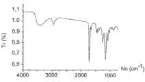
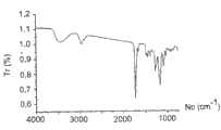
- 238000002129infrared reflectance spectroscopyMethods0.000description8
- 229910021607Silver chlorideInorganic materials0.000description7
- 239000007943implantSubstances0.000description7
- 238000003760magnetic stirringMethods0.000description7
- 239000012044organic layerSubstances0.000description7
- 229920006254polymer filmPolymers0.000description7
- HKZLPVFGJNLROG-UHFFFAOYSA-Msilver monochlorideChemical compound[Cl-].[Ag+]HKZLPVFGJNLROG-UHFFFAOYSA-M0.000description7
- 229910001961silver nitrateInorganic materials0.000description7
- 238000012360testing methodMethods0.000description7
- CSCPPACGZOOCGX-UHFFFAOYSA-NAcetoneChemical compoundCC(C)=OCSCPPACGZOOCGX-UHFFFAOYSA-N0.000description6
- 239000012691Cu precursorSubstances0.000description6
- 238000005229chemical vapour depositionMethods0.000description6
- 229920001940conductive polymerPolymers0.000description6
- 239000012153distilled waterSubstances0.000description6
- 230000007246mechanismEffects0.000description6
- 230000000269nucleophilic effectEffects0.000description6
- 230000010287polarizationEffects0.000description6
- 230000009467reductionEffects0.000description6
- 239000012779reinforcing materialSubstances0.000description6
- 238000005406washingMethods0.000description6
- 230000008901benefitEffects0.000description5
- 239000003054catalystSubstances0.000description5
- 125000004122cyclic groupChemical group0.000description5
- 238000009713electroplatingMethods0.000description5
- 238000011049fillingMethods0.000description5
- 238000007306functionalization reactionMethods0.000description5
- 230000035515penetrationEffects0.000description5
- 239000000377silicon dioxideSubstances0.000description5
- 235000012239silicon dioxideNutrition0.000description5
- 230000009466transformationEffects0.000description5
- YMMGRPLNZPTZBS-UHFFFAOYSA-N2,3-dihydrothieno[2,3-b][1,4]dioxineChemical compoundO1CCOC2=C1C=CS2YMMGRPLNZPTZBS-UHFFFAOYSA-N0.000description4
- PAYRUJLWNCNPSJ-UHFFFAOYSA-NAnilineChemical compoundNC1=CC=CC=C1PAYRUJLWNCNPSJ-UHFFFAOYSA-N0.000description4
- XKRFYHLGVUSROY-UHFFFAOYSA-NArgonChemical compound[Ar]XKRFYHLGVUSROY-UHFFFAOYSA-N0.000description4
- OKTJSMMVPCPJKN-UHFFFAOYSA-NCarbonChemical compound[C]OKTJSMMVPCPJKN-UHFFFAOYSA-N0.000description4
- 108020004414DNAProteins0.000description4
- KAESVJOAVNADME-UHFFFAOYSA-NPyrroleChemical compoundC=1C=CNC=1KAESVJOAVNADME-UHFFFAOYSA-N0.000description4
- YTPLMLYBLZKORZ-UHFFFAOYSA-NThiopheneChemical compoundC=1C=CSC=1YTPLMLYBLZKORZ-UHFFFAOYSA-N0.000description4
- 229910052783alkali metalInorganic materials0.000description4
- 150000001340alkali metalsChemical class0.000description4
- 229910052784alkaline earth metalInorganic materials0.000description4
- 238000013459approachMethods0.000description4
- 238000005260corrosionMethods0.000description4
- 238000002474experimental methodMethods0.000description4
- 230000008595infiltrationEffects0.000description4
- 238000001764infiltrationMethods0.000description4
- 238000002329infrared spectrumMethods0.000description4
- 239000012212insulatorSubstances0.000description4
- 239000011159matrix materialSubstances0.000description4
- 230000005499meniscusEffects0.000description4
- XYJRXVWERLGGKC-UHFFFAOYSA-Dpentacalcium;hydroxide;triphosphateChemical compound[OH-].[Ca+2].[Ca+2].[Ca+2].[Ca+2].[Ca+2].[O-]P([O-])([O-])=O.[O-]P([O-])([O-])=O.[O-]P([O-])([O-])=OXYJRXVWERLGGKC-UHFFFAOYSA-D0.000description4
- 238000005240physical vapour depositionMethods0.000description4
- 238000000623plasma-assisted chemical vapour depositionMethods0.000description4
- 235000018102proteinsNutrition0.000description4
- 108090000623proteins and genesProteins0.000description4
- 102000004169proteins and genesHuman genes0.000description4
- UMJSCPRVCHMLSP-UHFFFAOYSA-NpyridineNatural productsCOC1=CC=CN=C1UMJSCPRVCHMLSP-UHFFFAOYSA-N0.000description4
- 230000003014reinforcing effectEffects0.000description4
- 229920006395saturated elastomerPolymers0.000description4
- 238000004626scanning electron microscopyMethods0.000description4
- 238000004528spin coatingMethods0.000description4
- MYRTYDVEIRVNKP-UHFFFAOYSA-N1,2-DivinylbenzeneChemical compoundC=CC1=CC=CC=C1C=CMYRTYDVEIRVNKP-UHFFFAOYSA-N0.000description3
- UHOVQNZJYSORNB-UHFFFAOYSA-NBenzeneChemical groupC1=CC=CC=C1UHOVQNZJYSORNB-UHFFFAOYSA-N0.000description3
- LYCAIKOWRPUZTN-UHFFFAOYSA-NEthylene glycolChemical compoundOCCOLYCAIKOWRPUZTN-UHFFFAOYSA-N0.000description3
- 239000004372Polyvinyl alcoholSubstances0.000description3
- 125000000217alkyl groupChemical group0.000description3
- 125000003277amino groupChemical group0.000description3
- 125000003178carboxy groupChemical group[H]OC(*)=O0.000description3
- 229910052681coesiteInorganic materials0.000description3
- 230000000295complement effectEffects0.000description3
- 239000002322conducting polymerSubstances0.000description3
- 238000010276constructionMethods0.000description3
- 229910052906cristobaliteInorganic materials0.000description3
- 230000000694effectsEffects0.000description3
- 239000003792electrolyteSubstances0.000description3
- 239000012634fragmentSubstances0.000description3
- 150000004676glycansChemical class0.000description3
- 239000010439graphiteSubstances0.000description3
- 229910002804graphiteInorganic materials0.000description3
- 230000005484gravityEffects0.000description3
- 230000000977initiatory effectEffects0.000description3
- 230000003993interactionEffects0.000description3
- 150000002596lactonesChemical class0.000description3
- CDOSHBSSFJOMGT-UHFFFAOYSA-NlinaloolChemical compoundCC(C)=CCCC(C)(O)C=CCDOSHBSSFJOMGT-UHFFFAOYSA-N0.000description3
- 238000005259measurementMethods0.000description3
- 230000003647oxidationEffects0.000description3
- 238000007254oxidation reactionMethods0.000description3
- 229920000083poly(allylamine)Polymers0.000description3
- 229920000867polyelectrolytePolymers0.000description3
- 238000006116polymerization reactionMethods0.000description3
- 229920001282polysaccharidePolymers0.000description3
- 239000005017polysaccharideSubstances0.000description3
- 229920002451polyvinyl alcoholPolymers0.000description3
- 230000008439repair processEffects0.000description3
- 238000001878scanning electron micrographMethods0.000description3
- 229910052682stishoviteInorganic materials0.000description3
- 229910052905tridymiteInorganic materials0.000description3
- 238000002604ultrasonographyMethods0.000description3
- PAPBSGBWRJIAAV-UHFFFAOYSA-Nε-CaprolactoneChemical compoundO=C1CCCCCO1PAPBSGBWRJIAAV-UHFFFAOYSA-N0.000description3
- 108091032973(ribonucleotides)n+mProteins0.000description2
- YEJRWHAVMIAJKC-UHFFFAOYSA-N4-ButyrolactoneChemical compoundO=C1CCCO1YEJRWHAVMIAJKC-UHFFFAOYSA-N0.000description2
- QGZKDVFQNNGYKY-UHFFFAOYSA-NAmmoniaChemical compoundNQGZKDVFQNNGYKY-UHFFFAOYSA-N0.000description2
- IJGRMHOSHXDMSA-UHFFFAOYSA-NAtomic nitrogenChemical compoundN#NIJGRMHOSHXDMSA-UHFFFAOYSA-N0.000description2
- HEDRZPFGACZZDS-UHFFFAOYSA-NChloroformChemical compoundClC(Cl)ClHEDRZPFGACZZDS-UHFFFAOYSA-N0.000description2
- 102000053602DNAHuman genes0.000description2
- 229920002307DextranPolymers0.000description2
- RTZKZFJDLAIYFH-UHFFFAOYSA-NDiethyl etherChemical compoundCCOCCRTZKZFJDLAIYFH-UHFFFAOYSA-N0.000description2
- KCXVZYZYPLLWCC-UHFFFAOYSA-NEDTAChemical compoundOC(=O)CN(CC(O)=O)CCN(CC(O)=O)CC(O)=OKCXVZYZYPLLWCC-UHFFFAOYSA-N0.000description2
- VEXZGXHMUGYJMC-UHFFFAOYSA-NHydrochloric acidChemical compoundClVEXZGXHMUGYJMC-UHFFFAOYSA-N0.000description2
- 206010061218InflammationDiseases0.000description2
- 108091034117OligonucleotideProteins0.000description2
- 229910019142PO4Inorganic materials0.000description2
- ISWSIDIOOBJBQZ-UHFFFAOYSA-NPhenolChemical compoundOC1=CC=CC=C1ISWSIDIOOBJBQZ-UHFFFAOYSA-N0.000description2
- XYFCBTPGUUZFHI-UHFFFAOYSA-NPhosphineChemical compoundPXYFCBTPGUUZFHI-UHFFFAOYSA-N0.000description2
- 229920002845Poly(methacrylic acid)Polymers0.000description2
- 229920001710PolyorthoesterPolymers0.000description2
- XUIMIQQOPSSXEZ-UHFFFAOYSA-NSiliconChemical compound[Si]XUIMIQQOPSSXEZ-UHFFFAOYSA-N0.000description2
- QAOWNCQODCNURD-UHFFFAOYSA-NSulfuric acidChemical compoundOS(O)(=O)=OQAOWNCQODCNURD-UHFFFAOYSA-N0.000description2
- NRTOMJZYCJJWKI-UHFFFAOYSA-NTitanium nitrideChemical compound[Ti]#NNRTOMJZYCJJWKI-UHFFFAOYSA-N0.000description2
- YXFVVABEGXRONW-UHFFFAOYSA-NTolueneNatural productsCC1=CC=CC=C1YXFVVABEGXRONW-UHFFFAOYSA-N0.000description2
- XSQUKJJJFZCRTK-UHFFFAOYSA-NUreaChemical compoundNC(N)=OXSQUKJJJFZCRTK-UHFFFAOYSA-N0.000description2
- HCHKCACWOHOZIP-UHFFFAOYSA-NZincChemical compound[Zn]HCHKCACWOHOZIP-UHFFFAOYSA-N0.000description2
- JLCPHMBAVCMARE-UHFFFAOYSA-N[3-[[3-[[3-[[3-[[3-[[3-[[3-[[3-[[3-[[3-[[3-[[5-(2-amino-6-oxo-1H-purin-9-yl)-3-[[3-[[3-[[3-[[3-[[3-[[5-(2-amino-6-oxo-1H-purin-9-yl)-3-[[5-(2-amino-6-oxo-1H-purin-9-yl)-3-hydroxyoxolan-2-yl]methoxy-hydroxyphosphoryl]oxyoxolan-2-yl]methoxy-hydroxyphosphoryl]oxy-5-(5-methyl-2,4-dioxopyrimidin-1-yl)oxolan-2-yl]methoxy-hydroxyphosphoryl]oxy-5-(6-aminopurin-9-yl)oxolan-2-yl]methoxy-hydroxyphosphoryl]oxy-5-(6-aminopurin-9-yl)oxolan-2-yl]methoxy-hydroxyphosphoryl]oxy-5-(6-aminopurin-9-yl)oxolan-2-yl]methoxy-hydroxyphosphoryl]oxy-5-(6-aminopurin-9-yl)oxolan-2-yl]methoxy-hydroxyphosphoryl]oxyoxolan-2-yl]methoxy-hydroxyphosphoryl]oxy-5-(5-methyl-2,4-dioxopyrimidin-1-yl)oxolan-2-yl]methoxy-hydroxyphosphoryl]oxy-5-(4-amino-2-oxopyrimidin-1-yl)oxolan-2-yl]methoxy-hydroxyphosphoryl]oxy-5-(5-methyl-2,4-dioxopyrimidin-1-yl)oxolan-2-yl]methoxy-hydroxyphosphoryl]oxy-5-(5-methyl-2,4-dioxopyrimidin-1-yl)oxolan-2-yl]methoxy-hydroxyphosphoryl]oxy-5-(6-aminopurin-9-yl)oxolan-2-yl]methoxy-hydroxyphosphoryl]oxy-5-(6-aminopurin-9-yl)oxolan-2-yl]methoxy-hydroxyphosphoryl]oxy-5-(4-amino-2-oxopyrimidin-1-yl)oxolan-2-yl]methoxy-hydroxyphosphoryl]oxy-5-(4-amino-2-oxopyrimidin-1-yl)oxolan-2-yl]methoxy-hydroxyphosphoryl]oxy-5-(4-amino-2-oxopyrimidin-1-yl)oxolan-2-yl]methoxy-hydroxyphosphoryl]oxy-5-(6-aminopurin-9-yl)oxolan-2-yl]methoxy-hydroxyphosphoryl]oxy-5-(4-amino-2-oxopyrimidin-1-yl)oxolan-2-yl]methyl [5-(6-aminopurin-9-yl)-2-(hydroxymethyl)oxolan-3-yl] hydrogen phosphatePolymersCc1cn(C2CC(OP(O)(=O)OCC3OC(CC3OP(O)(=O)OCC3OC(CC3O)n3cnc4c3nc(N)[nH]c4=O)n3cnc4c3nc(N)[nH]c4=O)C(COP(O)(=O)OC3CC(OC3COP(O)(=O)OC3CC(OC3COP(O)(=O)OC3CC(OC3COP(O)(=O)OC3CC(OC3COP(O)(=O)OC3CC(OC3COP(O)(=O)OC3CC(OC3COP(O)(=O)OC3CC(OC3COP(O)(=O)OC3CC(OC3COP(O)(=O)OC3CC(OC3COP(O)(=O)OC3CC(OC3COP(O)(=O)OC3CC(OC3COP(O)(=O)OC3CC(OC3COP(O)(=O)OC3CC(OC3COP(O)(=O)OC3CC(OC3COP(O)(=O)OC3CC(OC3COP(O)(=O)OC3CC(OC3COP(O)(=O)OC3CC(OC3CO)n3cnc4c(N)ncnc34)n3ccc(N)nc3=O)n3cnc4c(N)ncnc34)n3ccc(N)nc3=O)n3ccc(N)nc3=O)n3ccc(N)nc3=O)n3cnc4c(N)ncnc34)n3cnc4c(N)ncnc34)n3cc(C)c(=O)[nH]c3=O)n3cc(C)c(=O)[nH]c3=O)n3ccc(N)nc3=O)n3cc(C)c(=O)[nH]c3=O)n3cnc4c3nc(N)[nH]c4=O)n3cnc4c(N)ncnc34)n3cnc4c(N)ncnc34)n3cnc4c(N)ncnc34)n3cnc4c(N)ncnc34)O2)c(=O)[nH]c1=OJLCPHMBAVCMARE-UHFFFAOYSA-N0.000description2
- 239000000654additiveSubstances0.000description2
- 230000001464adherent effectEffects0.000description2
- 150000001298alcoholsChemical class0.000description2
- 238000000137annealingMethods0.000description2
- 229940111121antirheumatic drug quinolinesDrugs0.000description2
- 229910052786argonInorganic materials0.000description2
- 150000004982aromatic aminesChemical class0.000description2
- 238000000277atomic layer chemical vapour depositionMethods0.000description2
- 230000006399behaviorEffects0.000description2
- WPYMKLBDIGXBTP-UHFFFAOYSA-Nbenzoic acidChemical compoundOC(=O)C1=CC=CC=C1WPYMKLBDIGXBTP-UHFFFAOYSA-N0.000description2
- 230000001588bifunctional effectEffects0.000description2
- 229910000389calcium phosphateInorganic materials0.000description2
- 150000007942carboxylatesChemical class0.000description2
- 239000000919ceramicSubstances0.000description2
- 238000012512characterization methodMethods0.000description2
- 238000005234chemical depositionMethods0.000description2
- 239000000460chlorineSubstances0.000description2
- 229910052801chlorineInorganic materials0.000description2
- 238000004140cleaningMethods0.000description2
- 239000002131composite materialSubstances0.000description2
- 229920001577copolymerPolymers0.000description2
- 230000007797corrosionEffects0.000description2
- 230000007812deficiencyEffects0.000description2
- 239000004053dental implantSubstances0.000description2
- 238000005137deposition processMethods0.000description2
- 238000010586diagramMethods0.000description2
- 238000006193diazotization reactionMethods0.000description2
- YPTUAQWMBNZZRN-UHFFFAOYSA-NdimethylaminoboronChemical compound[B]N(C)CYPTUAQWMBNZZRN-UHFFFAOYSA-N0.000description2
- 238000003618dip coatingMethods0.000description2
- 230000008034disappearanceEffects0.000description2
- 238000001035dryingMethods0.000description2
- 239000002659electrodepositSubstances0.000description2
- VANNPISTIUFMLH-UHFFFAOYSA-Nglutaric anhydrideChemical compoundO=C1CCCC(=O)O1VANNPISTIUFMLH-UHFFFAOYSA-N0.000description2
- 229920000578graft copolymerPolymers0.000description2
- 229910052588hydroxylapatiteInorganic materials0.000description2
- 230000001976improved effectEffects0.000description2
- 230000004054inflammatory processEffects0.000description2
- 239000003999initiatorSubstances0.000description2
- 239000002648laminated materialSubstances0.000description2
- 239000003446ligandSubstances0.000description2
- 230000014759maintenance of locationEffects0.000description2
- 238000004519manufacturing processMethods0.000description2
- 238000001465metallisationMethods0.000description2
- CERQOIWHTDAKMF-UHFFFAOYSA-Mmethacrylate groupChemical groupC(C(=C)C)(=O)[O-]CERQOIWHTDAKMF-UHFFFAOYSA-M0.000description2
- BDJRBEYXGGNYIS-UHFFFAOYSA-Nnonanedioic acidChemical compoundOC(=O)CCCCCCCC(O)=OBDJRBEYXGGNYIS-UHFFFAOYSA-N0.000description2
- 239000003960organic solventSubstances0.000description2
- 125000002524organometallic groupChemical group0.000description2
- 230000000399orthopedic effectEffects0.000description2
- 235000021317phosphateNutrition0.000description2
- 238000007747platingMethods0.000description2
- 229920003214poly(methacrylonitrile)Polymers0.000description2
- 239000002745poly(ortho ester)Substances0.000description2
- 229920001610polycaprolactonePolymers0.000description2
- 238000002203pretreatmentMethods0.000description2
- 150000003248quinolinesChemical class0.000description2
- 229910052710siliconInorganic materials0.000description2
- 239000010703siliconSubstances0.000description2
- VWDWKYIASSYTQR-UHFFFAOYSA-Nsodium nitrateChemical compound[Na+].[O-][N+]([O-])=OVWDWKYIASSYTQR-UHFFFAOYSA-N0.000description2
- LPXPTNMVRIOKMN-UHFFFAOYSA-Msodium nitriteChemical compound[Na+].[O-]N=OLPXPTNMVRIOKMN-UHFFFAOYSA-M0.000description2
- 238000000527sonicationMethods0.000description2
- 230000002269spontaneous effectEffects0.000description2
- 239000007921spraySubstances0.000description2
- 229930192474thiopheneNatural products0.000description2
- 239000011135tinSubstances0.000description2
- 229910052725zincInorganic materials0.000description2
- 239000011701zincSubstances0.000description2
- NXLNNXIXOYSCMB-UHFFFAOYSA-N(4-nitrophenyl) carbonochloridateChemical group[O-][N+](=O)C1=CC=C(OC(Cl)=O)C=C1NXLNNXIXOYSCMB-UHFFFAOYSA-N0.000description1
- 125000004169(C1-C6) alkyl groupChemical group0.000description1
- NLMDJJTUQPXZFG-UHFFFAOYSA-N1,4,10,13-tetraoxa-7,16-diazacyclooctadecaneChemical compoundC1COCCOCCNCCOCCOCCN1NLMDJJTUQPXZFG-UHFFFAOYSA-N0.000description1
- 1250000000222-aminoethyl groupChemical group[H]C([*])([H])C([H])([H])N([H])[H]0.000description1
- XQQBUAPQHNYYRS-UHFFFAOYSA-N2-methylthiopheneChemical compoundCC1=CC=CS1XQQBUAPQHNYYRS-UHFFFAOYSA-N0.000description1
- KGIGUEBEKRSTEW-UHFFFAOYSA-N2-vinylpyridineChemical compoundC=CC1=CC=CC=N1KGIGUEBEKRSTEW-UHFFFAOYSA-N0.000description1
- NIXOWILDQLNWCW-UHFFFAOYSA-MAcrylateChemical compound[O-]C(=O)C=CNIXOWILDQLNWCW-UHFFFAOYSA-M0.000description1
- NLXLAEXVIDQMFP-UHFFFAOYSA-NAmmonium chlorideSubstances[NH4+].[Cl-]NLXLAEXVIDQMFP-UHFFFAOYSA-N0.000description1
- VHUUQVKOLVNVRT-UHFFFAOYSA-NAmmonium hydroxideChemical compound[NH4+].[OH-]VHUUQVKOLVNVRT-UHFFFAOYSA-N0.000description1
- 239000005711Benzoic acidSubstances0.000description1
- OYPRJOBELJOOCE-UHFFFAOYSA-NCalciumChemical compound[Ca]OYPRJOBELJOOCE-UHFFFAOYSA-N0.000description1
- BVKZGUZCCUSVTD-UHFFFAOYSA-LCarbonateChemical compound[O-]C([O-])=OBVKZGUZCCUSVTD-UHFFFAOYSA-L0.000description1
- 229920001661ChitosanPolymers0.000description1
- ZAMOUSCENKQFHK-UHFFFAOYSA-NChlorine atomChemical compound[Cl]ZAMOUSCENKQFHK-UHFFFAOYSA-N0.000description1
- 239000004971Cross linkerSubstances0.000description1
- 229920000858CyclodextrinPolymers0.000description1
- 102100028630Cytoskeleton-associated protein 2Human genes0.000description1
- BWGNESOTFCXPMA-UHFFFAOYSA-NDihydrogen disulfideChemical compoundSSBWGNESOTFCXPMA-UHFFFAOYSA-N0.000description1
- BRLQWZUYTZBJKN-UHFFFAOYSA-NEpichlorohydrinChemical compoundClCC1CO1BRLQWZUYTZBJKN-UHFFFAOYSA-N0.000description1
- 239000004593EpoxySubstances0.000description1
- IAYPIBMASNFSPL-UHFFFAOYSA-NEthylene oxideChemical compoundC1CO1IAYPIBMASNFSPL-UHFFFAOYSA-N0.000description1
- PIICEJLVQHRZGT-UHFFFAOYSA-NEthylenediamineChemical compoundNCCNPIICEJLVQHRZGT-UHFFFAOYSA-N0.000description1
- 102000009123FibrinHuman genes0.000description1
- 108010073385FibrinProteins0.000description1
- BWGVNKXGVNDBDI-UHFFFAOYSA-NFibrin monomerChemical compoundCNC(=O)CNC(=O)CNBWGVNKXGVNDBDI-UHFFFAOYSA-N0.000description1
- WQZGKKKJIJFFOK-GASJEMHNSA-NGlucoseNatural productsOC[C@H]1OC(O)[C@H](O)[C@@H](O)[C@@H]1OWQZGKKKJIJFFOK-GASJEMHNSA-N0.000description1
- SXRSQZLOMIGNAQ-UHFFFAOYSA-NGlutaraldehydeChemical compoundO=CCCCC=OSXRSQZLOMIGNAQ-UHFFFAOYSA-N0.000description1
- HTTJABKRGRZYRN-UHFFFAOYSA-NHeparinChemical compoundOC1C(NC(=O)C)C(O)OC(COS(O)(=O)=O)C1OC1C(OS(O)(=O)=O)C(O)C(OC2C(C(OS(O)(=O)=O)C(OC3C(C(O)C(O)C(O3)C(O)=O)OS(O)(=O)=O)C(CO)O2)NS(O)(=O)=O)C(C(O)=O)O1HTTJABKRGRZYRN-UHFFFAOYSA-N0.000description1
- 101000766848Homo sapiens Cytoskeleton-associated protein 2Proteins0.000description1
- UFHFLCQGNIYNRP-UHFFFAOYSA-NHydrogenChemical compound[H][H]UFHFLCQGNIYNRP-UHFFFAOYSA-N0.000description1
- 239000002879Lewis baseSubstances0.000description1
- OFOBLEOULBTSOW-UHFFFAOYSA-NMalonic acidChemical compoundOC(=O)CC(O)=OOFOBLEOULBTSOW-UHFFFAOYSA-N0.000description1
- QENGPZGAWFQWCZ-UHFFFAOYSA-NMethylthiopheneNatural productsCC=1C=CSC=1QENGPZGAWFQWCZ-UHFFFAOYSA-N0.000description1
- MSFSPUZXLOGKHJ-UHFFFAOYSA-NMuraminsaeureNatural productsOC(=O)C(C)OC1C(N)C(O)OC(CO)C1OMSFSPUZXLOGKHJ-UHFFFAOYSA-N0.000description1
- 101100189356Mus musculus Papolb geneProteins0.000description1
- VEQPNABPJHWNSG-UHFFFAOYSA-NNickel(2+)Chemical compound[Ni+2]VEQPNABPJHWNSG-UHFFFAOYSA-N0.000description1
- 229910021586Nickel(II) chlorideInorganic materials0.000description1
- XOJVVFBFDXDTEG-UHFFFAOYSA-NNorphytaneNatural productsCC(C)CCCC(C)CCCC(C)CCCC(C)CXOJVVFBFDXDTEG-UHFFFAOYSA-N0.000description1
- 108010013639PeptidoglycanProteins0.000description1
- 239000004952PolyamideSubstances0.000description1
- 239000004698PolyethyleneSubstances0.000description1
- 229920002873PolyethyleniminePolymers0.000description1
- 239000000589SiderophoreSubstances0.000description1
- 108020004682Single-Stranded DNAProteins0.000description1
- 229920002125Sokalan®Polymers0.000description1
- 229910000831SteelInorganic materials0.000description1
- QAOWNCQODCNURD-UHFFFAOYSA-LSulfateChemical compound[O-]S([O-])(=O)=OQAOWNCQODCNURD-UHFFFAOYSA-L0.000description1
- NINIDFKCEFEMDL-UHFFFAOYSA-NSulfurChemical group[S]NINIDFKCEFEMDL-UHFFFAOYSA-N0.000description1
- 238000000026X-ray photoelectron spectrumMethods0.000description1
- 238000002679ablationMethods0.000description1
- 150000008065acid anhydridesChemical class0.000description1
- 150000003926acrylamidesChemical class0.000description1
- 150000001255actinidesChemical class0.000description1
- 150000004996alkyl benzenesChemical class0.000description1
- 125000005600alkyl phosphonate groupChemical group0.000description1
- 229910045601alloyInorganic materials0.000description1
- 239000000956alloySubstances0.000description1
- 235000001014amino acidNutrition0.000description1
- 150000001413amino acidsChemical class0.000description1
- 229910021529ammoniaInorganic materials0.000description1
- 235000011114ammonium hydroxideNutrition0.000description1
- 238000004458analytical methodMethods0.000description1
- 238000002048anodisation reactionMethods0.000description1
- 239000003242anti bacterial agentSubstances0.000description1
- 229940088710antibiotic agentDrugs0.000description1
- 229910052586apatiteInorganic materials0.000description1
- 230000001174ascending effectEffects0.000description1
- 150000001555benzenesChemical group0.000description1
- 235000010233benzoic acidNutrition0.000description1
- 229910001423beryllium ionInorganic materials0.000description1
- 229920000249biocompatible polymerPolymers0.000description1
- 230000005540biological transmissionEffects0.000description1
- 230000003592biomimetic effectEffects0.000description1
- 210000002449bone cellAnatomy0.000description1
- KGBXLFKZBHKPEV-UHFFFAOYSA-Nboric acidChemical compoundOB(O)OKGBXLFKZBHKPEV-UHFFFAOYSA-N0.000description1
- 239000004327boric acidSubstances0.000description1
- ODWXUNBKCRECNW-UHFFFAOYSA-Mbromocopper(1+)Chemical compoundBr[Cu+]ODWXUNBKCRECNW-UHFFFAOYSA-M0.000description1
- 125000000484butyl groupChemical group[H]C([*])([H])C([H])([H])C([H])([H])C([H])([H])[H]0.000description1
- 229930188620butyrolactoneNatural products0.000description1
- 239000011575calciumSubstances0.000description1
- 239000001506calcium phosphateSubstances0.000description1
- 235000011010calcium phosphatesNutrition0.000description1
- VTJUKNSKBAOEHE-UHFFFAOYSA-NcalixareneChemical compoundCOC(=O)COC1=C(CC=2C(=C(CC=3C(=C(C4)C=C(C=3)C(C)(C)C)OCC(=O)OC)C=C(C=2)C(C)(C)C)OCC(=O)OC)C=C(C(C)(C)C)C=C1CC1=C(OCC(=O)OC)C4=CC(C(C)(C)C)=C1VTJUKNSKBAOEHE-UHFFFAOYSA-N0.000description1
- 239000004202carbamideSubstances0.000description1
- 229910052799carbonInorganic materials0.000description1
- 125000002915carbonyl groupChemical group[*:2]C([*:1])=O0.000description1
- 125000002843carboxylic acid groupChemical group0.000description1
- 150000001735carboxylic acidsChemical class0.000description1
- 239000000969carrierSubstances0.000description1
- 239000012159carrier gasSubstances0.000description1
- 239000005018caseinSubstances0.000description1
- BECPQYXYKAMYBN-UHFFFAOYSA-Ncasein, tech.Chemical compoundNCCCCC(C(O)=O)N=C(O)C(CC(O)=O)N=C(O)C(CCC(O)=N)N=C(O)C(CC(C)C)N=C(O)C(CCC(O)=O)N=C(O)C(CC(O)=O)N=C(O)C(CCC(O)=O)N=C(O)C(C(C)O)N=C(O)C(CCC(O)=N)N=C(O)C(CCC(O)=N)N=C(O)C(CCC(O)=N)N=C(O)C(CCC(O)=O)N=C(O)C(CCC(O)=O)N=C(O)C(COP(O)(O)=O)N=C(O)C(CCC(O)=N)N=C(O)C(N)CC1=CC=CC=C1BECPQYXYKAMYBN-UHFFFAOYSA-N0.000description1
- 235000021240caseinsNutrition0.000description1
- 238000006555catalytic reactionMethods0.000description1
- 210000004027cellAnatomy0.000description1
- 239000001913celluloseSubstances0.000description1
- 229920002678cellulosePolymers0.000description1
- 239000003153chemical reaction reagentSubstances0.000description1
- 239000003638chemical reducing agentSubstances0.000description1
- 150000001805chlorine compoundsChemical class0.000description1
- 238000000975co-precipitationMethods0.000description1
- 238000010668complexation reactionMethods0.000description1
- 239000008139complexing agentSubstances0.000description1
- 238000009833condensationMethods0.000description1
- 230000005494condensationEffects0.000description1
- 238000012790confirmationMethods0.000description1
- 150000001879copperChemical class0.000description1
- 230000008878couplingEffects0.000description1
- 238000010168coupling processMethods0.000description1
- 238000005859coupling reactionMethods0.000description1
- 239000003431cross linking reagentSubstances0.000description1
- 150000003983crown ethersChemical class0.000description1
- 239000002739cryptandSubstances0.000description1
- 239000013078crystalSubstances0.000description1
- ZXTYDZYHMVIHLP-UHFFFAOYSA-Ncyano 2-methylprop-2-enoateChemical classCC(=C)C(=O)OC#NZXTYDZYHMVIHLP-UHFFFAOYSA-N0.000description1
- NLCKLZIHJQEMCU-UHFFFAOYSA-Ncyano prop-2-enoateChemical classC=CC(=O)OC#NNLCKLZIHJQEMCU-UHFFFAOYSA-N0.000description1
- 229940097362cyclodextrinsDrugs0.000description1
- 125000000151cysteine groupChemical groupN[C@@H](CS)C(=O)*0.000description1
- 230000007547defectEffects0.000description1
- 230000001419dependent effectEffects0.000description1
- 125000004386diacrylate groupChemical group0.000description1
- IJGRMHOSHXDMSA-UHFFFAOYSA-OdiazyniumChemical compound[NH+]#NIJGRMHOSHXDMSA-UHFFFAOYSA-O0.000description1
- 235000014113dietary fatty acidsNutrition0.000description1
- WOERBKLLTSWFBY-UHFFFAOYSA-Mdihydrogen phosphate;tetramethylazaniumChemical compoundC[N+](C)(C)C.OP(O)([O-])=OWOERBKLLTSWFBY-UHFFFAOYSA-M0.000description1
- MHJAJDCZWVHCPF-UHFFFAOYSA-Ldimagnesium phosphateChemical compound[Mg+2].OP([O-])([O-])=OMHJAJDCZWVHCPF-UHFFFAOYSA-L0.000description1
- 229910000395dimagnesium phosphateInorganic materials0.000description1
- 230000009977dual effectEffects0.000description1
- 238000003487electrochemical reactionMethods0.000description1
- 238000000157electrochemical-induced impedance spectroscopyMethods0.000description1
- 238000001962electrophoresisMethods0.000description1
- 230000009881electrostatic interactionEffects0.000description1
- 238000005538encapsulationMethods0.000description1
- 239000003623enhancerSubstances0.000description1
- 230000002708enhancing effectEffects0.000description1
- 125000003700epoxy groupChemical group0.000description1
- CEIPQQODRKXDSB-UHFFFAOYSA-Nethyl 3-(6-hydroxynaphthalen-2-yl)-1H-indazole-5-carboximidate dihydrochlorideChemical compoundCl.Cl.C1=C(O)C=CC2=CC(C3=NNC4=CC=C(C=C43)C(=N)OCC)=CC=C21CEIPQQODRKXDSB-UHFFFAOYSA-N0.000description1
- 125000004494ethyl ester groupChemical group0.000description1
- 150000002171ethylene diaminesChemical class0.000description1
- 229940093476ethylene glycolDrugs0.000description1
- 229940071106ethylenediaminetetraacetateDrugs0.000description1
- 238000011156evaluationMethods0.000description1
- 230000005284excitationEffects0.000description1
- 210000003722extracellular fluidAnatomy0.000description1
- 238000000605extractionMethods0.000description1
- 239000000194fatty acidSubstances0.000description1
- 229930195729fatty acidNatural products0.000description1
- 230000002349favourable effectEffects0.000description1
- YAGKRVSRTSUGEY-UHFFFAOYSA-NferricyanideChemical compound[Fe+3].N#[C-].N#[C-].N#[C-].N#[C-].N#[C-].N#[C-]YAGKRVSRTSUGEY-UHFFFAOYSA-N0.000description1
- 229950003499fibrinDrugs0.000description1
- 239000012530fluidSubstances0.000description1
- 238000011010flushing procedureMethods0.000description1
- 239000008103glucoseSubstances0.000description1
- 229920000669heparinPolymers0.000description1
- 229960002897heparinDrugs0.000description1
- 238000001198high resolution scanning electron microscopyMethods0.000description1
- 239000012943hotmeltSubstances0.000description1
- ARRNBPCNZJXHRJ-UHFFFAOYSA-Mhydron;tetrabutylazanium;phosphateChemical compoundOP(O)([O-])=O.CCCC[N+](CCCC)(CCCC)CCCCARRNBPCNZJXHRJ-UHFFFAOYSA-M0.000description1
- 229920001600hydrophobic polymerPolymers0.000description1
- 238000011065in-situ storageMethods0.000description1
- 238000002347injectionMethods0.000description1
- 239000007924injectionSubstances0.000description1
- 238000009413insulationMethods0.000description1
- 238000010884ion-beam techniqueMethods0.000description1
- 150000002527isonitrilesChemical class0.000description1
- 239000007791liquid phaseSubstances0.000description1
- MHCFAGZWMAWTNR-UHFFFAOYSA-Mlithium perchlorateChemical compound[Li+].[O-]Cl(=O)(=O)=OMHCFAGZWMAWTNR-UHFFFAOYSA-M0.000description1
- 229910001486lithium perchlorateInorganic materials0.000description1
- 238000005461lubricationMethods0.000description1
- 229910001510metal chlorideInorganic materials0.000description1
- 239000007769metal materialSubstances0.000description1
- 239000011859microparticleSubstances0.000description1
- 238000002156mixingMethods0.000description1
- 125000000896monocarboxylic acid groupChemical group0.000description1
- 150000002772monosaccharidesChemical class0.000description1
- 230000000877morphologic effectEffects0.000description1
- FYCBGURDLIKBDA-UHFFFAOYSA-Nn-hexyl-2-methylprop-2-enamideChemical classCCCCCCNC(=O)C(C)=CFYCBGURDLIKBDA-UHFFFAOYSA-N0.000description1
- 239000002105nanoparticleSubstances0.000description1
- QMMRZOWCJAIUJA-UHFFFAOYSA-Lnickel dichlorideChemical compoundCl[Ni]ClQMMRZOWCJAIUJA-UHFFFAOYSA-L0.000description1
- LGQLOGILCSXPEA-UHFFFAOYSA-Lnickel sulfateChemical compound[Ni+2].[O-]S([O-])(=O)=OLGQLOGILCSXPEA-UHFFFAOYSA-L0.000description1
- 229910000363nickel(II) sulfateInorganic materials0.000description1
- GTTYPHLDORACJW-UHFFFAOYSA-Nnitric acid;sodiumChemical compound[Na].O[N+]([O-])=OGTTYPHLDORACJW-UHFFFAOYSA-N0.000description1
- 125000002560nitrile groupChemical group0.000description1
- 125000000449nitro groupChemical group[O-][N+](*)=O0.000description1
- 229910052757nitrogenInorganic materials0.000description1
- 229910000510noble metalInorganic materials0.000description1
- 239000012454non-polar solventSubstances0.000description1
- 230000003287optical effectEffects0.000description1
- 150000002894organic compoundsChemical class0.000description1
- 239000012074organic phaseSubstances0.000description1
- 229920000620organic polymerPolymers0.000description1
- 210000000963osteoblastAnatomy0.000description1
- 210000002997osteoclastAnatomy0.000description1
- RECVMTHOQWMYFX-UHFFFAOYSA-Noxygen(1+) dihydrideChemical compound[OH2+]RECVMTHOQWMYFX-UHFFFAOYSA-N0.000description1
- 150000002940palladiumChemical class0.000description1
- WXHIJDCHNDBCNY-UHFFFAOYSA-Npalladium dihydrideChemical compound[PdH2]WXHIJDCHNDBCNY-UHFFFAOYSA-N0.000description1
- 230000003071parasitic effectEffects0.000description1
- VSIIXMUUUJUKCM-UHFFFAOYSA-Dpentacalcium;fluoride;triphosphateChemical compound[F-].[Ca+2].[Ca+2].[Ca+2].[Ca+2].[Ca+2].[O-]P([O-])([O-])=O.[O-]P([O-])([O-])=O.[O-]P([O-])([O-])=OVSIIXMUUUJUKCM-UHFFFAOYSA-D0.000description1
- 125000001147pentyl groupChemical groupC(CCCC)*0.000description1
- VLTRZXGMWDSKGL-UHFFFAOYSA-MperchlorateInorganic materials[O-]Cl(=O)(=O)=OVLTRZXGMWDSKGL-UHFFFAOYSA-M0.000description1
- VLTRZXGMWDSKGL-UHFFFAOYSA-Nperchloric acidChemical compoundOCl(=O)(=O)=OVLTRZXGMWDSKGL-UHFFFAOYSA-N0.000description1
- 125000005385peroxodisulfate groupChemical group0.000description1
- 150000004965peroxy acidsChemical class0.000description1
- JRKICGRDRMAZLK-UHFFFAOYSA-Lpersulfate groupChemical groupS(=O)(=O)([O-])OOS(=O)(=O)[O-]JRKICGRDRMAZLK-UHFFFAOYSA-L0.000description1
- 239000012071phaseSubstances0.000description1
- 239000003444phase transfer catalystSubstances0.000description1
- 150000005041phenanthrolinesChemical class0.000description1
- 150000002989phenolsChemical class0.000description1
- NBIIXXVUZAFLBC-UHFFFAOYSA-KphosphateChemical compound[O-]P([O-])([O-])=ONBIIXXVUZAFLBC-UHFFFAOYSA-K0.000description1
- 239000010452phosphateSubstances0.000description1
- 229910000073phosphorus hydrideInorganic materials0.000description1
- 238000001420photoelectron spectroscopyMethods0.000description1
- 150000003057platinumChemical class0.000description1
- 229920000747poly(lactic acid)Polymers0.000description1
- 229920001606poly(lactic acid-co-glycolic acid)Polymers0.000description1
- 239000004584polyacrylic acidSubstances0.000description1
- 229920002647polyamidePolymers0.000description1
- 229920000647polyepoxidePolymers0.000description1
- 229920000573polyethylenePolymers0.000description1
- 239000004626polylactic acidSubstances0.000description1
- 229920000128polypyrrolePolymers0.000description1
- 150000004032porphyrinsChemical class0.000description1
- 239000000843powderSubstances0.000description1
- 230000001376precipitating effectEffects0.000description1
- 125000002924primary amino groupChemical group[H]N([H])*0.000description1
- 108090000765processed proteins & peptidesProteins0.000description1
- 102000004196processed proteins & peptidesHuman genes0.000description1
- 238000001314profilometryMethods0.000description1
- 230000001737promoting effectEffects0.000description1
- NHARPDSAXCBDDR-UHFFFAOYSA-Npropyl 2-methylprop-2-enoateChemical compoundCCCOC(=O)C(C)=CNHARPDSAXCBDDR-UHFFFAOYSA-N0.000description1
- 125000001436propyl groupChemical group[H]C([*])([H])C([H])([H])C([H])([H])[H]0.000description1
- JUJWROOIHBZHMG-UHFFFAOYSA-OpyridiniumChemical compoundC1=CC=[NH+]C=C1JUJWROOIHBZHMG-UHFFFAOYSA-O0.000description1
- 125000004076pyridyl groupChemical group0.000description1
- 238000010526radical polymerization reactionMethods0.000description1
- 230000001172regenerating effectEffects0.000description1
- 238000011160researchMethods0.000description1
- 230000035945sensitivityEffects0.000description1
- 238000000926separation methodMethods0.000description1
- 239000012890simulated body fluidSubstances0.000description1
- 238000005245sinteringMethods0.000description1
- 239000000344soapSubstances0.000description1
- 239000004317sodium nitrateSubstances0.000description1
- 235000010344sodium nitrateNutrition0.000description1
- 235000010288sodium nitriteNutrition0.000description1
- 239000002689soilSubstances0.000description1
- 238000002798spectrophotometry methodMethods0.000description1
- 238000009987spinningMethods0.000description1
- 239000007858starting materialSubstances0.000description1
- 239000010959steelSubstances0.000description1
- 238000003756stirringMethods0.000description1
- 125000000446sulfanediyl groupChemical group*S*0.000description1
- 150000003871sulfonatesChemical class0.000description1
- 239000011593sulfurSubstances0.000description1
- 229910052717sulfurInorganic materials0.000description1
- DHCDFWKWKRSZHF-UHFFFAOYSA-Nsulfurothioic S-acidChemical classOS(O)(=O)=SDHCDFWKWKRSZHF-UHFFFAOYSA-N0.000description1
- 230000008093supporting effectEffects0.000description1
- 239000003115supporting electrolyteSubstances0.000description1
- 238000005211surface analysisMethods0.000description1
- 238000006557surface reactionMethods0.000description1
- 239000004094surface-active agentSubstances0.000description1
- 238000003786synthesis reactionMethods0.000description1
- 230000009885systemic effectEffects0.000description1
- MZLGASXMSKOWSE-UHFFFAOYSA-Ntantalum nitrideChemical compound[Ta]#NMZLGASXMSKOWSE-UHFFFAOYSA-N0.000description1
- KBLZDCFTQSIIOH-UHFFFAOYSA-Mtetrabutylazanium;perchlorateChemical compound[O-]Cl(=O)(=O)=O.CCCC[N+](CCCC)(CCCC)CCCCKBLZDCFTQSIIOH-UHFFFAOYSA-M0.000description1
- CBXCPBUEXACCNR-UHFFFAOYSA-NtetraethylammoniumChemical compoundCC[N+](CC)(CC)CCCBXCPBUEXACCNR-UHFFFAOYSA-N0.000description1
- QEMXHQIAXOOASZ-UHFFFAOYSA-NtetramethylammoniumChemical compoundC[N+](C)(C)CQEMXHQIAXOOASZ-UHFFFAOYSA-N0.000description1
- OSBSFAARYOCBHB-UHFFFAOYSA-NtetrapropylammoniumChemical compoundCCC[N+](CCC)(CCC)CCCOSBSFAARYOCBHB-UHFFFAOYSA-N0.000description1
- 238000009210therapy by ultrasoundMethods0.000description1
- 150000007944thiolatesChemical class0.000description1
- 150000003585thioureasChemical class0.000description1
- 210000001519tissueAnatomy0.000description1
- 125000003944tolyl groupChemical group0.000description1
- 230000007704transitionEffects0.000description1
- 229910052723transition metalInorganic materials0.000description1
- 150000003624transition metalsChemical class0.000description1
- QORWJWZARLRLPR-UHFFFAOYSA-Htricalcium bis(phosphate)Chemical group[Ca+2].[Ca+2].[Ca+2].[O-]P([O-])([O-])=O.[O-]P([O-])([O-])=OQORWJWZARLRLPR-UHFFFAOYSA-H0.000description1
- 238000002525ultrasonicationMethods0.000description1
- GPPXJZIENCGNKB-UHFFFAOYSA-NvanadiumChemical compound[V]#[V]GPPXJZIENCGNKB-UHFFFAOYSA-N0.000description1
- 230000002792vascularEffects0.000description1
- 238000004832voltammetryMethods0.000description1
- 238000001075voltammogramMethods0.000description1
- 239000002699waste materialSubstances0.000description1
Images


Classifications
- C—CHEMISTRY; METALLURGY
- C23—COATING METALLIC MATERIAL; COATING MATERIAL WITH METALLIC MATERIAL; CHEMICAL SURFACE TREATMENT; DIFFUSION TREATMENT OF METALLIC MATERIAL; COATING BY VACUUM EVAPORATION, BY SPUTTERING, BY ION IMPLANTATION OR BY CHEMICAL VAPOUR DEPOSITION, IN GENERAL; INHIBITING CORROSION OF METALLIC MATERIAL OR INCRUSTATION IN GENERAL
- C23C—COATING METALLIC MATERIAL; COATING MATERIAL WITH METALLIC MATERIAL; SURFACE TREATMENT OF METALLIC MATERIAL BY DIFFUSION INTO THE SURFACE, BY CHEMICAL CONVERSION OR SUBSTITUTION; COATING BY VACUUM EVAPORATION, BY SPUTTERING, BY ION IMPLANTATION OR BY CHEMICAL VAPOUR DEPOSITION, IN GENERAL
- C23C14/00—Coating by vacuum evaporation, by sputtering or by ion implantation of the coating forming material
- C23C14/02—Pretreatment of the material to be coated
- C—CHEMISTRY; METALLURGY
- C25—ELECTROLYTIC OR ELECTROPHORETIC PROCESSES; APPARATUS THEREFOR
- C25D—PROCESSES FOR THE ELECTROLYTIC OR ELECTROPHORETIC PRODUCTION OF COATINGS; ELECTROFORMING; APPARATUS THEREFOR
- C25D15/00—Electrolytic or electrophoretic production of coatings containing embedded materials, e.g. particles, whiskers, wires
- B—PERFORMING OPERATIONS; TRANSPORTING
- B05—SPRAYING OR ATOMISING IN GENERAL; APPLYING FLUENT MATERIALS TO SURFACES, IN GENERAL
- B05D—PROCESSES FOR APPLYING FLUENT MATERIALS TO SURFACES, IN GENERAL
- B05D7/00—Processes, other than flocking, specially adapted for applying liquids or other fluent materials to particular surfaces or for applying particular liquids or other fluent materials
- C—CHEMISTRY; METALLURGY
- C09—DYES; PAINTS; POLISHES; NATURAL RESINS; ADHESIVES; COMPOSITIONS NOT OTHERWISE PROVIDED FOR; APPLICATIONS OF MATERIALS NOT OTHERWISE PROVIDED FOR
- C09D—COATING COMPOSITIONS, e.g. PAINTS, VARNISHES OR LACQUERS; FILLING PASTES; CHEMICAL PAINT OR INK REMOVERS; INKS; CORRECTING FLUIDS; WOODSTAINS; PASTES OR SOLIDS FOR COLOURING OR PRINTING; USE OF MATERIALS THEREFOR
- C09D5/00—Coating compositions, e.g. paints, varnishes or lacquers, characterised by their physical nature or the effects produced; Filling pastes
- C09D5/44—Coating compositions, e.g. paints, varnishes or lacquers, characterised by their physical nature or the effects produced; Filling pastes for electrophoretic applications
- C09D5/4407—Coating compositions, e.g. paints, varnishes or lacquers, characterised by their physical nature or the effects produced; Filling pastes for electrophoretic applications with polymers obtained by polymerisation reactions involving only carbon-to-carbon unsaturated bonds
- C—CHEMISTRY; METALLURGY
- C23—COATING METALLIC MATERIAL; COATING MATERIAL WITH METALLIC MATERIAL; CHEMICAL SURFACE TREATMENT; DIFFUSION TREATMENT OF METALLIC MATERIAL; COATING BY VACUUM EVAPORATION, BY SPUTTERING, BY ION IMPLANTATION OR BY CHEMICAL VAPOUR DEPOSITION, IN GENERAL; INHIBITING CORROSION OF METALLIC MATERIAL OR INCRUSTATION IN GENERAL
- C23C—COATING METALLIC MATERIAL; COATING MATERIAL WITH METALLIC MATERIAL; SURFACE TREATMENT OF METALLIC MATERIAL BY DIFFUSION INTO THE SURFACE, BY CHEMICAL CONVERSION OR SUBSTITUTION; COATING BY VACUUM EVAPORATION, BY SPUTTERING, BY ION IMPLANTATION OR BY CHEMICAL VAPOUR DEPOSITION, IN GENERAL
- C23C26/00—Coating not provided for in groups C23C2/00 - C23C24/00
- C—CHEMISTRY; METALLURGY
- C25—ELECTROLYTIC OR ELECTROPHORETIC PROCESSES; APPARATUS THEREFOR
- C25D—PROCESSES FOR THE ELECTROLYTIC OR ELECTROPHORETIC PRODUCTION OF COATINGS; ELECTROFORMING; APPARATUS THEREFOR
- C25D5/00—Electroplating characterised by the process; Pretreatment or after-treatment of workpieces
- C25D5/34—Pretreatment of metallic surfaces to be electroplated
- C—CHEMISTRY; METALLURGY
- C25—ELECTROLYTIC OR ELECTROPHORETIC PROCESSES; APPARATUS THEREFOR
- C25D—PROCESSES FOR THE ELECTROLYTIC OR ELECTROPHORETIC PRODUCTION OF COATINGS; ELECTROFORMING; APPARATUS THEREFOR
- C25D5/00—Electroplating characterised by the process; Pretreatment or after-treatment of workpieces
- C25D5/54—Electroplating of non-metallic surfaces
- C25D5/56—Electroplating of non-metallic surfaces of plastics
- C—CHEMISTRY; METALLURGY
- C25—ELECTROLYTIC OR ELECTROPHORETIC PROCESSES; APPARATUS THEREFOR
- C25D—PROCESSES FOR THE ELECTROLYTIC OR ELECTROPHORETIC PRODUCTION OF COATINGS; ELECTROFORMING; APPARATUS THEREFOR
- C25D3/00—Electroplating: Baths therefor
- C25D3/02—Electroplating: Baths therefor from solutions
- C25D3/38—Electroplating: Baths therefor from solutions of copper
- Y—GENERAL TAGGING OF NEW TECHNOLOGICAL DEVELOPMENTS; GENERAL TAGGING OF CROSS-SECTIONAL TECHNOLOGIES SPANNING OVER SEVERAL SECTIONS OF THE IPC; TECHNICAL SUBJECTS COVERED BY FORMER USPC CROSS-REFERENCE ART COLLECTIONS [XRACs] AND DIGESTS
- Y10—TECHNICAL SUBJECTS COVERED BY FORMER USPC
- Y10T—TECHNICAL SUBJECTS COVERED BY FORMER US CLASSIFICATION
- Y10T428/00—Stock material or miscellaneous articles
- Y10T428/12—All metal or with adjacent metals
- Y10T428/12493—Composite; i.e., plural, adjacent, spatially distinct metal components [e.g., layers, joint, etc.]
Landscapes
- Chemical & Material Sciences (AREA)
- Engineering & Computer Science (AREA)
- Chemical Kinetics & Catalysis (AREA)
- Materials Engineering (AREA)
- Organic Chemistry (AREA)
- Metallurgy (AREA)
- Electrochemistry (AREA)
- Life Sciences & Earth Sciences (AREA)
- Wood Science & Technology (AREA)
- Mechanical Engineering (AREA)
- Molecular Biology (AREA)
- Health & Medical Sciences (AREA)
- Chemically Coating (AREA)
- Application Of Or Painting With Fluid Materials (AREA)
- Electroplating Methods And Accessories (AREA)
- Other Surface Treatments For Metallic Materials (AREA)
- Electrodes Of Semiconductors (AREA)
- Transition And Organic Metals Composition Catalysts For Addition Polymerization (AREA)
- Glass Compositions (AREA)
- Laminated Bodies (AREA)
Abstract
Translated fromChinese
Description
Translated fromChinese技术领域technical field
本发明涉及将材料沉积或附着在表面上的方法。The present invention relates to methods of depositing or attaching materials to surfaces.
本发明尤其涉及涂布表面的方法,特别是将材料非常粘性地沉积在表面上的方法。In particular, the invention relates to methods of coating surfaces, especially methods of depositing materials on surfaces very viscously.
本发明方法的目的是将任意类型的材料粘性沉积在任意类型的表面上。The purpose of the method of the invention is to adhesively deposit any type of material on any type of surface.
背景技术Background technique
关于常规的表面涂布,以及特别是关于将材料附着于导电或半导体表面上,迄今已描述了许多工艺。为了证实本发明的许多优点,本文下面将依次讨论聚合物在导电或半导体表面上的粘性沉积、金属在导电或半导体表面上的粘性沉积、以及离子绝缘体在导电或半导体表面上的粘性沉积。With regard to conventional surface coating, and particularly with regard to the attachment of materials to conductive or semiconducting surfaces, many processes have been described so far. To demonstrate the many advantages of the present invention, the adhesive deposition of polymers on conductive or semiconducting surfaces, the adhesive deposition of metals on conductive or semiconducting surfaces, and the adhesive deposition of ionic insulators on conductive or semiconducting surfaces are discussed in turn herein below.
通过将目标分子如具有特定性能的分子,附着于表面上并在表面上保留所有或一部分其性能的操作称为官能化。对表面的官能化假设可以利用待附着的目标分子和可以实现将所述分子附着于该表面上的适宜方法。由于目标分子通常是有机或有机金属分子,因此常用的方法在于通过试图发现分别在表面和目标分子上相容的官能团,即可以容易地,并且如果可能的话快速地一起反应,实现大量的有机化学反应库。The operation of attaching target molecules, such as molecules with specific properties, to a surface and retaining all or a part of their properties on the surface is called functionalization. Functionalization of a surface assumes that the target molecule to be attached can be utilized and a suitable method of attaching said molecule to the surface can be achieved. Since the target molecule is usually an organic or organometallic molecule, a common approach consists in realizing a large amount of organic chemistry by trying to find functional groups that are compatible on the surface and on the target molecule, respectively, that can react easily and if possible rapidly together. React library.
例如,当可以利用含有羟基-OH或氨基-NH的表面时,它可以通过给予目标分子如异氰酸酯、硅氧烷、酰基氯等使其官能化。当目标分子不包括直接与表面的这些基团相容的任意官能团时,该表面可以用双官能团中间体有机分子预官能化,其中一个官能团是可以与表面的这些基团相容的官能团,另一个官能团是可以与所需附着的分子的基团相容的官能团。中间体分子有时也被称为粘合引物(adhesiveprimer),如文献[1]中所述。For example, when a surface containing hydroxyl-OH or amino-NH is available, it can be functionalized by imparting target molecules such as isocyanates, siloxanes, acid chlorides, etc. When the target molecule does not include any functional groups that are directly compatible with these groups of the surface, the surface can be prefunctionalized with bifunctional intermediate organic molecules, one of which is a functional group that is compatible with these groups of the surface, and the other A functional group is one that is compatible with the group of molecules to which attachment is desired. The intermediate molecule is also sometimes referred to as an adhesive primer, as described in [1].
从这一点发现,表面官能化仅仅是有机化学反应的特定情形,其中两种试剂之一是表面,而非溶液中的分子。无可否认,与溶液和表面之间的非均质反应有关的动力学与均相中的类似反应的动力学差异很大,但是反应机理大致相同。From this it turns out that surface functionalization is simply a specific case of organic chemistry reactions where one of the two reagents is a surface rather than a molecule in solution. Admittedly, the kinetics associated with heterogeneous reactions between solutions and surfaces are very different from those of similar reactions in the homogeneous phase, but the reaction mechanisms are largely the same.
在某些情况下,表面经预处理激活以在其上产生反应性较高的官能团,从而获得较快的反应。它们可以特别是瞬间形成的不稳定的官能团,例如通过表面的剧烈氧化(或者化学地或者通过照射)形成的自由基。在这些工艺中,或者表面或者目标分子会被改性使得一经改性,在这两种物质之间的粘附成为在有机化学反应库中被已知的反应。In some cases, the surface is activated by pretreatment to create more reactive functional groups on it, resulting in faster reaction. They may in particular be unstable functional groups formed instantaneously, for example free radicals formed by violent oxidation of the surface (either chemically or by irradiation). In these processes, either the surface or the target molecule is modified such that once modified, the adhesion between the two species is a known reaction in the organic chemistry reaction library.
令人遗憾的是,这些方法需要相当复杂且昂贵的预处理,例如使用真空装置用于等离子体法诸如化学蒸汽沉积(CVD)、等离子体辅助的化学蒸汽沉积工艺(PACVD)、照射等,而且,这些方法不一定能保存这些前体的化学完整性。Unfortunately, these methods require rather complicated and expensive pretreatments, such as the use of vacuum apparatus for plasma methods such as chemical vapor deposition (CVD), plasma-assisted chemical vapor deposition processes (PACVD), irradiation, etc., and , these methods do not necessarily preserve the chemical integrity of these precursors.
而且,观察到这些方法仅在待处理的表面具有与绝缘体的电子结构类似的电子结构时才真正可操作,以物理学家的术语,可以描述为该表面需要具有定位状态。以化学家的术语,可以描述为表面需要含有官能团。对于金属,反应性沉积处理(CVD、PACVD、等离子体法等)够较好地粘附沉积到氧化物层上或者至少能够沉积到基本上绝缘的分离层上。Moreover, it was observed that these methods are only really operable if the surface to be treated has an electronic structure similar to that of an insulator, which in physicists' terms can be described as the need for the surface to have an orientation state. In chemist's terminology, it can be described that the surface needs to contain functional groups. For metals, reactive deposition processes (CVD, PACVD, plasma methods, etc.) allow good adherent deposition onto oxide layers or at least enable deposition onto substantially insulating separation layers.
然而,当表面是导体或者未掺杂的半导体时,不存在上述的定位状态:表面的电子状态为不定位状态。换句话说,有机化学意义上的“官能团”的概念失去意义,并且因此不能使用有机化学反应库中的反应将目标有机分子附着于表面上。However, when the surface is a conductor or an undoped semiconductor, the above-mentioned localized state does not exist: the electronic state of the surface is an unlocalized state. In other words, the concept of a "functional group" in the sense of organic chemistry loses its meaning, and therefore the reactions in the organic chemistry reaction library cannot be used to attach target organic molecules to surfaces.
存在两种明显的例外:在金属表面,特别是在金表面,存在硫醇的自发的化学反应,特别是文献[2]中所述;以及异腈的自发的化学反应,例如文献[3]中所述。There are two notable exceptions: the spontaneous chemical reactions of thiols on metal surfaces, especially gold, especially as described in [2], and the spontaneous chemical reactions of isonitriles, e.g. in [3] described in .
然而,这些反应不能在所有情形中采用。特别是,例如硫醇产生弱的硫/金属键。当金属接着经过阴极或阳极极化时这些键断裂,分别形成硫醇盐和磺酸盐,从而解吸。However, these reactions cannot be employed in all cases. In particular, eg thiols create weak sulfur/metal bonds. These bonds are broken when the metal is subsequently subjected to cathodic or anodic polarization, forming thiolates and sulfonates, respectively, which desorb.
目前最常用于在导电或半导体表面上附着有机分子的方法是使该过程中的困难等同于已知的问题。通过确保在该金属上促进完全或部分水合的氧化物层,来在这些表面上预先形成羟基-OH。在没有固体氧化物的石墨上,阳极化可以产生可被利用的羟基。当在该表面上可以形成羟基时,这相当于具有定位表面电子状态即官能团的表面,并且该情形相当于已知的问题。接下来可以使用所有上述对绝缘表面所列的官能化方法。The methods most commonly used today to attach organic molecules on conductive or semiconducting surfaces equate the difficulties in the process with known problems. Hydroxyl-OH is pre-formed on these surfaces by ensuring the promotion of a fully or partially hydrated oxide layer on the metal. On graphite without solid oxides, anodization can generate available hydroxyl groups. When hydroxyl groups can be formed on the surface, this corresponds to a surface with localized surface electronic states, ie functional groups, and this situation corresponds to a known problem. All of the functionalization methods listed above for insulating surfaces can then be used.
然而,除了不可能在金或者许多贵金属上形成氧化物层以外,在目标有机分子与金属表面之间产生的界面的固态取决于该氧化物层。现在,某些氧化物,特别是当它们是非化学计量的时,不覆盖或者甚至是非粘性的。而且,该方法需要至少两步或三步使得目标分子附着,这是由于在附着分子本身之前氧化物层必须首先被构建(两步),或者是在附着能够将目标分子附着的粘合引物之前,氧化物层必须首先被构建(三步)。However, in addition to the impossibility of forming an oxide layer on gold or many noble metals, the solidity of the interface created between the target organic molecule and the metal surface depends on this oxide layer. Now, certain oxides, especially when they are non-stoichiometric, do not cover or are even non-sticky. Moreover, this method requires at least two or three steps to allow the target molecule to attach, since the oxide layer must first be built up (two steps) before attaching the molecule itself, or before attaching an adhesive primer capable of attaching the target molecule , the oxide layer must first be built (three steps).
也可以在导体和半导体表面上电化学地附着有机片段。例如在文献[4]中所述的方法能够在导体表面上附着有机官能团。该方法是在电压(阴极)下将导体表面放置在含有芳基重氮盐的溶液中,用希望附着于该表面上的官能团官能化。现在,芳基重氮盐是由芳香胺通过例如在盐酸介质中使用亚硝酸钠的重氮化反应制得的。该步骤需要非常低的pH,因此与所有官能团不相容。例如,已知不能重氮化带有琥珀酰亚胺基团的芳香胺,该胺可用于附着带有羟基或氨基、或者带有氨基的目标分子。而且,通常观察到由芳基重氮盐制得的溶液短时间内不稳定,特别是由于这些盐可以热和光裂解的事实,从而限制了它们的实际应用。Organic fragments can also be electrochemically attached to conductor and semiconductor surfaces. Methods such as those described in document [4] enable the attachment of organic functional groups on conductor surfaces. In this method, the surface of a conductor is functionalized with the functional groups desired to attach to the surface by placing it under a voltage (cathode) in a solution containing an aryl diazonium salt. Aryldiazonium salts are now prepared from aromatic amines by, for example, the diazotization reaction using sodium nitrite in a hydrochloric acid medium. This step requires very low pH and is therefore incompatible with all functional groups. For example, it is known that aromatic amines bearing succinimide groups cannot be diazotized, which can be used to attach target molecules bearing hydroxyl or amino groups, or bearing amino groups. Moreover, solutions made from aryldiazonium salts are often observed to be unstable for a short time, especially due to the fact that these salts can be cleaved thermally and photosensitively, thereby limiting their practical applications.
然而,当没有既与目标分子相容也没有与重氮化反应相容的官能团时,使用接枝重氮盐的方法需要中间步骤的干预,其中电接枝层用双官能团粘合引物官能化,其中至少一个官能团可以与目标分子的官能团相容。However, when there are no functional groups compatible with both the target molecule and the diazotization reaction, the approach using grafted diazonium salts requires the intervention of an intermediate step in which the electrografted layer is functionalized with a bifunctional adhesive primer. , where at least one functional group is compatible with the functional group of the target molecule.
而且,该方法实际上不能够产生厚层,这样使得距离表面非常近的接枝官能团的数量相当少。已接枝的这些官能团整体上中等地可用于接下来的与有机分子的官能化反应。上述介绍的最直接的实际后果是按照该方法在覆盖有有机层的导体表面上的后官能化反应缓慢。Moreover, this method is practically incapable of producing thick layers, so that the number of grafted functional groups very close to the surface is rather small. These grafted functional groups are generally moderately available for subsequent functionalization reactions with organic molecules. The most immediate practical consequence of the above presentation is the slow post-functionalization reaction according to this method on conductor surfaces covered with organic layers.
聚合物的电接枝,如文献[5]中所述,能够使聚合物链,特别是乙烯基链的生长通过起引发剂作用的极化金属表面引发。与前面的方法相反,聚合物的电接枝可以制备厚度可以调节的膜。本领域获得的经验表明,这类方法可以获得在2nm-1μm的范围的厚度。Electrografting of polymers, as described in [5], enables the growth of polymer chains, especially vinyl chains, to be initiated by a polarized metal surface acting as an initiator. Contrary to the previous methods, the electrografting of polymers can prepare membranes with adjustable thickness. Experience gained in the field shows that such methods can obtain thicknesses in the range of 2 nm-1 μm.
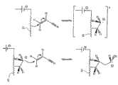
电接枝聚合物的一个特定特征是它导致在聚合物和表面之间形成真正的碳/金属共价键。该结果,是附图3中所示的反应机理的直接结果,是在导电和半导体表面上固体地附着有机片段的非常有利的路线。A specific feature of electrografted polymers is that it leads to the formation of true carbon/metal covalent bonds between the polymer and the surface. This result, a direct consequence of the reaction mechanism shown in Figure 3, is a very favorable route for the solid attachment of organic fragments on conductive and semiconducting surfaces.
然而,由于该方法是基于在表面上聚合物的就地合成,主要在合适的前体单体的性质、以及因此可以通过该方法沉积在导电或半导体表面上的聚合物的类型方面产生限制。However, since the method is based on the in situ synthesis of polymers on the surface, limitations arise mainly with regard to the nature of suitable precursor monomers, and thus the types of polymers that can be deposited on conductive or semiconducting surfaces by this method.
-仅可以通过亲核或亲电子攻击而开裂的乙烯基单体和环状分子如内酯,可以与这些机理相容,原因是它们是唯一能够通过离子化学生长而聚合的分子。- Vinyl monomers and cyclic molecules such as lactones, which can only be cleaved by nucleophilic or electrophilic attack, are compatible with these mechanisms since they are the only molecules capable of polymerizing by ionic chemical growth.
-在上面的单体中,仅仅含有吸电子或给电子基团的那些可以充分激活这些前体,从而使该生长有效。- Of the above monomers, only those containing electron-withdrawing or electron-donating groups can sufficiently activate these precursors for this growth to be effective.
-由于该生长相对地受到表面接近度的阻碍,因此通常观察到电接枝仅产生相对短的聚合物链,这排除了使用该方法附着具有大分子量的聚合物结构(尽管符合要求)。- Since the growth is relatively hindered by the proximity of the surface, electrografting is generally observed to produce only relatively short polymer chains, which precludes the attachment of polymeric structures with large molecular weights using this method (although desirable).
这些限制导致电接枝不能提供在表面上附着任意类型的聚合物材料的体系溶液。These limitations lead to the inability of electrografting to provide a systemic solution for attaching any type of polymeric material on the surface.
然而,电接枝是解决有机/导体界面的问题的有益方式,例如使得它们用作电接枝膜/导电聚合物混合膜的生长基质,以便同时利用金属上电接枝链的高粘性,以及某些导电聚合如聚吡咯物的防腐蚀性能,它们本身显示对它们所基于合成的底物的低粘性,如附属文献列表的文献[6]中所述。由这些作者形成的涂层是复合涂层,其中在金属/有机界面上带有导电聚合物,以确保其防腐蚀性能,并通过电接枝聚合物将其“胶囊化”,这可以通过X-射线光电分光光度法(XPS)的表面分析证实。However, electrografting is a beneficial way to address issues at the organic/conductor interface, such as enabling them to be used as growth substrates for electrografted films/conducting polymer hybrid films, in order to simultaneously take advantage of the high viscosity of electrografted chains on metals, and The anti-corrosion properties of certain conductive polymers such as polypyrroles, which themselves exhibit low viscosity to the substrates on which they are synthesized, are described in [6] of the attached literature list. The coatings formed by these authors are composite coatings with conductive polymers at the metal/organic interface to ensure their anti-corrosion properties and "encapsulated" by electrografted polymers, which can be obtained by X - Surface analysis confirmation by X-ray photoelectric spectrophotometry (XPS).
方法的另一实例是电沉积聚合物,或者电泳,它是主要通过静电相互作用将溶液中存在的带电聚合物(聚电解质)吸引到导电或半导体表面上的电化学过程,如所附文献列表的文献[7]中所述。该方法可以在导电或半导体表面上获得相对粘性的涂层,即使不存在聚合物/金属键会获得对工作条件敏感的界面。然而,它限于带电聚合物,并且经电控制反应处理,其中厚度密切依赖于局部电流。因此通常观察到低厚度的相当大的不均匀沉积,仅在通常为几微米或更大的厚层观察到拉平效应。Another example of a method is electrodeposition of polymers, or electrophoresis, which is an electrochemical process that attracts charged polymers (polyelectrolytes) present in solution onto conductive or semiconducting surfaces, primarily through electrostatic interactions, as described in the attached list of literature described in the literature [7]. This approach can achieve relatively sticky coatings on conductive or semiconducting surfaces, even in the absence of polymer/metal bonds that would yield interfaces sensitive to operating conditions. However, it is limited to charged polymers and processed by electrically controlled reactions, where the thickness is closely dependent on the local current. A rather large inhomogeneous deposition is therefore generally observed at low thicknesses, with a leveling effect only observed in thick layers, typically a few micrometers or greater.
对于称作为聚合物的沉积,对在导电和半导体表面上沉积金属而言主要有两个主要路线相区别:For deposition known as polymers, two main routes are distinguished for depositing metals on conductive and semiconducting surfaces:
-图示进行电化学路径,或者电沉积(“电镀”或“电化学沉积”(ECD)),由此还原希望沉积在目标表面上的含金属盐的溶液,将其用作工作电极。该溶液的电解能够将目标金属沉积在表面上,前提是所需的还原电压与所选溶剂和所选载体电解质相容。然而,通常观察到,需要各种添加剂例如表面活性剂、光泽剂等以获得高质量的均匀沉积。此外,即使使用这些添加剂,这种方法会突然地进行因此产生弱的界面,除非进行高温退火操作使得界面熔融。而且,金属在半导体表面的电沉积,特别是当金属被精细操作并且当需要结合精细操作和沉积时,是不可能的,这尤其是因为电沉积反应是电控制反应,因此对电阻降拓扑(ohmic drop topology)特别敏感。该问题产生于例如参照附表的文献[8]中所述的用于微电子中制备互联铜网络的Damascene过程:在越来越窄的蚀刻区中沉积铜轨道,它目前为约100纳米的数量级,用由半导体材料,例如氮化钛或氮化钽构成的阻挡层覆盖,其电阻率是几百微欧姆厘米。尽管这种电阻率适中,但是沉积均匀性的问题仅可以通过CVD或PVD(物理蒸汽沉积)加入非常细的铜亚层(晶种层)为代价以提高通过电沉积的铜沉积的均匀性来解决。- Schematically perform an electrochemical route, or electrodeposition ("electroplating" or "electrochemical deposition" (ECD)), whereby a metal salt-containing solution desired to be deposited on a target surface is reduced, using it as a working electrode. Electrolysis of this solution enables the deposition of the target metal on the surface, provided the required reduction voltage is compatible with the chosen solvent and chosen support electrolyte. However, it is generally observed that various additives such as surfactants, gloss agents, etc. are required to obtain high quality uniform deposition. Furthermore, even with these additives, the process proceeds abruptly and thus produces a weak interface unless a high temperature annealing operation is performed to melt the interface. Moreover, the electrodeposition of metals on semiconductor surfaces, especially when the metals are finely manipulated and when a combination of fine manipulation and deposition is required, is not possible, especially because the electrodeposition reaction is an electrically controlled reaction, and is therefore of great importance to the drop-resistance topology ( ohmic drop topology) are particularly sensitive. This problem arises from the Damascene process used for the preparation of interconnected copper networks in microelectronics as described, for example, in [8] with reference to the appended table: copper tracks are deposited in increasingly narrow etch regions, which are currently about 100 nanometers order of magnitude, covered with a barrier layer of semiconductor material such as titanium nitride or tantalum nitride, the resistivity of which is several hundreds of microohm-centimeters. Despite this moderate resistivity, the problem of deposition uniformity can only be resolved by adding a very fine copper sublayer (seed layer) by CVD or PVD (Physical Vapor Deposition) at the expense of improving the uniformity of copper deposition by electrodeposition solve.
-喷雾法,例如CVD、PVD以及相关方法如PACVD和ALCVD(原子层CVD)。如上所述,这些方法用于制备在Damascene过程中通过电沉积沉积铜的晶种层。然而,通过CVD或PVD在铜的晶种层与半导体表面之间构成的被称为阻挡层的界面是陡变的。铜对这些阻挡层材料非常低的亲和力在铜/阻挡层界面产生粘性问题,特别是在非常低的厚度(<50nm)的情况下。这些粘性问题是退火时界面破裂的机械约束的根源,并因此降低该方法的产率。这些问题目前仍然是Damascene过程成功的关键和主要挑战,特别是在0.1μm和更低的非常细的蚀刻时,并且需要补充装置来强化晶种层与半导体阻挡层材料之间的界面。- Spray methods such as CVD, PVD and related methods such as PACVD and ALCVD (atomic layer CVD). As mentioned above, these methods are used to prepare the seed layer for depositing copper by electrodeposition in the Damascene process. However, the interface called a barrier layer formed between the copper seed layer and the semiconductor surface by CVD or PVD is abrupt. The very low affinity of copper for these barrier materials creates stickiness problems at the copper/barrier interface, especially at very low thicknesses (<50nm). These stickiness problems are the source of mechanical constraints for interfacial rupture during annealing and thus reduce the yield of the process. These issues currently remain the key and main challenge for the success of the Damascene process, especially at very fine etches of 0.1 μm and lower, and supplementary devices are required to strengthen the interface between the seed layer and the semiconductor barrier material.
至于绝缘固体的沉积,它们不是如上述的那些的聚合物的材料。特别是,在如下情况下考虑离子固体,例如不溶性盐如卤化银、羟基磷灰石、碱金属或碱土金属碳酸盐、碱金属或碱土金属酒石酸盐、碱金属或碱土金属柠檬酸盐、碱金属或碱土金属草酸盐,等等。As for the deposition of insulating solids, they are not polymeric materials like those mentioned above. In particular, ionic solids are considered in the case of, for example, insoluble salts such as silver halides, hydroxyapatite, alkali metal or alkaline earth metal carbonates, alkali metal or alkaline earth metal tartrates, alkali metal or alkaline earth metal citrates, alkali Metal or alkaline earth metal oxalates, etc.
本来,这些材料具有与导体和半导体材料差别非常大的电子结构,以至于难以想到促进离子绝缘体/导体或离子绝缘体/半导体界面处的结合。在这些沉淀盐和导体或半导体表面之间的界面因此保持陡变,并且很难控制。Originally, these materials have electronic structures so different from those of conductors and semiconductors that promoting bonding at the ionic insulator/conductor or ionic insulator/semiconductor interface is difficult to conceive. The interface between these precipitated salts and the conductor or semiconductor surface thus remains abrupt and difficult to control.
已知例如在医学植入物,特别是臀修复或牙植入物的钛表面上产生粘合和可再生沉积物如钙羟基磷灰石的涂层是有益的,一方面产生阻挡层并防止金属腐蚀和金属离子的扩散,它是发炎的根源,并且另一方面在修复的表面提供足够仿生的范围以促进骨细胞(例如成骨细胞和破骨细胞)的粘附和生长并通过周围组织再定位植入物。已知需要将固体高质量地粘附在金属的表面上,特别是在修复本身经受机械应力的工作条件下,例如在臀修复的情况下。It is known that coatings such as calcium hydroxyapatite that produce adhesive and regenerative deposits such as calcium hydroxyapatite on titanium surfaces of medical implants, especially hip restorations or dental implants are beneficial, on the one hand creating a barrier layer and preventing Metal corrosion and diffusion of metal ions, which are a source of inflammation and on the other hand provide sufficient biomimetic coverage on the repaired surface to facilitate the adhesion and growth of bone cells (such as osteoblasts and osteoclasts) and pass through the surrounding tissue Reposition the implant. It is known that there is a need for high-quality adhesion of solids to metallic surfaces, especially in working conditions where the repair itself is subject to mechanical stress, for example in the case of hip repairs.
现在,经常观察到,在工作条件下,臀修复的陶瓷部分破碎,局部释放微粒和纳米颗粒,它们是局部发炎的根源,并可能必需手术更换。Now, it is often observed that under working conditions ceramic parts of hip restorations fracture, releasing microparticles and nanoparticles locally, which are a source of local inflammation and may necessitate surgical replacement.
在前述情况下,目前进行如下操作:In the foregoing cases, the following operations are currently performed:
-通过血浆喷射在金属植入物,例如臀修复最后阶段沉积磷酸钙;- deposition of calcium phosphate in metal implants, e.g. in the final stages of hip repair, by plasma injection;
-通过在模拟隙间流体的性能的流体(“模拟体液”)中浸泡以形成含碳酸盐的磷灰石层。- Formation of a carbonate-containing apatite layer by immersion in a fluid that simulates the properties of an interstitial fluid ("simulated body fluid").
这些方法基本上采用常规表面处理并且特征在于将固体沉淀在表面上,任选地经过预处理。由于上面所谓的电子结构的差异的原因,因此对在这些固体和导体或半导体表面之间的界面强化存在问题,并且上述缺陷未解决。These methods basically employ conventional surface treatment and are characterized by the precipitation of solids on the surface, optionally with pretreatment. Due to the above-mentioned differences in the electronic structure, there are problems with interface strengthening between these solids and conductor or semiconductor surfaces, and the above-mentioned deficiencies are not resolved.
因此真正需要新工艺来涂布表面,从而克服现有技术的工艺中的上面提及的许多问题和缺陷。There is therefore a real need for new processes to coat surfaces that overcome many of the above mentioned problems and drawbacks in prior art processes.
发明简述Brief description of the invention
本发明的目的特别是提供一种方法,它尤其满足上述的所有需要求,满足上述标准和要求,没有现有技术方法的缺陷、限制、失败和不利,并且克服了现有技术方法中特别是与表面性质和打算涂布所述表面的涂层的性质有关的问题。The object of the present invention is in particular to provide a method which in particular meets all the above-mentioned requirements, meets the above-mentioned standards and requirements, does not have the defects, limitations, failures and disadvantages of the prior art methods, and overcomes the problems in the prior art methods especially Questions relating to the nature of the surface and the nature of the coating intended to coat said surface.
上面所列材料,即聚合物和有机大分子、可以电沉积的固体,特别是金属、以及最终可以通过沉淀或者通过重力沉积的固体,具有差别非常大的结构和行为。本发明的一个目的是提出一种将它们牢固地固定在表面以将它们附着于其上的常用方法。The materials listed above, namely polymers and organic macromolecules, solids that can be electrodeposited, especially metals, and solids that can eventually be deposited by precipitation or by gravity, have very different structures and behaviors. An object of the present invention is to propose a common method of fastening them firmly to surfaces to attach them thereto.
本发明的方法是用第一材料和第二材料涂布表面的方法,包括以下步骤:The method of the present invention is a method for coating a surface with a first material and a second material, comprising the steps of:
-将第一材料放置在所述表面上,- placing a first material on said surface,
-在将所述第一材料放置在所述表面的步骤的同时或者在该步骤之后,将第二材料的前体插入到第一材料中,- simultaneously with or after the step of placing said first material on said surface, inserting a precursor of a second material into the first material,
-将插入到第一材料中的第二材料的前体转化成所述第二材料,使得第二材料形成于待涂布的所述表面上并且在放置在所述表面上的所述第一材料内。- converting the precursor of the second material inserted into the first material into said second material, so that the second material is formed on said surface to be coated and on said first material placed on said surface within the material.
本发明的方法可用于任意类型的表面,例如可用于上述现有技术部分提及的表面。The method of the invention can be used on any type of surface, for example the surfaces mentioned in the prior art section above.
根据本发明,一般说来,该表面是基质的表面,其上打算沉积涂层,以便应用所述基质,例如保护基质、保护其应用的环境、将其功能化等等。该表面可以是绝缘的、导电的或半导体的表面。例如可以是无机表面如金属或陶瓷表面;可以是有机表面如聚合物表面。这些表面在本上下文中也称之为“待涂布的表面”。下面给出了许多应用的实例,并且其它应用对本领域技术人员来说也是显而易见的。According to the invention, in general, this surface is the surface of the substrate on which the coating is intended to be deposited in order to apply said substrate, for example to protect the substrate, protect the environment in which it is used, functionalize it, etc. The surface may be an insulating, conducting or semiconducting surface. For example, it may be an inorganic surface such as a metal or ceramic surface; it may be an organic surface such as a polymer surface. These surfaces are also referred to in this context as "surfaces to be coated". Examples of many applications are given below, and others will be apparent to those skilled in the art.
本发明的方法尤其可以制备材料的非常粘的沉积,该材料本文下面称之为“目标材料”,在本发明的含义中它可以是在表面上的第一材料或第二材料,而通过使用现有技术方法,所述目标材料未粘附或者非常少地粘附于所述表面上。更具体地说,本发明的方法可以通过将目标材料的粘性沉积与也被称为补充材料(complementary material)的另一材料的沉积结合而制备在表面上目标材料的沉积。为了本发明的目的,如果目标材料是第一材料,那么补充材料是第二材料,反之亦然。The method of the invention makes it possible in particular to produce very viscous deposits of material, referred to herein below as "target material", which can be the first material or the second material on a surface within the meaning of the invention, whereas by using Prior art methods, the target material does not adhere or very little adheres to the surface. More specifically, the method of the invention makes it possible to prepare the deposition of a target material on a surface by combining the viscous deposition of the target material with the deposition of another material, also called complementary material. For the purposes of the present invention, if the target material is the first material, then the supplementary material is the second material, and vice versa.
特别是,根据本发明,根据在表面上沉积的顺序,将可以非常粘性地沉积在表面,特别是导电或半导体表面上的材料分成两类。In particular, according to the invention, materials that can deposit very viscously on surfaces, especially conductive or semiconducting surfaces, are divided into two categories according to the sequence of deposition on the surface.
为了本发明的目的的第一材料的类别,本文下面称之为“可层叠材料”(layerable material)或“铠装材料”(armouring material),这取决于本发明的用途。例如,它可以是能够实施本发明的本领域技术人员已知的任意聚合物或任意有机大分子。通过在待涂布的表面上获得优选以膜的形式的所述材料的沉积的任意方法来沉积有机材料是有利的。根据本发明,第一材料是可以通过选自如下的工艺有利地放置在表面上的材料:离心(“旋涂”或“旋压”)、喷雾、浸泡(“浸涂”)、电聚合、电接枝等等。例如可以提及吡咯、苯胺、噻吩、亚乙基二氧基噻吩(EDOT)、乙二胺、苯酚等聚合物,及其衍生物。这些聚合物例如适用于电聚合。还可以提及的实例包括由活化的环状乙烯基单体获得的聚合物,所述单体可以经亲核和亲电子攻击裂开。这些聚合物例如适用于电接枝。下面给出进一步的实例。The first class of materials for the purposes of the present invention is referred to herein below as "layerable material" or "armouring material", depending on the use of the present invention. For example, it may be any polymer or any organic macromolecule known to those skilled in the art capable of carrying out the invention. It is advantageous to deposit the organic material by any method which obtains a deposition of said material, preferably in the form of a film, on the surface to be coated. According to the invention, the first material is a material that can advantageously be placed on the surface by a process selected from: centrifugation ("spin coating" or "spinning"), spraying, immersion ("dip coating"), electropolymerization, Electrografting and more. For example, there may be mentioned polymers such as pyrrole, aniline, thiophene, ethylenedioxythiophene (EDOT), ethylenediamine, phenol, and derivatives thereof. These polymers are suitable, for example, for electropolymerization. Examples that may also be mentioned include polymers obtained from activated cyclic vinyl monomers which can be cleaved via nucleophilic and electrophilic attack. These polymers are suitable, for example, for electrografting. Further examples are given below.
用于本发明目的的第二材料的类别,当它强化本发明的第一材料的附着时,本文下面也称之为“增强剂”。它有益地是可以聚集在表面上的无机材料,即在表面上为如下的沉积模式:或者沉淀,即通过天然或人造重力沉积;或者结晶,例如晶体生长;或者以无定形沉积;或者以无定形或晶体形式电沉积;或者以聚集体的形式沉积或聚集。优选,第二材料是可以电沉积的材料。The class of second material used for the purposes of the present invention, when it strengthens the adhesion of the first material of the present invention, is also referred to herein below as "enhancer". It is advantageously an inorganic material that can accumulate on a surface, i.e. on a surface in a mode of deposition: either precipitation, i.e. deposition by natural or artificial gravity; or crystallization, e.g. crystal growth; or deposition in an amorphous form; or in an amorphous electrodeposited in a fixed or crystalline form; or deposited or aggregated in the form of aggregates. Preferably, the second material is an electrodepositable material.
根据本发明,“强化”材料可以与构成打算被涂布的表面的材料相同或者不同。According to the invention, the "reinforcing" material may be the same as or different from the material making up the surface to be coated.
正如阅读本发明所清楚呈现的,术语“强化”不参与第二材料在本发明的作用:具体地说,相应于第二材料的“强化”材料或者可以强化第一材料与表面的粘性,或者本身可以得到强化,或者通过第一材料强化它与表面的粘性而这种情况下为了本发明的目的,第一材料用作铠装。As is clear from reading the present invention, the term "reinforcing" does not take part in the role of the second material in the present invention: specifically, the "reinforcing" material corresponding to the second material can either strengthen the adhesion of the first material to the surface, or It may be strengthened itself, or its adhesion to the surface may be strengthened by the first material in which case, for the purposes of the present invention, the first material acts as armor.
在第二材料的类别中,在可用于本发明的材料中,可以区别如下:In the category of the second material, among the materials usable in the present invention, the following can be distinguished:
-可以电沉积的材料:它们是无机或有机材料,它们可以经电化学沉积,并且优选通过电控制反应在导电或半导体表面上沉积,即电化学反应中材料的沉积量与通过电化学沉积电池的电荷(=电流总和)有关,并且经常成比例。特别是,这些电控制的反应能够控制第二材料由其前体的沉积和/或形成。因此,第二材料的前体将有益地是该材料的离子。这些反应尤其可以是由该金属的前体离子的溶液沉积金属的反应,例如由含有铜离子的溶液沉积铜,并且类似地由各自的离子沉积锌、金、锡、钛、钒、铬、铁、钴、锂、钠、铝、镁、钾、铷、铯、锶、钇、铌、钼、钌、铑、钯、银、镉、铟、镥、铪、钽、钨、铼、锇、铱、铂、汞、铊、铅、铋、镧系和锕系;通过前体单体的电聚合沉积绝缘聚合物如乙二胺类和酚类;通过前体单体的电聚合沉积导电聚合物如吡咯、苯胺、噻吩、甲基噻吩、亚乙基二氧基噻吩(EDOT)及其衍生物;通过由含有它们的溶液电沉积来沉积聚电解质;和-Materials that can be electrodeposited: they are inorganic or organic materials that can be deposited electrochemically and preferably on conductive or semiconducting surfaces by electrically controlled reactions, i.e. the amount of material deposited in an electrochemical reaction is the same as that obtained by an electrochemical deposition cell The charge (= sum of currents) of , is related and often proportional. In particular, these electrically controlled reactions enable controlled deposition and/or formation of the second material from its precursor. Thus, the precursors of the second material will beneficially be ions of that material. These reactions may especially be those of depositing a metal from a solution of precursor ions of the metal, for example copper from a solution containing copper ions, and similarly zinc, gold, tin, titanium, vanadium, chromium, iron from the respective ions , cobalt, lithium, sodium, aluminum, magnesium, potassium, rubidium, cesium, strontium, yttrium, niobium, molybdenum, ruthenium, rhodium, palladium, silver, cadmium, indium, lutetium, hafnium, tantalum, tungsten, rhenium, osmium, iridium , platinum, mercury, thallium, lead, bismuth, lanthanides and actinides; deposition of insulating polymers such as ethylenediamines and phenols by electropolymerization of precursor monomers; deposition of conductive polymers by electropolymerization of precursor monomers such as pyrrole, aniline, thiophene, methylthiophene, ethylenedioxythiophene (EDOT) and their derivatives; deposition of polyelectrolytes by electrodeposition from solutions containing them; and
-不可以电沉积的材料:它们是可以通过沉淀、结晶、交联、聚集等在表面上沉积的材料。可以在天然和人造重力的影响下,以聚集体、球或块的形式产生沉淀。它们尤其可以是离子盐,例如羟基磷灰石、磷酸氢钙和/或磷酸氢镁、卤化银等,并且更通常地是所有不溶性盐,特别是不溶于水的盐的沉淀或结晶反应;氨基低聚物或聚合物通过双官能化合物,例如表氯醇、戊二酸酐、戊二醛或二环氧化合物的交联反应;羟基化低聚物或聚合物通过双官能化合物,例如戊二酸酐或二羧酸,例如壬二酸的交联反应;乙烯基聚合物通过聚乙烯交联剂,例如二乙烯基苯或季戊四醇四甲基丙烯酸酯的交联反应。下面给出进一步的实例。- Materials that cannot be electrodeposited: they are materials that can be deposited on a surface by precipitation, crystallization, cross-linking, aggregation, etc. Precipitation can occur in the form of aggregates, spheres or clumps under the influence of natural and artificial gravity. They may especially be ionic salts such as hydroxyapatite, calcium and/or magnesium hydrogen phosphate, silver halides, etc., and more generally all insoluble salts, especially precipitation or crystallization reactions of water-insoluble salts; amino Oligomers or polymers are crosslinked by difunctional compounds such as epichlorohydrin, glutaric anhydride, glutaraldehyde or diepoxides; hydroxylated oligomers or polymers are crosslinked by difunctional compounds such as glutaric anhydride Or dicarboxylic acid, such as azelaic acid crosslinking reaction; vinyl polymer crosslinking reaction by polyethylene crosslinking agent, such as divinylbenzene or pentaerythritol tetramethacrylate. Further examples are given below.
本发明中的术语“第二材料的前体”显然包括第二材料的单一前体或至少两种选自本文所述第二材料的前体的混合物。因此,通过上述提及的前体的混合物的溶液或浴将第二材料的前体插入到第一材料中。The term "precursor of the second material" in the present invention clearly includes a single precursor of the second material or a mixture of at least two precursors selected from the group of the second material described herein. Thus, the precursors of the second material are inserted into the first material by means of a solution or bath of a mixture of the above mentioned precursors.
当使用至少两种前体实施本发明时,可以在第一材料内进行前体向第二材料的转变,以便各种前体彼此同时或者相继独立地转变,例如通过施加合适的沉淀、电沉积等等条件。本发明的这些特定的实施方式例如可用于制备催化剂。When the invention is carried out using at least two precursors, the transformation of the precursors into the second material can be carried out within the first material so that the various precursors are transformed independently of each other simultaneously or in succession, for example by applying suitable precipitation, electrodeposition And so on. These particular embodiments of the invention are useful, for example, in the preparation of catalysts.
根据本发明,待沉积在表面上的目标材料可以属于上述两类中的一类或另一类。换句话说,如上所述,目标材料可以是为了实现本发明目的的第一材料或第二材料:According to the invention, the target material to be deposited on the surface may belong to one or the other of the above two categories. In other words, as mentioned above, the target material can be the first material or the second material for the purposes of the present invention:
例如,如果第一材料是目标材料,并且如果它是可层叠材料,其在表面上的粘性沉积是通过沉积第二材料进行或者提高的。一旦该过程结束,目标材料即在为第一材料的情况下,与第二材料一起层合在表面上。For example, if the first material is the target material, and if it is a laminable material, its adhesive deposition on the surface is performed or enhanced by depositing the second material. Once the process is complete, the target material, as it were the first material, is laminated on the surface together with the second material.
例如,同样的如果第二材料是目标材料,并且如果其在表面上的粘性沉积是通过选自上述可层叠材料的第一材料进行或者提高的,一旦该过程结束,可以说第二材料用第一材料在表面上得到强化。For example, also if the second material is the target material, and if its adhesive deposition on the surface is carried out or enhanced by the first material selected from the above-mentioned laminable materials, once the process is completed, it can be said that the second material is used with the first material. A material is strengthened on the surface.
根据目标材料是本发明的第一材料还是第二材料,实施本发明方法的原理因此经常是相同的,给出或呈现几个定量细节,使得这些术语仅仅相对于目标材料而不是能够帮助其沉积的材料,并因此相对于所需应用而不是该方法:因此在上述材料列表之间存在一对一的关系。为此在本发明的方法的定义中将它们称之为“第一”和“第二”材料。Depending on whether the target material is the first or the second material of the invention, the principles for carrying out the method of the invention are therefore often the same, given or presented with a few quantitative details, so that these terms are only relative to the target material and not able to facilitate its deposition materials, and thus with respect to the desired application rather than the method: there is thus a one-to-one relationship between the above lists of materials. For this reason they are referred to as "first" and "second" materials in the definition of the method of the present invention.
本发明的一个特别重要的方面是通过将选自这两类材料之一的目标材料的沉积与选自另一类的补充材料的组合,从而获得目标材料的非常好的粘性。A particularly important aspect of the invention is to obtain a very good adhesion of the target material by combining the deposition of the target material from one of these two classes of materials with a supplementary material from the other class.
因此,根据本发明方法的第一实施方式,第一材料可以如通过化学吸附或电接枝附着于表面上,以铠装材料的形式用作附着物或者通过该铠装材料和表面之间产生的界面连接强化第二材料与表面的附着:根据本发明,描述为第二材料在表面上的沉积用第一材料得到强化。该实施方式图示描述于附图1。该实施方式例如可以如下方式进行:第一材料是聚合物如有机聚合物,电接枝于表面上。第二材料是如以层的形式沉积于该聚合物内的金属。该聚合物因此用作附着金属层的“铠装”。根据该实施方式,第一材料可以埋在第二材料中。Thus, according to a first embodiment of the method according to the invention, the first material can be attached to the surface, for example by chemisorption or electrografting, be used as an attachment in the form of an armor material or by creating a barrier between the armor material and the surface. The interfacial connection of enhances the adhesion of the second material to the surface: According to the invention, it is described that the deposition of the second material on the surface is enhanced with the first material. This embodiment is schematically described in Figure 1 of the accompanying drawings. This embodiment can be carried out, for example, in that the first material is a polymer, such as an organic polymer, electrografted onto the surface. The second material is a metal deposited as a layer within the polymer. The polymer thus acts as an "armor" to which the metal layer is attached. According to this embodiment, the first material may be embedded in the second material.
根据本发明方法的第二实施方式,第一材料例如通过化学吸附或电接枝可以附着于表面上,或者以层状材料的形式以非粘性方式简单地沉积在表面上,并且在其内形成的第二材料通过第二材料和表面之间产生的界面相连而强化第一材料与表面的附着:根据本发明,描述为第一材料在表面上的附着或沉积用第二材料得到强化。该实施方式保证第一材料比其单独存在时其与表面之间存在的更固态的界面。可以与前面相同的方式描述该实施方式,但是由于目标材料是第一材料,务必确保在由前体形成第二材料期间它会不被第二材料埋入。例如,由于第二材料在为强化材料的情况下,例如通过电控制的反应沉积,因此在其电沉积期间可以有益地控制电荷,使得其在第一材料或可层叠材料内的生长仅在其内发生并且不包埋所述材料。通过本发明的该实施方式,第一材料的根部,在这种情况下它是聚合物,原样“浸泡”在第二材料中,优选这样是因为其与表面的界面相容性。该实施例图示于附图2中。According to a second embodiment of the method according to the invention, the first material can be attached to the surface, for example by chemisorption or electrografting, or simply deposited in a non-adhesive manner in the form of a layered material on the surface and formed therein The second material strengthens the adhesion of the first material to the surface through the interfacial connection created between the second material and the surface: According to the invention, it is described that the adhesion or deposition of the first material on the surface is strengthened by the second material. This embodiment ensures a more solid interface between the first material and the surface than would exist between it and the surface if it were present alone. This embodiment can be described in the same way as before, but since the target material is the first material, it must be ensured that it will not be embedded by the second material during formation of the second material from the precursor. For example, since the second material is deposited, e.g., by an electrically controlled reaction, in the case of a strengthening material, charge can be advantageously controlled during its electrodeposition such that its growth within the first or stackable material is only within its occurs within and does not embed the material. With this embodiment of the invention, the root of the first material, which in this case is a polymer, is "soaked" as it is in the second material, which is preferred because of its interfacial compatibility with the surface. This embodiment is shown schematically in FIG. 2 .
发明人对本发明方法的第二实施方式建议命名为“电化学压条”(electrochemical layering),压条是植物学中用于由枝通过将它们插入到地下使它们从土壤伸出再造根的方法。The inventors propose the name "electrochemical layering" for a second embodiment of the method of the present invention, layering is a method used in botany to re-root shoots from the soil by inserting them into the ground.
根据本发明人特别优选的一个模式,本发明的方法可以在为导电或半导体表面的表面上进行,第一材料是乙烯基聚合物,第二材料是金属,并且该金属的前体是该金属的离子。According to a mode particularly preferred by the inventors, the method of the invention can be carried out on a surface which is a conductive or semiconducting surface, the first material being a vinyl polymer, the second material being a metal, and the precursor of the metal being the metal of ions.
根据本发明的方法,将第二材料的前体插入到第一材料中的步骤是一个决定性步骤。特别是,它是在第一材料的前体插入到第二材料中以便之后能够在其中转变成第二材料的步骤期间进行。对该第二步而言,可以使用属于本发明内容的许多工艺。它们包括从简单地将第二材料的前体与放置在表面上的第一材料接触,例如通过将放置在表面上的第一材料浸泡在所述前体的合适溶液中,到更复杂的工艺例如使用电解浴。According to the method of the invention, the step of inserting the precursor of the second material into the first material is a decisive step. In particular, it is carried out during the step of intercalation of the precursor of the first material into the second material in order to be able to transform into the second material thereafter. For this second step, a number of processes that fall within the context of the present invention can be used. They range from simply bringing a precursor of the second material into contact with the first material placed on the surface, for example by soaking the first material placed on the surface in a suitable solution of said precursor, to more complex processes For example using an electrolytic bath.
如果不能容易地向第一材料中插入第二材料的前体,或者如果该插入必须被促进,或者甚至被强制,根据本发明,可以使用既为第二材料的前体的溶剂或运输物,又为膨胀第一材料的溶剂和/或溶液的插入溶液(insertion solution),所述插入溶液包括第二材料的前体。If it is not easy to insert into the first material a precursor of the second material, or if this insertion has to be facilitated, or even forced, according to the invention a solvent or transport which is also a precursor of the second material may be used, Also an insertion solution of a solvent and/or solution that swells the first material, said insertion solution comprising a precursor of the second material.
例如,当第一材料为聚合物时该溶剂是该聚合物的溶剂。For example, when the first material is a polymer, the solvent is a solvent for the polymer.
术语“膨胀第一材料的溶液”是指插入到第一材料中并展开其结构使得将其含有的第二材料的前体插入到第一材料中的溶液。例如,它可以是例如水合第一材料的水溶液。已知有经水膨胀的乙烯基聚合物,特别是不溶于水的聚(4-乙烯基吡啶),P4VP;或者溶于水的聚甲基丙烯酸羟基乙酯,PHEMA,并因此也被该溶剂膨胀。这些聚合物可以用作本发明的第一材料。The term "solution that swells the first material" refers to a solution that is inserted into the first material and unfolds its structure so that the precursors of the second material it contains are inserted into the first material. For example, it may be, for example, an aqueous solution of the hydrated first material. Water-swellable vinyl polymers are known, in particular poly(4-vinylpyridine), P4VP, which is insoluble in water; or polyhydroxyethylmethacrylate, PHEMA, which is soluble in water, and are therefore also swell. These polymers can be used as the first material in the present invention.
该插入溶液也是可以传送第二材料的前体进入第一材料的溶液。因此它是能够充分溶解或分散实施本发明的前体的溶液。特别是,在第二材料为不溶性盐的情况下,该溶液优选必须能够充分分散第二材料的前体以能够将其插入到第一材料中。The intercalation solution is also a solution that can deliver the precursor of the second material into the first material. It is thus a solution capable of sufficiently dissolving or dispersing the precursors for the practice of the invention. In particular, where the second material is an insoluble salt, the solution preferably must be capable of dispersing the precursor of the second material sufficiently to enable its insertion into the first material.
该插入溶液因此以许多标准的函数来选择。其中,可以提及:作为表面的函数:例如为避免例如实施本发明期间表面氧化的化学相互作用;作为第一材料的函数:以便该溶液不从沉积第一材料的表面上除去第一材料;作为第二材料的前体的函数:它必须能够溶解第二材料的前体,而且也能够将其转变成第二材料;作为第二材料的函数:必须能够在第一材料内形成第二材料,并且特别是实施其沉积过程,例如第二材料的电沉积。The intercalation solution is thus chosen as a function of a number of criteria. Among others, mention may be made of: as a function of the surface: for example to avoid chemical interactions such as oxidation of the surface during the implementation of the invention; as a function of the first material: so that the solution does not remove the first material from the surface on which it is deposited; As a function of the precursor of the second material: it must be able to dissolve the precursor of the second material and also convert it into the second material; as a function of the second material: it must be able to form the second material within the first material , and in particular to carry out its deposition process, such as electrodeposition of a second material.
例如,由于现有技术含有大量如下信息,首先是关于通过电沉积由水溶液制得金属膜,其次是关于其在水中的溶解性,根据本发明优选的适当插入溶液是水溶液,特别是当第一材料是可以用水膨胀的聚合物时,例如以电接枝铠装膜的形式。下面描述其它插入溶液和将第二材料的前体插入到第一材料中的方法。本领域技术人员还可以选择其它合适插入溶剂实施本发明,例如用上述“强化”材料类的前体。For example, since the prior art contains a great deal of information, firstly about the production of metal films from aqueous solutions by electrodeposition, and secondly about their solubility in water, the preferred suitable intercalation solution according to the invention is an aqueous solution, especially when the first When the material is a water-swellable polymer, for example in the form of an electrografted armor film. Other intercalation solutions and methods for intercalating precursors of the second material into the first material are described below. Those skilled in the art can also choose other suitable intercalation solvents to implement the present invention, such as using the precursors of the above-mentioned "strengthening" materials.
根据本发明方法的第三实施方式,通过既包括所述第一材料或所述第一材料的前体与第二材料的前体的溶液,包括向放置在所述表面上的第一材料中插入第二材料的前体的步骤可以与包括将第一材料放置在所述表面上的步骤同时进行。当其难以发现膨胀放置在基质上的第一材料的插入溶液时该实施方式特别有益。因此,在将第一材料放置在基质上的第一步期间,将第二材料的前体带入到第一材料中,并且当将第一材料放置在表面上时,采用本发明的方法的步骤,在所述第一材料内将第二材料的前体转变成所述第二材料。According to a third embodiment of the method according to the invention, by introducing into the first material placed on the surface a solution comprising both the first material or the precursor of the first material and the precursor of the second material, The step of inserting a precursor of the second material may be performed simultaneously with the step comprising placing the first material on said surface. This embodiment is particularly beneficial when it is difficult to find an intercalation solution that swells the first material placed on the matrix. Thus, during the first step of placing the first material on the substrate, the precursor of the second material is brought into the first material, and when the first material is placed on the surface, the method of the present invention is employed. and converting a precursor of a second material into said second material within said first material.
本发明的转变步骤也是重要的,这是由于它必须在待涂布的表面上和在第一材料内能够将第二材料的前体转变成所述第二材料。上面已经描述了该转变的模式并将在下面更详细地描述。优选,第二材料的前体可以经选自电沉积和沉淀的工艺转变成所述相应的第二材料。The conversion step of the invention is also important, since it must be able to convert the precursor of the second material into said second material, both on the surface to be coated and within the first material. The mode of this transition has been described above and will be described in more detail below. Preferably, the precursor of the second material can be converted into said corresponding second material via a process selected from electrodeposition and precipitation.
本发明的方法因此可以包括,一旦确定打算涂布的表面和目标材料,就选择适宜的补充材料,并且还选择根据本发明方法选择沉积这两种材料各自的方法,使得能够制备所述目标材料与所述表面非常强的附着。The method of the invention may thus comprise, once the surface to be coated and the target material have been identified, selecting a suitable supplementary material and also selecting a method of depositing each of these two materials according to the method of the invention, enabling the preparation of said target material Very strong adhesion to the surface.
在实施本发明的第一实施例中,根据上述第一实施方式,其中希望在基质的表面,例如半导体(B)上沉积目标材料如为上面第二材料类别中的金属材料(A),本发明的方法可以包括以下步骤:In implementing the first embodiment of the present invention, according to the above-mentioned first embodiment, wherein it is desired to deposit the target material on the surface of the substrate, such as semiconductor (B), such as the metal material (A) in the second material category above, the present The inventive method may include the following steps:
-选择铠装材料,或者本发明含义内的第一材料,例如聚合物;- selection of an armor material, or a first material within the meaning of the invention, such as a polymer;
-选择在表面如半导体(B)上沉积铠装材料的方法;在该实施例中,该沉积方法大大地决定了目标材料如金属(A)与表面,在这种情况下为半导体(B)之间连接的牢固性。根据本发明,本领域技术人员当然可以以该牢固性标准的函数来选择该方法,也可以基于其它考虑,特别是基于如以膜形式的所需成层材料的厚度,基于该材料的厚度所需的均匀性,基于成本等。如果铠装材料是可以电接枝在表面上的聚合物,例如半导体B,由于该方法可以在聚合物和导体或半导体之间产生共价化学键,因此可以获得铠装材料与表面如半导体B之间非常牢固的固定;- choose the method of depositing the armor material on a surface such as a semiconductor (B); in this embodiment, the deposition method largely determines the target material such as a metal (A) and the surface, in this case a semiconductor (B) The firmness of the connection. According to the invention, the person skilled in the art can of course choose the method as a function of this firmness criterion, but also on the basis of other considerations, in particular based on the thickness of the desired layered material in film form, based on the thickness of the material. required uniformity, based on cost etc. If the armor material is a polymer that can be electrically grafted on the surface, such as semiconductor B, since this method can generate covalent chemical bonds between the polymer and the conductor or semiconductor, it is possible to obtain very firm fixation;
-选择沉积本发明的含义内的第二材料的方法,在这种情况下为金属A,以便其可以与沉积第一材料,铠装材料的方法相容。术语“相容性“是指该方法优选能够在铠装材料内生长强化材料:假设第二材料的前体首先可以插入,即扩散在铠装材料或第一材料内,例如内部,并且该方法可用于在铠装材料内形成第二材料;- choose the method of depositing the second material within the meaning of the invention, in this case metal A, so that it can be compatible with the method of depositing the first material, the armoring material. The term "compatibility" means that the method is preferably capable of growing reinforcement material within the armoring material: it is assumed that the precursor of the second material can first intercalate, i.e. diffuse, within the armoring material or the first material, e.g. internally, and the method Can be used to form a second material within the armor material;
-如上所述实施本发明的方法:如果第二材料是金属,使用该金属(A)的金属离子作为第二材料的前体,有益地溶解在用作铠装材料如聚合物的溶剂和/或膨胀剂中,形成第二材料的前体的溶液;该溶液能够将前体的离子在聚合物内扩散,之后,例如,采用电类型的方法如电沉积(电镀或电化学沉积(ECD)),在聚合物内形成金属(A)。由于该方法经电控制,因此在聚合物形成该铠装材料的该实施例中,在其表面上进行之前,控制电荷能够有益地监控在第一材料的整个厚度上进行的金属(A)的生长。- the method of carrying out the invention as described above: if the second material is a metal, using the metal ion of this metal (A) as a precursor of the second material, advantageously dissolved in a solvent used as an armor material such as a polymer and/ or swelling agent, forming a solution of the precursor of the second material; this solution is capable of diffusing the ions of the precursor within the polymer, after which, for example, by means of an electrical type such as electrodeposition (electroplating or electrochemical deposition (ECD) ), forming metal (A) within the polymer. Since the process is electrically controlled, in this embodiment where the polymer forms the armor material, controlling the charge can beneficially monitor the metal (A) ablation that occurs throughout the thickness of the first material before proceeding on its surface. grow.
以这种方式,可层叠材料即聚合物或第一材料,通过铠装材料和半导体(B)之间产生的界面相连,最终埋入用作“铠装”附着于金属表面(B)上的金属(A)中:在第一材料是金属(A)和表面是半导体的情况下,第一材料在表面上的沉积,据信被为聚合物的第二材料所强化。在附图1中描述了本应用实例。In this way, the layerable material, i.e. the polymer or the first material, is connected through the interface created between the armor material and the semiconductor (B), and is eventually embedded as an "armor" attached to the metal surface (B). In Metal (A): Where the first material is metal (A) and the surface is a semiconductor, the deposition of the first material on the surface is believed to be enhanced by the second material being a polymer. The present application example is described in
例如,在下面的“实施例”中证实,电沉积在金表面上的铜层的粘合或者在金属表面上的氯化银的膜的粘合,出人意料地,通过提供在两种金属之间或者金属与氯化银之间的界面埋入的聚合物强化的预处理所强化。For example, it is demonstrated in the following "Examples" that the adhesion of a layer of copper electrodeposited on a gold surface or of a film of silver chloride on a metal surface, surprisingly, by providing Or strengthened by pre-treatment of polymer reinforcement embedded in the interface between metal and silver chloride.
在本发明的第二应用实施例中,根据上述第二个实施方式,其中希望在表面,例如导电基质的表面如由金属制得的导电基质的表面上沉积聚合物(P),除了最终实施步骤之外,该方法的原理基于与上述相同的步骤。具体地说,优选在该最终步骤中,如上所述,控制第二材料在第一材料内的生长以使它不埋没该第二材料。In the second application example of the present invention, according to the above-mentioned second embodiment, wherein it is desired to deposit the polymer (P) on a surface, for example, a surface of a conductive substrate such as a conductive substrate made of a metal, except for the final implementation The principle of the method is based on the same steps as above, except for the steps. In particular, preferably in this final step, as described above, the growth of the second material within the first material is controlled so that it does not bury the second material.
例如,在下面“实施例”部分证实,通过本发明的第二实施方式,可以出人意料地将沉积的聚(4-乙烯基吡啶)(P4VP)膜通过离心附着于金表面上,且它能经受其溶剂中的一种的充分冲洗,而在没有本发明的处理的情况下,通过相同冲洗将去除相同表面上的P4VP膜。For example, as demonstrated in the "Examples" section below, by the second embodiment of the present invention, a deposited poly(4-vinylpyridine) (P4VP) film can surprisingly be centrifuged onto a gold surface, and it can withstand Sufficient rinsing of one of its solvents, while without the treatment of the present invention, would remove the P4VP film on the same surface by the same rinsing.
根据本发明,当目的是在本发明的方法的实施结束时目标材料是存在于表面上的第一材料和第二材料中的仅一种时,将采用本文下面所述的方法,或者使得第一材料从第二材料显现,或者使得第二材料浸泡或者覆盖第一材料。According to the invention, when the object is that the target material is only one of the first material and the second material present on the surface at the end of the implementation of the method of the invention, the method described herein below will be used, or such that the second A material emerges from a second material, either so that the second material soaks or covers the first material.
有益地,根据本发明,目标材料显现或者覆盖取决于本发明所选的实施方式,例如通过本发明的方法厚度至少等于两种材料在表面上形成的总厚度的20%,接着铠装或层叠。该显现部分的厚度,显而易见,取决于该表面打算的用途。Advantageously, according to the invention, the target material is revealed or covered depending on the selected embodiment of the invention, for example by the method of the invention in a thickness at least equal to 20% of the total thickness of the two materials formed on the surface, followed by armoring or lamination . The thickness of the display part, obviously, depends on the intended use of the surface.
通过实施本发明方法由第一材料和第二材料在表面上形成的涂层的厚度通常在1nm-100μm之间。显然这取决于所用材料的性质和所需的涂层类型。The thickness of the coating formed on the surface from the first material and the second material by carrying out the method of the present invention is generally between 1 nm and 100 μm. Obviously this depends on the nature of the materials used and the type of coating required.
通过本发明方法获得的涂层因此包括混合的第一材料和第二材料,它们有或者没有化学键或者有或没有相互作用,这取决于所用材料的化学性质。The coating obtained by the method of the invention thus comprises a mixture of first and second materials, with or without chemical bonds or interactions, depending on the chemical nature of the materials used.
本发明的方法因此具有许多应用,本领域技术人员通过阅读本说明书就可以发现。The method of the invention thus has many applications, as will be apparent to those skilled in the art upon reading this specification.
在这些应用中,可以提及的非限制性实例包括如下:Among these applications, non-limiting examples that may be mentioned include the following:
能够在导电或半导体基质与金属之间实现界面强化,例如通过以附图1所述的方式在基质上预接枝的聚合物铠装。该应用对特别是在微电子的铜互连中、根据Damascene或Dual Damascene过程中铜/防扩散层界面如TiN、TaN、TiNSi等的机械强化是有益的。Interfacial strengthening between a conductive or semiconducting substrate and a metal can be achieved, for example, by a polymer armor pre-grafted on the substrate in the manner described in FIG. 1 . This application is beneficial for the mechanical strengthening of copper/diffusion barrier interfaces such as TiN, TaN, TiNSi, etc., especially in copper interconnects for microelectronics according to Damascene or Dual Damascene processes.
更常见的是在金属/金属、金属/导电聚合物、导电聚合物/半导体或金属/半导体界面的粘合亚层提供有益的替代。More commonly, adhesion sublayers at metal/metal, metal/conducting polymer, conducting polymer/semiconductor, or metal/semiconductor interfaces provide a beneficial alternative.
例如,还能够在导电或半导体基质,特别是用于汽车防腐蚀、光学部件、流行物品、机械润滑、“弹抛片”(flip-clip)聚合物应用的热熔融聚合物层的沉积、或者另外用于功能化传感器的敏感部件,上沉积非常粘的有机层。因此它也涉及本发明的方法在金属表面的防腐蚀处理中的用途。For example, it is also possible to deposit layers of hot-melt polymers on conductive or semiconducting substrates, especially for automotive corrosion protection, optical components, fashion items, mechanical lubrication, "flip-clip" polymer applications, or Also used to functionalize the sensitive part of the sensor, on which very sticky organic layers are deposited. It therefore also relates to the use of the method according to the invention for the anticorrosion treatment of metal surfaces.
例如,也可以在导电可植入物品上沉积非常粘的有机层,例如沉积生物相容的聚合物和/或储槽用于包封和释放活性分子,例如在整形外科中保持移植的印记、或者血管植入物(展幅)、蜗形植入电极、导管引导(引导线)、矫正术植入物,特别是臀修补物和牙植入物。因此它也涉及本发明的方法用于可以植入到体内的物品的表面处理的用途。For example, it is also possible to deposit very viscous organic layers on conductive implantable items, such as depositing biocompatible polymers and/or reservoirs for encapsulation and release of active molecules, such as in orthopedics to maintain imprints of implants, Or vascular implants (stents), cochlear implant electrodes, catheter guides (guide wires), orthopedic implants, especially hip prostheses and dental implants. It therefore also relates to the use of the method according to the invention for the surface treatment of objects which can be implanted in the body.
例如,也可以沉积非常粘的有机层,例如沉积生物大分子,或者带有或包封有生物分子的大分子如肽、蛋白质、多糖、寡核苷酸或者DNA或RNA片段,特别是用于生产DNA或蛋白质生物芯片的用途。因此它也涉及本发明的方法用于制备生物芯片的用途。For example, very viscous organic layers can also be deposited, for example biomacromolecules, or macromolecules carrying or encapsulating biomolecules such as peptides, proteins, polysaccharides, oligonucleotides or DNA or RNA fragments, in particular for Use in the production of DNA or protein biochips. It therefore also relates to the use of the method of the invention for the preparation of biochips.
本发明的方法还能够制备催化剂,例如通过使用上述金属前体或其混合物如铑、铂、钯、钴、铜等前体或其混合物作为第二材料的前体。在该应用中,第一材料可以是本文提及的之一,有益地是具有络合第二材料前体的配体的聚合物,例如聚(4-乙烯基吡啶)(P4VP)以及带有半胱氨酸基团的任意聚合物,它可用于使催化剂的盐如钯盐附着于表面上。在第一材料的膜内还原,并且任选地可以将有机残余物烧结之后,催化剂以其金属形式获得,例如钯金属以膜形式或者以金属聚集体的形式。由此获得的催化剂特别具有如下优点:对无电方法而言,引发不同材料的层沉积,所述材料特别是应用于与微电子有关的铜(例如参见:S.James、H.Cho等,“Electroless Cu for VLSI”,MRSBulletin,20(1993)31-38)。The method of the invention also enables the preparation of catalysts, for example by using the above mentioned metal precursors or mixtures thereof such as rhodium, platinum, palladium, cobalt, copper etc. precursors or mixtures thereof as precursors of the second material. In this application, the first material may be one of those mentioned herein, advantageously a polymer with ligands complexing the precursors of the second material, such as poly(4-vinylpyridine) (P4VP) and with Any polymer of cysteine groups that can be used to attach catalyst salts such as palladium salts to surfaces. After reduction within the film of the first material, and optionally sintering of the organic residue, the catalyst is obtained in its metallic form, for example palladium metal in the form of a film or in the form of metal aggregates. The catalyst thus obtained has in particular the advantage that, for the electroless method, the deposition of layers of different materials is induced, especially for copper in relation to microelectronics (see for example: S.James, H.Cho, etc., "Electroless Cu for VLSI", MRS Bulletin, 20(1993) 31-38).
发明详述Detailed description of the invention
基于上面分类的思想已知如下方法:Based on the idea of the above classification, the following methods are known:
-在有机材料,特别是大分子材料,尤其是聚合物,与导电和半导体表面之间构建非常牢固的界面,但是所述有机材料的列表是有限制的;- construction of very strong interfaces between organic materials, especially macromolecular materials, especially polymers, and conductive and semiconducting surfaces, but the list of said organic materials is limited;
-在另外金属上产生金属的粘性沉积,但是完全相容的金属/表面偶合的列表也是有限制的。- Produces cohesive deposition of metals on other metals, but the list of fully compatible metal/surface couplings is also limited.
如上所述,事实上已知如何在聚合物与导电或半导体表面之间通过电接枝乙烯基单体或者可以经亲核或亲电子攻击断裂的环状分子,例如内酯和环氧化合物而形成非常牢固的化学键。也已知如何用重氮盐或锍盐为原料进行官能化芳香核芯的共价电接枝。As mentioned above, it is in fact known how to graft vinyl monomers or cyclic molecules that can be cleaved by nucleophilic or electrophilic attack, such as lactones and epoxies, between polymers and conductive or semiconducting surfaces. Forms very strong chemical bonds. It is also known how to carry out covalent electrografting of functionalized aromatic cores using diazonium or sulfonium salts as starting materials.
以一种补充方式,例如已知如何在铜或者大多数过渡金属上通过电沉积产生铜的粘性沉积。In a complementary manner, it is known, for example, how to produce an adhesive deposition of copper on copper or most transition metals by electrodeposition.
根据本发明,这些沉积方法以交叉方式灵活使用,从而分别帮助例如不能在某些表面上电接枝的聚合物材料的沉积,以及例如对某些表面显示差的粘性的金属,例如对目标导体或半导体基质的沉积。According to the invention, these deposition methods are used flexibly in an interleaved manner, thereby respectively facilitating the deposition of e.g. polymeric materials which cannot be electrografted on certain surfaces, and e.g. metals which show poor adhesion to certain surfaces, e.g. to target conductors or deposition of semiconductor substrates.
此外,本发明使用这些方法中的一种以帮助在某些表面如导体或半导体,即离子固体上通常不形成粘性沉积的材料的粘合。Additionally, the present invention uses one of these methods to aid in the adhesion of materials that do not normally form sticky deposits on certain surfaces such as conductors or semiconductors, ie, ionic solids.
可以认为,在表面上通过施加本发明方法形成的涂层是一复合涂层,这是由于它具有其所有特性。特别是,它通常包括第一材料,优选是有机的,和第二材料,优选是无机的。It can be considered that a coating formed on a surface by applying the method of the present invention is a composite coating due to all its characteristics. In particular, it generally comprises a first material, preferably organic, and a second material, preferably inorganic.
因此,根据本发明,当目的是强化两种材料之间的界面,例如金属和半导体基质之间的界面时,如附图1所示,由此在本发明含义内的第一材料的铠装材料例如通过电接枝沉积在所述表面上,例如半导体基质的表面和其它材料如金属,在本发明含义内的第二材料是由其前体在该铠装材料内形成的。第二材料的形成,例如当它是金属时,有益地是通过电沉积或者通过化学沉积该第二材料的前体获得的。在该实施例中,当完成操作时,埋入铠装材料。Thus, according to the invention, when the aim is to strengthen an interface between two materials, for example between a metal and a semiconductor substrate, as shown in Figure 1, thus the armoring of the first material within the meaning of the invention The material is deposited on said surface, for example by electrografting, for example the surface of a semiconductor substrate and other materials such as metals, the second material within the meaning of the invention being formed within the sheathing material from its precursors. The formation of the second material, for example when it is a metal, is advantageously obtained by electrodeposition or by chemical deposition of a precursor of this second material. In this embodiment, the armoring material is embedded when the operation is completed.
根据本发明,当目的是在表面,例如导电或半导体基质的表面层叠有机材料,即本发明含义内的第一材料,有益地在所述有机材料内通过电沉积,例如通过电解构成本发明含义内的第二材料的强化材料,所述有机材料已通过任何适宜方式,例如通过离心、浸泡或喷雾沉积在基质上。According to the invention, when the object is to layer an organic material, i.e. a first material within the meaning of the invention, on a surface, for example a conductive or semiconducting substrate, advantageously within said organic material is constituted within the meaning of the invention by electrodeposition, for example by electrolysis Reinforcing material for the second material within, said organic material has been deposited on the substrate by any suitable means, for example by centrifugation, soaking or spraying.
涂层与表面的粘性的概念是相对主观的概念,这是由于对其的评价取决于涂层接下来在工作条件下经受的应力。例如,电接枝是一种在经过超声冲洗的导体或半导体上形成聚合物膜的方法。The concept of adhesion of a coating to a surface is a relatively subjective concept since its evaluation depends on the stresses to which the coating is subsequently subjected under operating conditions. For example, electrografting is a method of forming polymer films on ultrasonically rinsed conductors or semiconductors.
根据本发明在表面上通过简单离心沉积然后用本发明含义内的第二材料如金属强化的任意聚合物,如附图1和4所示,与仅沉积聚合物,而在所述表面上没有强化,没有对在强化材料与表面之间构建的界面的性质有所要求时相比,形成了与表面的粘性已提高的强化涂层。Any polymer according to the invention deposited by simple centrifugation on a surface and then reinforced with a second material within the meaning of the invention, such as a metal, as shown in Figures 1 and 4, and only deposited polymer without on said surface Strengthening forms a strengthened coating that has increased adhesion to the surface than would otherwise be the case with regard to the nature of the interface established between the strengthening material and the surface.
在许多情况下,聚合物从基质表面“耐除去”的性质是足够的,使得上面所列方法对附图1所示的界面强化而言可以通过考虑如下实现:In many cases, the "removal resistant" property of the polymer from the substrate surface is sufficient such that the methods listed above for interfacial strengthening as shown in Figure 1 can be achieved by considering the following:
-铠装聚合物或大分子材料,构成第一材料,可以通过电接枝、离心、浸泡或喷雾沉积;- armor polymer or macromolecular material, constituting the first material, which can be deposited by electrografting, centrifugation, immersion or spraying;
-强化材料,构成第二材料,可以通过电沉积或化学沉积沉积。- The reinforcement material, constituting the second material, can be deposited by electrodeposition or chemical deposition.
为此,根据最初分类将铠装材料和可层叠材料归为同类:例如,聚合或大分子有机材料如果在沉积强化材料之后被完全埋入,那么该有机材料可以说是“铠装”材料,如果它不完全埋入,那么该有机材料可以说是“层叠”材料。在前一种情形下,由于强化材料是目标材料,因此用户将选择埋入它;在第二种情况下,为了一旦建立强化就利用其性能,用户将选择不埋入它。For this reason, armoring materials and laminateable materials are grouped together according to the original classification: for example, a polymeric or macromolecular organic material can be said to be an "armoring" material if it is completely embedded after the reinforcement material is deposited, If it is not completely buried, the organic material can be said to be a "layered" material. In the former case, the user will choose to bury the reinforcement material since it is the target material; in the second case, the user will choose not to bury it in order to take advantage of its properties once the reinforcement is established.
因此,例如,就微电子中在Damascene过程中铜路线在TiN上粘合的本发明的应用而言,目标材料是铜,就机械原因希望提高其与TiN的界面:可以通过电接枝或离心在TiN上沉积P4VP膜,然后将其埋入电沉积铜层中,如图1所示。相反,高分子量P4VP可以沉积在高表面积的不锈钢或石墨表面上以制备可用于处理液流的设备中的复杂化过滤器,并且为此,表面用P4VP浸渗然后将该表面浸泡在含有金属离子的溶液中以将它们插入到聚合物膜内,并且最终还原因此捕获的铜,使得络合的吡啶基团仍然可达到强化金属上。Thus, for example, for the application of the present invention in microelectronics where copper lines are bonded on TiN in the Damascene process, the target material is copper, whose interface with TiN is desired to be improved for mechanical reasons: either by electrografting or centrifugation A P4VP film is deposited on TiN, which is then embedded in an electrodeposited copper layer, as shown in Figure 1. Conversely, high molecular weight P4VP can be deposited on high surface area stainless steel or graphite surfaces to prepare complex filters that can be used in equipment handling liquid streams, and for this purpose, the surface is impregnated with P4VP and then soaked in a bath containing metal ions. solution to insert them into the polymer film and eventually reduce the copper thus trapped so that the complexed pyridyl groups remain accessible to the reinforcing metal.
而且,如果经适当方法放置在表面上的第一材料显示与表面强的粘性,并且如果相对于该第一材料独立地,第二材料本身也显示与该表面强的粘性,那么本发明的方法有益地可以累积这两种材料在所述表面上的粘性。本发明因此提供了具有许多应用的超耐涂层。Furthermore, if a first material placed on a surface by a suitable method exhibits strong adhesion to the surface, and if, independently of the first material, the second material itself also exhibits strong adhesion to the surface, then the method of the present invention Advantageously, the stickiness of the two materials on the surface can build up. The present invention thus provides a super resistant coating that has many applications.
显而易见,埋入一种或另一种材料不是必需的。根据所需涂层的用途采用本发明的方法。Obviously, it is not necessary to embed one or the other material. The method of the invention is employed depending on the intended use of the coating.
无论本发明考虑的应用如何,尤其是选择的沉积方法,观察到沉积构成本发明目的的第一材料的铠装材料或层叠材料的步骤,总是在构成本发明目的的第二材料的强化材料的之前进行,如附图1、2和4所示。Regardless of the application considered by the invention, and in particular the method of deposition chosen, it is observed that the step of depositing the armoring material or laminated material constituting the first material for the purpose of the invention is always followed by the reinforcement material constituting the second material for the purpose of the invention before, as shown in Figures 1, 2 and 4.
一旦第一材料如聚合或大分子有机材料,放置在基质如导电或半导体基质的表面上,对第二材料如强化材料的前体而言,必须能够例如通过电沉积或沉淀将其插入到第一材料中。Once a first material, such as a polymeric or macromolecular organic material, is placed on the surface of a substrate, such as a conductive or semiconducting substrate, it must be possible for a second material, such as a precursor of a reinforcing material, to be inserted into the first material, for example by electrodeposition or precipitation. in one material.
该插入可以通过简单地将第二材料的前体,优选通过其溶液,与放置在表面上的第一材料接触进行。This intercalation can be performed by simply bringing a precursor of the second material, preferably a solution thereof, into contact with the first material placed on the surface.
因此,根据本发明,插入步骤所用的溶剂有益地如下选择,它既能够溶解第二材料的前体,并且如果需要的话也能够膨胀和/或溶解第一材料,例如有机铠装膜或层叠膜,以便使前体的插入最优化。Therefore, according to the invention, the solvent used for the intercalation step is advantageously chosen to be able to both dissolve the precursor of the second material and, if necessary, to expand and/or dissolve the first material, such as an organic armor film or a laminated film , in order to optimize the insertion of the precursor.
例如,在第一材料为聚合物的情况下,含有第二材料的前体的溶液可以有益地选自能膨胀聚合物但不是该聚合物的溶剂的液体或者选自该聚合物的溶剂。具体地说,如果第一材料是经电接枝的聚合物,那么可以选择不是该聚合物的溶剂的膨胀液体,但是由于该聚合物不会由这些溶剂从表面分离,并由此也不会被这些溶剂形成的前体溶液从表面分离,因此也可以选择该聚合物的溶剂。For example, where the first material is a polymer, the solution containing the precursor of the second material may advantageously be selected from a liquid capable of swelling the polymer but not the polymer's solvent or from the polymer's solvent. In particular, if the first material is an electrografted polymer, a swelling liquid may be chosen that is not a solvent for the polymer, but since the polymer will not be detached from the surface by these solvents and thus will not The precursor solution formed by these solvents is separated from the surface, so the solvent for the polymer can also be chosen.
另一方面,如果第一材料如有机材料,经离心或浸泡沉积形成铠装或成层,那么优选使用由聚合物的简单膨胀溶剂构成的溶液,其几乎不具有溶剂特性,以免将聚合物从其已预沉积的表面上洗涤掉。On the other hand, if the first material, such as an organic material, is deposited by centrifugation or immersion to form an armor or layer, it is preferable to use a solution consisting of a simple swelling solvent of the polymer, which has little solvent character, so as not to dislodge the polymer from the It is washed off the pre-deposited surface.
例如,在第一材料是P4VP的情况下,该聚合物可以易于通过离心或浸泡从该聚合物的良好溶剂的二甲基甲酰胺(DMF)的溶液中电接枝或沉积。一旦将溶剂蒸发掉,在任一情况下都能够浸泡该表面,其中该第一材料在水溶液中,这是由于水是良好的膨胀剂,但对P4VP而言是差的溶剂。For example, where the first material is P4VP, the polymer can be readily electrografted or deposited from a solution of dimethylformamide (DMF), a good solvent for the polymer, by centrifugation or soaking. Once the solvent has evaporated, the surface can be soaked in either case, where the first material is in aqueous solution, since water is a good swelling agent, but a poor solvent for P4VP.
在这些条件下,根据本发明,插入第二材料的前体如离子,可以通过简单地扩散到聚合物中,例如通过浸泡在含有第二材料的前体离子的溶液中“自然”进行。该扩散速度通常与前体浴浓度成正比例。Under these conditions, according to the present invention, intercalation of precursors of the second material, such as ions, can occur "naturally" by simple diffusion into the polymer, for example by soaking in a solution containing the precursor ions of the second material. This diffusion rate is generally proportional to the precursor bath concentration.
本发明人因此观察到当表面浸泡在含有20g/l硫酸铜的溶液中时,P4VP在不锈钢上约100纳米厚的膜在室温下在几分钟内由铜离子饱和。The inventors thus observed that an approximately 100 nm thick film of P4VP on stainless steel was saturated with copper ions within a few minutes at room temperature when the surface was immersed in a solution containing 20 g/l copper sulfate.
有利地,以膜的形式的第一材料由第二材料的前体的饱和,也可以通过在第一材料内存在能够保留第二材料的前体的官能团来促进,例如当它是前体离子的形式时通过络合它而实现。该保持可以通过离子键、配位键或者路易斯酸-路易斯碱型的相互作用、共价键或氢键实现,或者另外通过机械保持(不存在从第一材料扩散出的可能性),例如当第二材料的前体沉淀在第一材料内时。Advantageously, the saturation of the first material in the form of a film by the precursors of the second material can also be facilitated by the presence in the first material of functional groups capable of retaining the precursors of the second material, for example when it is a precursor ion The form is achieved by complexing it. This retention can be achieved by ionic bonds, coordinate bonds or interactions of the Lewis acid-Lewis base type, covalent or hydrogen bonds, or else by mechanical retention (there is no possibility of diffusion from the first material), for example when When a precursor of the second material is deposited within the first material.
例如,在上述实例中,形成为第二材料铜的前体的铜离子,通过形成第一材料的P4VP的吡啶氮的孤电子对能够非常有效地被络合。For example, in the above example, copper ions, which are precursors to the copper of the second material, can be complexed very efficiently by the lone electron pairs of the pyridinic nitrogen that form the P4VP of the first material.
有益地,第一材料如聚合物,因此可以选择作为第二材料的前体的函数,特别是当该第二材料为离子形式时,这样该第一材料含有令人满意的络合前体的基团以使它保持插入到聚合物内。Advantageously, the first material, such as a polymer, can therefore be selected as a function of the precursor of the second material, especially when the second material is in ionic form, such that the first material contains a satisfactory amount of the complexed precursor. group to keep it inserted into the polymer.
一旦第二材料的前体插入到第一材料如聚合物膜中,有益地可以在该膜内进行其电还原或其沉淀,以在所述第一材料内形成所述第二材料。Once the precursor of the second material has been inserted into a first material, such as a polymer film, its electroreduction or its precipitation can advantageously be carried out within the film to form said second material within said first material.
例如,如果目的是使用第一材料制备第二材料的铠装,例如在Damascene过程中的界面强化的情况下,第二材料的前体如铜的电还原,可以有益地在与用于用所述前体饱和该膜相同的浴中进行,这是由于本实例的目的是强化材料的生长持续以超过铠装材料的厚度。图1和4图示了该实例。For example, if the aim is to use a first material to prepare an armor of a second material, such as in the case of interfacial strengthening in the Damascene process, electroreduction of a precursor of the second material, such as copper, can be beneficially combined with the The same bath was used to saturate the film with the precursors described above, since the purpose of this example is for the reinforcement material to grow continuously beyond the thickness of the armor material. Figures 1 and 4 illustrate this example.
例如,相反地,如果目的是层叠形成第一材料的有机膜,那么带有用前体离子膨胀的有机膜的表面可以有益地从前体溶液中取出,然后浸泡在不含前体离子的电解浴中。For example, conversely, if the intention is to laminate an organic film of a first material, the surface bearing the organic film swelled with precursor ions can be beneficially removed from the precursor solution and then immersed in an electrolytic bath free of precursor ions .
在后一实例中,根据本发明,在膜中络合离子的官能团的存在将有益地减少离子从膜出来进入到新的溶液中,这是由于插入到第一材料中的前体与前体溶液之间的浓度梯度,与插入到第一材料中的前体和没有前体的电解浴形成的溶液之间的浓度梯度反向,这种反向导致前体扩散电流反向。本发明人已观察到,特别是通过红外线反射光谱(IRRAS),在不锈钢上厚度为100nm的P4VP膜,用铜离子饱和,甚至在饱和氯化钠水溶液中停留几小时之后也保存其离子。In the latter case, according to the present invention, the presence of functional groups in the membrane that complex the ions will beneficially reduce the exit of the ions from the membrane into a new solution due to the intercalation of the precursors into the first material with the The concentration gradient between the solutions is reversed to the concentration gradient between the precursor intercalated into the first material and the solution formed by the electrolytic bath without the precursor, which reversal results in a reversal of the precursor diffusion current. The inventors have observed, in particular by infrared reflectance spectroscopy (IRRAS), that a P4VP film with a thickness of 100 nm on stainless steel, saturated with copper ions, preserves its ions even after several hours in saturated aqueous sodium chloride solution.
如果第二材料是由其前体通过电沉积形成的,那么沉积在第一材料如待层叠的膜中的第二材料的量,可以有益地通过控制电沉积电压来控制。此外,第二材料由其插入到第一材料中的前体并在不含任何第二材料的前体的电解浴中专门制备的事实,有益地保证了待层叠的膜不被第二材料埋没。本发明的该特定实施方式因此可以保证,根据需要当第一材料是层叠材料时不被第二材料埋没。If the second material is formed by electrodeposition from a precursor thereof, the amount of the second material deposited in the first material, such as the film to be laminated, can advantageously be controlled by controlling the electrodeposition voltage. Furthermore, the fact that the second material is prepared exclusively from its precursor inserted into the first material and in an electrolytic bath that does not contain any precursor of the second material, advantageously ensures that the film to be laminated is not buried by the second material . This particular embodiment of the invention thus makes it possible to ensure that the first material is not buried by the second material, if desired, when it is a laminated material.
正如在本说明书中看到的,可以通过本领域技术人员已知的方法将第一材料放置在表面上。术语“放置”在本上下文中一般是指本领域技术人员已知的任意类型的沉积,例如喷雾、浸泡、离心、电接枝、电沉积等。根据本发明,将第一材料放置在表面上的方法将由操作者以特别是表面性质和通过实施本发明方法制得的涂层的所需用途,特别是表面上所需粘性的类型的函数选择。As seen in this specification, the first material can be placed on the surface by methods known to those skilled in the art. The term "deposition" in this context generally refers to any type of deposition known to a person skilled in the art, such as spraying, soaking, centrifuging, electrografting, electrodeposition, and the like. According to the invention, the method of placing the first material on the surface will be chosen by the operator as a function of, inter alia, the nature of the surface and the desired use of the coating obtained by carrying out the method of the invention, in particular the type of adhesion required on the surface .
根据本发明,无论对将第一材料放置在表面上所选择的方法如何,第一材料可以优选以膜或层的形式,更优选以有机膜或层的形式,放置在待涂布的表面上。According to the invention, regardless of the method chosen for placing the first material on the surface, the first material may be placed on the surface to be coated, preferably in the form of a film or layer, more preferably in the form of an organic film or layer .
优选,根据本发明,并且当这可能是由于表面的性质时,可以通过电接枝将第一材料放置在待涂布的表面上。特别是当打算通过本发明方法涂布的表面是导电或半导体表面时,可以有益地使用电接枝。可以实现第一材料在待获得的表面上的强附着。Preferably, according to the invention, and when this may be due to the nature of the surface, the first material may be placed on the surface to be coated by electrografting. Electrografting can be used advantageously especially when the surface to be coated by the method of the invention is a conductive or semiconducting surface. Strong adhesion of the first material on the surface to be obtained can be achieved.
根据本发明,第一材料可以有益地由其前体制备,本文下面称之为第一材料的前体,它选自活化或环状乙烯基单体、官能化或非官能化重氮盐、官能化或非官能化锍盐、官能化或非官能化鏻盐、官能化或非官能化碘盐。特别是,第一材料可以有益地由一种或多种这些前体,例如通过在表面如导电或半导体载体的表面上的电接枝反应获得。特别是,这些前体在表面上的电接枝有益地获得本发明含义内的第一材料放置在表面上的膜。According to the invention, the first material may advantageously be prepared from its precursors, hereafter referred to as precursors of the first material, selected from activated or cyclic vinyl monomers, functionalized or non-functionalized diazonium salts, Functional or non-functional sulfonium salts, functional or non-functional phosphonium salts, functional or non-functional iodonium salts. In particular, the first material may advantageously be obtained from one or more of these precursors, for example by electrografting reaction on a surface such as that of a conductive or semiconducting support. In particular, the electrografting of these precursors on the surface advantageously obtains a film of the first material placed on the surface within the meaning of the present invention.
根据本发明,第一材料可以有益地由其前体获得,所述前体已知为第一材料的前体,选自活化乙烯基单体、经亲核攻击可以断裂的环状分子、和重氮盐。According to the invention, the first material can advantageously be obtained from its precursors, known as precursors of the first material, selected from activated vinyl monomers, cyclic molecules cleavable by nucleophilic attack, and Diazonium salt.
例如,可用于本发明的活化乙烯基单体可以是具有下面结构(I)的那些:For example, activated vinyl monomers useful in the present invention may be those having the following structure (I):

其中R1、R2、R3和R4是彼此独立地选自以下有机官能团的有机基团:氢(H)、羟基(-OH)、胺(例如-NHx,其中x=1或3)、硫醇(-SH)、羧酸(-COOH)、酯(例如-COOR5,其中R5是C1-C6烷基)、酰胺(例如-C(=O)NHy,其中y=1或2)、二酰亚胺、亚氨酸酯、酰基卤(例如C(=O)X,X=F、Cl、Br或I)、酸酐(例如-C(=O)OC(=O))、腈、琥珀酰亚胺、苯邻二甲酰亚胺、异氰酸酯、环氧化物、硅氧烷(例如-Si(OH)z,其中z=1或3)、苯醌、二苯甲酮、羰基二咪唑、对甲苯磺酰、氯甲酸对硝基苯基酯、烯基、乙烯基、芳香基如甲苯、苯、卤代苯等。wherein R1 , R2 , R3 and R4 are organic groups independently of each other selected from the following organic functional groups: hydrogen (H), hydroxyl (-OH), amine (eg -NHx , where x = 1 or 3 ), thiol (-SH), carboxylic acid (-COOH), ester (eg -COOR5 , where R5 is C1-C6 alkyl), amide (eg -C(=O)NHy , where y=1 or 2), imide, imidate, acid halide (for example C(=O)X, X=F, Cl, Br or I), acid anhydride (for example -C(=O)OC(=O) ), nitriles, succinimides, phthalimides, isocyanates, epoxides, siloxanes (e.g. -Si(OH)z where z = 1 or 3), benzoquinones, benzophenones , carbonyldiimidazole, p-toluenesulfonyl, p-nitrophenyl chloroformate, alkenyl, vinyl, aromatic groups such as toluene, benzene, halogenated benzene, etc.
此外,R1、R2、R3和R4中至少一个可以是可络合阳离子,特别是可还原的金属阳离子如铜、铁、镍等的官能团,所述官能团例如选自胺、酰胺、醚、羰基、羧基和羧酸盐、膦、氧化膦、硫醚、二硫化物、脲、冠醚、冠氮杂、冠硫代、穴状配体、sepulcrate、podand、卟啉、calixarene、吡啶类、二吡啶类、四吡啶类、喹啉类、正菲咯啉类化合物、萘醇类、异萘醇类、硫脲类、铁载体、抗生素、乙二醇和环糊精类。Furthermore, at least one of R1 , R2 , R3 and R4 may be a functional group of a complexable cation, in particular a reducible metal cation such as copper, iron, nickel, etc., for example selected from the group consisting of amines, amides, Ether, carbonyl, carboxyl and carboxylate, phosphine, phosphine oxide, thioether, disulfide, urea, crown ether, crown aza, crown thio, cryptand, sepulcrate, podand, porphyrin, calixarene, pyridine Classes, dipyridines, tetrapyridines, quinolines, phenanthrolines, naphthyl alcohols, isonaphthyl alcohols, thioureas, siderophores, antibiotics, ethylene glycol and cyclodextrins.
第一材料的膜也可以由上述官能团的取代和/或官能化分子结构获得。分子或大分子大小的带有乙烯基的任意化合物如上述的那些,例如带有乙烯基端基的遥爪化合物,特别是遥爪一-和二甲基丙烯酸酯,例如聚乙二醇二甲基丙烯酸酯或聚二甲基硅氧烷二甲基丙烯酸酯,或者其它乙烯基单体,即由乙烯基单官能化或多官能化的大分子化合物,也适合用作第一材料的前体。该最后一类例如包括聚合物(乙烯基聚合物,例如聚乙烯醇、聚丙烯酸或聚甲基丙烯酸、聚烯丙基胺等;缩聚物,例如聚乳酸、聚乙二醇酸、聚正酯(polyortho ester)、聚酰胺等、聚乙烯亚胺等)、或共聚物,其中所有或者一部分侧官能团用乙烯基官能化。因此例如可以通过甲基丙烯酰氯或缩水甘油基甲基丙烯酸酯在聚合物,例如聚乙烯醇或聚烯丙基胺的所有或一部分OH或NH官能团上反应,分别产生用甲基丙烯酸酯基官能化的聚乙烯醇或聚烯丙基胺,来获得第一材料的前体。更一般地,非聚合物大分子,例如多糖(葡聚糖、纤维素、肝素、壳聚糖等)、蛋白质类(纤维蛋白、酪蛋白等)、低核苷酸类(单股和双股DNA或RNA等)、肽葡聚糖,其中所有或者一部分一定的官能团用乙烯基官能化,可以构成第一材料的前体。例如由分子量M=15000的葡聚糖和缩水甘油基甲基丙烯酸酯(甲基丙烯酸2,3-环氧丙酯),按照W.N.E.by van Dijk-Wolthuis、O.Franssen、H.Talsma、M.J.van Steenbergen、J.J.Kettenes-van denBosch、W.E.Hennink在Macromolecules,1995,28,6317中所述的方案,获得用缩水甘油基甲基丙烯酸酯基官能化的葡聚糖-GMA。通过在金上在从E最初=-0.6V/(Ag+/Ag)到E最终=-2.8V/(Ag+/Ag)以100mV/s的速度的伏安条件下15次扫描通过将用作3-电极装配的工作电极的金叶浸泡在将0.25g葡聚糖-GMA溶解在50ml的TEAP为10-2mol/l的DMF的溶液(该溶液因此是约3.3x10-4mol/l的葡聚糖-GMA)中经电接枝,获得厚200nm的膜。由于在经电接枝沉积时,该膜非常牢固地附着于表面上,因此特别能够经受超声冲洗。它因此构成选择的第一材料,并可以接收第二材料的前体,尤其是金属盐,特别是通过将该叶浸泡在溶剂或者含有这些金属前体的膨胀剂中。Films of the first material can also be obtained from substituted and/or functionalized molecular structures of the above-mentioned functional groups. Any vinyl-bearing compounds of molecular or macromolecular size such as those mentioned above, for example telechelic compounds with vinyl end groups, especially telechelic mono- and dimethacrylates, such as polyethylene glycol dimethyl Acrylate or polydimethylsiloxane dimethacrylate, or other vinyl monomers, that is, macromolecular compounds that are monofunctionalized or polyfunctionalized by vinyl groups, are also suitable as precursors for the first material . This last class includes, for example, polymers (vinyl polymers such as polyvinyl alcohol, polyacrylic acid or polymethacrylic acid, polyallylamine, etc.; condensation polymers such as polylactic acid, polyethylene glycol acid, polyorthoester (polyortho ester), polyamide, etc., polyethyleneimine, etc.), or copolymers in which all or part of the side functional groups are functionalized with vinyl groups. It is thus possible, for example, to react methacryloyl chloride or glycidyl methacrylate on all or part of the OH or NH functional groups of polymers, such as polyvinyl alcohol or polyallylamine, respectively to generate functional groups with methacrylate groups. oxidized polyvinyl alcohol or polyallylamine to obtain a precursor of the first material. More generally, non-polymeric macromolecules such as polysaccharides (dextran, cellulose, heparin, chitosan, etc.), proteins (fibrin, casein, etc.), oligonucleotides (single- and double-stranded DNA or RNA, etc.), peptidoglycan, wherein all or a part of certain functional groups are functionalized with vinyl groups, can constitute the precursor of the first material. For example from dextran with molecular weight M=15000 and glycidyl methacrylate (2,3-epoxypropyl methacrylate), according to WNEby van Dijk-Wolthuis, O. Franssen, H. Talsma, MJ van Steenbergen, The protocol described by JJ Kettenes-van den Bosch, WE Hennink in Macromolecules, 1995, 28, 6317, obtains dextran-GMA functionalized with glycidyl methacrylate groups. By 15 scan passes at a speed of 100 mV/s fromEinitial = -0.6V/(Ag+ /Ag) toEfinal = -2.8V/(Ag+ /Ag) on gold will be used The gold leaf used as the working electrode of the 3-electrode assembly was soaked in a solution of 0.25g dextran-GMA dissolved in 50ml of DMF with 10-2 mol/l TEAP (the solution was therefore about 3.3x10⁻⁴ mol/l Dextran-GMA) was electrografted to obtain a film with a thickness of 200 nm. Since the film adheres very strongly to the surface when deposited by electrografting, it is particularly able to withstand ultrasonic washing. It thus constitutes the first material of choice and can receive precursors of the second material, especially metal salts, in particular by soaking the leaf in a solvent or expansion agent containing these metal precursors.
最后,第一材料的膜也可以由上述化学前体化合物的混合物获得,可以用重氮盐引发获得构成本发明含义内的第一材料的共聚物膜。Finally, films of the first material can also be obtained from mixtures of the aforementioned chemical precursor compounds, initiated with diazonium salts to obtain films of copolymers constituting the first material within the meaning of the present invention.
例如,根据本发明,当第一材料是通过乙烯基前体单体聚合获得的聚合物时,它可以有益地选自乙烯基单体,例如丙烯腈、甲基丙烯腈、甲基丙烯酸甲酯、甲基丙烯酸乙酯、甲基丙烯酸丁酯、甲基丙烯酸丙酯、甲基丙烯酸羟基乙酯、甲基丙烯酸羟基丙酯、甲基丙烯酸缩水甘油酯、丙烯酰胺类,特别是氨基-乙基、丙基、丁基、戊基和己基的甲基丙烯酰胺类、氰基丙烯酸酯类、氰基甲基丙烯酸酯类、聚乙二醇二甲基丙烯酸酯,更常见的是遥爪二丙烯酸酯类或二甲基丙烯酸酯类、丙烯酸、甲基丙烯酸、苯乙烯、对氯苯乙烯、N-乙烯基吡咯烷酮、4-乙烯基吡啶、2-乙烯基吡啶、乙烯基卤、丙烯酰氯、甲基丙烯酰氯、二乙烯基苯(DVB)、季戊四醇四甲基丙烯酸酯,更常见的是丙烯酸酯基、甲基丙烯酸酯基或乙烯基交联剂、以及它们的衍生物。For example, according to the invention, when the first material is a polymer obtained by polymerization of vinyl precursor monomers, it may advantageously be selected from vinyl monomers such as acrylonitrile, methacrylonitrile, methyl methacrylate , ethyl methacrylate, butyl methacrylate, propyl methacrylate, hydroxyethyl methacrylate, hydroxypropyl methacrylate, glycidyl methacrylate, acrylamides, especially amino-ethyl , propyl, butyl, pentyl, and hexyl methacrylamides, cyanoacrylates, cyanomethacrylates, polyethylene glycol dimethacrylate, and more commonly telechelic diacrylate Esters or dimethacrylates, acrylic acid, methacrylic acid, styrene, p-chlorostyrene, N-vinylpyrrolidone, 4-vinylpyridine, 2-vinylpyridine, vinyl halide, acryloyl chloride, methyl Acryloyl chloride, divinylbenzene (DVB), pentaerythritol tetramethacrylate, more commonly acrylate-based, methacrylate-based or vinyl crosslinkers, and their derivatives.
例如,可用于本发明的可以通过亲核攻击开裂的环状分子可以是具有下面结构(II)的那些:For example, cyclic molecules that can be cleaved by nucleophilic attack useful in the present invention can be those having the following structure (II):

其中R1和R2独立地如上面定义的,并且其中n、m和p各自独立地是0-20的整数。这类中例如包括有环氧化物(R1是上面所列的烷基,R2=H,n=1,m=0,p=1),例如环氧乙烷(R1=H,R2=H);内酯类(R1和R2是上面所列的烷基,m=1,p=1),例如丁内酯(n=2;R11=H,R21=H,R12=H,R22=H;m=1,p=1)、ε-己内酯(n=5:R1i=H、R2i=H,1≤i≤5;m=1,p=1)等。wherein R1 and R2 are independently as defined above, and wherein n, m and p are each independently an integer from 0-20. Examples of this class include epoxides (R1 is an alkyl group as listed above, R2 =H, n=1, m=0, p=1), such as oxirane (R1 =H, R2 = H); lactones (R1 and R2 are the alkyl groups listed above, m = 1, p = 1), such as butyrolactone (n = 2; R11 = H, R21 = H, R12 =H, R22 =H; m=1, p=1), ε-caprolactone (n=5: R1i =H, R2i =H, 1≤i≤5 ; m=1, p=1), etc.
例如,可用于本发明的重氮盐可以是具有下面结构(III)的那些:For example, diazonium salts useful in the present invention may be those having the following structure (III):
X-,N2+-Φ-R3(III)X- , N2+ -Φ-R3 (III)
其中R3如上面定义的,whereR3 is as defined above,
其中Φ是芳香核,并且where Φ is the aromatic nucleus, and
其中X是带负电的抗衡离子,例如选自四氟硼酸根、卤离子、硫酸根、磷酸根、羧酸根、高氯酸根、六氟磷酸根、氰亚铁酸根或氰铁酸根。wherein X is a negatively charged counterion, eg selected from tetrafluoroborate, halide, sulfate, phosphate, carboxylate, perchlorate, hexafluorophosphate, ferrocyanide or ferricyanide.
可用于构建本发明含义内的第一材料的重氮盐的实例例如是四氟硼酸4-硝基苯基重氮盐(其中硝基可以还原为具有络合性能的胺)、四氟硼酸4-羧基苯重氮盐(R3=COOH)和更常见的是对位取代有具有络合性能的基团的四氟硼酸苯重氮盐,特别是带有羧酸基团的那些(-(CH2)n-COOH,其中n是1-10的整数)、EDTA(乙二胺四乙酸盐)和类似配体等等;双吡啶、喹啉类、氨基酸类和蛋白质类、单糖和多糖等等。Examples of diazonium salts that can be used to construct the first material within the meaning of the present invention are for example 4-nitrophenyldiazonium tetrafluoroborate (wherein the nitro group can be reduced to an amine with complexing properties), tetrafluoroborate 4 -carboxybenzenediazonium salts (R3 =COOH) and more commonly benzenediazonium tetrafluoroborates para-substituted with groups having complexing properties, especially those bearing carboxylic acid groups (-( CH2 )n -COOH, where n is an integer from 1 to 10), EDTA (ethylenediamine tetraacetate) and similar ligands, etc.; bispyridines, quinolines, amino acids and proteins, monosaccharides and Polysaccharides and more.
所有这些为第一材料的前体的化合物当然可以单独使用或者以混合物使用,这取决于实施本发明的操作者的目的。All these compounds which are precursors of the first material can of course be used alone or in mixtures, depending on the purpose of the operator carrying out the invention.
当然,第一材料将根据许多标准选择,特别是表面的化学性质、目标材料的化学性质、如果目标材料不是第一材料,第二材料的化学性质、以及根据本发明方法制得的涂层的所需用途。例如,在希望通过实施本发明方法强化金属层的情况下,可以有益地使用聚合物形式的第一材料的前体单体,所述聚合物有益地是具有能够络合第二材料的前体的官能团的载体,例如当该材料是离子形式时。Of course, the first material will be selected according to a number of criteria, in particular the chemistry of the surface, the chemistry of the target material, and if the target material is not the first material, the chemistry of the second material, and the properties of the coating produced according to the method of the invention. desired use. For example, where it is desired to strengthen a metal layer by carrying out the method of the invention, it may be beneficial to use a precursor monomer of the first material in the form of a polymer which advantageously has a precursor capable of complexing the second material. Carriers of functional groups, such as when the material is in ionic form.
所有这些为第一材料的前体的化合物可以有益地直接用于表面,例如当其聚合的引发是直接由以附图3所示的方式通过放置在电压下的金属表面引起时;或者另外作为与可电激活的引发剂的混合物,一旦在表面上还原或氧化,它们本身引发该聚合:重氮盐、锍盐、鏻盐、碘盐、过氧二硫酸盐、过硫酸盐、硫代硫酸盐、二茂铁、羧酸,特别是苯甲酸、过酸等、以及通常一旦还原或氧化导致形成引发自由基的任意电活化化合物。All these compounds which are precursors of the first material can advantageously be applied directly to the surface, for example when the initiation of their polymerization is caused directly by placing the metal surface under a voltage in the manner shown in Figure 3; or otherwise as Mixtures with electrically activatable initiators, which themselves initiate the polymerization once reduced or oxidized on the surface: diazonium salts, sulfonium salts, phosphonium salts, iodonium salts, peroxodisulfates, persulfates, thiosulfuric acid Salts, ferrocenes, carboxylic acids, especially benzoic acid, peracids, etc., and generally any electroactive compound which upon reduction or oxidation leads to the formation of initiating free radicals.
构成将第一材料沉积在表面上的本发明方法的步骤可以是由其上述化学前体化合物获得第一材料的有机层或膜的步骤。例如它可以按照本领域技术人员已知的放置在电压下的不同方案,有益地通过在完全或部分有机介质中电解进行。其中,可以提及如下:在intentiostatic条件下的额定电流、伏安法、在伏安条件下多个扫描、电压多脉冲、intentiostatic跳跃、恒势跳跃等等。The steps constituting the method of the invention for depositing a first material on a surface may be steps of obtaining an organic layer or film of the first material from its above-mentioned chemical precursor compounds. For example it can advantageously be carried out by electrolysis in a wholly or partly organic medium according to different protocols of placing under voltage known to those skilled in the art. Among them, the following may be mentioned: rated current under intentiostatic conditions, voltammetry, multiple sweeps under voltammetric conditions, voltage multiple pulses, intentiostatic jumps, constant potential jumps, etc.
用于通过这些技术将第一材料放置在表面上的介质例如可以包括有机溶剂,例如二甲基甲酰胺(DMF)、乙腈、水、醇类或这些溶剂的混合物、并且任选存在载体电解质例如高氯酸四甲基铵、四乙基铵、四丙基铵或四丁基铵(分别是TMAP、TEAP、TPAP或TBAP)、高氯酸锂、钠或钾、氯化钠或钾、硝酸钠或钾、更常见的是基本上可溶解在电合成介质中的任意盐。The medium used to place the first material on the surface by these techniques may for example comprise organic solvents such as dimethylformamide (DMF), acetonitrile, water, alcohols or mixtures of these solvents, and optionally a carrier electrolyte such as Tetramethylammonium, tetraethylammonium, tetrapropylammonium, or tetrabutylammonium perchlorate (TMAP, TEAP, TPAP, or TBAP, respectively), lithium perchlorate, sodium or potassium, sodium chloride or potassium, nitric acid Sodium or potassium, more generally any salt that is substantially soluble in the electrosynthesis medium.
例如,可以通过在浸泡于在DMF中含有95体积%的4-乙烯基吡啶的溶液中的金表面上,在有5x10⁻²mol/l的TEAP的情况下,在200mV/s下进行-0.7至-2.9V/(Ag+/Ag)的伏安扫描,获得可用于本发明的在金上的厚度为20-40nm的聚(4-乙烯基吡啶)(P4VP)膜。所述厚度的窗口相当于不同数量的伏安扫描,介质厚度(30nm)是用50次扫描获得的。另外所有因素都一样,通过加入到上述溶液中5体积%的季戊四醇四甲基丙烯酸酯,并通过同时共聚合这两种单体获得厚度为100-150nm的膜。For example, it can be performed by performing -0.7 A voltammetric scan to -2.9 V/(Ag+ /Ag) yielded a 20-40 nm thick poly(4-vinylpyridine) (P4VP) film on gold that can be used in the present invention. The windows of said thickness correspond to different numbers of voltammetric scans, and the dielectric thickness (30 nm) was obtained with 50 scans. Also all things being equal, a film with a thickness of 100-150 nm was obtained by adding 5% by volume of pentaerythritol tetramethacrylate to the above solution and by simultaneously copolymerizing these two monomers.
同样例如,以相似的方式,通过在浸泡于在DMF中含有2.5mol/l的甲基丙烯腈的溶液中的金表面上,在有5x10-2mol/l的TEAP的情况下,在50mV/s下进行-0.5至-2.7V/(Ag+/Ag)的10次伏安扫描,获得可用于本发明的在金上的厚度为约50nm的聚甲基丙烯腈(PMAN)膜。通过在IRRAS2235cm-1下的波带鉴定形成的聚合物上的腈基。Also for example, in a similar manner, by soaking a gold surface in a solution containing 2.5 mol/l methacrylonitrile in DMF, in the presence of 5x10⁻² mol/l TEAP, at 50 mV/ Ten voltammetric scans from -0.5 to -2.7 V/(Ag+ /Ag) at s yielded a polymethacrylonitrile (PMAN) film on gold with a thickness of about 50 nm that can be used in the present invention. Nitrile groups on the formed polymer were identified by bands at IRRAS 2235 cm−1 .
同样例如,通过在浸泡于在DMF中含有0.4mol/l的甲基丙烯酸羟基乙酯的溶液中的金表面上,在有5x10-2mol/l的TEAP(高氯酸四乙基铵)的情况下,在50mV/s下进行+1.0至-3.0V/(Ag+/Ag)的10次伏安扫描,获得可用于本发明的在金上形成的厚度为约40nm的聚甲基丙烯酸羟基乙酯(PHEMA)膜。Also for example, by immersing a gold surface in a solution containing 0.4 mol/l hydroxyethyl methacrylate in DMF, in the presence of 5x10⁻² mol/l TEAP (tetraethylammonium perchlorate) In this case, 10 voltammetric scans of +1.0 to -3.0V/(Ag+ /Ag) were carried out at 50mV/s to obtain polymethacrylic acid hydroxyl groups with a thickness of about 40nm formed on gold that can be used in the present invention. Ethyl Ester (PHEMA) Membrane.
同样例如,通过在浸泡于在DMF中含有3.5mol/l的甲基丙烯酸羟基乙酯(HEMA)的溶液中的不锈钢表面上,在有2.5x10-2mol/l的NaNO3和10-2mol/l的四氟硼酸4-硝基苯基重氮盐的情况下,在100mV/s下进行-0.6至-3.0V/(Ag+/Ag)的40次伏安扫描,获得在316L不锈钢上可用于本发明的300nm的PHEMA膜。Also for example, by immersing a stainless steel surface in a solution containing 3.5 mol/l hydroxyethyl methacrylate (HEMA) in DMF, in the presence of 2.5x10⁻² mol/l NaNO3 and 10-2 mol In the case of 4-nitrophenyldiazonium tetrafluoroborate per l, 40 voltammetric scans from -0.6 to -3.0V/(Ag+ /Ag) were performed at 100mV/s, and the obtained results were obtained on 316L stainless steel A 300 nm PHEMA membrane can be used in the present invention.
同样例如,通过在浸泡于在乙腈中含有5x10⁻³mol/l的四氟硼酸烷基苯基重氮盐的溶液中的TiN叶上,在有5x10-2mol/l的TEAP的情况下,在20mV/s下进行+1.15至-1.52V/(Ag+/Ag)的3次伏安扫描,在氮化钛表面上获得可用于本发明的估计厚度小于50nm(并且实质上与烷基R的大小成比例)的烷基苯(R-Φ-)的超薄覆盖接枝膜。Also for example, by soaking on TiN leaves in a solution containing5x10-3 mol/l alkylphenyldiazonium tetrafluoroborate in acetonitrile, in the presence of5x10-2 mol/l TEAP, 3 voltammetric sweeps at 20 mV/s from +1.15 to -1.52 V/(Ag+ /Ag) yield an estimated thickness less than 50 nm useful in the present invention (and substantially identical to the alkyl R Proportional to the size of) alkylbenzene (R-Φ-) ultrathin covering graft film.
本发明含义内的第一材料的前体如单体或重氮盐的浓度条件可以从一种前体到另一种前体变化,并且取决于实施本发明的操作者的目的。特别是,第一材料的前体的浓度对在本发明方法的第一步中其在表面上的排列有影响,但是对本发明方法的其它步骤,即对将第二材料的前体插入到第一材料中并由其前体形成第二材料的步骤,以及对获得的涂层的性能也有影响。The concentration conditions of precursors of the first material within the meaning of the invention, such as monomers or diazonium salts, may vary from one precursor to the other and depend on the purpose of the operator practicing the invention. In particular, the concentration of the precursor of the first material has an influence on its arrangement on the surface in the first step of the method of the invention, but on the other steps of the method of the invention, namely the insertion of the precursor of the second material into the first step. The step of forming a second material in one material and from its precursors also has an effect on the properties of the resulting coating.
然而,可以考虑优选对单体而言浓度在0.1-10mol/l之间,特别是0.1-5mol/l,对重氮盐而言浓度在10-4-1mol/l之间,特别是10-3-0.1mol/l。本领域技术人员易于将这些浓度范围应用于形成本发明的用途。However, it is considered preferable to have concentrations between 0.1-10 mol/l, especially 0.1-5 mol/l for monomers, and 10-4 -1 mol/l, especially 10- 1 mol/l for diazonium salts.3-0.1 mol/l. Those skilled in the art can readily apply these concentration ranges for use in forming the present invention.
为第一材料的前体的所有这些化合物共同具有它们有益地形成“刷”型结构的事实,如附图1上部所概括的,根据本发明,它恰好成形为用作沉积普通非粘性固体的铠装结构。All these compounds that are precursors of the first material share the fact that they advantageously form a "brush" type structure, as summarized in the upper part of Figure 1, which according to the invention is precisely shaped for use as Armored construction.
图1图示了可以获得高接枝度,即单位面积有多个聚合物主干的说明。Figure 1 graphically illustrates how high degrees of grafting, ie, multiple polymer backbones per unit area, can be achieved.
如果接枝度较低,经常获得在表面上层叠的“发丝”或聚合物结构,其铠装性能可能比刷结构的差得多,但是通常满足本发明所需的功能。If the degree of grafting is low, "hair" or polymer structures laminated on the surface are often obtained, which may have much poorer armoring properties than brush structures, but generally fulfill the desired function of the present invention.
一般说来,无论是否进行重氮盐型或单体型的第一材料的前体化合物的电接枝,可以有益地由通过电路的电流量来调节接枝度。特别是,所有这些电接枝反应是电引发反应,其中仅附着第一前体的步骤消耗电子,如附图3所示,相当于它占据了表面的位置。当存在生长时,即在为聚合物的单体前体的情况下,然后是纯化学的反应。通过的电流,或者更具体地说通过的电荷,即电流的总电荷,与已占据的表面的位置的数量有关,并因此与形成的膜的形态有关。本领域技术人员因此可以通过测定所得接枝度,例如通过电化学阻抗光谱容易地预测获得给定形态的膜的条件,根据操作条件,发现最适合形成本发明的用途的解决方式。In general, whether or not electrografting of precursor compounds of the first material in the diazonium salt or monomeric form is performed, the degree of grafting can be beneficially adjusted by the amount of current passed through the circuit. In particular, all these electrografting reactions are electroinitiated reactions in which only the step of attaching the first precursor consumes electrons, as shown in Figure 3, corresponding to its occupation of the surface site. When there is growth, ie in the case of monomeric precursors which are polymers, then a purely chemical reaction follows. The current passed, or more specifically the charge passed, ie the total charge of the current, is related to the number of occupied surface sites and thus to the morphology of the formed film. A person skilled in the art can thus easily predict the conditions for obtaining a film of a given morphology by determining the degree of grafting obtained, for example by electrochemical impedance spectroscopy, and, depending on the operating conditions, find the most suitable solution for forming the use of the present invention.
当根据上述工艺之一沉积第一材料的层时,可以根据本发明的方法将第二材料插入到形成该层的第一材料中。可以将本发明上下文中包括的许多工艺用于该步骤。然而,本发明人注意到以下工艺对实施本发明特别有益。When depositing a layer of a first material according to one of the aforementioned processes, it is possible according to the method of the invention to insert a second material into the first material forming the layer. Many processes included in the context of the present invention can be used for this step. However, the inventors have noted the following processes to be particularly beneficial in the practice of the invention.
因此,根据本发明的一个优选实施方式,使用该第二材料的离子前体的溶液将第二材料插入到第一材料。例如它可以是:Therefore, according to a preferred embodiment of the present invention, the second material is intercalated into the first material using a solution of an ionic precursor of the second material. For example it could be:
-电解浴,用于引发在第一材料内通过电沉积形成第二材料,例如金属盐的浴,它例如适用于沉积铜、锌、金、锡等;带电聚合物或聚电解质的浴等。该浴可以任选含有这些前体的混合物,以便产生合金(几种金属前体)或有机金属复合物(金属前体+有机前体);- an electrolytic bath for initiating the formation of a second material by electrodeposition within a first material, for example a bath of metal salts, which are for example suitable for depositing copper, zinc, gold, tin, etc.; baths of charged polymers or polyelectrolytes, etc. The bath may optionally contain a mixture of these precursors in order to produce alloys (several metal precursors) or organometallic complexes (metal precursors + organic precursors);
-沉淀浴,用于以不溶性盐的形式由其前体沉淀第二材料。在这种情况下,该浴也可以任选含有几种前体,以便在第一材料中产生几种不同的第二材料的共沉淀。- a precipitation bath for precipitating the second material from its precursor in the form of an insoluble salt. In this case, the bath may also optionally contain several precursors in order to produce co-precipitations of several different second materials in the first material.
在这两种情况下,一个重要步骤在于确保将该离子前体渗入有机铠装膜中。In both cases, an important step consists in ensuring the penetration of the ionic precursor into the organic armor film.
假定第一材料如有机膜,可以接收第二材料的前体。如果该第一材料易于在其内接收第二材料的前体,那么不一定需要以下预防。Assuming a first material, such as an organic film, can receive a precursor of a second material. The following precautions are not necessarily required if the first material is prone to receive within it the precursors of the second material.
另一方面,如果第一材料不太容易或者难以接收第一材料的前体,必须使该插入成为可能或者改善它。为此,可以根据该难以插入的根源采取不同方案。如果该不易插入的根源是由于构成第一材料的立体体积,这是常见情形,该方案可以包括使用适当溶剂膨胀第一材料。在第一材料为聚合物的情况下,该合适溶剂例如可以是所述聚合物的溶剂和/或膨胀所述聚合物的溶剂或溶液。On the other hand, if the first material is less readily or difficult to accept the precursor of the first material, this insertion must be made possible or improved. To this end, different approaches can be taken depending on the root cause of the difficulty of insertion. If the source of this poor insertion is due to the steric bulk that constitutes the first material, which is often the case, the solution may include swelling the first material with a suitable solvent. In case the first material is a polymer, the suitable solvent may for example be a solvent of said polymer and/or a solvent or solution which swells said polymer.
有益地,第一材料可以至少经含有第二材料的离子前体的液相膨胀。Beneficially, the first material is at least expandable via a liquid phase containing an ionic precursor of the second material.
例如,当第二材料的前体是离子性质时,用于将其插入到第一材料中的含有它的溶液优选是不含高度非极性溶剂的相对高介电常数的液体。For example, when the precursor of the second material is ionic in nature, the solution containing it for intercalation into the first material is preferably a relatively high dielectric constant liquid free of highly non-polar solvents.
由于在现有技术中有许多关于由水溶液通过电沉积制备金属膜以及在水中的溶解性(可溶性产品)的信息,因此经水膨胀的电接枝铠装膜有益地适用于本发明。Since there is a lot of information in the prior art about the preparation of metal films by electrodeposition from aqueous solutions and their solubility in water (soluble products), water-swellable electrografted armor films are advantageously suitable for use in the present invention.
P4VP,作为第一材料,例如,由水膨胀,如附图5A的结果所示:将厚度为100nm的P4VP膜在含有5g/l的硫酸铜的水溶液中浸泡10分钟导致形成吡啶/铜离子络合物,它尤其可以在红外线(IRRAS)下看到,显示铜离子渗透到膜中,并且水不是溶剂而仅仅是P4VP的膨胀剂。P4VP, as the first material, for example, is swollen by water, as shown in the results of Figure 5A: immersion of a P4VP film with a thickness of 100 nm in an aqueous solution containing 5 g/l copper sulfate for 10 minutes resulted in the formation of a pyridine/copper ion complex complexes, which can especially be seen under infrared light (IRRAS), show that copper ions penetrate into the membrane and that water is not a solvent but merely a swelling agent for P4VP.
相同的膜,从硫酸铜溶液中去除并在没有CuSO4的水中浸泡30分钟,再取出,然后干燥,得到与附图5B相同的光谱,证明铜离子甚至可以被“捕获”到电接枝膜中。该结果无疑地与电接枝膜含有络合基团并且形成的吡啶/铜离子络合物比水/铜离子络合物稳定的事实有关。本发明人实际上注意到通过在含有氨水的溶液中浸泡可以从膜中“除去”这些离子,氨水使得与铜离子形成特别稳定的络合物,它显然比膜中最初形成的吡啶/铜离子络合物稳定。The same membrane, removed from the copper sulfate solution and soaked in CuSO-free water for 30 min, removed again, and then dried, gave the same spectrum as in Fig. 5B, demonstrating that copper ions can even be "trapped" into the electrografted membrane middle. This result is undoubtedly related to the fact that the electrografted film contains complexing groups and the pyridine/copper ion complex formed is more stable than the water/copper ion complex. The inventors actually noticed that these ions could be "removed" from the membrane by immersion in a solution containing ammonia, which allowed for the formation of a particularly stable complex with copper ions, which was significantly more stable than the initially formed pyridinium/copper ions in the membrane. The complex is stable.
如果在所述聚合物的纯溶剂中进行,可以获得以所述聚合物的形式向第一材料的相同类型的渗透:由此,使用(分别)在DMF中的铜离子或锌(II)离子的溶液,该溶液是P4VP和PAN可溶(在溶液中)的溶液,铜离子或锌(II)离子向P4VP膜或者向聚丙烯腈(PAN)膜中的渗透非常容易地进行。The same type of infiltration into the first material in the form of the polymer can be obtained if carried out in a pure solvent of the polymer: thus, using (respectively) copper ions or zinc(II) ions in DMF solution, which is a solution in which P4VP and PAN are soluble (in solution), the penetration of copper ions or zinc(II) ions into P4VP membranes or into polyacrylonitrile (PAN) membranes is very easy.
一般说来,渗透性低于水的有机溶剂不能制备其中第二材料的前体离子在水中的浓度尽可能高的插入溶液,这是由于其中的这些离子不太溶于水。然而,通过使用特定的有机抗衡离子,例如非常易溶于有机相的有机抗衡离子,例如在相转移催化剂或者液/液萃取过程中所用的那些:脂肪酸羧酸酯(皂)、烷基磺酸酯、烷基膦酸酯、烷基磷酸酯等,可以弥补该缺陷,然而,这样使该制品更昂贵。本发明人已观察到当在浸泡浴中的浓度较低时,前体离子向电接枝膜的渗透通常较慢。In general, organic solvents that are less permeable than water do not allow the preparation of intercalation solutions in which the concentration of precursor ions of the second material in water is as high as possible, since these ions are less soluble in water. However, by using specific organic counterions, such as those that are very soluble in the organic phase, such as those used in phase transfer catalysts or liquid/liquid extraction processes: fatty acid carboxylates (soaps), alkylsulfonic acids Esters, alkyl phosphonates, alkyl phosphates, etc., can make up for this deficiency, however, this makes the product more expensive. The inventors have observed that the penetration of precursor ions into the electrografted membrane is generally slower when the concentration in the soaking bath is lower.
例如,在难以发现对第一材料的良好膨胀剂的液体并且其中也可以溶解第二材料的前体的情况下,将有益地使用本发明的第三实施方式。该第三实施方式例如可以通过使用将第一材料接枝到既含有第一材料的前体和第二材料的前体的表面上的溶液实施。第一材料在该表面上的电接枝可以以上面所述的方式进行,或者可以通过任意其它适宜的工艺进行。一旦进行第一材料的接枝,获得已含有第二材料的前体的聚合物膜。因此,根据该第三实施方式,插入该前体的步骤是与将第一材料放置在基质的表面上的步骤同时进行的。该实施方式,省去了将第二材料的前体插入到第一材料内的单独步骤并且也可以在将该前体转变成第二材料之前洗涤该表面,因此可以节省实施本发明的方法的时间。将第二材料的前体转变成第二材料的步骤可以与本发明的其它实施方式相同地进行。For example, the third embodiment of the invention will be used advantageously in cases where it is difficult to find a liquid which is a good expander for the first material and in which the precursors of the second material can also be dissolved. This third embodiment can be implemented, for example, by using a solution for grafting the first material onto a surface containing both a precursor of the first material and a precursor of the second material. Electrografting of the first material on the surface may be performed in the manner described above, or may be performed by any other suitable process. Once the grafting of the first material is carried out, a polymer film is obtained which already contains the precursor of the second material. Thus, according to this third embodiment, the step of inserting the precursor is carried out simultaneously with the step of placing the first material on the surface of the matrix. This embodiment, saves the separate step of inserting the precursor of the second material into the first material and also washes the surface before converting the precursor into the second material, thus saving the cost of carrying out the method of the invention. time. The step of converting the precursor of the second material into the second material can be performed in the same way as other embodiments of the present invention.
一旦已进行了第二材料的前体离子渗透到电接枝膜中的步骤,根据本发明,将插入到第一材料中的所述第二材料的前体离子转变成所述第二材料,使得在与待涂布的所述表面接触和在放置在所述表面上的所述第一材料内形成该第二材料。Once the step of permeating the precursor ions of the second material into the electrografted membrane has been carried out, according to the invention, the precursor ions of the second material intercalated into the first material are converted into said second material, Such that the second material is formed in contact with said surface to be coated and within said first material placed on said surface.
根据本发明,该转变可以在将第二材料的前体插入到第一材料中所用的相同溶液中或者另一溶液中进行。According to the invention, this transformation can be carried out in the same solution used to insert the precursor of the second material into the first material or in another solution.
例如,当通过将其前体电沉积在第一材料中获得第二材料时,它可以在使用含有这些前体离子的电解浴下进行。第二材料在第一材料内的电沉积可以根据本领域技术人员在制备电解沉积物已知的步骤进行。如果希望在电沉积材料中“浸没”电接枝膜,那么在电接枝膜中的第二材料的前体离子优选也存在于用于转变它的溶液中。特别是,当阴极沉积开始时,使得在膜内产生金属层,首先经底部,在待涂布的膜上:膜的这些离子被底部吸引,这样将溶液中的这些离子吸引到膜内,从而通过将第二材料沉积到膜中来继续生长。For example, when the second material is obtained by electrodepositing its precursors in the first material, it can be carried out using an electrolytic bath containing ions of these precursors. The electrodeposition of the second material within the first material can be carried out according to procedures known to those skilled in the art in the preparation of electrodeposits. If it is desired to "immerse" the electrografted film in the electrodeposited material, the precursor ion of the second material in the electrografted film is preferably also present in the solution used to convert it. In particular, when the cathodic deposition starts, so that a metal layer is produced inside the membrane, first via the bottom, on the membrane to be coated: these ions of the membrane are attracted by the bottom, which attracts these ions in solution into the membrane, thereby Growth continues by depositing a second material into the film.
根据本发明,强化浴因此可以与使得膜能够用前体离子填充的浸泡浴相同。因此,有益地可以将构成第一材料的“空”膜浸泡在浸泡液中,等待这些离子扩散到电接枝膜中,然后激活在膜内电沉积第二材料的方案。According to the invention, the strengthening bath can thus be the same as the soaking bath that enables the filling of the membrane with precursor ions. Thus, it is beneficial to soak an "empty" membrane comprising the first material in the soaking solution, wait for these ions to diffuse into the electrografted membrane, and then activate the protocol for electrodepositing the second material within the membrane.
根据本发明的该方案,高质量的铜沉积,例如用在镍上200nmP4VP膜强化,是通过进行以下步骤获得的:(i)将该膜浸泡在含有50ml蒸馏水、11g[CuSO4.5H2O]、3gH2SO4(d=1.83)和6mgNaCl的水溶液中30分钟;(ii)在磁性搅拌下在平衡电位下电解15秒钟,然后在-0.5V/(Ag+/Ag)(电流密度为2-4A/dm2)下电解1分钟。According to this version of the invention, high-quality copper deposition, for example enhanced with a 200 nm P4VP film on nickel, is obtained by performing the following steps: (i) immersing the film in a solution containing 50 ml distilled water, 11 g [CuSO4 .5H2 O ], 3gH2 SO4 (d=1.83) and 6mgNaCl in an aqueous solution for 30 minutes; (ii) under magnetic stirring at equilibrium potential for 15 seconds, and then at -0.5V/(Ag+ /Ag) (current density Electrolyze for 1 minute at 2-4A/dm2 ).
例如,当通过沉淀由其前体获得该第二材料时,该沉淀可以使用含有用于沉淀所述第二材料的前体的盐的抗衡离子的浴进行。当然,该步骤优选用与浸泡所用的浴不同的浴进行,以免在所有强化浴中沉淀。For example, when the second material is obtained by precipitation from its precursor, the precipitation can be carried out using a bath containing a counterion of the salt of the precursor used to precipitate said second material. Of course, this step is preferably carried out in a bath different from that used for immersion, so as not to precipitate in all strengthening baths.
例如,通过该方案,通过将带有厚200nm的电接枝P4VP膜的镍叶在5g/l硝酸银溶液中浸泡30分钟,然后取出该叶用去离子水冲洗将其在10g/l氯化钠溶液中浸泡几分钟,获得用P4VP强化的在镍表面上的氯化银沉积。For example, with this protocol, a nickel leaf with a 200 nm thick electrografted P4VP film was soaked in a 5 g/l silver nitrate solution for 30 minutes, and then the leaf was removed and rinsed with deionized water to chlorinate it at 10 g/l. Immersion in sodium solution for a few minutes resulted in enhanced silver chloride deposition on nickel surfaces with P4VP.
例如,在没有电接枝P4VP膜的镍叶上进行相同操作,在用NaCl溶液处理之后,不会获得任何沉积。For example, the same operation was performed on a nickel leaf without electrografted P4VP film, after treatment with NaCl solution, no deposition was obtained.
既然已经详细描述了在电接枝铠装有机涂层内形成沉积的原理,下面描述本发明方法的有利变体:Now that the principle of deposit formation in electrografted armored organic coatings has been described in detail, advantageous variants of the method of the invention are described below:
-如果第二材料的前体是以前体阳离子的形式下,如果第二材料的前体向第一材料中的渗透在略微的阴极电位下进行,该渗透可以有益地被加速,这样能够将这些阳离子吸引到膜中。唯一存在问题的因素是能够发现足够的阴极以确保静电吸引和移动电流,为形成第二材料的电位足够节约阴极以进行这些前体离子还原,除非希望同时进行这两步;- if the precursors of the second material are in the form of precursor cations, the infiltration of the precursors of the second material into the first material can advantageously be accelerated if the infiltration of the precursors of the second material is carried out at a slightly cathodic potential, which enables these Cations are attracted to the membrane. The only problematic factor is being able to find enough cathodes to ensure electrostatic attraction and move the current, enough potential for the formation of the second material to spare the cathodes for reduction of these precursor ions, unless it is desired to do both steps at the same time;
-第二材料的前体的转变,当该转变包括前体离子的还原时,可以有益地经过化学氧化还原路径代替电沉积,通过将构成第一材料、含有这些前体离子的电接枝有机膜浸泡在化学还原剂的溶液中进行。例如,通过将覆盖有200nm厚的P4VP膜的镍叶在5g/l硝酸银溶液中浸泡30分钟,接着用去离子水冲洗后将其在加热至80℃的葡萄糖溶液中浸泡几分钟,获得在镍上强化的银膜,然而,注意到假如在溶液中没有第二材料的前体的离子通过扩散到电接枝膜中以弥补将第二材料的前体转变成第二材料的方法中消耗的前体离子的量,那么这种方案通常不能将铠装层完全埋入第二材料中。- Transformation of precursors of the second material, when the transformation includes reduction of precursor ions, may advantageously be via a chemical redox route instead of electrodeposition, by electrografting organic compounds comprising these precursor ions constituting the first material Membrane immersion is performed in a solution of a chemical reducing agent. For example, by immersing a nickel leaf covered with a 200 nm-thick P4VP film in a 5 g/l silver nitrate solution for 30 minutes, followed by rinsing with deionized water and immersing it in a glucose solution heated to 80 °C for a few minutes, the A strengthened silver film on nickel, however, notes that if there is no precursor in solution the ions of the precursor of the second material are consumed by diffusion into the electrografted film to compensate for the process of converting the precursor of the second material to the second material. The amount of precursor ions, then this solution usually cannot fully embed the armor layer in the second material.
通过在表面/第一材料界面处形成共价键,电接枝可以制备在表面和补充材料之间的固体铠装。Electrografting can produce a solid armor between the surface and the complementary material by forming covalent bonds at the surface/first material interface.
如上所述,通过本发明的方法,也可以进行获得比所述第一材料电接枝产生的更弱的键的第一材料在表面上的沉积。例如,这样使得由第一材料构成的铠装,尽管固有地不坚固,但是根据所需应用可以被接受。As mentioned above, by means of the method of the invention, also the deposition of a first material on a surface obtaining weaker bonds than that produced by electrografting of said first material can be carried out. This allows, for example, that an armor composed of the first material, although inherently weak, may be acceptable depending on the desired application.
这可以通过比电接枝更简单的方法,例如浸泡(“浸涂”)、离心(“旋涂”)或喷雾,以有机涂层的形式沉积第一材料来进行。这三种沉积模式对本领域技术人员来说都是已知的。This can be done by depositing the first material in the form of an organic coating by simpler methods than electrografting, such as immersion ("dip coating"), centrifugation ("spin coating") or spraying. All three deposition modes are known to those skilled in the art.
已知可以通过离心,通过调整沉积溶液中聚合物的浓度、设备的转速和操作时间来控制有机沉积的厚度。在浸泡方案中,代替离心的转速参数的是聚合物溶液中的物体的下降速度,但是首先是上升速度,能够良好地控制聚合物的厚度。在喷雾方案中,可以通过控制液滴的大小、其喷出速度(通常通过喷嘴的几何特征和载气体的压力)以及喷嘴与待处理的表面之间的距离来控制该厚度。由于可以在本发明的方法中调整第一材料在表面上的沉积,因此这些因素优选属于本发明的实施中。It is known that the thickness of the organic deposit can be controlled by centrifugation, by adjusting the concentration of the polymer in the deposit solution, the rotational speed of the device and the operating time. In the immersion protocol, instead of the rotation speed parameter of the centrifuge, the descending speed of the objects in the polymer solution, but above all the ascending speed, enables good control of the polymer thickness. In a spray protocol, this thickness can be controlled by controlling the size of the droplets, their exit velocity (usually via the geometry of the nozzle and the pressure of the carrier gas), and the distance between the nozzle and the surface to be treated. Since the deposition of the first material on the surface can be adjusted in the method of the invention, these factors preferably pertain to the practice of the invention.
例如,本发明人已通过将镍叶浸泡于在DMF中含有5重量%的P4VP的溶液中首先制得P4VP沉积来获得用P4VP强化的在镍表面上的氯化银沉积。将由此制得的叶在炉中于40℃、初级真空下干燥4小时,在5g/l硝酸银溶液中浸泡30分钟,然后取出,用去离子水冲洗并在10g/l氯化钠溶液中浸泡几分钟。对没有P4VP膜的镍叶进行相同的操作,在用NaCl溶液处理之后,没有任何沉积。使用通过离心沉积的P4VP膜,或者另外通过浸泡或者通过离心沉积的PHEMA膜,可以容易地获得相同类型的膜。For example, the present inventors have obtained enhanced silver chloride deposition on nickel surfaces with P4VP by soaking nickel leaves in a solution containing 5% by weight of P4VP in DMF to first make the P4VP deposit. The leaves thus obtained were dried in an oven at 40°C under primary vacuum for 4 hours, soaked in a 5 g/l silver nitrate solution for 30 minutes, then removed, rinsed with deionized water and soaked in a 10 g/l sodium chloride solution. Soak for a few minutes. The same operation was performed on nickel leaf without P4VP film, after treatment with NaCl solution, there was no deposition. Membranes of the same type can be readily obtained using P4VP membranes deposited by centrifugation, or alternatively PHEMA membranes either by soaking or by centrifugation.
在第一材料内插入第二材料的前体并将其转变成第二材料的方法与前述段中用电接枝膜考虑的相同。只是注意到,与上述电接枝聚合物的情形相比,在这种情况下优选选择不溶性聚合物。此外,这些聚合物优选这样选择,它们可以用强化溶液的液体膨胀,但是优选不溶解,以免由其中插入第二材料的前体的溶液洗涤该表面。原则上任意聚合物都可能适合。为了使聚合物合适,已知强化材料的前体易溶的溶剂及其膨胀剂就足够了。在将其涂敷到表面上时,例如通过离心(“旋涂”)时,用该溶剂溶解该聚合物,并且使用该膨胀剂插入强化材料的前体。The method of intercalating the precursor of the second material within the first material and converting it into the second material is the same as considered with electrografted membranes in the previous paragraph. It is just to be noted that in this case the choice of insoluble polymers is preferred compared to the case of the electrografted polymers described above. Furthermore, the polymers are preferably chosen such that they are swellable with the liquid of the strengthening solution, but are preferably insoluble so as not to wash the surface with the solution of the precursor of the second material intercalated therein. In principle any polymers may be suitable. To make the polymer suitable, a solvent in which the precursor of the reinforcing material is known to be readily soluble and its swelling agent are sufficient. When applying it to the surface, for example by centrifugation ("spin coating"), the polymer is dissolved with the solvent and the precursor of the reinforcing material is intercalated with the swelling agent.
本发明人已通过在DMF中用硝酸银饱和的5重量%的P4VP溶液中浸泡该叶产生填充有银离子的P4VP沉积来获得用P4VP强化的在镍表面上的氯化银沉积。将由此制得的叶在炉中于40℃、初级真空下干燥4小时,然后在10g/l氯化钠溶液中浸泡几分钟。The present inventors have obtained enhanced silver chloride deposition on nickel surfaces with P4VP by soaking the leaf in a 5% by weight solution of P4VP saturated with silver nitrate in DMF to produce a P4VP deposit filled with silver ions. The leaves thus obtained were dried in an oven at 40° C. under primary vacuum for 4 hours and then soaked in a 10 g/l sodium chloride solution for a few minutes.
当第一材料是例如在导电或半导体表面上待层叠的材料时,它可以通过使用含有该第一材料的成层溶液经浸泡或离心沉积,所述第一材料优选时大分子,特别是聚合的大分子。When the first material is, for example, a material to be layered on a conductive or semiconducting surface, it can be deposited by immersion or centrifugation using a layering solution containing the first material, preferably a macromolecular, especially polymeric of macromolecules.
如上所述,这两种沉积方法对本领域技术人员来说为公知,他们已知如何具体调整有机沉积的厚度,并且由于他们能够以调整的本发明方法将第一材料沉积在表面上,因此该方法可用于本发明。As mentioned above, both deposition methods are well known to those skilled in the art, who know how to specifically adjust the thickness of the organic deposition, and since they can deposit the first material on the surface with the adjusted inventive method, the Methods can be used in the present invention.
因此,例如,通过将316L不锈钢叶在氯仿中以1重量%的聚(乳酸-共-乙二醇酸)(PLAGA,50∶50,MM=50-75000g/mol,Aldrich)的溶液中浸泡3分钟,通过以0.05cm/s的速度取出该叶获得200nm的均匀PLAGA膜(在该叶的顶部和底部通过表面光度法测定),并且通过以0.15cm/s的速度取出该叶获得400nm的膜。Thus, for example, by soaking a 316L stainless steel leaf in a solution of 1% by weight poly(lactic-co-glycolic acid) (PLAGA, 50:50, MM=50-75000 g/mol, Aldrich) in chloroform for 3 A uniform PLAGA film of 200 nm (determined by profilometry on the top and bottom of the leaf) was obtained by withdrawing the leaf at a speed of 0.05 cm/s, and a film of 400 nm was obtained by withdrawing the leaf at a speed of 0.15 cm/s .
一旦本发明含义内的第一材料的待层叠的膜沉积到表面上,进行本发明方法的下一步,即向第一材料中插入第二材料的步骤。这实际上相当于本发明含义内的层叠。它可以通过将带有该膜的表面在含有第二材料的离子前体的溶液中浸泡进行。该浴,也可称为强化浴,含有以在待层叠有机膜内的金属层的形式的第二材料的前体的金属阳离子。该实例图示于附图2。Once the film to be laminated of the first material within the meaning of the invention is deposited on the surface, the next step of the method of the invention is carried out, namely the step of inserting the second material into the first material. This corresponds in fact to stacking within the meaning of the present invention. It can be performed by immersing the surface bearing the membrane in a solution containing an ionic precursor of the second material. This bath, which may also be referred to as a strengthening bath, contains metal cations that are precursors of the second material in the form of a metal layer within the organic film to be laminated. This example is shown schematically in Figure 2.
它可以是例如上面提及的浴。在这种情况下同样,一个重要的步骤在于保证离子前体渗透到有机铠装膜内。本文所用的方法和溶剂与上面所述的相同。It can be, for example, the bath mentioned above. In this case too, an important step consists in ensuring the penetration of the ionic precursors into the organic armor film. The methods and solvents used here are the same as those described above.
至于前面所述的铠装方案,可以有益地在待层叠聚合物中放置能够络合该强化溶液的离子的基团。然而,由于进行根据本发明的层叠,不是将特定的有机材料附着于对其固有性能而选择的导电或半导体表面,因此就该材料而言可以不含任何络合基团。正如下面实施例中所述的,可以在后一情况下通过本发明的方法进行层叠。As with the previously described sheathing scheme, it may be beneficial to place in the polymer to be laminated groups capable of complexing the ions of the strengthening solution. However, since the lamination according to the invention is carried out without attaching a specific organic material to a conductive or semiconducting surface chosen for its intrinsic properties, it is possible for this material to be free of any complexing groups. Lamination can be carried out by the method of the invention in the latter case, as described in the examples below.
例如,在难以找到对第一材料而言为良好的膨胀剂并且第二材料的前体也可以溶解其中的液体的情况下,将有益地使用本发明的第三实施方式。特别地,如果没有合适的膨胀剂,根据本发明,可以使用溶解第二材料的前体并且也将第一材料沉积在表面上的溶剂。该第三实施方式例如可以使用既含有第一材料如可层叠聚合物,又含有第二材料的前体如强化材料的溶液进行。第一材料的沉积例如可以通过离心(“旋涂”)或者通过本文所述的任何其它合适技术进行。一旦产生该沉积,就获得已经含有第二材料的前体的聚合物膜。因此,根据该第三实施方式,插入前体的步骤与在基质的表面上沉积第一材料的步骤同时进行,以避免单独进行向第一材料中插入第二材料的前体的步骤并且可以在将前体转变成第二材料之前洗涤该表面,这样节省了本发明方法的应用时间。在可层叠材料内构建强化材料的步骤保持不变。For example, the third embodiment of the invention will be used beneficially in cases where it is difficult to find a liquid which is a good swelling agent for the first material and in which the precursor of the second material can also dissolve. In particular, if no suitable swelling agent is available, according to the invention a solvent can be used which dissolves the precursor of the second material and also deposits the first material on the surface. This third embodiment can be performed, for example, using a solution containing both a first material, such as a layerable polymer, and a precursor of a second material, such as a reinforcing material. Deposition of the first material may be performed, for example, by centrifugation ("spin coating") or by any other suitable technique described herein. Once this deposition has taken place, a polymer film is obtained which already contains the precursor of the second material. Thus, according to this third embodiment, the step of inserting the precursors is carried out simultaneously with the step of depositing the first material on the surface of the substrate, so as to avoid a separate step of inserting the precursors of the second material into the first material and to allow Washing the surface prior to converting the precursor into the second material saves application time of the method of the invention. The steps to build reinforcement within a laminar material remain the same.
一旦已经进行第二材料的前体向第一材料中的渗透,在能够进行上述方法中一种或其它的溶液中将该前体转变成所述第二材料。Once the infiltration of the precursor of the second material into the first material has been carried out, this precursor is converted into said second material in a solution capable of carrying out one or the other of the methods described above.
例如:For example:
-可以在优选不含前体离子的电解浴中进行电沉积,并根据制备电解沉积的领域中的技术人员已知的步骤进行前体的转变。该实施方式避免电接枝膜在电沉积材料中“凸现”(submerged),如图2所示。例如,通过进行以下步骤获得PHEMA在镍或者在316L不锈钢上的高粘性沉积:(i)将该叶浸泡在DMF中含有5重量%PHEMA的溶液中;(ii)用吹风器将该叶干燥20秒钟(获得的膜厚度为约200nm);(iii)在含有50ml蒸馏水、11gCuSO4.5H2O、3gH2SOd(d=1.83)和6mgNaCl的水溶液中将该膜浸泡3分钟;(iv)取出该叶并将其在与上述溶液相同的溶液中浸泡,但是不含硫酸铜,接着在磁性搅拌下在平衡电压下电解15秒钟,然后在-0.5V/(Ag+/Ag)(电流密度在2-4A/dm2之间)电解30秒钟。将该叶在DMF中通过超声冲洗2分钟。观察在层叠表面上的PHEMA膜,在未层叠的相同叶上没有检测到PHEMA膜(通过浸泡沉积PHEMA,在连续溶液中浸泡,没有电解);- The electrodeposition can be carried out in an electrolytic bath, preferably free of precursor ions, and the transformation of the precursors is carried out according to procedures known to those skilled in the art of preparing electrodeposits. This embodiment avoids "submerged" of the electrografted film in the electrodeposited material, as shown in FIG. 2 . For example, highly viscous deposition of PHEMA on nickel or on 316L stainless steel was obtained by: (i) soaking the leaf in a solution containing 5 wt% PHEMA in DMF; (ii) drying the leaf with a blower for 20 seconds (the obtained film thickness was about 200nm); (iii) soak the film inan aqueous solution containing50ml of distilled water,11gCuSO4.5H2O ,3gH2SOd (d=1.83) and 6mgNaCl for 3 minutes; (iv ) Take out the leaf and soak it in the same solution as above, but without copper sulfate, then electrolyze for 15 seconds at an equilibrium voltage under magnetic stirring, and then at -0.5V/(Ag+ /Ag)( The current density is between 2-4A/dm2 ) and electrolyze for 30 seconds. The leaves were rinsed by ultrasound in DMF for 2 minutes. Observation of the PHEMA film on the laminated surface, no PHEMA film was detected on the same leaf not laminated (deposition of PHEMA by immersion, immersion in continuous solution, no electrolysis);
-也可以在含有用于沉淀已插入到膜内的前体离子的盐的抗衡离子的浴进行沉淀。当然,该步骤优选使用与将前体插入到第一材料内所用的浴不同的浴进行,以免在所有强化浴中沉淀。例如,通过将镍叶浸泡于在DMF中含有5%P4VP的溶液中,然后在5g/l硝酸银溶液中浸泡3分钟,用去离子水冲洗后,取出该叶并将其在10g/l氯化钠中浸泡几分钟,接着用超声在DMF中冲洗2分钟,获得在镍上的粘性P4VP沉积。在没有将第二材料的前体插入到硝酸银溶液中的步骤的情况下进行相同的操作,在用DMF冲洗之后没有P4VP膜留下。同样参见上面概括的实例,其中进行带有银离子的P4VP膜的沉积。- It is also possible to carry out the precipitation in a bath containing the counterion of the salt used to precipitate the precursor ion which has been inserted into the membrane. Of course, this step is preferably carried out using a bath different from that used to insert the precursors into the first material, in order to avoid precipitation in all strengthening baths. For example, by soaking a nickel leaf in a solution containing 5% P4VP in DMF, then in a 5 g/l silver nitrate solution for 3 minutes, after rinsing with deionized water, removing the leaf and placing it in 10 g/l chlorine A few minutes of immersion in NaCl, followed by a 2-minute rinse in DMF with ultrasound, resulted in viscous P4VP deposition on nickel. Doing the same without the step of intercalating the precursor of the second material into the silver nitrate solution, no P4VP film remained after rinsing with DMF. See also the example outlined above where the deposition of a P4VP film with silver ions was performed.
上述本发明方法的两个有益变体也可以用于此。至于第二材料的前体的阳离子的加速渗透,可以通过控制电沉积期间的电荷来有益地控制电沉积在膜内的金属的量。The two advantageous variants of the method according to the invention described above can also be used here. As for the accelerated permeation of the cations of the precursors of the second material, the amount of metal electrodeposited within the film can be beneficially controlled by controlling the charge during electrodeposition.
下面的实施例打算描述不同材料附着于导电或半导体表面上,并且特征在于获得的产品。它们是参照附图以描述性而非限制性目的给出的。The following examples are intended to describe the attachment of different materials on conductive or semiconducting surfaces and to characterize the products obtained. They are given for descriptive and not restrictive purposes with reference to the accompanying drawings.
附图简述Brief description of the drawings
-图1图示了根据本发明的第一实施方式使用由电接枝聚合物膜构成的铠装层将金属(强化材料)高粘性附着于导电或半导体表面(基底)上。例如,它包括通过使用聚(4-乙烯基吡啶)膜铠装层将铜附着于金上或者附着于氮化钛上。- Figure 1 illustrates the high-adhesive attachment of a metal (reinforcing material) to a conductive or semiconducting surface (substrate) using an armor layer consisting of an electrografted polymer film according to a first embodiment of the invention. For example, it involves attaching copper to gold or to titanium nitride by using a poly(4-vinylpyridine) film armor layer.
-图2图示了本发明的第二个实施方式,此时简单地将第一材料沉积在表面上,并且第二材料强化了第一材料在表面上的附着。例如它包括借助电沉积铜的强化来将聚甲基丙烯酸羟基乙酯(PHEMA)层叠在镍上。- Figure 2 illustrates a second embodiment of the invention, when the first material is simply deposited on the surface and the second material reinforces the adhesion of the first material on the surface. It includes, for example, the lamination of polyhydroxyethyl methacrylate (PHEMA) on nickel with reinforcement by electrodeposited copper.
-图3A和3B是通过阴极极化电接枝丙烯腈的反应机理的示意图。该接枝反应相当于图3A中从表面(S)进行生长。图3B是产生非接枝聚合物的主寄生化学反应。- Figures 3A and 3B are schematic illustrations of the reaction mechanism for the electrografting of acrylonitrile by cathodic polarization. This grafting reaction corresponds to growth from the surface (S) in Figure 3A. Figure 3B is the main parasitic chemical reaction that produces the non-grafted polymer.
-图4图示了本发明的第一实施方式,其中简单地沉积在表面上的第一材料形成第二材料的铠装。- Figure 4 illustrates a first embodiment of the invention, in which the first material simply deposited on the surface forms an armor of the second material.
-图5A和5B在含有5g/l硫酸铜的水溶液中浸泡10分钟之前(a)和之后(b)在镍上的厚度为100nm的P4VP的红外线光谱(IRRAS)。在1617cm-1下峰分裂是形成铜/吡啶络合物的特征,证明溶液渗透到膜内。- Figures 5A and 5B Infrared spectra (IRRAS) of P4VP with a thickness of 100 nm on nickel before (a) and after (b) immersion in an aqueous solution containing 5 g/l copper sulfate for 10 minutes. Peak splitting at 1617cm is characteristic of the formation of copper/pyridine complexes, demonstrating solution penetration into the membrane.
-图6是通过由按照本发明方法电接枝的P4VP膜组成的铠装将铜附着于金表面上获得的3个叶的照片。该沉积的铜是通过恒势电沉积不同时间获得的。从左到右,观察到分别电沉积50、120和240秒钟的结果。- Figure 6 is a photograph of 3 leaves obtained by attaching copper to a gold surface through an armor consisting of a film of P4VP electrografted according to the method of the invention. The deposited copper was obtained by potentiostatic electrodeposition for different times. From left to right, the results of electrodeposition for 50, 120, and 240 seconds, respectively, are observed.
-图7显示了图6中的叶在铜的2p轨道区域的X射线光电子谱(XPS)。光谱(a)是覆盖有电接枝P4VP膜的不锈钢叶在铜离子的溶液中浸泡之后获得的(参见实施例1);光谱(b)、(c)和(d)是在电沉积铜离子并用P4VP膜铠装之后获得的,显示膜的铜离子逐渐转变成铜原子。- Figure 7 shows the X-ray photoelectron spectrum (XPS) of the leaf in Figure 6 in the 2p orbital region of copper. Spectrum (a) was obtained after the stainless steel leaf covered with electrografted P4VP film was soaked in a solution of copper ions (see Example 1); spectra (b), (c) and (d) were obtained after electrodeposition of copper ions and obtained after armoring with the P4VP film, showing that the copper ions of the film are gradually transformed into copper atoms.
-图8A和8B是与没有进行层叠的(8A(a-c))相比,通过层叠铜沉积P4VP膜时获得的叶的红外线光谱(8B(d-f))。光谱(a)和(d)相同并且相当于通过离心而沉积在金表面上的P4VP膜。光谱(b)和(d)是将由此用P4VP膜涂布的叶在浓的铜溶液中浸泡之后获得的。光谱(c)是通过在络合溶液中浸泡之后简单地进行直接冲洗叶的步骤获得的,没有进行层叠:观察到叶几乎完全被冲洗掉。相反,光谱(f)是在冲洗方案之前进行层叠获得的:清楚地观察到最初沉积的P4VP膜的特征谱带,其差别在于该膜经受用DMF冲洗2小时30分钟。简单试验显示它也经受用DMF经超声冲洗2分钟,这样赋予它与金表面非常良好的粘性。- Figures 8A and 8B are infrared spectra of leaves obtained when depositing a P4VP film by lamination of copper (8B(d-f)) compared to that without lamination (8A(a-c)). Spectra (a) and (d) are identical and correspond to a P4VP film deposited on a gold surface by centrifugation. Spectra (b) and (d) were obtained after soaking the leaves thus coated with the P4VP film in a concentrated copper solution. Spectrum (c) was obtained by simply performing a step of direct rinsing of the leaves after soaking in the complexing solution, without lamination: the leaves were observed to be almost completely rinsed off. In contrast, spectrum (f) was obtained by stacking before the rinsing protocol: the characteristic bands of the as-deposited P4VP film were clearly observed, with the difference that the film was subjected to rinsing with DMF for 2 h 30 min. A simple test showed that it was also subjected to ultrasonic washing with DMF for 2 minutes, which gave it very good adhesion to gold surfaces.
-图9A和9B各自显示了用于在未用过的电极上沉积铜离子的溶液的伏安图,并且能够定义前体材料(铜盐)的沉积电位。图9B能够将如下面实施例7中获得的在有聚甲基丙烯酸羟基乙酯(PHEMA)膜的情况下获得的电解电流(以实线记录)和在没有膜的情况下获得的(以虚线记录)进行比较。- Figures 9A and 9B each show a voltammogram of a solution used to deposit copper ions on a virgin electrode and enable the definition of the deposition potential of the precursor material (copper salt). Figure 9B enables the comparison of the electrolysis currents obtained with a polyhydroxyethyl methacrylate (PHEMA) membrane (recorded as solid lines) and without the membrane (recorded as dashed lines) as obtained in Example 7 below. record) for comparison.
-图10A、10B和10C是描述下面实施例7的结果的PHEMA膜的红外线光谱(IRRAS)。图10A显示了沉积在金叶上的厚150nm的未用过的PHEMA膜的光谱。图10B显示了沉积在金叶上并在铜离子的溶液中通过浸泡处理然后在图9B的条件下电解的厚150nm的PHEMA膜的光谱,以实线表示。图10C显示了在10B所述的条件下获得然后在DMF中超声2分钟获得的PHEMA膜的Tr光谱(%)=f(No(cm-1)。- Figures 10A, 10B and 10C are infrared spectra (IRRAS) of PHEMA films depicting the results of Example 7 below. Figure 10A shows the spectrum of a virgin PHEMA film with a thickness of 150 nm deposited on gold leaf. Figure 10B shows the spectrum of a 150 nm thick PHEMA film deposited on gold leaf and treated by soaking in a solution of copper ions followed by electrolysis under the conditions of Figure 9B, indicated by the solid line. FIG. 10C shows the Tr spectrum (%)=f(No(cm−1 ) of the PHEMA film obtained under the conditions described in 10B and then sonicated in DMF for 2 minutes.
-图11:显示由芳基重氮盐电接枝膜获得的估计为10nm的铜晶种层的劈开(clived)试样的侧面的SEM图。- Figure 11 : SEM image showing the side of a cleaved sample with an estimated 10 nm copper seed layer obtained from an aryldiazonium salt electrografted film.
-图12:显示在通过由用钯金属化的芳基重氮盐电接枝膜获得的晶种层上用铜经ECD填充0.22μm沟槽的劈开试样的侧面的SEM图。- Figure 12: SEM image showing the side of a cleaved sample filled with copper via ECD of 0.22 μm trenches on a seed layer obtained from electrografted films of aryldiazonium salts metallized with palladium.
-图13:具有400nmSiO2和顶部10nmTiN阻挡层的空白试样的宏观图,带有由DMF中的4-VP和铜前体的溶液通过电接枝获得的铜晶种层。在电接枝之前将TiN顶层向SiO2下刮擦。在浸泡在该溶液中但是没有连接的TiN区域上没有观察到铜沉积。- Figure 13: Macroscopic view of a blank coupon with 400 nmSiO2 and a top 10 nm TiN barrier layer, with a copper seed layer obtained by electrografting from a solution of 4-VP and copper precursors in DMF. The TiN top layer was scraped down towards theSiO2 prior to electrografting. No copper deposition was observed on the TiN areas soaked in the solution but not connected.
-图14:带有通过4-VP基电接枝并经ECD处理获得的晶种层的结构试样的图:(1)仅晶种层区;(2)晶种层+ECD;(3)仅TiN区。- Figure 14: Diagram of a structural sample with a seed layer obtained by 4-VP based electrografting and ECD treatment: (1) seed layer region only; (2) seed layer + ECD; (3 ) TiN region only.
-图15:显示在由4-VP+铜前体基电接枝膜获得的晶种层上用铜经ECD填充0.22μm沟槽的劈开试样的侧面的SEM图。- Figure 15 : SEM image showing the side of a cleaved sample filled with copper via ECD of a 0.22 μm trench on a seed layer obtained from a 4-VP+ copper precursor based electrografted film.
在这些图中,“S”代表打算为或者经本发明方法涂布的表面;“1M”:在本发明含义内的第一材料;“2M”:在本发明含义内的第二材料;“P2M”:在本发明含义内的第二材料的前体;“tr(%)”:百分传输比;“No(cm-1)”:波数,以cm-1计;“cps(a.u.)”:每秒的计算次数,以任意单位计;“Eb(eV)”:粘合能,以eV计;“I(A)”:电流,以安培计;“U(V)”:电压,以伏特计;“t(s)”:时间,以秒钟计。In these figures, "S" represents a surface intended to be or coated by the method of the invention; "1M": first material within the meaning of the invention; "2M": second material within the meaning of the invention; "P2M": precursor of the second material within the meaning of the present invention; "tr(%)": percent transmission ratio; "No(cm−1 )": wave number in cm−1 ; "cps(au) ": Number of calculations per second, in arbitrary units; "Eb(eV)": Bonding energy, in eV; "I(A)": Current, in amperes; "U(V)": Voltage, in volts; "t(s)": time in seconds.
实施例Example
实施例1:使用电接枝P4VP膜通过铠装将铜附着于金表面上Example 1: Attachment of copper to a gold surface by armoring using electrografted P4VP film
本实施例描述了使用由电接枝聚(4-乙烯基吡啶)(P4VP)膜形成的铠装层将铜非常粘地附着于金表面。图1是根据本发明的本实施例的示意图。This example describes the very adhesive attachment of copper to a gold surface using an armor layer formed from an electrografted poly(4-vinylpyridine) (P4VP) film. Fig. 1 is a schematic diagram of the present embodiment according to the present invention.
首先在316L不锈钢叶上通过将表面浸泡于在DMF中含有40体积%的4-乙烯基吡啶溶液中,在有5x10⁻²mol/l的TEAP的情况下在200mV/s下经过从-0.7到-2.9V/(Ag+/Ag)的50次伏安扫描制备厚30nm的电接枝P4VP膜。First on a 316L stainless steel leaf by immersing the surface in a solution containing 40% by volume of 4-vinylpyridine in DMF, in the presence of 5x10⁻² mol/l TEAP at 200mV/s from -0.7 to Electrografted P4VP films with a thickness of 30 nm were prepared by 50 voltammetric scans at -2.9 V/(Ag+ /Ag).
因此处理的叶用DMF冲洗,在氩气流下干燥,然后在10g硫酸铜[CuSO4.5H2O]在200ml去离子水中的溶液中浸泡25分钟。然后将该叶用几束喷射的去离子水冲洗,然后在DMF中浸泡。然后将其在-1.15V/SCE的恒定电压下经过时间T阴极极化。The leaves thus treated were rinsed with DMF, dried under argon flow, and soaked for 25 minutes in a solution of 10 g of copper sulfate [CuSO4 .5H2 O] in 200 ml of deionized water. The leaves were then rinsed with several jets of deionized water and soaked in DMF. It was then cathodically polarized at a constant voltage of -1.15 V/SCE for a time T.
以相同方式制备的3个叶由此在极化时间分别为T=50(L1)、120(L2)和240(L3)秒钟下经过处理。Three leaves prepared in the same way were thus treated with polarization times T=50 (L1), 120 (L2) and 240 (L3) seconds, respectively.
这些叶然后用DMF通过超声冲洗2分钟,并在氩气流下干燥。它们示于附图6。The leaves were then rinsed with DMF by sonication for 2 min and dried under a flow of argon. They are shown in accompanying drawing 6.
通过光电子光谱法对它们进行分析。该分析的结果示于附图。在该图中,该叶光谱(a)是在铜的2p轨道区域,在铜离子溶液中浸泡步骤之后,即在将强化材料沉积到P4VP膜中之前获得的。其中分别在约938和958eV下观察铜离子的2p1/2和2p3/2线。光谱(b)是在极化50s之后获得的,它显示了冲洗之后主要是铜离子,以及在约932eV下的非常小的肩峰,这是金属铜的2p3/2级的特征。光谱(c)和(d)分别是在沉积强化材料接着极化120和240s之后获得的:相对金属铜的2p级的图,它们清楚地显示了铜离子的2p级的峰消失,表明在P4VP膜内在316L不锈钢表面上形成强化材料。They were analyzed by photoelectron spectroscopy. The results of this analysis are shown in the accompanying drawings. In this figure, the leaf spectrum (a) was obtained in the 2p orbital region of copper, after the soaking step in the copper ion solution, ie before the reinforcement material was deposited into the P4VP film. where the 2p1/2 and 2p3/2 lines of copper ions are observed at about 938 and 958 eV, respectively. Spectrum (b), acquired after 50 s of polarization, shows predominantly copper ions after flushing, and a very small shoulder at about 932 eV, which is characteristic of the 2p3/2 order of metallic copper. Spectra (c) and (d) were obtained after deposition of the strengthening material followed by polarization for 120 and 240 s, respectively: plots against the 2p order of metallic copper, which clearly show the disappearance of the peak of the 2p order of copper ions, indicating that in the P4VP The reinforcement material is formed within the film on the 316L stainless steel surface.
正如附图6的图所示的,对经过足够极化的叶而言清楚地观察到在表面上形成铜沉积。该沉积是粘性的。具体地说,它经受在DMF中超声冲洗2分钟。As shown in the graph of Figure 6, the formation of copper deposits on the surface was clearly observed for sufficiently polarized lobes. The deposit is sticky. Specifically, it was subjected to ultrasonic washing in DMF for 2 minutes.
为了对比,在相同条件下但是在没有P4VP膜的情况下制得的铜的沉积导致非粘性粉末沉积,经超声用DMF冲洗几乎将其完全除去。For comparison, the deposition of copper produced under the same conditions but without the P4VP film resulted in a non-sticky powder deposit, which was almost completely removed by washing with DMF by ultrasound.
实施例2:使用电接枝P4VP膜(II)通过铠装将铜附着于金表面Example 2: Attachment of copper to a gold surface by armoring using electrografted P4VP film (II)
重复实施例1的试验,但是使用不同的电沉积溶液,该溶液在废浴电镀以及桶电镀中是常见的,提供较好质量的铜的光泽沉积。本实施例描述了该铠装与电镀法的相容性,并因此使其可以从铜/金界面的强化获益,同时根据与常规相同的方法令人满意地沉积由铜组成的目标材料。Repeating the experiment of Example 1 but using a different electrodeposition solution, which is common in waste bath plating as well as barrel plating, provided a better quality glossy deposit of copper. This example describes the compatibility of this sheath with electroplating methods and thus makes it possible to benefit from strengthening of the copper/gold interface while satisfactorily depositing the target material consisting of copper according to the same method as conventional.
为此,将覆盖有电接枝P4VP膜的金叶在含有50ml蒸馏水、11gCuSO4.5H2O、3gH2SO4(d=1.83)和6mgNaCl的水溶液中浸泡30分钟,然后在磁性搅拌下,在该溶液中在平衡电位下电解15秒钟,然后在-0.5V/(Ag+/Ag)(电流密度在2-4A/dm2之间)电解3分钟。To this end, gold leaves covered with electrografted P4VP films were soaked for 30 min in an aqueous solution containing 50 ml distilled water, 11 g CuSO4 .5H2 O, 3 g H2 SO4 (d = 1.83), and 6 mg NaCl, and then, under magnetic stirring, Electrolysis was performed in this solution for 15 seconds at equilibrium potential and then for 3 minutes at -0.5 V/(Ag+ /Ag) (current density between 2-4 A/dm2 ).
获得非常有光泽、均匀的铜沉积,它显示金附着于表面上,即使它在DMF中经受2分钟超声冲洗,而在相同冲洗条件下没有预先铠装的相同的沉积将受损。A very shiny, homogeneous copper deposit was obtained which showed gold adhered to the surface even though it was subjected to a 2 min ultrasonic rinse in DMF whereas the same deposit without pre-armour would be damaged under the same rinse conditions.
实施例3:使用电接枝P4VP膜通过铠装将镍附着于金表面上Example 3: Attachment of Nickel to Gold Surfaces by Armoring Using Electrografted P4VP Films
进行与实施例2相同的试验,只是使用镍(II)离子的强化溶液,金属镍的沉积的前体,它含有50ml去离子水、12.5g硫酸镍、3.25g氯化镍和2g硼酸。The same test as in Example 2 was carried out except using a nickel(II) ion fortified solution, the precursor for the deposition of metallic nickel, which contained 50 ml of deionized water, 12.5 g of nickel sulfate, 3.25 g of nickel chloride and 2 g of boric acid.
将覆盖有厚30nm的电接枝P4VP膜的金叶在由此制得的溶液中浸泡30分钟,然后在磁性搅拌下,在上面溶液中在平衡电位下电解15秒钟,然后在2-4A/dm2之间的阴极电流密度下电解3分钟。A gold leaf covered with a 30-nm-thick electrografted P4VP film was soaked in the thus prepared solution for 30 minutes, then electrolyzed in the above solution at an equilibrium potential for 15 seconds under magnetic stirring, and then heated at 2–4 A Electrolyze for 3 minutes at a cathodic current density between /dm2 .
获得显示与表面粘性良好的镍沉积,在DMF中可经受2分钟超声冲洗,而在相同冲洗条件下没有预先铠装的相同的沉积将受损。A nickel deposit was obtained that showed good adhesion to the surface and could withstand a 2 min ultrasonic rinse in DMF, whereas the same deposit without pre-armor would be damaged under the same rinse conditions.
实施例4:使用电接枝PHEMA膜通过铠装将铜附着于金表面上Example 4: Attachment of Copper to Gold Surfaces by Armoring Using Electrografted PHEMA Films
本实施例描述了用电接枝PHEMA膜制备铠装。与实施例2相反,该聚合物不含相对于强化溶液的铜离子可以起络合剂作用的官能团。This example describes the preparation of armor using electrografted PHEMA membranes. In contrast to Example 2, the polymer does not contain functional groups that could act as complexing agents with respect to the copper ions of the fortifying solution.
与前面实施例类似地,将金叶浸泡于在DMF中含有0.4mol/l甲基丙烯酸羟基乙酯的溶液中,在有5x10-2mol/l TEAP(高氯酸四乙基铵)的情况下,在50mV/s下通过进行从+1.0到-3.0V/(Ag+/Ag)的10次伏安扫描,在金叶上制备约40nm的聚甲基丙烯酸羟基乙酯(PHEMA)的电接枝膜。Similar to the previous example, gold leaves were soaked in a solution containing 0.4 mol/l hydroxyethyl methacrylate in DMF in the presence of 5x10⁻² mol/l TEAP (tetraethylammonium perchlorate) At 50 mV/s, about 40 nm electrons of polyhydroxyethyl methacrylate (PHEMA) were prepared on the gold leaf by performing 10 voltammetric scans from +1.0 to -3.0 V/(Ag+ /Ag). grafted film.
将由此获得的叶在含有50ml蒸馏水、11gCuSO4.5H2O、3gH2SO4(d=1.83)和6mgNaCl的水溶液中浸泡30分钟,然后在磁性搅拌下,在该溶液中在平衡电位下电解15秒钟,然后在-0.5V/(Ag+/Ag)(电流密度在2-4A/dm2之间)电解3分钟。The leaves thus obtained were soaked for 30 minutes in an aqueous solution containing 50 ml distilled water, 11 g CuSO4 .5H2 O, 3 g H2 SO4 (d = 1.83) and 6 mg NaCl, and then electrolyzed in this solution at an equilibrium potential under magnetic stirring 15 seconds, then electrolysis at -0.5V/(Ag+ /Ag) (current density between 2-4A/dm2 ) for 3 minutes.
获得非常有光泽、均匀的铜沉积,它显示金良好地附着于表面上,它可以在DMF中经受2分钟超声冲洗,而在相同冲洗条件下没有预先铠装的相同的沉积将受损。A very shiny, homogeneous copper deposit was obtained, which showed good adhesion of the gold to the surface, which could withstand a 2 minute ultrasonic rinse in DMF, whereas the same deposit without pre-armour would be damaged under the same rinse conditions.
实施例5:使用电接枝PHEMA膜通过铠装将铜附着干316L不锈钢Example 5: Attachment of Copper to Dry 316L Stainless Steel by Armoring Using Electrografted PHEMA Membrane表面上on the surface
本实施例描述了,使用重氮盐、自由基聚合前体,而不是使用用仅含乙烯基单体的溶液严格电接枝的聚合物膜,经电引发的聚合物膜制备铠装。即使不用电接枝膜制备,观察到良好质量的铠装。此外,观察到在用于前面实施例的金属上制得铠装。This example describes the preparation of armor via electro-initiated polymer films using diazonium salts, free-radical polymerization precursors, rather than strictly electro-grafted polymer films with solutions containing only vinyl monomers. Even when prepared without electrografted films, good quality sheathing was observed. Furthermore, it was observed that an armor was made on the metal used in the previous examples.
通过在浸泡于在DMF中含有3.5mol/l的甲基丙烯酸羟基乙酯(HEMA)的溶液中的316L不锈钢表面上,在有2.5x10-2mol/l的NaNO3和10-2mol/l的四氟硼酸4-硝基苯基重氮盐的情况下,在100mV/s下进行-0.6至-3.0V/(Ag+/Ag)的40次伏安扫描,在该316L不锈钢上获得300nm的PHEMA膜。2.5x10-2 mol/l NaNO3 and 10-2 mol/l In the case of 4-nitrophenyldiazonium tetrafluoroborate, 40 voltammetric scans from -0.6 to -3.0V/(Ag+ /Ag) were carried out at 100mV/s, and 300nm was obtained on the 316L stainless steel PHEMA membrane.
将由此获得的叶在含有50ml蒸馏水、11gCuSO4.5H2O、3gH2SO4(d=1.83)和6mgNaCl的水溶液中浸泡30分钟,然后在磁性搅拌下,在该溶液中在平衡电位下电解15秒钟,然后在-0.5V/(Ag+/Ag)(电流密度在2-4A/dm2之间)电解5分钟。The leaves thus obtained were soaked for 30 minutes in an aqueous solution containing 50 ml distilled water, 11 g CuSO4 .5H2 O, 3 g H2 SO4 (d = 1.83) and 6 mg NaCl, and then electrolyzed in this solution at an equilibrium potential under magnetic stirring 15 seconds, then electrolysis at -0.5V/(Ag+ /Ag) (current density between 2-4A/dm2 ) for 5 minutes.
获得非常有光泽、均匀的铜沉积,它显示金良好地附着于表面上,它可以在DMF中经受2分钟超声冲洗,而在相同冲洗条件下没有预先铠装的相同的沉积将受损。A very shiny, homogeneous copper deposit was obtained, which showed good adhesion of the gold to the surface, which could withstand a 2 minute ultrasonic rinse in DMF, whereas the same deposit without pre-armour would be damaged under the same rinse conditions.
实施例6:使用铜通过电化学层叠将P4VP附着于金表面上Example 6: Attachment of P4VP on a gold surface by electrochemical lamination using copper
本实施例描述了通过层叠将聚合物附着于金属表面,所述聚合物是通过电沉积简单地电沉积在其希望附着的表面上。This example describes the attachment of a polymer to a metal surface by lamination, the polymer being simply electrodeposited by electrodeposition on the surface to which it is desired to attach.
使用在DMF中含有5重量%P4VP的溶液,在与前面实施例相似的金叶上,通过电沉积,由此制得约100nm的P4VP沉积。由此处理的叶用吹风机干燥,然后在含有10g硫酸铜的200ml去离子水的溶液中浸泡25分钟。将该叶用去离子水冲洗,之后在含有2g硫酸铜和3g NaCl的500ml去离子水的电解浴中浸泡。然后将该叶在200mV/s下经过从0到-0.5V/SCE的10次伏安扫描,取出,用去离子水冲洗,然后通过在10%氨水溶液中浸泡20分钟从过量铜离子去络合,最后通过在DMF溶液中浸泡2小时30分钟冲洗。A P4VP deposition of about 100 nm was produced by electrodeposition using a solution containing 5% by weight of P4VP in DMF on gold leaf similar to the previous example. The leaves thus treated were dried with a blower and soaked for 25 minutes in a solution of 10 g of copper sulfate in 200 ml of deionized water. The leaves were rinsed with deionized water and then immersed in an electrolytic bath containing 2 g copper sulfate and 3 g NaCl in 500 ml deionized water. The leaves were then subjected to 10 voltammetric scans from 0 to -0.5 V/SCE at 200 mV/s, removed, rinsed with deionized water, and then decomplexed from excess copper ions by soaking in 10% ammonia solution for 20 minutes combined, and finally rinsed by soaking in DMF solution for 2 hours and 30 minutes.
图8显示了以上面的不同步骤获得的叶在该聚合物的吡啶环的振动模式区的红外线光谱。光谱(a)和(d)相同,并且相应于通过电沉积在金表面上沉积的P4VP膜。在1600cm-1下的谱带是吡啶基团的特征。光谱(b)和(d)是在将覆盖有P4VP膜的叶在浓的铜溶液中浸泡之后获得的:观察到上述峰分开,在约1620cm-1下出现第二个峰,它是在吡啶环和铜离子之间形成的络合物的特征。光谱(c)是通过简单地进行在络合溶液中浸泡之后直接冲洗该叶步骤获得的,没有形成层叠:观察到叶几乎完全冲洗掉。相反,光谱(f)是通过在冲洗方案之前进行层叠获得的:清楚地观察到最初沉积的P4VP膜的特征谱带,不同的是该膜经受用DMF冲洗2小时30分钟。简单的试验显示它也经受用DMF经超声冲洗2分钟,其非常好地附着于金表面上。Figure 8 shows the infrared spectra of leaves in the vibrational mode region of the pyridine ring of the polymer obtained by the different steps above. Spectra (a) and (d) are identical and correspond to a P4VP film deposited on a gold surface by electrodeposition. The band at 1600 cm-1 is characteristic of the pyridine group. Spectra (b) and (d) were obtained after immersing leaves covered with P4VP membranes in a concentrated copper solution: the above peaks were observed to separate and a second peak appeared at about 1620 cm-1 , which was in pyridine Characterization of complexes formed between rings and copper ions. Spectrum (c) was obtained by simply performing a step of rinsing the leaf directly after soaking in the complexing solution, without lamination: the leaf was observed to be almost completely rinsed off. In contrast, spectrum (f) was obtained by lamination before the rinsing protocol: the characteristic bands of the as-deposited P4VP film were clearly observed, except that the film was subjected to rinsing with DMF for 2 h 30 min. A simple test showed that it also adhered very well to the gold surface when subjected to ultrasonic washing with DMF for 2 minutes.
实施例7:使用铜通过电化学层叠将PHEMA附着于镍表面上Example 7: Attachment of PHEMA to a nickel surface by electrochemical lamination using copper
本实施例描述了不含络合强化浴的前体离子的官能团的聚合物的层叠。观察到该层叠也可以在这些条件下进行。This example describes the stacking of polymers that do not contain the functional groups of the precursor ions of the complexation enhancing bath. It was observed that the lamination could also be performed under these conditions.
首先在镍叶上用在DMF中含有5%PHEMA的溶液通过离心,然后用吹风机干燥,获得厚约200nm的PHEMA膜。A PHEMA film with a thickness of about 200 nm was first obtained by centrifugation on a nickel leaf with a solution containing 5% PHEMA in DMF, followed by drying with a blower.
将由此获得的叶部分浸泡在含有50ml蒸馏水、11gCuSO4.5H2O、3gH2SO4(d=1.83)和6mg NaCl的水溶液中3分钟,然后在磁性搅拌下,在该溶液中在平衡电位下电解15秒钟,然后在-0.5V/(Ag+/Ag)(电流密度在2-4A/dm2之间)电解30秒钟。图9B将在有PHEMA膜获得的电解电流(实线)与没有该膜的情况下获得的电解电流(虚线)进行比较。当电解结束时,冲洗该叶,首先简单地用DMF,然后在DMF中通过超声冲洗2分钟。The leaf part thus obtained was soaked in an aqueous solution containing 50 ml of distilled water, 11 g of CuSO4 .5H2 O, 3 g of H2 SO4 (d=1.83) and 6 mg of NaCl for 3 minutes, and then, under magnetic stirring, in this solution at an equilibrium potential Electrolyze for 15 seconds, then electrolyze for 30 seconds at -0.5V/(Ag+ /Ag) (current density between 2-4A/dm2 ). Figure 9B compares the electrolysis current obtained with the PHEMA membrane (solid line) with that obtained without the membrane (dashed line). When electrolysis was complete, the leaves were rinsed, first briefly with DMF, then by sonication for 2 minutes in DMF.
在未处理部分观察到PHEMA膜完全消失,而在处理部分覆盖高粘性的铜层叠PHEMA膜。该区域的IRRAS光谱证实该聚合物精确地具有原始PHEMA膜的结构。这些结果示于附图10A-10C。The complete disappearance of the PHEMA film was observed in the untreated part, while the highly viscous copper laminated PHEMA film was covered in the treated part. The IRRAS spectrum of this region confirms that the polymer has exactly the structure of the pristine PHEMA film. These results are shown in Figures 10A-10C.
实施例8:使用铜通过电化学层叠将PAN附着于镍表面上Example 8: Attachment of PAN on Nickel Surface by Electrochemical Lamination Using Copper
本实施例描述通过用铜层叠将聚丙烯腈(PAN)附着于金上。This example describes the attachment of polyacrylonitrile (PAN) to gold by lamination with copper.
PAN的特定特征是它是特别地疏水性聚合物,它既不溶解水中也不经水膨胀。这种情况下的层叠是在含有10%DMF的电解液中进行的,它是PAN的溶剂。A particular feature of PAN is that it is a particularly hydrophobic polymer, which neither dissolves nor swells in water. The lamination in this case was performed in an electrolyte containing 10% DMF, which is a solvent for PAN.
如实施例7进行该方法,通过用在DMF中含有5%PAN的溶液经离心在镍叶上沉积200nmPAN。The method was carried out as in Example 7, depositing 200 nm of PAN on nickel leaves by centrifugation with a solution containing 5% PAN in DMF.
层叠和冲洗的步骤与实施例7的严格相似,只是将10%DMF加入到电解混合物中。The steps of lamination and rinsing were strictly similar to that of Example 7, except that 10% DMF was added to the electrolytic mixture.
通过IRRAS观察存在厚40nm的PAN膜,这说明一些膜可能在冲洗步骤期间溶解,层叠不充分。The presence of a 40 nm thick PAN film was observed by IRRAS, suggesting that some films may have dissolved during the rinse step and lamination was insufficient.
用含有20%DMF的层叠溶液进行的相同试验有效地获得约100nm的膜。The same experiment with a lamination solution containing 20% DMF effectively obtained a film of about 100 nm.
实施例9:使用P4VP膜通过铠装将氯化银附着于金表面上Example 9: Attachment of silver chloride to a gold surface by sheathing using a P4VP film
本文描述使用电接枝P4VP膜作为通过沉淀获得的沉积的铠装。This paper describes the use of electrografted P4VP films as an armor for deposition obtained by precipitation.
根据实施例1的方案,在金叶上制备厚约30nm的P4VP膜。将由此获得的叶在5g/l硝酸银溶液中浸泡30分钟,用去离子水快速冲洗,然后在搅拌下在10g/l氯化钠中浸泡几分钟。According to the protocol of Example 1, a P4VP film with a thickness of about 30 nm was prepared on the gold leaf. The leaves thus obtained were soaked in a 5 g/l silver nitrate solution for 30 minutes, rinsed quickly with deionized water and then soaked for a few minutes in 10 g/l sodium chloride with stirring.
观察到形成经受用水冲洗并在DMF中经超声冲洗2分钟的粘性氯化银沉积。A viscous silver chloride deposit was observed to form which was subjected to rinsing with water and ultrasonication in DMF for 2 minutes.
在不带电接枝P4VP膜的金叶上进行相同的操作,在用NaCl溶液处理之后未显示任何沉积。The same operation was performed on gold leaves with uncharged grafted P4VP films, which did not show any deposition after treatment with NaCl solution.
实施例10:使用电接枝聚-ε-己内酯膜通过铠装将铜附着于316L不锈Example 10: Attachment of copper to 316L stainless steel by armor using electrografted poly-ε-caprolactone film钢表面steel surface
本实施例描述用其前体是通过亲核或亲电子攻击可以分裂的环状分子,在该实例中是ε-己内酯的电接枝膜强化金属膜的可能性。This example describes the possibility of strengthening metal membranes with electrografted membranes whose precursor is a cyclic molecule, in this example ε-caprolactone, which can be cleaved by nucleophilic or electrophilic attack.
将与前面实施例中的相同的316L不锈钢叶浸泡于在DMF中含有5mol/lε-己内酯的溶液、含有10-2mol/l四氟硼酸4-硝基苯基重氮盐和2.5x10-2mol/l硝酸钠(NaNO3)的溶液中。该叶用作3-电极设备中的工作电极,并经过在100mV/s下从其平衡电位(-0.147V/(Ag+/Ag))到-2.8V/(Ag+/Ag)的40次伏安扫描。在用丙酮然后用水冲洗该叶之后,观察到形成厚约100nm的膜,显示在1739cm-1下的强IR带,而这是聚-ε-己内酯的特征。The same 316L stainless steel leaf as in the previous example was immersed in a solution containing 5 mol/l ε-caprolactone in DMF, 10−2 mol/l 4-nitrophenyldiazonium tetrafluoroborate and 2.5×10⁻² mol/l sodium nitrate (NaNO3 ) solution. The leaf was used as the working electrode in a 3-electrode device and passed through 40 cycles from its equilibrium potential (-0.147V/(Ag+ /Ag)) to -2.8V/(Ag+ /Ag) at 100mV/s Volt-Ampere Sweep. After rinsing the leaf with acetone and then water, the formation of a film with a thickness of about 100 nm was observed, showing a strong IR band at 1739 cm−1 , which is characteristic of poly-ε-caprolactone.
由此获得的膜可用作根据实施例1和2中所述的相同的方案沉积铜层的铠装。The film thus obtained can be used as an armor for depositing a copper layer according to the same protocol as described in Examples 1 and 2.
实施例11:使用由四氟硼酸4-羧基苯重氮盐获得的膜通过铠装将铜Example 11: Insulation of copper by sheathing using a film obtained from 4-carboxybenzenediazonium tetrafluoroborate附着于铁表面adhere to iron surface
本实施例描述使用带有络合基团的重氮盐作为第一材料的前体,并且还构建附着于由此构建的铠装的基质上的金属膜。This example describes the use of a diazonium salt bearing complexing groups as a precursor to the first material and also the construction of a metal film attached to the substrate of the armor thus constructed.
将铁叶浸泡在含有10-2mol/l四氟硼酸4-羧基苯重氮盐和5x10-3mol/l TEAP的溶液中。该叶用作3-电极设备的工作电极,并且在200mV/s下经过从其平衡电位(≈+0.3V/(Ag+/Ag))到-1.5V/(Ag+/Ag)的5次伏安扫描。在用丙酮然后用水冲洗该叶之后,观察到形成厚约20nm的膜,显示在3235和1618cm-1下的强IR带,而这是用羧基苯基改性表面的特征。Soak the iron leaves in a solution containing 10-2 mol/l 4-carboxybenzenediazonium tetrafluoroborate and 5x10⁻³ mol/l TEAP. The leaf was used as the working electrode of the 3-electrode device and was subjected to 5 cycles from its equilibrium potential (≈+0.3V/(Ag+ /Ag)) to -1.5V/(Ag+ /Ag) at 200mV/s Volt-Ampere Sweep. After rinsing the leaf with acetone and then water, the formation of a film with a thickness of approximately 20 nm was observed, showing strong IR bands at 3235 and 1618 cm−1 , which are characteristic of surfaces modified with carboxyphenyl groups.
由此获得的膜可用作根据实施例1和2中所述的相同方案沉积铜层的铠装。The film thus obtained can be used as an armor for depositing a copper layer according to the same protocol described in Examples 1 and 2.
特别是,观察到与实施例2类似的处理可以获得在DMF中可经受超声处理2分钟的金属铜膜。In particular, it was observed that a treatment similar to that of Example 2 could result in a metallic copper film that could withstand ultrasonic treatment for 2 minutes in DMF.
其它实施例:Other embodiments:
实施例12:Example 12:
本具体实施例描述经电接枝有机层完全形成晶种层,其中插入铜前体并还原递送超共形和强粘性的金属铜晶种层,并且它用于获得以Damascene型互联结构电填充沟槽。不用电接枝内涂层,铜晶种层不附着于TiN表面上。This specific example describes the complete formation of a seed layer via electrografting of an organic layer, in which copper precursors are intercalated and reduced to deliver a super-conformal and strongly adherent metallic copper seed layer, and which is used to obtain electrofilling with Damascene-type interconnect structures groove. Without electrografting the inner coating, the copper seed layer does not adhere to the TiN surface.
基质是2x4cm2硅试样,覆盖有二氧化硅作为电介质和10nm金属有机化学蒸汽沉积(MOCVD)TiN层作为铜扩散的阻挡层。在电接枝之前既没有特定清洗也没有表面处理。该试验未在清洁室环境中进行。The substrate was a 2x4 cm2 silicon coupon covered with silicon dioxide as a dielectric and a 10 nm metal organic chemical vapor deposited (MOCVD) TiN layer as a barrier to copper diffusion. There was neither specific cleaning nor surface treatment prior to electrografting. This test was not performed in a clean room environment.
由作为支持电解质的乙腈中的铵官能化的四氟硼酸芳基重氮盐和高氯酸四乙基铵(TEAP)的溶液中获得电接枝膜。Electrografted membranes were obtained from solutions of ammonium-functionalized aryldiazonium tetrafluoroborate and tetraethylammonium perchlorate (TEAP) in acetonitrile as supporting electrolyte.
在三电极系统中在控制电位下进行电接枝。使用TiN表面作为工作电极(经弹簧夹相连),对电极是石墨表面,并且参照电极是银电极。将它们与EGG modèle 283稳压器(Princeton Applied Research)相连。Electrografting was performed at controlled potentials in a three-electrode system. A TiN surface was used as the working electrode (connected via spring clips), the counter electrode was a graphite surface, and the reference electrode was a silver electrode. Connect them with an EGG modèle 283 voltage regulator (Princeton Applied Research).
与前面的实施例相同,获得超共形电接枝层,厚度为约40nm。As in the previous example, a superconformal electrografted layer was obtained with a thickness of about 40 nm.
在电接枝层中使用以下步骤进行金属前体的插入:将预先电接枝的TiN试样浸泡在Pd(II)溶液中。由于电接枝膜内存在的络合胺基,因此观察钯离子插入到膜内。然后这些试样用二甲基氨基硼烷(DMAB)处理以将膜内的钯离子还原成金属钯,然后在铜无电溶液中浸泡:在整个处理的表面上获得非常薄且均匀的铜层,这是由于在电接枝膜内存在的铂簇的催化。在构建的TiN基质上,用高分辨率扫描电子显微镜(SEM)测定证实薄铜层是超共形的,就象亲电接枝有机层,并且具有10nm数量级的厚度(附图11)。Insertion of metal precursors was performed in the electrografted layer using the following procedure: The pre-electrografted TiN samples were soaked in Pd(II) solution. Intercalation of palladium ions into the membrane was observed due to complexing amine groups present within the electrografted membrane. These samples were then treated with dimethylaminoborane (DMAB) to reduce the palladium ions within the film to metallic palladium, and then soaked in an electroless copper solution: a very thin and uniform copper layer was obtained over the entire treated surface , which is due to the catalysis of platinum clusters present within the electrografted membrane. On the constructed TiN substrate, high-resolution scanning electron microscopy (SEM) measurements confirmed that the thin copper layer was hyperconformal, like an electrophilic grafted organic layer, and had a thickness on the order of 10 nm (Fig. 11).
还在该薄晶种层上使用硫酸中的硫酸铜溶液,在7mA/cm2的恒电流条件下进行铜电沉积。在预先处理的试样上快速形成均匀的铜层。Copper electrodeposition was also performed on this thin seed layer using a solution of copper sulfate in sulfuric acid under constant current conditions of 7 mA/cm2 . Rapidly forms a uniform copper layer on pre-treated specimens.
将基质进一步劈开,并通过SEM测定断裂的侧面图。发现优异的填充沟槽,有非常小的空隙,显示在电接枝层中构建的铜层起铜电沉积的晶种层的作用(附图12)。The matrix was further cleaved and the profile of the fracture was determined by SEM. Excellent filling of the trenches was found with very small voids, showing that the copper layer built in the electrografted layer acts as a seed layer for copper electrodeposition (Figure 12).
实施例13:Example 13:
本实施例描述通过电接枝由乙烯基单体和铜前体在单个浴中混合完全形成铜晶种层,并且将其用于以Damascene型互联结构获得沟槽的电填充。在没有电接枝前体的情况下,甚至在TiN表面上不形成晶种层。This example describes the complete formation of a copper seed layer by electrografting from the mixing of vinyl monomers and copper precursors in a single bath and its use to obtain electrical filling of trenches in a Damascene type interconnect structure. In the absence of electrografting precursors, no seed layer was formed even on the TiN surface.
基质是2x4cm2硅试样,覆盖有二氧化硅作为电介质和10nm金属有机化学蒸汽沉积(MOCVD)TiN层作为铜扩散的阻挡层。在电接枝之前既没有特定清洗也没有表面处理。该试验未在清洁室环境中进行。The substrate was a 2x4 cm2 silicon coupon covered with silicon dioxide as a dielectric and a 10 nm metal organic chemical vapor deposited (MOCVD) TiN layer as a barrier to copper diffusion. There was neither specific cleaning nor surface treatment prior to electrografting. This test was not performed in a clean room environment.
将这些基质用作与前面实施例中所用相似的三电极系统的工作电极,以获得电接枝层。该电接枝浴是4-乙烯基吡啶和溴化铜在二甲基甲酰胺中的溶液,其中TEAP作为支持电极。将这些试样以其高度的2/3浸泡在电接枝浴中,并且由没有浸泡在该溶液中的弹簧夹实现该接触。These substrates were used as working electrodes of a three-electrode system similar to that used in the previous examples to obtain electrografted layers. The electrografting bath was a solution of 4-vinylpyridine and copper bromide in dimethylformamide with TEAP as the supporting electrode. The coupons were immersed 2/3 of their height in the electrografting bath, and the contact was made by a spring clip that was not immersed in the solution.
获得光谱结果:获得均匀的金属化(在弯月面进行厚度测定并以AFM精度在5cm下是相同的),即使离电极接触几厘米处。Obtaining spectroscopic results: Obtaining uniform metallization (thickness measurement at meniscus and identical at 5 cm with AFM accuracy) even a few centimeters away from electrode contact.
进行一个补充试验,其中将TiN表面在距离底部其高度的约1/5处向下水平地刮擦到SiO2内涂层。将刮擦试样浸泡在电接枝浴中,向下刮擦,使得刮擦区浸泡在该浴中。与前面的相同,该试样高度的2/3以上浸泡在电接枝浴中,并且接触(夹线)未浸泡在浴中。A supplementary test was performed in which the TiN surface was scraped horizontally down to theSiO2 inner coating at about 1/5 of its height from the bottom. The scraped coupons were soaked in the electrografting bath and scratched down so that the scraped area was immersed in the bath. As before, more than 2/3 of the height of this sample was immersed in the electrografting bath, and the contact (clamp wire) was not immersed in the bath.
在伏安条件下进行该电接枝,并从弯月面到刮擦处获得均匀的铜层,而且在从试样的刮擦处到底部的区域没有沉积:未电连接的TiN表面的区域未被涂布。这证实铜层的生长的确被电激活,并且通过一些无电机理未获得沉积(附图13)。This electrografting was carried out under voltammetric conditions and a uniform copper layer was obtained from the meniscus to the scratch with no deposition in the area from the scratch to the bottom of the specimen: the area of the TiN surface not electrically connected Not coated. This confirms that the growth of the copper layer was indeed electrically activated and that deposition was not obtained by some electroless mechanism (Fig. 13).
正如空白无刮擦的试样所观察到的,经AFM的厚度测定证实铜层良好的均匀性,因此对最初TiN基质的阻力的敏感度低:即使混合有铜前体,该生长机理具有电激发反应例如电接枝的特征。As observed for blank, unscratched specimens, thickness measurements by AFM confirm good homogeneity of the copper layer, and therefore low sensitivity to the resistance of the initial TiN matrix: even with the addition of copper precursors, the growth mechanism has an electrical Characterization of excitation reactions such as electrografting.
此外,没有有机前体(4-乙烯基吡啶)的类似试验在TiN阻挡层上,除了在弯月面之外,不能制得直接金属层,其特征归因于公知的阻力效应。Furthermore, a similar experiment without an organic precursor (4-vinylpyridine) could not produce a direct metal layer on a TiN barrier, except at the meniscus, a feature attributed to the well-known drag effect.
然而,值得注意的是,电接枝期间测定的电流(几mA的数量级)快速高于除了仅电接枝反应之外的那些。大部分电流可能归因于铜前体在极化最初形成的晶种层上还原为金属铜。当铜本身的生长开始超过晶种层时,很快不能测到因电接枝的残余电流。However, it is worth noting that the measured currents (of the order of a few mA) during electrografting are rapidly higher than those except for electrografting reactions alone. Most of the current flow may be attributed to the reduction of copper precursors to metallic copper on the seed layer formed initially by the polarization. When the copper itself begins to grow beyond the seed layer, the residual current due to electrografting is soon undetectable.
最后在构建样品(沟槽,宽0.22μm,间距0.22μm,深度400nm)上进行补充试验,以研究铜层的形态学行为。在相似浴中并且使用相同的试验设备,使用相似的伏安条件。获得类似的宏观上均匀的铜层。Finally, a supplementary experiment was carried out on the constructed sample (trench, 0.22 μm wide, 0.22 μm pitch, 400 nm deep) to study the morphological behavior of the copper layer. Similar voltammetric conditions were used in similar baths and using the same test equipment. A similar macroscopically homogeneous copper layer is obtained.
将该试样高度的2/3浸泡,使得在试样的2/3处获得晶种层,最后1/3是裸露的TiN。2/3 of the sample height was soaked such that a seed layer was obtained over 2/3 of the sample and the last 1/3 was bare TiN.
对处理区域的SEM观察清楚地显示在阻挡层上的连续且共形的金属层。这种关键结果与仅用电接枝膜获得的高共形一致。SEM observation of the treated area clearly shows a continuous and conformal metal layer on the barrier layer. This critical result is consistent with the high conformality obtained with electrografted membranes alone.
使用这些晶种层引发由工业浴电化学沉积(ECD)铜。为此,在预先电接枝的区域进行电接触。因此,在ECD沉积的过程中,将试样颠倒使用,使得预先没有电接枝的区域浸泡在溶液中。These seed layers were used to initiate electrochemical deposition (ECD) of copper from industrial baths. For this purpose, electrical contacting is made in the previously electrografted areas. Therefore, during ECD deposition, the specimens were used upside down so that the areas not previously electrografted were immersed in the solution.
在ECD之后,样品的外观非常有趣:在试样的中心1/3,即预先电接枝的表面上,获得漂亮的均匀铜金属化层,而裸露的TiN底部1/3没有观察到铜沉积。而且,如上所述,在试样上面的1/3进行电接触,并且不浸泡在ECD浴中,并位于距离弯月面大于1cm处:该电接枝的晶种层因此导电,足以能够使浸泡在该浴中的处理区进行铜ECD沉积(附图14)。在附图14中,“x”代表电接枝区;“y”代表用于电接枝的接触;“z”代表用于电镀的接触;并且“t”代表电镀区。After ECD, the appearance of the sample was very interesting: a nice uniform copper metallization was obtained on the central 1/3 of the sample, i.e. the pre-electrografted surface, while no copper deposition was observed on the
在显微镜水平,使用SEM在Focused Ion Beam(FIB)切面图上测定铜填充。该填充是令人满意的,即使观察到几个空隙。本发明人认为在更合适的条件下(清洁室、更好的表面控制和制备等),可以获得更好的填充(附图15)。At the microscopic level, copper fill is measured on a Focused Ion Beam (FIB) section view using a SEM. The filling was satisfactory even though several voids were observed. The inventors believe that under more suitable conditions (clean room, better surface control and preparation, etc.), better filling can be achieved (Fig. 15).
参考文献表Reference list
[1]E.P.Plueddmann,“Fundamentals of Adhesion”,L.H.Lee(Ed.),p.279,Plenum Press,New-York(1990).[1] E.P.Plueddmann, "Fundamentals of Adhesion", L.H.Lee (Ed.), p.279, Plenum Press, New-York (1990).
[2]Z.Mekhalif,J.Riga,J.-J Pireaux and J.Delhalle,Languir,13,2285(1997).[2] Z. Mekhalif, J. Riga, J.-J Pireaux and J. Delhalle, Languir, 13, 2285 (1997).
[3]V.Huc,J.P.Bourgoin,C.Bureau,F.Valin,G.Zalczer and S.Palacin,“Self-assembled mono-and multi-layers on gold fromphenyl-diisocyanides and ruthenium phtalocyanines”,Journal of PhysicalChemistry B,103,10489(1999).[3] V.Huc, J.P.Bourgoin, C.Bureau, F.Valin, G.Zalczer and S.Palacin, "Self-assembled mono-and multi-layers on gold fromphenyl-diisocyanides and ruthenium phtalocyanines", Journal of PhysicalChemistry B , 103, 10489 (1999).
[4]WO-A-9844172.[4]WO-A-9844172.
[5]EP-A-665 275.[5] EP-A-665 275.
[6]C.et al.,Chem.Mater.,2001,13,1656.[6]C. et al., Chem. Mater., 2001,13 , 1656.
[7]US 4 975 475.[7] US 4 975 475.
[8]US 6 171 661.[8] US 6 171 661.
Claims (28)
Translated fromChineseApplications Claiming Priority (3)
| Application Number | Priority Date | Filing Date | Title |
|---|---|---|---|
| FR03/01874 | 2003-02-17 | ||
| FR0301874AFR2851181B1 (en) | 2003-02-17 | 2003-02-17 | METHOD FOR COATING A SURFACE |
| PCT/FR2004/050058WO2004074537A1 (en) | 2003-02-17 | 2004-02-13 | Surface-coating method |
Publications (2)
| Publication Number | Publication Date |
|---|---|
| CN1809652A CN1809652A (en) | 2006-07-26 |
| CN1809652Btrue CN1809652B (en) | 2010-04-28 |
Family
ID=32749611
Family Applications (1)
| Application Number | Title | Priority Date | Filing Date |
|---|---|---|---|
| CN2004800096776AExpired - LifetimeCN1809652B (en) | 2003-02-17 | 2004-02-13 | Methods of Coating Surfaces |
Country Status (14)
| Country | Link |
|---|---|
| US (1) | US8263488B2 (en) |
| EP (1) | EP1595001B1 (en) |
| JP (1) | JP4989964B2 (en) |
| KR (1) | KR101117319B1 (en) |
| CN (1) | CN1809652B (en) |
| AT (1) | ATE361379T1 (en) |
| CA (1) | CA2516053C (en) |
| DE (1) | DE602004006234T2 (en) |
| DK (1) | DK1595001T3 (en) |
| ES (1) | ES2287698T3 (en) |
| FR (1) | FR2851181B1 (en) |
| IL (1) | IL170141A (en) |
| TW (1) | TWI354037B (en) |
| WO (1) | WO2004074537A1 (en) |
Families Citing this family (101)
| Publication number | Priority date | Publication date | Assignee | Title |
|---|---|---|---|---|
| US7713297B2 (en) | 1998-04-11 | 2010-05-11 | Boston Scientific Scimed, Inc. | Drug-releasing stent with ceramic-containing layer |
| WO2003002243A2 (en) | 2001-06-27 | 2003-01-09 | Remon Medical Technologies Ltd. | Method and device for electrochemical formation of therapeutic species in vivo |
| US7413976B2 (en)* | 2005-02-01 | 2008-08-19 | Taiwan Semiconductor Manufacturing Company, Ltd. | Uniform passivation method for conductive features |
| KR100760285B1 (en)* | 2005-03-11 | 2007-09-19 | 재단법인서울대학교산학협력재단 | Method for coating of silver nanoparticles on solid surface |
| FR2883299B1 (en)* | 2005-03-15 | 2007-06-15 | Commissariat Energie Atomique | FORMATION OF ULTRAMINAL FILMS GRAFTED ON CONDUCTIVE OR SEMICONDUCTOR SURFACES OF ELECTRICITY |
| US7504335B2 (en)* | 2005-04-13 | 2009-03-17 | Applied Materials, Inc. | Grafted seed layer for electrochemical plating |
| US7820026B2 (en)* | 2005-04-13 | 2010-10-26 | Applied Materials, Inc. | Method to deposit organic grafted film on barrier layer |
| US8840660B2 (en) | 2006-01-05 | 2014-09-23 | Boston Scientific Scimed, Inc. | Bioerodible endoprostheses and methods of making the same |
| US8089029B2 (en) | 2006-02-01 | 2012-01-03 | Boston Scientific Scimed, Inc. | Bioabsorbable metal medical device and method of manufacture |
| US8152986B2 (en)* | 2006-02-28 | 2012-04-10 | Commissariat A L'energie Atomique | Process for forming organic films on electrically conductive or semi-conductive surfaces using aqueous solutions |
| EP3613813A1 (en)* | 2006-02-28 | 2020-02-26 | Alchimer | Formation of organic electro-grafted films on the surface of electrically conductive or semi-conductive surfaces |
| JP2007237092A (en)* | 2006-03-09 | 2007-09-20 | Toyota Motor Corp | Method for producing catalyst material |
| US20070224235A1 (en) | 2006-03-24 | 2007-09-27 | Barron Tenney | Medical devices having nanoporous coatings for controlled therapeutic agent delivery |
| US8187620B2 (en) | 2006-03-27 | 2012-05-29 | Boston Scientific Scimed, Inc. | Medical devices comprising a porous metal oxide or metal material and a polymer coating for delivering therapeutic agents |
| US8048150B2 (en) | 2006-04-12 | 2011-11-01 | Boston Scientific Scimed, Inc. | Endoprosthesis having a fiber meshwork disposed thereon |
| WO2007119690A1 (en)* | 2006-04-12 | 2007-10-25 | Panasonic Corporation | Method of forming organic molecular film structure and organic molecular film structure |
| WO2007144383A1 (en)* | 2006-06-13 | 2007-12-21 | Alchimedics | Drug eluting stent with a biodegradable release layer attached with an electro-grafted primer coating |
| US8815275B2 (en) | 2006-06-28 | 2014-08-26 | Boston Scientific Scimed, Inc. | Coatings for medical devices comprising a therapeutic agent and a metallic material |
| WO2008002778A2 (en) | 2006-06-29 | 2008-01-03 | Boston Scientific Limited | Medical devices with selective coating |
| EP2054537A2 (en) | 2006-08-02 | 2009-05-06 | Boston Scientific Scimed, Inc. | Endoprosthesis with three-dimensional disintegration control |
| EP2068757B1 (en) | 2006-09-14 | 2011-05-11 | Boston Scientific Limited | Medical devices with drug-eluting coating |
| EP2959925B1 (en) | 2006-09-15 | 2018-08-29 | Boston Scientific Limited | Medical devices and methods of making the same |
| ES2357661T3 (en) | 2006-09-15 | 2011-04-28 | Boston Scientific Scimed, Inc. | BIOEROSIONABLE ENDOPROOTHESIS WITH BIOESTABLE INORGANIC LAYERS. |
| WO2008034066A1 (en) | 2006-09-15 | 2008-03-20 | Boston Scientific Limited | Bioerodible endoprostheses and methods of making the same |
| JP2010503489A (en) | 2006-09-15 | 2010-02-04 | ボストン サイエンティフィック リミテッド | Biodegradable endoprosthesis and method for producing the same |
| WO2008036548A2 (en) | 2006-09-18 | 2008-03-27 | Boston Scientific Limited | Endoprostheses |
| FR2907131B1 (en)* | 2006-10-12 | 2008-11-21 | Commissariat Energie Atomique | METHOD FOR FORMING ORGANIC FILMS ON CONDUCTIVE OR SEMICONDUCTOR SURFACES OF ELECTRICITY FROM AQUEOUS SOLUTIONS IN TWO STEPS |
| US7981150B2 (en) | 2006-11-09 | 2011-07-19 | Boston Scientific Scimed, Inc. | Endoprosthesis with coatings |
| FR2910007B1 (en) | 2006-12-19 | 2009-03-06 | Commissariat Energie Atomique | PROCESS FOR PREPARING AN ORGANIC FILM ON THE SURFACE OF A SOLID SUPPORT UNDER NON-ELECTROCHEMICAL CONDITIONS, SOLID CARRIER THUS OBTAINED AND PREPARATION KIT |
| FR2910010B1 (en)* | 2006-12-19 | 2009-03-06 | Commissariat Energie Atomique | PROCESS FOR PREPARING AN ORGANIC FILM ON THE SURFACE OF A SOLID SUPPORT UNDER NON-ELECTROCHEMICAL CONDITIONS, SOLID CARRIER THUS OBTAINED AND PREPARATION KIT |
| FR2910008B1 (en)* | 2006-12-19 | 2009-03-06 | Commissariat Energie Atomique | PROCESS FOR PREPARING AN ORGANIC FILM ON THE SURFACE OF A SOLID SUPPORT UNDER NON-ELECTROCHEMICAL CONDITIONS, SOLID CARRIER THUS OBTAINED AND PREPARATION KIT |
| US9725602B2 (en) | 2006-12-19 | 2017-08-08 | Commissariat A L'energie Atomique Et Aux Energies Alternatives | Method for preparing an organic film at the surface of a solid support under non-electrochemical conditions, solid support thus obtained and preparation kit |
| FR2910009B1 (en)* | 2006-12-19 | 2009-03-06 | Commissariat Energie Atomique | PROCESS FOR THE PREPARATION OF AN ORGANIC FILM ON THE SURFACE OF A SOLID SUPPORT UNDER NON-ELECTROCHEMICAL CONDITIONS, A SOLID SUPPORT OBTAINED THEREBY AND A PREPARATION KIT |
| ES2506144T3 (en) | 2006-12-28 | 2014-10-13 | Boston Scientific Limited | Bioerodible endoprosthesis and their manufacturing procedure |
| US8070797B2 (en) | 2007-03-01 | 2011-12-06 | Boston Scientific Scimed, Inc. | Medical device with a porous surface for delivery of a therapeutic agent |
| US8431149B2 (en) | 2007-03-01 | 2013-04-30 | Boston Scientific Scimed, Inc. | Coated medical devices for abluminal drug delivery |
| US8067054B2 (en) | 2007-04-05 | 2011-11-29 | Boston Scientific Scimed, Inc. | Stents with ceramic drug reservoir layer and methods of making and using the same |
| US7976915B2 (en) | 2007-05-23 | 2011-07-12 | Boston Scientific Scimed, Inc. | Endoprosthesis with select ceramic morphology |
| US7942926B2 (en) | 2007-07-11 | 2011-05-17 | Boston Scientific Scimed, Inc. | Endoprosthesis coating |
| US8002823B2 (en) | 2007-07-11 | 2011-08-23 | Boston Scientific Scimed, Inc. | Endoprosthesis coating |
| EP2187988B1 (en) | 2007-07-19 | 2013-08-21 | Boston Scientific Limited | Endoprosthesis having a non-fouling surface |
| US8815273B2 (en) | 2007-07-27 | 2014-08-26 | Boston Scientific Scimed, Inc. | Drug eluting medical devices having porous layers |
| US7931683B2 (en) | 2007-07-27 | 2011-04-26 | Boston Scientific Scimed, Inc. | Articles having ceramic coated surfaces |
| WO2009018340A2 (en) | 2007-07-31 | 2009-02-05 | Boston Scientific Scimed, Inc. | Medical device coating by laser cladding |
| JP2010535541A (en) | 2007-08-03 | 2010-11-25 | ボストン サイエンティフィック リミテッド | Coating for medical devices with large surface area |
| US20090056991A1 (en)* | 2007-08-31 | 2009-03-05 | Kuhr Werner G | Methods of Treating a Surface to Promote Binding of Molecule(s) of Interest, Coatings and Devices Formed Therefrom |
| US20090056994A1 (en)* | 2007-08-31 | 2009-03-05 | Kuhr Werner G | Methods of Treating a Surface to Promote Metal Plating and Devices Formed |
| US8052745B2 (en) | 2007-09-13 | 2011-11-08 | Boston Scientific Scimed, Inc. | Endoprosthesis |
| US7905994B2 (en) | 2007-10-03 | 2011-03-15 | Moses Lake Industries, Inc. | Substrate holder and electroplating system |
| US8029554B2 (en) | 2007-11-02 | 2011-10-04 | Boston Scientific Scimed, Inc. | Stent with embedded material |
| US8216632B2 (en) | 2007-11-02 | 2012-07-10 | Boston Scientific Scimed, Inc. | Endoprosthesis coating |
| US7938855B2 (en) | 2007-11-02 | 2011-05-10 | Boston Scientific Scimed, Inc. | Deformable underlayer for stent |
| WO2009086441A2 (en)* | 2007-12-27 | 2009-07-09 | Zettacore, Inc. | Self-contained charge storage molecules for use in molecular capacitors |
| US8920491B2 (en) | 2008-04-22 | 2014-12-30 | Boston Scientific Scimed, Inc. | Medical devices having a coating of inorganic material |
| US8932346B2 (en) | 2008-04-24 | 2015-01-13 | Boston Scientific Scimed, Inc. | Medical devices having inorganic particle layers |
| US7998192B2 (en) | 2008-05-09 | 2011-08-16 | Boston Scientific Scimed, Inc. | Endoprostheses |
| US8236046B2 (en) | 2008-06-10 | 2012-08-07 | Boston Scientific Scimed, Inc. | Bioerodible endoprosthesis |
| EP2303350A2 (en) | 2008-06-18 | 2011-04-06 | Boston Scientific Scimed, Inc. | Endoprosthesis coating |
| FR2933425B1 (en)* | 2008-07-01 | 2010-09-10 | Alchimer | PROCESS FOR PREPARING AN ELECTRIC INSULATING FILM AND APPLICATION FOR METALLIZING VIAS THROUGH |
| US8907133B2 (en) | 2008-07-14 | 2014-12-09 | Esionic Es, Inc. | Electrolyte compositions and electrochemical double layer capacitors formed there from |
| US8927775B2 (en) | 2008-07-14 | 2015-01-06 | Esionic Es, Inc. | Phosphonium ionic liquids, salts, compositions, methods of making and devices formed there from |
| US8586798B2 (en)* | 2008-07-14 | 2013-11-19 | Esionic Es, Inc. | Heat transfer medium, phosphonium ionic liquids, and methods of making |
| US7985252B2 (en) | 2008-07-30 | 2011-07-26 | Boston Scientific Scimed, Inc. | Bioerodible endoprosthesis |
| US8382824B2 (en) | 2008-10-03 | 2013-02-26 | Boston Scientific Scimed, Inc. | Medical implant having NANO-crystal grains with barrier layers of metal nitrides or fluorides |
| US8231980B2 (en) | 2008-12-03 | 2012-07-31 | Boston Scientific Scimed, Inc. | Medical implants including iridium oxide |
| JP5330002B2 (en)* | 2009-02-02 | 2013-10-30 | 日本碍子株式会社 | Method for fixing particles and method for manufacturing fixed particles |
| EP2403546A2 (en) | 2009-03-02 | 2012-01-11 | Boston Scientific Scimed, Inc. | Self-buffering medical implants |
| US8071156B2 (en) | 2009-03-04 | 2011-12-06 | Boston Scientific Scimed, Inc. | Endoprostheses |
| US8287937B2 (en) | 2009-04-24 | 2012-10-16 | Boston Scientific Scimed, Inc. | Endoprosthese |
| FR2944982B1 (en)* | 2009-04-30 | 2011-10-14 | Commissariat Energie Atomique | PROCESS FOR PREPARING A METALLIZED SUBSTRATE, ANDTHE SUBSTRATE AND USES THEREOF |
| US8262894B2 (en) | 2009-04-30 | 2012-09-11 | Moses Lake Industries, Inc. | High speed copper plating bath |
| KR101107223B1 (en)* | 2009-11-10 | 2012-01-25 | 한국과학기술연구원 | Nano coupling to improve coating adhesion of polymers to metal substrates |
| US8668732B2 (en) | 2010-03-23 | 2014-03-11 | Boston Scientific Scimed, Inc. | Surface treated bioerodible metal endoprostheses |
| FR2957941B1 (en) | 2010-03-26 | 2012-06-08 | Commissariat Energie Atomique | PROCESS FOR GRATING A CONDUCTIVE METAL OXIDE LAYER USING A MICROELECTRODE |
| CN107072072B (en) | 2010-07-06 | 2019-10-25 | 纳美仕有限公司 | Copper surface is handled to enhance the method for the adhesion strength to RF magnetron sputtering used in printed circuit board |
| RU2456314C2 (en)* | 2010-09-20 | 2012-07-20 | Учреждение Российской академии наук Институт высокомолекулярных соединений РАН | Material for making biochip |
| RU2483144C1 (en)* | 2011-12-16 | 2013-05-27 | Учреждение Российской академи наук Институт химии Дальневосточного отделения Российской академии наук (ИХ ДВО РАН) | Method of making composite polymer oxide coatings of valve metals and their alloys |
| CN103536971A (en)* | 2012-07-12 | 2014-01-29 | 赛诺医疗科学技术有限公司 | Drug eluting medical appliance capable of controllably releasing drugs and preparation method thereof |
| DE102014108727B4 (en) | 2014-06-23 | 2016-03-24 | Technische Universität Dresden | Coated products for the oral sector, use and coating process for chitosan |
| US10695794B2 (en) | 2015-10-09 | 2020-06-30 | Asm Ip Holding B.V. | Vapor phase deposition of organic films |
| US10814349B2 (en) | 2015-10-09 | 2020-10-27 | Asm Ip Holding B.V. | Vapor phase deposition of organic films |
| CN106806938B (en)* | 2015-11-27 | 2020-04-14 | 先健科技(深圳)有限公司 | Absorbable Iron-Based Alloy Implantable Medical Devices |
| TWI601313B (en)* | 2016-05-13 | 2017-10-01 | 南茂科技股份有限公司 | Semiconductor light emitting device and method of manufacturing same |
| US10453701B2 (en)* | 2016-06-01 | 2019-10-22 | Asm Ip Holding B.V. | Deposition of organic films |
| US10373820B2 (en) | 2016-06-01 | 2019-08-06 | Asm Ip Holding B.V. | Deposition of organic films |
| CH713079A1 (en) | 2016-10-26 | 2018-04-30 | Thermission Ag | Method for applying a layer structure by thermal diffusion onto a metallic or intermetallic surface. |
| JP7169072B2 (en) | 2017-02-14 | 2022-11-10 | エーエスエム アイピー ホールディング ビー.ブイ. | Selective passivation and selective deposition |
| KR101981216B1 (en)* | 2017-09-25 | 2019-05-22 | 포항공과대학교 산학협력단 | Glucose based nanofiber application to coating material for electrical insulation related process |
| KR102412968B1 (en)* | 2017-11-01 | 2022-06-24 | 닛폰세이테츠 가부시키가이샤 | Electro Sn plated steel sheet |
| TWI703148B (en)* | 2017-11-08 | 2020-09-01 | 美商羅門哈斯電子材料有限公司 | Copper electroplating compositions and methods of electroplating copper on substrates |
| KR101972122B1 (en)* | 2019-01-31 | 2019-04-24 | 주식회사 네오바이오텍 | Method for Preparing Dental Implants with Improved Surface Morphology and Osseointegration |
| JP2022525475A (en)* | 2019-03-18 | 2022-05-16 | ノボマー, インコーポレイテッド | Membrane separation system and its applications |
| CN112201754B (en)* | 2020-02-18 | 2022-08-19 | 天津大学 | Ultrathin crystalline continuous organic semiconductor film and preparation method and application thereof |
| CN114121810B (en) | 2020-08-27 | 2024-12-06 | 长鑫存储技术有限公司 | Semiconductor structure and method for manufacturing the same |
| CN112718430B (en)* | 2020-12-22 | 2022-07-12 | 哈尔滨工程大学 | Preparation method of nanoscale gradient shell structure hydrophobic coating on marine aluminum alloy surface |
| CN112899746B (en)* | 2021-02-05 | 2022-04-08 | 南京理工大学 | Method for reducing electrostatic sensitivity of cuprous azide thin film |
| US20240279828A1 (en)* | 2021-05-31 | 2024-08-22 | Genscript Usa Inc. | Electrografted films for dna synthesis |
| CN114334274B (en)* | 2021-12-17 | 2024-03-08 | 深圳市善柔科技有限公司 | Silver nanowire film and preparation method thereof |
| EP4276224A1 (en)* | 2022-05-13 | 2023-11-15 | Centre national de la recherche scientifique | Functionnalised copper electrochemical catalysts for conversion of co2 to small molecules |
| PL447109A1 (en)* | 2023-12-14 | 2025-06-16 | Politechnika Śląska | Method of obtaining a pro-adhesive organic coating |
| CN119530539B (en)* | 2025-01-21 | 2025-05-02 | 赣州市力道新能源有限公司 | Methods for recovering lithium from lithium batteries |
Citations (3)
| Publication number | Priority date | Publication date | Assignee | Title |
|---|---|---|---|---|
| US4879135A (en)* | 1984-07-23 | 1989-11-07 | University Of Medicine And Dentistry Of New Jersey | Drug bonded prosthesis and process for producing same |
| US5350323A (en)* | 1991-02-12 | 1994-09-27 | Commissariat A L'energie Atomique | Contact for an electrical connector protected by a polymer film and its production process |
| US6517858B1 (en)* | 1998-11-16 | 2003-02-11 | Commissariat A L'energie Atomique | Bioactive prostheses with immunosuppressive, antistenotic and antithrombotic properties |
Family Cites Families (16)
| Publication number | Priority date | Publication date | Assignee | Title |
|---|---|---|---|---|
| US4701351A (en)* | 1986-06-16 | 1987-10-20 | International Business Machines Corporation | Seeding process for electroless metal deposition |
| AU590960B2 (en)* | 1986-09-04 | 1989-11-23 | Nippon Paint Co., Ltd. | Electrodeposition coating composition |
| BE1006963A3 (en)* | 1993-04-01 | 1995-02-07 | Cockerill Rech & Dev | PROCESS FOR FILING BY electropolymerisation FILM COMPOSITE MATERIAL ON A SURFACE CONDUCTIVE ELECTRICITY. |
| BE1008086A3 (en) | 1994-01-20 | 1996-01-16 | Cockerill Rech & Dev | PROCESS FOR FILING BY electropolymerisation FILM ON CONDUCTING ORGANIC SURFACE OF ELECTRICITY. |
| FR2761377B1 (en) | 1997-03-27 | 1999-05-07 | Centre Nat Rech Scient | PROCESS FOR THE ELECTROCHEMICAL PRODUCTION OF A CARBON MATERIAL WHOSE SURFACE IS MODIFIED BY ORGANIC GROUPS, USE OF THE MODIFIED MATERIAL |
| BE1011511A6 (en)* | 1997-10-22 | 1999-10-05 | Cipari S A | Method for conducting particle coating of electricity by grafting of polymer layer and products from this process. |
| US6171661B1 (en)* | 1998-02-25 | 2001-01-09 | Applied Materials, Inc. | Deposition of copper with increased adhesion |
| EP1136591A4 (en)* | 1998-10-15 | 2005-01-12 | Henkel Corp | Hydrophilizing agent for metallic material, hydrophilizing fluid, method of hydrophilizing, metallic material, and heat exchanger |
| KR100602905B1 (en)* | 1998-10-28 | 2006-07-24 | 시바 스페셜티 케미칼스 홀딩 인크. | Method for producing adhesive surface coatings |
| JP2000309878A (en)* | 1999-04-22 | 2000-11-07 | Toyobo Co Ltd | Metallic surface treating agent, surface treated metallic material and resin coated metallic material |
| WO2001057140A1 (en)* | 2000-02-04 | 2001-08-09 | Massachusetts Institute Of Technology | Insulated nanoscopic pathways, compositions and devices of the same |
| FR2813208B1 (en)* | 2000-08-30 | 2003-03-28 | Commissariat Energie Atomique | COMPLEXING STRUCTURE, DEVICE AND METHOD FOR TREATING LIQUID EFFLUENTS |
| KR100399019B1 (en)* | 2001-04-23 | 2003-09-19 | 한국과학기술연구원 | Chemical Vapor Deposition System at Ambient Temperature And The Preparation Method for Metal Composite Film Using The Same |
| US20020168528A1 (en)* | 2001-05-11 | 2002-11-14 | Jonte Patrick B. | Coated article with polymeric basecoat |
| GB2393189B (en)* | 2001-07-19 | 2005-06-15 | Trikon Holdings Ltd | Depositing a tantalum film |
| FR2829046B1 (en)* | 2001-08-28 | 2005-01-14 | Commissariat Energie Atomique | METHOD OF GRAFTING AND GROWING A CONDUCTIVE ORGANIC FILM ON A SURFACE |
- 2003
- 2003-02-17FRFR0301874Apatent/FR2851181B1/ennot_activeExpired - Fee Related
- 2004
- 2004-02-13ATAT04710908Tpatent/ATE361379T1/ennot_activeIP Right Cessation
- 2004-02-13DKDK04710908Tpatent/DK1595001T3/enactive
- 2004-02-13EPEP04710908Apatent/EP1595001B1/ennot_activeExpired - Lifetime
- 2004-02-13DEDE602004006234Tpatent/DE602004006234T2/ennot_activeExpired - Lifetime
- 2004-02-13ESES04710908Tpatent/ES2287698T3/ennot_activeExpired - Lifetime
- 2004-02-13CACA2516053Apatent/CA2516053C/ennot_activeExpired - Lifetime
- 2004-02-13KRKR1020057015061Apatent/KR101117319B1/ennot_activeExpired - Fee Related
- 2004-02-13CNCN2004800096776Apatent/CN1809652B/ennot_activeExpired - Lifetime
- 2004-02-13WOPCT/FR2004/050058patent/WO2004074537A1/enactiveIP Right Grant
- 2004-02-13USUS10/545,400patent/US8263488B2/enactiveActive
- 2004-02-13JPJP2006502178Apatent/JP4989964B2/ennot_activeExpired - Lifetime
- 2004-02-16TWTW093103623Apatent/TWI354037B/ennot_activeIP Right Cessation
- 2005
- 2005-08-07ILIL170141Apatent/IL170141A/enunknown
Patent Citations (3)
| Publication number | Priority date | Publication date | Assignee | Title |
|---|---|---|---|---|
| US4879135A (en)* | 1984-07-23 | 1989-11-07 | University Of Medicine And Dentistry Of New Jersey | Drug bonded prosthesis and process for producing same |
| US5350323A (en)* | 1991-02-12 | 1994-09-27 | Commissariat A L'energie Atomique | Contact for an electrical connector protected by a polymer film and its production process |
| US6517858B1 (en)* | 1998-11-16 | 2003-02-11 | Commissariat A L'energie Atomique | Bioactive prostheses with immunosuppressive, antistenotic and antithrombotic properties |
Also Published As
| Publication number | Publication date |
|---|---|
| KR101117319B1 (en) | 2012-03-20 |
| DE602004006234D1 (en) | 2007-06-14 |
| JP4989964B2 (en) | 2012-08-01 |
| FR2851181B1 (en) | 2006-05-26 |
| DK1595001T3 (en) | 2007-09-10 |
| CA2516053A1 (en) | 2004-09-02 |
| FR2851181A1 (en) | 2004-08-20 |
| CA2516053C (en) | 2013-08-20 |
| IL170141A (en) | 2009-08-03 |
| US8263488B2 (en) | 2012-09-11 |
| WO2004074537A1 (en) | 2004-09-02 |
| DE602004006234T2 (en) | 2008-01-10 |
| KR20050106433A (en) | 2005-11-09 |
| US20060141156A1 (en) | 2006-06-29 |
| ES2287698T3 (en) | 2007-12-16 |
| EP1595001A1 (en) | 2005-11-16 |
| JP2006519311A (en) | 2006-08-24 |
| TWI354037B (en) | 2011-12-11 |
| CN1809652A (en) | 2006-07-26 |
| EP1595001B1 (en) | 2007-05-02 |
| ATE361379T1 (en) | 2007-05-15 |
| TW200422442A (en) | 2004-11-01 |
Similar Documents
| Publication | Publication Date | Title |
|---|---|---|
| CN1809652B (en) | Methods of Coating Surfaces | |
| CN100454501C (en) | Surface-coating method, production of microelectronic interconnections using said method and integrated circuits | |
| JP7582839B2 (en) | Formation of organic electrografted coatings on conductive or semiconductive surfaces. | |
| EP3537455B1 (en) | Implantable electrode comprising a conductive polymeric coating | |
| Grubač et al. | Corrosion properties of the Mg alloy coated with polypyrrole films | |
| JP5260485B2 (en) | Method for fixing a macro object on a conductive or semiconductive surface using electrografting, the resulting surface and its use | |
| EP1425315A2 (en) | Process for depositing strong adherend polymer coating onto an electrically conductive surface | |
| Gabriel et al. | Cathodic electrografting of acrylics: From fundamentals to functional coatings | |
| EP1989345B1 (en) | Method of forming organic films on electrically conducting or semiconducting surfaces from aqueous solutions | |
| JP2001520317A (en) | Method for coating conductive particles by grafting a polymer layer onto the conductive particles and products obtained by this method | |
| FR2897876A1 (en) | PROCESS FOR FORMING ORGANIC FILMS ON CONDUCTIVE OR SEMICONDUCTOR SURFACES OF ELECTRICITY FROM AQUEOUS SOLUTIONS |
Legal Events
| Date | Code | Title | Description |
|---|---|---|---|
| C06 | Publication | ||
| PB01 | Publication | ||
| C10 | Entry into substantive examination | ||
| SE01 | Entry into force of request for substantive examination | ||
| C14 | Grant of patent or utility model | ||
| GR01 | Patent grant | ||
| CX01 | Expiry of patent term | Granted publication date:20100428 | |
| CX01 | Expiry of patent term |